




-
The semiconductor industry has become a crucial part of modern society, by enabling the fabrication of chips that control essentially all electronic devices around us. Semiconductor device manufacturing has seen a remarkable rate of progress over several decades, known as Moore's law1. Technology has advanced to a point where present-day devices consist of advanced three-dimensional architectures, contain many different materials, and have sub-10-nm feature sizes2. The standard production method for semiconductor devices is photolithography, in which nanoscale patterns are printed on wafers in a layer-by-layer approach. As each layer requires further processing after the lithography step, the ability to repeat the lithography process many times with sub-nanometer layer-to-layer positioning accuracy (known as overlay) requires accurate metrology3, 4. To enable alignment and overlay metrology, the standard approach used in semiconductor manufacturing is to print dedicated markers in the scribe lanes adjacent to the device structures at the wafer level5-7. Such scribe-lane metrology markers have the advantage that they do not take up space reserved for the actual chips, but in some cases in-device markers are also used to ensure sufficient precision8. These markers are then used for position determination in each consecutive printing step. Optical metrology methods are typically preferred because of the need for fast and non-invasive measurements, and the ability to detect the markers through multiple layers of material that are added in each process cycle. Although the required position accuracy for advanced devices is in the nanometer range and thus well below the diffraction limit of optical microscopes, diffraction-based metrology uses the phase of light to detect deep-sub-wavelength changes in the position of a grating-like marker4. The increasing number of layers and the use of different materials pose a challenge for optical metrology, as reduced transparency may limit the ability to reach wafer-level markers. Advanced optical methods using a broad wavelength range can provide improved performance on complex stacks9. But in extreme cases, layers may become fully opaque. This can for instance occur in 3D-NAND fabrication, where µm-thick hard mask layers consisting of amorphous carbon or tungsten are used10. In such cases, so-called clear-outs can be made around the locations of the metrology markers: areas where the opaque material is selectively removed to enable conventional metrology measurements. However, such clear-outs form an additional processing step that adds cost and complexity, while also forming a risk of damage or distortion to the printed features on the wafer. Therefore, it is highly preferable to have a metrology concept that retains the advantages of optical methods, but is capable of detecting conventional alignment markers through opaque layers.
An approach that may enable optical metrology in the presence of opaque layers is laser-induced picosecond ultrasonics (also: ultrafast photoacoustics)11-13, in which a sub-picosecond-duration laser pulse rapidly heats a thin part of the surface of an opaque layer. This heating results in the generation of acoustic phonons (i.e. a high-frequency ultrasound pulse) that subsequently propagate through the medium and into underlying layers13-16. This ultrasound pulse partially reflects off interfaces between layers, and the returning “echo” can be optically detected as it induces a transient change in optical constants11, 14, 17, 18. As the wavelength of the generated ultrasound is remarkably short, this concept may be used to detect microscopic structural features inside opaque media, as well as sub-surface material properties19-23. It enables accurate measurements of thin-film layer thickness13,17 at an accuracy comparable to ellipsometry24, but without the requirement of optical transparency. Picosecond ultrasonics has been used to detect gratings through opaque layers25, 26, and for high-resolution microscopy and nanoscale structural metrology through metal films27-30.
Here we show that picosecond ultrasonics enables alignment metrology through opaque layers. We present measurements on grating markers typically used in semiconductor metrology, through layers of amorphous carbon with a thickness up to 1.3 µm. The achieved measurement reproducibility reaches the nanometer range on a timescale of seconds, with further scaling potential. These results provide a route towards meeting the requirements of present-day semiconductor metrology. As an all-optical method, picosecond ultrasonics preserves the essential advantages of speed, versatility and contact-free detection. In the following sections, we introduce the measurement concept, a theoretical analysis of the position information retrieval from the measured data, and measurement results showing the obtained photoacoustic signals and alignment scans for metrology markers covered by 600 nm and 1,300 nm thick amorphous carbon layers. We proceed to analyze the measurements, and retrieve reproducibility values and scaling. Finally, we discuss further possible improvements on the way towards semiconductor metrology applications.
-
We consider the buried grating sample as sketched in Fig. 1. It consists of a SiO2 grating in Si, covered by a layer of amorphous carbon, with period $ \varLambda $, and an offset $ x_0 $ with respect to an origin. The period (8 µm) and depth (50 nm) that we will use in the experiments are also indicated. Such a period is comparable to that of alignment gratings in the industry, which typically have periods of a few micrometers, since they are used as diffraction gratings for near-infrared wavelengths and have to have a linewidth above the diffraction limit. The goal of wafer alignment is to find $ x_0 $ with sub-nanometer accuracy before each lithographic exposure, so that each subsequent structured layer in the stack can be aligned with the previous layer. Because the top layer is opaque, we optically excite and detect an ultrafast acoustic pulse to probe the buried grating. The process starts by the (partial) absorption of an ultrafast optical pump pulse, which causes a rapid temperature increase near the surface. Thermal expansion then generates an acoustic wave, which travels through the layer and reflects from the bottom interface (Si or SiO2 here). When this echo returns to the surface after some time $ \Delta t $, an optical probe pulse is reflected from the sample. The acoustic echo changes the probe reflectivity via a change in refractive index due to the strain-optic (photoelastic) effect31, 11. As the probe spot size is smaller than the grating lines, we only detect zeroth order reflectivity changes without diffraction. Since the amplitude and shape of the echo depend on the buried material, the transient reflectivity varies spatially, with $ R_1 $ above Si and $ R_2 $ above SiO2. Thus, at some optimal time delay $ \Delta t $, the grating becomes visible in the form of a probe reflectivity oscillation when spatially scanning the pump-probe measurement over the sample. The $ x_0 $ parameter with respect to the start of the spatial scan can then be retrieved from a fit on the oscillatory signal, enabling accurate alignment of the grating.
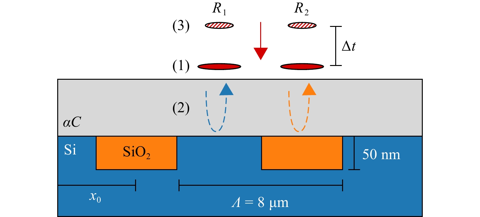
Fig. 1 Schematic of a SiO2 grating in Si, buried below amorphous carbon ($ \alpha {C} $), combined with a photoacoustic measurement. The grating is offset by $ x_0 $, and its depth and period ($ \varLambda $) are given for our sample. An optical pump pulse (1) generates an acoustic wave, which reflects from the bottom layer and travels back to the surface as an acoustic echo (2). After the pump pulse, at a time delay $ \Delta t $ that corresponds to the return of the echo, a probe pulse (3) arrives, and its reflection is accurately measured. The different bottom materials result in a local probe reflectivity of $ R_1 $ or $ R_2 $ over Si or SiO2, respectively.
-
We now analyze the details of retrieving $ x_0 $, and more importantly, how noise limits the reproducibility of determining $ x_0 $. Under the assumption that the focused probe laser spot is much smaller than the linewidth, the grating signal can be approximated by a square wave. The spatially resolved reflectivity at the optimal $ \Delta t $ is then given by
$$ R(x) = R_1 + \Delta R_{21} \cdot \sum\limits_{n = 0}^{\infty}A_n\cos\left(2n{\text{π}} (x - x_0) / \varLambda\right) $$ (1) where we have used the Fourier series of a square wave. Here, $ \Delta R_{21} = R_2 - R_1 $, $ A_0 = 1/2 $, and $ A_n = {{\sin c}}(n{\text{π}}/2) $. To determine the position of the grating, we only need to fit the fundamental ($ n = 1 $) cosine component, from which $ x_0 $ can readily be determined.
Any measurement will have some amount of noise, leading to inaccurate alignment. We now analyze a realistic experimental signal, which is based on the photocurrent of the detector that measures the reflected probe light. The (time-averaged) photocurrent is simply given by $ I(x) = I_0 \cdot R(x) / R_0 $, where $ I_0 $ is the photocurrent for the average unperturbed sample reflectivity $ R_0 $. Note that photoacoustic reflectivity changes are typically weak, so $ \Delta R_{21} << R_0 $. The $ n = 1 $ component of $ I(x) $ can be written as
$$ I'(x) = a\cos\left(2{\text{π}} x / \varLambda\right) + b\sin\left(2{\text{π}} x / \varLambda\right) $$ (2) with $ a = C\cos(2{\text{π}} x_0 / \varLambda) $ and $ b = C\sin(2{\text{π}} x_0 / \varLambda) $, using $ C = 2I_0\Delta R_{21}/({\text{π}} R_0) $. This form follows from trigonometric expansion of Eq. 1. The values $ a $ and $ b $ are the amplitudes of the Fourier components of $ I(x) $ with period $ \varLambda $, from which we can calculate
$$ x_0 = \frac{\varLambda}{2{\text{π}}}\tan^{-1}\left(\frac{b}{a}\right) $$ (3) In order to fundamentally understand how our method scales in terms of alignment accuracy, we assume that the only noise source is photocurrent shot noise. Since the average photocurrent is approximately $ I_0 $ in our weak-signal assumption, the variance on the Fourier series amplitudes of $ I(x) $ is given by32
$$ V_I \stackrel{\text{def}}{ = } {\rm{Var}}(a) = {\rm{Var}}(b) = 2 e I_0 \Delta f = 2 e I_0 / T $$ (4) Here, $ e $ is the electron charge and $ \Delta f $ the frequency spacing of the time-domain Fourier series, equal to $ 1 / T $ for a total measurement time $ T $. For a spatial scan speed $ v $ and scan length $ L $, the required time will be $ T = L/v $. Note that Eq. 4 only holds if the Fourier components are not attenuated by any filtering. Furthermore, in a real experiment the sampling Nyquist frequency needs to be sufficiently larger than the measurement bandwidth to avoid aliasing noise into lower-frequency bins. To first-order approximation and using the chain rule, from Eqs. 3, 4 we can derive
$$ \begin{split} {\rm{Var}}(x_0) \approx\;& \left|\frac{\partial x_0}{\partial a}\right|^2_{a,b} {\rm{Var}}(a) + \left|\frac{\partial x_0}{\partial b}\right|^2_{a,b} {\rm{Var}}(b) \\ =\;& \left(\frac{\varLambda}{2{\text{π}}}\right)^2\frac{V_I}{a^2 + b^2} = \left(\frac{\varLambda}{2}\right)^2\frac{e R_0^2 \Delta f}{2I_0\Delta R_{21}^2} \end{split} $$ (5) The alignment reproducibility or repro is then given by the standard deviation
$$ \sigma(x_0) = \frac{\varLambda}{2}\frac{R_0}{\Delta R_{21}} \sqrt{\frac{e}{2I_0T}} $$ (6) This scaling law enables prediction of which parameters to change and measure to improve and predict alignment accuracy. Note that when balanced detection is used (see Materials and methods), the reproducibility worsens by a factor $ \sqrt{2} $ because the current noise doubles.
Up to now, we have assumed that the measured signal is a square wave. However, if the probe spot size is not much smaller than the width of a grating line, the measurement will have a more rounded shape. Still, the signal can be represented as a Fourier series, and the $ n = 1 $ component can be used to find the grating position. For a square wave, this component has an amplitude $ A = 2\Delta R_{21}/{\text{π}} $ (see Eq. 1). For any other shape the noise analysis is still the same, with the reproducibility given by
$$ \sigma(x_0) = \frac{\varLambda}{{\text{π}}}\frac{R_0}{A} \sqrt{\frac{e}{2I_0T}} $$ (7) where A is the amplitude of the $ n = 1 $ Fourier component of the transient reflectivity signal.
-
We perform measurements on two samples with a layout as in Fig. 1, one with 600 nm and another with 1,300 nm thick amorphous carbon. These were fabricated by a semiconductor research and development organization (IMEC, Belgium). The samples were additionally annealed at 600 °C for 10 min. This increases film uniformity and etch selectivity of the amorphous carbon when used as a hard mask, at the cost of more opacity10. The sample with the 600 nm layer has a nominal reflectivity $ R_0 $ of 13.3%, with 14.2% for the 1,300 nm layer. Details of our method and setup for measuring transient reflectivity are provided in the Materials and methods section.
-
The transient reflectivity change after optical excitation of the 600 nm amorphous carbon layer is shown in Fig. 2a, for both Si and SiO2 bottom layers. The fast, near-instantaneous electronic response is large, but is not fully shown because we are interested in the ultrasonic signal. In general, the signals follow a slight rising trend due to thermal effects. Initially, the layer is hottest, and then slowly cools due to both transverse and longitudinal heat transport. In the first tens of picoseconds, the acoustic pulse can be seen leaving the surface of the opaque layer. Then, at around 240 ps, the acoustic pulse returns after reflecting from the bottom interface. The oscillatory shape is caused by Brillouin-like oscillations33, indicating that the optical penetration depth is at least on the order of the probe wavelength in the layer. The amplitude of the echo in the reflectivity signal depends on the buried material. On top of bare Si, the amplitude is larger than over the region with grown SiO2.
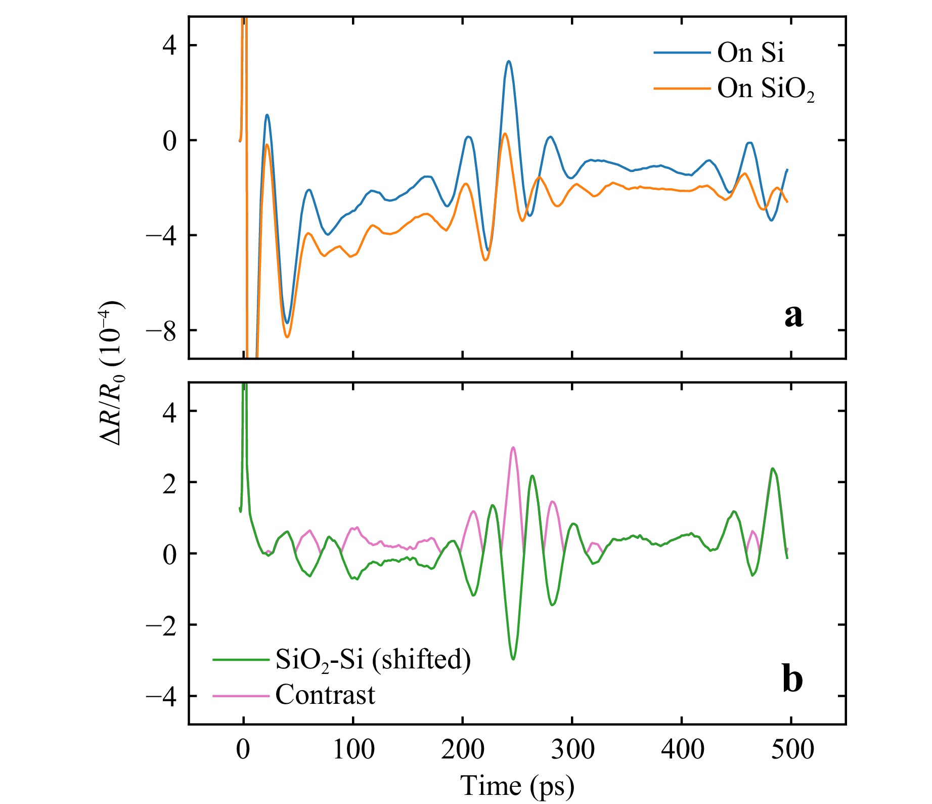
Fig. 2 a Transient reflectivity signal after pump excitation of the 600 nm amorphous carbon layer, on an area with either Si or SiO2 below. The first acoustic echo returns after approximately 240 ps, and has a larger amplitude on top of Si. The offset difference likely results from optical effects due to partial transparency of the amorphous carbon. b The difference between the SiO2 and Si signal, shifted such that the mean is around zero. Where this difference is negative, we plot the absolute value to indicate the contrast. Maximum contrast occurs at 245 ps.
In addition to the difference in echo amplitude, the traces also have different offsets, even at times when the echo is not visible. We attribute this effect to the layer not being fully opaque, making the reflection from the back interface depend on the buried material. The different offsets can then be caused by two mechanisms. Firstly, the amount of absorbed pump pulse energy can be different for the Si or SiO2 bottom layer. However, the echo amplitude on Si is larger, whereas its thermal background is smaller (closer to 0), which cannot be explained by absorption effects alone. More significantly, the layer forms a kind of (single-reflection) Fabry-Pérot etalon, where the back interface has a material-dependent reflectivity. The thermally induced refractive index change modifies the optical path length of the layer, phase shifting the back-reflected probe light with respect to the front-reflected probe light. The intensity of the reflected light then changes due to interference, with the strength depending on the reflection coefficient of the back interface34.
The difference between the two signals, with the offset removed, is plotted in Fig. 2b. We also attribute the initial oscillating difference to the optical effect mentioned above, as the acoustic pulse should be identical at this point. However, since the acoustic reflection depends on the interface, the maximum contrast at around 245 ps is mostly caused by acoustics. So, the buried layer can already be identified by the transient reflectivity amplitude at 245 ps, with Si giving an approximately 3 × 10⁻⁴ higher relative reflectivity change.
-
For a thicker amorphous carbon layer at equal penetration depth, the optical interference effect should diminish. This is already the case for a 1,300 nm thick layer, as shown in Fig. 3a. The initial acoustic pulse looks similar to the one in Fig. 2a, but there is no offset anymore at later times. At around 460 ps, the echo returns. However, assuming that the speed of sound is the same in both layers, the echo should instead be expected at around 520 ps. Therefore, we conclude that either the layer thicknesses deviate slightly from their design, or the speed of sound is different, possibly due to different annealing outcomes.
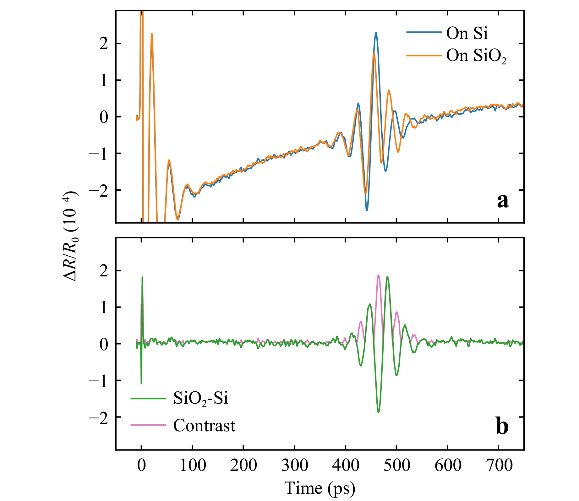
Fig. 3 Similar to Fig. 2, but now for the thicker 1,300 nm amorphous carbon layer. a Here, the round trip time is around 460 ps. For this layer, there is no offset between the signals, because the layer is now fully opaque. b The difference between the SiO2 and Si signal, with maximum contrast at 465 ps.
We can again easily distinguish the Si bottom layer from SiO2. Even though the acoustic pulse almost traveled twice as far compared to the 600 nm layer, the difference in relative reflectivity change is still around 1.8 × 10⁻⁴.
-
As explained in the introduction, if the underlying Si-SiO2 layer is structured, spatially scanning the pump and probe together across the sample at an optimal pump-probe delay should reveal the structure by a spatially varying transient reflectivity signal. One of the buried Si-SiO2 structures is a large grating with 8 µm pitch, with alternating 4 µm Si and SiO2 buried lines. See Fig. 1 for a schematic overview of the sample. Fig. 4 shows spatial scans over this grating at different fixed delay times for the 1,300 nm sample. The grating lines are well-resolved because of the small probe spot size (1.0 µm). In the pump-probe delay direction (vertical), the curves look like the difference curve from Fig. 3b, divided by two. Similarly, the peak-to-peak amplitude in the position direction (horizontal) is equal to the difference curve. Therefore, the maximum visibility also occurs at 465 ps here. Because the transient reflectivity change at this delay is lower for SiO2 than for Si and the spatial oscillation is initially negative, the scan started on a SiO2 line. To calibrate the optimal pump-probe time delay, it is sufficient to perform a measurement as in Fig. 3 once. The exact delay time here needs to be accurate to within 5 ps, as the grating can quickly become invisible if the delay time is wrong. For example, compare the spatial scan at 465 ps, which has good contrast, to the scan at 475 ps, in which the grating is invisible.
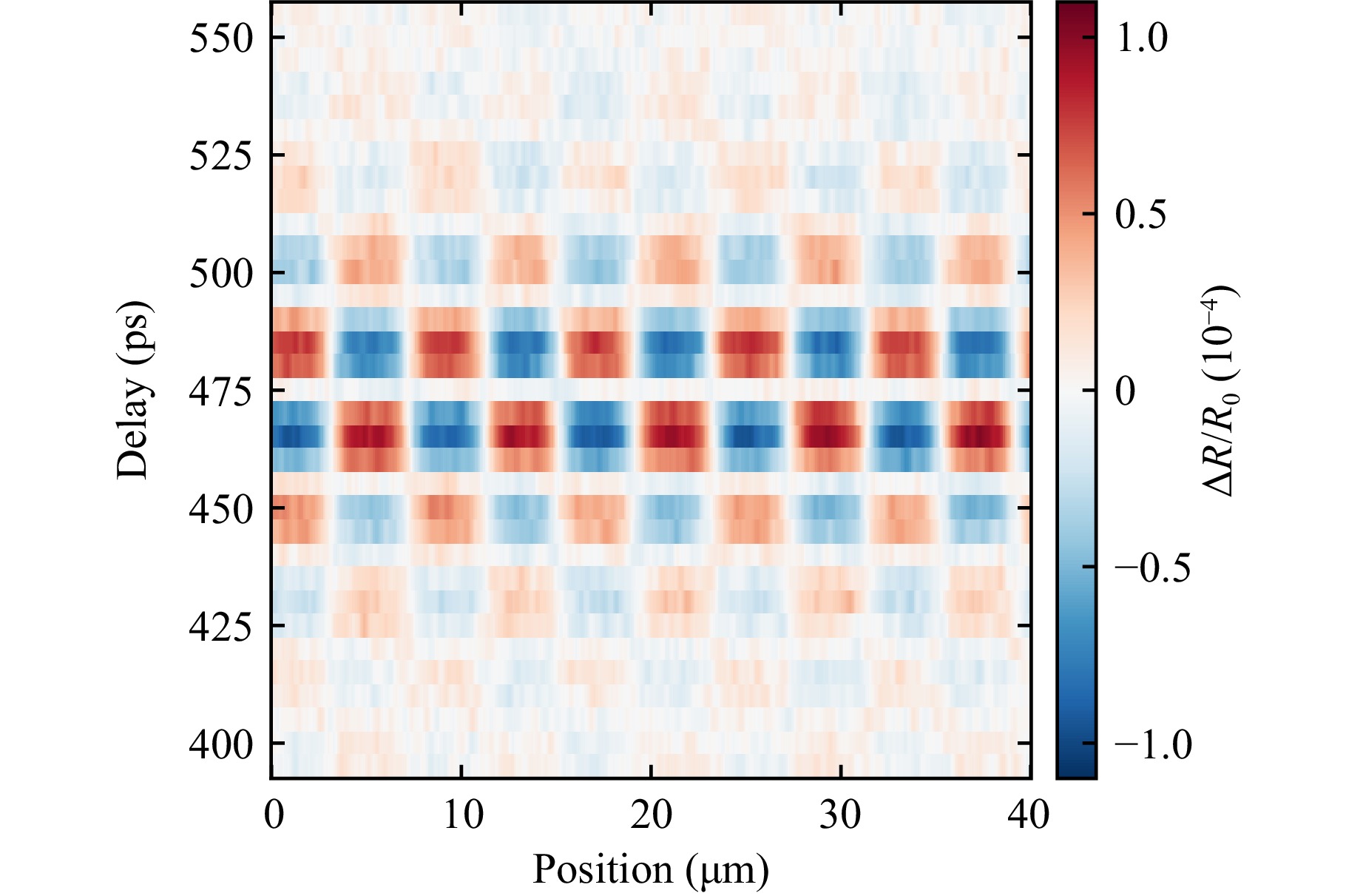
Fig. 4 Spatial scans over an 8 µm grating underneath the 1,300 nm amorphous carbon layer, at varying pump-probe delay times with steps of 5 ps. Each row is offset by its mean. At zero crossing times of the trace in Fig. 3b, the grating is nearly invisible.
-
Spatial scans at the optimal pump-probe delay of 465 ps enable nanometer-level alignment of the buried grating. Typically, the global, approximate grating position with respect to the movement stage is found using the finite size of the grating. Next, accurate alignment is achieved by scanning over the grating and determining the offset position of it using a cosine fit. Our grating has a size of 2 mm, so with a small scan length the global position cannot be found. However, we can determine the local offset position over a length of 100 µm from a single scan. For example, the scan in Fig. 5 has an offset position of 1.24 µm for the first SiO2 line. Note that the actual signal is not exactly a cosine wave, but a rounded square wave. This is also visible in the colored scans in Fig. 4. However, the cosine wave fit accuracy does not suffer from this, as it essentially only looks at the position of the first harmonic of the square wave and ignores higher orders (see Introduction).
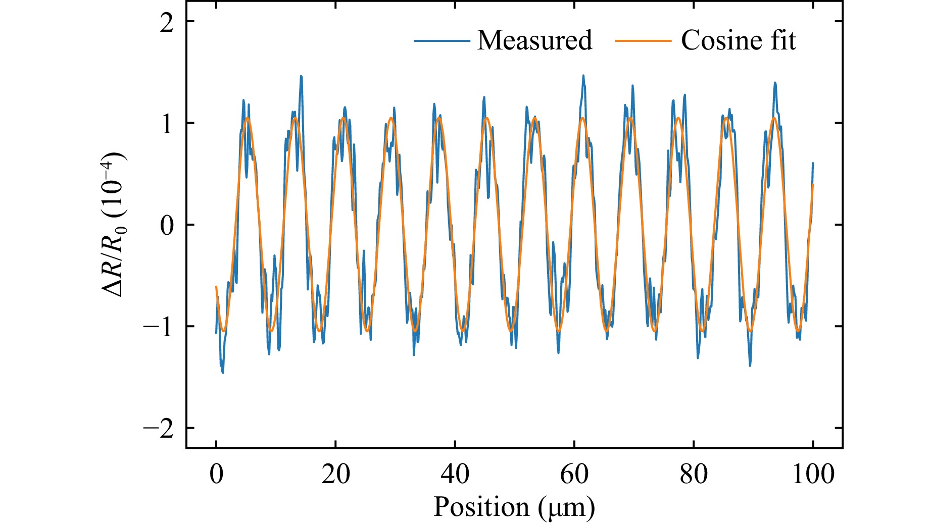
Fig. 5 Transient reflectivity signal during a spatial scan over the grating at a fixed pump-probe delay of 465 ps for the 1,300 nm amorphous carbon layer, offset by its mean. The total integration time for the measurement is 0.8 s. From the cosine fit and given that $ \Delta R_{21} \lt 0 $ at this delay, we find that the offset of the first SiO2 line is 1.24 µm.
The accuracy or reproducibility of the determined position is critically important for semiconductor wafer alignment. Our scanning stage is however not stable enough to repeat many scans in order to determine the standard deviation of the cosine fit offset. Regardless, we can still assess the achievable repro from the measured signals. To this end, we fit a cosine to the left 50 µm half of the data and another to the right half of the data. Then, the reproducibility over many scans can be determined from the standard deviation of the difference in the cosine offsets for both halves. Note that each fit has $ \sqrt{2} $ worse standard deviation because it only uses half of the data, and that taking the difference between the two fit offsets results in another factor $ \sqrt{2} $ overestimation. The resulting reproducibility is therefore reduced by a factor of 2 to correct for this. We have verified the correctness of this analysis method by retrieving a known reproducibility from a Monte Carlo simulation of generated data.
At a total integration time of 0.4 s, the reproducibility of alignment already reaches 20 nm. This standard deviation is based on 512 scans over the grating. By averaging groups of these 512 scans together, we can emulate longer integration times. The reproducibility for different total integration times is plotted in Fig. 6. As predicted by Eq. 6, the reproducibility scales inversely proportional to the square root of integration time, with 14.7 nm at 1 s.
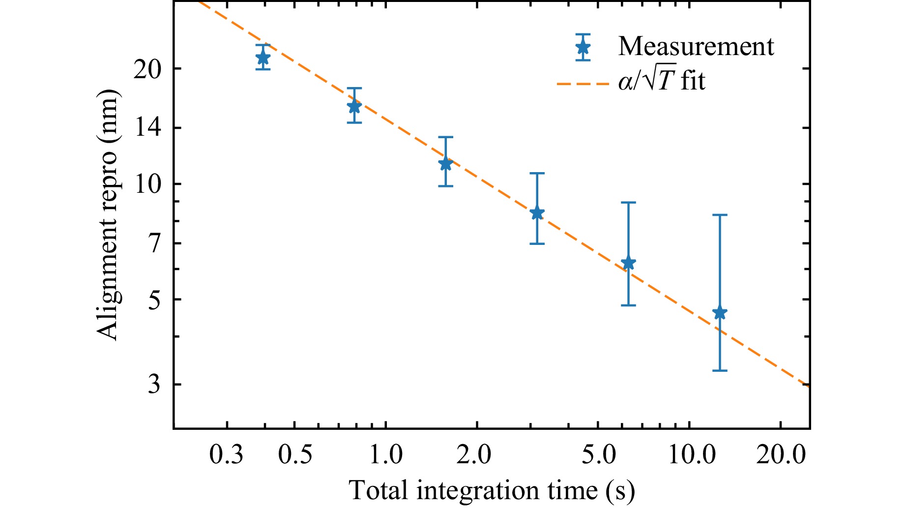
Fig. 6 Alignment reproducibility of the buried grating for the 1,300 nm amorphous carbon layer, as a function of total integration time. The error bars indicate the 90% confidence interval based on the chi-squared distribution of variance35. As expected, the scaling follows an $ \alpha / \sqrt{T} $ trend, with $ \alpha $ approximately $ 14.7\;\text{nm}\;\sqrt{ \text{s}} $.
-
The measurements on the 1,300 nm layer of the $ \varLambda = $8 µm grating have a maximum $ \Delta R_{21}/R_0 $ of approximately 1.8 × 10⁻⁴ (see Fig. 3). Furthermore, the average photocurrent here is around 6.8 µA. Using Eq. 6, with the additional factor $ \sqrt{2} $ because of balanced detection (see Materials and methods), we get an expected reproducibility of 3.4 nm at 1 s. Similarly, considering that the signal is not an exact square wave, we get a value of 3.8 nm using Eq. 7 and a fit amplitude of approximately 1.0 × 10⁻⁴ (see Fig. 5). Our experimental alignment accuracy is around four times worse than these predictions. We have verified that the amplitude noise floor of our measurement is nearly shot-noise limited, with only 23% additional RMS (root-mean-square) noise. Furthermore, we have verified Eqs. 6, 7 with Monte Carlo simulations as well. We therefore suspect that the stick-slip piezo movement stage we use to scan the sample has residual jitter that limits the achievable fit accuracy. Even though we try to reduce the effect of the stage by comparing the left and right halves of the data, jitter on smaller spatial scales will remain. However, this positional noise should still reduce by $ 1/\sqrt{T} $ with averaging, which is what Fig. 6 shows. Another possibility for the worse-than-theory result is that there is high-frequency beam movement of the probe and/or pump beam. Beam drift is especially problematic for the probe beam, as it directly couples into phase noise of the grating. The pump spot is almost four times bigger, so pump drift is less problematic. Furthermore, pump beam fluctuations only couple into amplitude noise as the pump-probe overlap changes, but as stated we do not observe significantly more amplitude noise than shot noise. In a different measurement with almost four times more fluence, we do observe significantly more noise than shot noise. We attribute this to laser-induced damage to the amorphous carbon layer, which reduces reflectivity36. The increased spatial reflectivity gradient will lead to more noise if the probe beam fluctuates.
-
Decreasing the gap between experiment and theory would be possible with a smoother and more accurate stage. Pump and probe beam stabilization will also decrease phase and amplitude fluctuations of the grating signal. Fundamental improvements can only be made by optimizing the parameters in the reproducibility equation (Eq. 6). Reducing the period is a simple way to linearly improve alignment accuracy, but the line widths cannot be made narrower than the probe spot size. As mentioned before, we can also pump with more fluence, at the cost of increased damage. In our measurement with four times more fluence, the relative reflectivity change also increases by a factor four approximately. However, this causes damage in the form of a permanent few percent reflectivity drop in the pumped area. The pump fluence will thus have to be optimized while taken acceptable damage levels into account. Obviously, the probe fluence can also be increased, but similar considerations have to be made.
Another improvement would be to increase pump and probe power at constant fluence. This increases alignment accuracy by the square root of optical power, because the relative contribution of shot noise decreases. A way to achieve higher optical powers can be to use elliptical spots instead of round spots, aligned with the long axis in the direction of the grating lines. Furthermore, the laser spots can also be made in the form of a grating themselves, with a period similar to that of the alignment grating, by combining beams at an angle17, 37.
-
There are more materials in use in semiconductor fabrication steps that are opaque, such as ruthenium. Ruthenium can be used for very thin conductive lines, as the resistivity of ruthenium lines can be better than copper at critical dimensions below about 10 nm38. Here, higher aspect ratios using thicker layers of ruthenium reduce resistance as well. Another possible use of ruthenium is as hard mask material39. Similar to amorphous carbon, thicker ruthenium (order 100 nm) layers can improve etch selectivity. At such thicknesses, ruthenium is essentially completely opaque. However, ruthenium supports very high-frequency laser-induced ultrasonics due to strong electron-phonon coupling, has a high optical damage threshold, and acoustic waves are visible to near-infrared laser light as well40. These properties potentially make picosecond ultrasonics a relevant method for alignment through ruthenium as well.
In a realistic application scenario, the exact stack composition may be complex and not known a priori. That means that the optimum time delay for alignment measurements should be determined experimentally by performing a time-delay scan at a marker location. Such a scan provides information similar to Figs. 2, 3 from which an optimum time delay for further measurements can be derived. This measurement takes on the order of seconds, and only needs to be done once before processing a full batch of wafers with a given design.
-
In conclusion, we demonstrate that picosecond ultrasonics provides a viable route towards optical metrology on semiconductor samples that contain optically opaque materials. The achieved repro scaling for an 8 µm pitch grating underneath a 1,300 nm thick amorphous carbon layer is $ 14.7 \;\text{nm}\;\sqrt{\text{s}}$. While further improvements are needed to reach the throughput requirements of semiconductor alignment metrology, several improvements have been identified that can bring the method to the required performance level. The acoustic-strain-induced reflectivity change is the main parameter that determines the signal strength. This is a material property that can have widely different values for different materials and probe laser wavelengths41. In practice, this means that selecting an optimal probe wavelength for a given material should be part of the measurement strategy.
The use of ultrafast acoustic waves for metrology and imaging has further potential, as the wavelength and spatial extent of the acoustic pulses are significantly shorter than optical wavelengths. Picosecond ultrasonics has already been used to measure thin-film properties13, 17, 34. An extension to other forms of semiconductor metrology such as profilometry can therefore be envisaged.
-
The pump-probe setup is based on a variant of asynchronous optical sampling (ASOPS)42 and is illustrated in Fig. 7. A pump (1,030 nm, 180 fs, Menlo Systems) and a probe (780 nm, 80 fs, Menlo Systems) laser are co-linearly focused onto the sample through a 0.45 NA objective (Olympus LUCPLFLN20X). The full width at half maximum spot sizes are 3.8 µm and 1.0 µm for pump and probe, respectively. For all measurements, the pump energy is 2.6 nJ (114 J/m2), and the probe energy 0.028 nJ (18 J/m2). The lasers are electronically synchronized to tune the time delay between them. In conventional ASOPS, the entire pump pulse time interval is measured, which reduces efficiency if the time window of interest is shorter. Instead, we rapidly modulate the time delay over only the window of interest, greatly reducing the total integration time at equal noise levels. For more information on the setup and a detailed analysis of the benefits of modulated ASOPS (MASOPS)43. The reflected probe light is measured using a balanced detector (Koheron PD10B with Thorlabs FDS02 photodiodes), with the reference input split off from the probe laser before it hits the sample. In our experiments, we pulse pick the pump to 1 MHz and the probe to 2 MHz, and do lock-in detection (Zurich Instruments UHFLI) of the probe light at 1 MHz. Pulse picking increases the signal-to-noise ratio on our samples, as it allows for higher fluence and thus signal, while not increasing damage as much36. Due to technical limitations we actually measure 8 million probe pulses per second, but the resulting shot noise doubling is corrected for in the analysis.
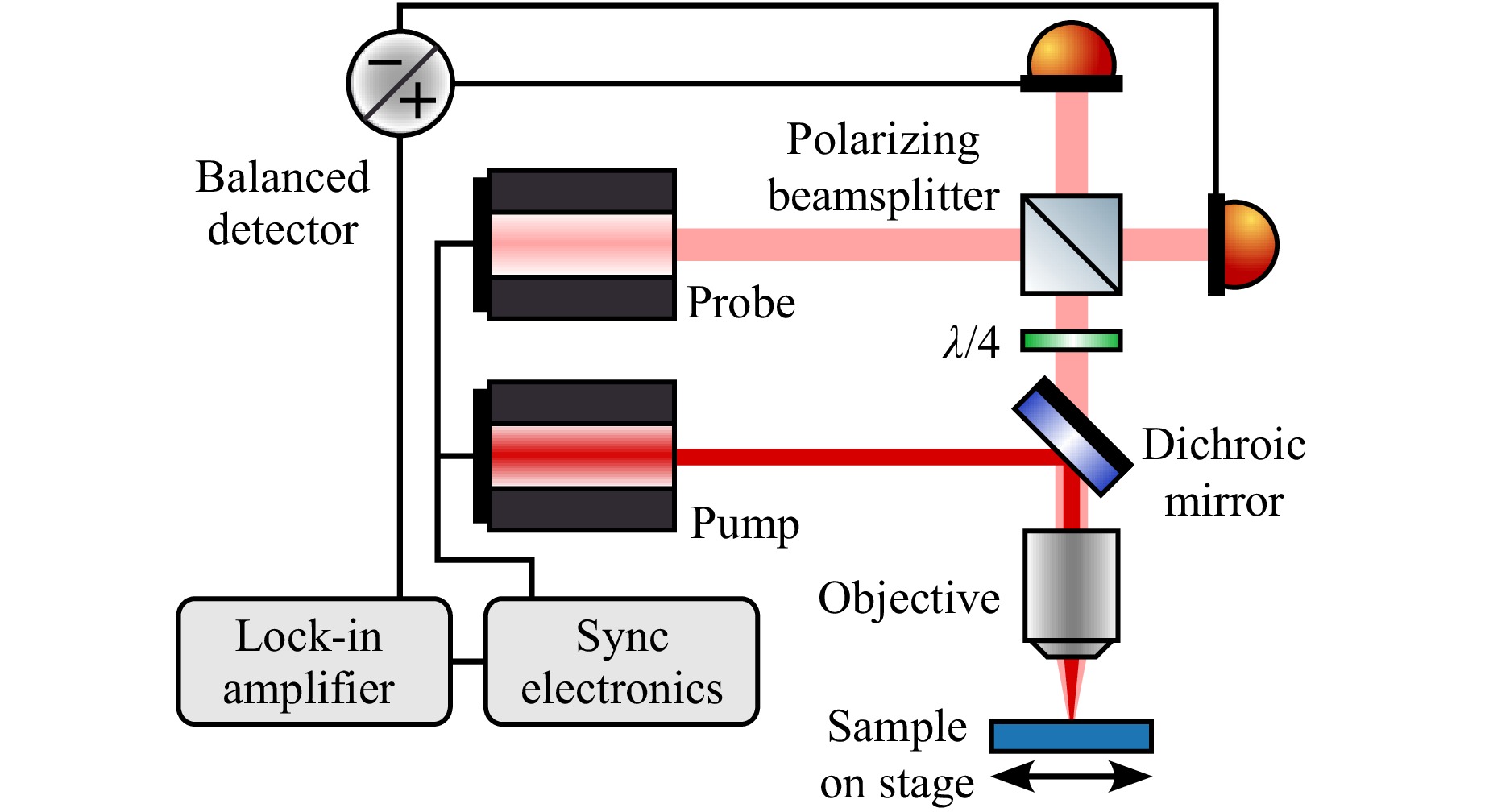
Fig. 7 Schematic of the pump-probe setup. An objective co-linearly focuses the pump and probe laser beams onto the sample, which is mounted on a translation stage. The reflected probe light is analyzed with a balanced detector and a lock-in amplifier. Synchronization electronics control the pump-probe delay time. For more details, see the text and references36,43.
-
Instead of scanning the pump-probe delay in time, we can also keep the delay constant at a fixed delay time. By then moving the sample stage, we can measure the spatially varying pump-induced probe signal. Similar to scanning in time, fast scanning in space is important to avoid flicker noise contributions that significantly increase noise for long integration times. With our stage, we scan a distance of 120 µm across the buried grating back and forth at 2 Hz, with an average scan speed of 480 µm/s. The position curve has the same shape as the time curve that we use in MASOPS43, with the middle 90% linearly scanned. We therefore analyze only a 100 µm portion in the middle of the trace. Due to acquisition limitations we can only extract the average scan of at least two traces, meaning the minimum exposure time is approximately 0.4 s. The stage is a stick-slip piezo stage (SmarAct SLC1730 with MCS2 controller), which has nanometer-level accuracy, but not perfectly smooth continuous motion due to the stick-slip action.
-
The authors thank Paul Planken for insightful discussions, and Marco Seijnen from the AMOLF/ARCNL software engineering department for support in experiment automation. We acknowledge the support from the European Research Council (ERC-CoG 864016, project 3D-VIEW), and the Dutch Research Council NWO (TTW-HTSM 17960, project Orpheus). This work was conducted at the Advanced Research Center for Nanolithography, a public-private partnership between the University of Amsterdam (UvA), Vrije Universiteit Amsterdam (VU), Rijksuniversiteit Groningen (RUG), the Dutch Research Council (NWO), and the semiconductor equipment manufacturer ASML.
Nanometer-level metrology through opaque layers using laser-induced picosecond ultrasonics
- Light: Advanced Manufacturing , (2026)
- Received: 19 November 2025
- Revised: 18 May 2026
- Accepted: 18 May 2026 Published online: 22 July 2026
doi: https://doi.org/10.37188/lam.2026.083
Abstract: Manufacturing integrated circuits (ICs) using photolithography is the key technology enabling modern electronic devices. As advanced ICs are fabricated in multiple lithography steps, accurate metrology is crucial. For wafer alignment, optical methods are essential as they enable fast and non-invasive measurements. However, the use of optically opaque materials complicates optical metrology on markers in deeper layers. Here we present an optical metrology approach capable of nanometer-level alignment metrology through optically opaque layers. We use ultrashort laser pulses to generate high-frequency ultrasound at picosecond timescales, with which buried metrology markers can be probed. By detecting the ultrasound reflections with a second, time-delayed laser pulse, position information is obtained in an all-optical way. We demonstrate our approach on an alignment grating covered by a 1.3 μm thick layer of amorphous carbon, achieving 15 nm positioning reproducibility in 1 s measurement time, with significant potential for further scaling. This measurement concept will help advance semiconductor manufacturing, by enabling optical wafer metrology on future devices featuring layers of metals and other opaque materials.
Research Summary
Optical metrology: precision measurements through opaque media with light-induced sound
Matthias Velsink and co-workers from ARCNL, Delft University of Technology and ASML demonstrate a measurement concept that enables optical metrology through thick layers of opaque materials. In the fabrication of integrated circuits using lithography, accurate positioning is crucial for reliably manufacturing nanoscale devices. Optical measurement methods are essential to ensure that positioning can be done fast and without damage, but many materials encountered in semiconductor manufacturing are not transparent to light. The authors exploit the phenomenon that light can generate ultrasound in opaque media, and use that ultrasound to probe metrology markers hidden below the opaque layers. They detect the returning ultrasound using light and retrieve highly accurate positioning information in a short measurement time. This work may open new routes for optical metrology in semiconductor applications involving opaque media.
Rights and permissions
Open Access This article is licensed under a Creative Commons Attribution 4.0 International License, which permits use, sharing, adaptation, distribution and reproduction in any medium or format, as long as you give appropriate credit to the original author(s) and the source, provide a link to the Creative Commons license, and indicate if changes were made. The images or other third party material in this article are included in the article′s Creative Commons license, unless indicated otherwise in a credit line to the material. If material is not included in the article′s Creative Commons license and your intended use is not permitted by statutory regulation or exceeds the permitted use, you will need to obtain permission directly from the copyright holder. To view a copy of this license, visit http://creativecommons.org/licenses/by/4.0/.

 DownLoad: