





-
Micro-light-emitting diodes (Micro-LEDs) are rapidly emerging as a transformative technology for high-resolution displays1,2, offering exceptional brightness, fast response times, high contrast ratios, and ultra-low power consumption3,4. Their compact pixel architecture and excellent optical properties make them particularly attractive for next-generation display applications, including augmented and virtual reality (AR/VR)5,6, smart wearables7,8, and advanced mobile displays9. Compared to conventional liquid crystal displays (LCDs)10 and organic light-emitting diode (OLED) technologies11, micro-LEDs deliver superior pixel-level control, enhanced durability, and a wider colour gamut, making them promising candidates for future full-colour microdisplay platforms9,12. However, the construction of a complete RGB micro-LED display presents significant challenges. Traditional approaches, such as mass transfer, suffer from limitations in alignment precision, processing time, and high fabrication costs13. Efficiency mismatches also block scaling, and red micro-LED components tend to show a lower external quantum efficiency (EQE), which makes the system-level balance harder14. A more practical route uses quantum dot colour-conversion (QDCC) layers on top of the blue micro-LEDs. This setup supports tunable red, green, and blue emission, which simplifies high-resolution display architectures15,16. QDCC-layer-based systems face several major issues. The main one is precise micropatterning with a resolution beyond the retinal limit17.
Current QDCC layer-patterning methods include inkjet printing18, photolithography19,20, and transfer printing21; each has its own limitations. Inkjet printing often produces uneven films; however, it also leads to QD aggregation, droplet size variation, and ink spreading, which reduce pixel accuracy and weaken edge definition. Nozzle clogging and critical ink formulations also lower process reliability. Photolithography supports high-resolution patterning but uses multistep UV exposure workflows. They also have limited three-dimensional structuring ability, and solvent-based etching can harm the optical integrity of quantum dots (QDs). As the pixel size decreases, maintaining a precise mask alignment becomes increasingly challenging. As demonstrated in prior work, the patterned perovskite quantum dots (PQDs) with pixel sizes down to 2 µm can be produced using photolithography22. Despite these results, complex workflows and high material loss restrict the suitability of scalable micro-LED display manufacturing23. In addition, transfer printing avoids solvent exposure and supports broad material compatibility; however, high-resolution patterning remains difficult. The stamp deformation, placement errors, and mechanical stress increase sharply below 5 µm and reduce pattern accuracy and yield. In addition, its contact-based mechanism risks damaging delicate QDs during transfer, and the repetitive, time-intensive stamping process limits its scalability13,14,24.
To overcome these disadvantages, laser-drilling-based micropore filling22 has gained much research attention as a simple and highly efficient approach for fabricating high-resolution QDCC layers25. Unlike traditional photolithographic techniques, laser drilling is a maskless process that eliminates the need for harmful chemicals, thereby reducing contamination risks and preserving the optical quality of QDs. This maskless, lithography-free, and noncontact method provides micron-scale precision26, with high automation making it well suited for scalable integration in next-generation full-colour micro-LED displays25. As demonstrated in previous works, fibre-laser drilling has been used to create micropores down to 35 µm, enabling efficient QD filling without solvents, photoresists, or etching agents that degrade QD quality. However, fibre lasers have limitations in achieving higher drilling precision because of the unavoidable generation of a heat-affected zone (HAZ), particularly at the micron and submicron scales25.
To address these limitations, ultrafast laser sources, particularly femtosecond (fs) lasers, have been increasingly adopted for microscale and nanoscale material processing27,28. Fs lasers operate with pulse durations in the order of 10−15 s29. These timescales are far shorter than the electron-phonon coupling and thermal diffusion times of most solid materials30. As a result, the laser energy enters the electronic system before lattice heating begins. This interaction regime suppresses thermal diffusion into the surrounding material, thereby minimising HAZ formation and preserving the structural integrity at small feature sizes. Owing to these characteristics, fs lasers enable cleaner and more precise material removal than conventional thermally driven laser systems, particularly for feature sizes below 5 µm31. Their high peak intensities promote nonlinear absorption mechanisms, such as multiphoton ionisation, enabling efficient ablation of polymeric and transparent32 materials with minimal collateral damage33. Previous reports have demonstrated that a 1,030 nm fs laser drill of tungsten is achieved with sizes as small as 17 µm34. Beyond clean ablation, fs lasers offer versatile beam control, including beam shaping, wavelength tunability, and pulse tailoring, which enables flexible micro- and nanomanufacturing across a wide range of materials. Compatibility with single- and multi-pulse operations, combined with selective material removal due to distinct ablation thresholds, further enhances the processing precision and material integrity. Collectively, these attributes make fs lasers particularly suitable for advanced micro-LED fabrication and QD integration processes25.
One major challenge for QDCC layers is their high sensitivity to moisture and air, which quickly degrades their optical performance35. To reduce this degradation, (SU-8)36, an epoxy-based negative photoresist37, serves as a protective matrix with high mechanical rigidity, chemical resistance, optical transparency, and low cost. Researchers have deposited SU-8 by spin coating and patterned it using standard ultraviolet (UV) photolithography. This workflow supported the direct integration of silicon (Si) and glass substrates38. SU-8 also supports next-generation display concepts because SU-8 works with flexible substrates. This property supports rollable, conformal screen designs, and SU-8 also fits fs laser microdrilling workflows. This matching supports the fabrication of high-resolution pixel arrays with controlled feature placement and stable film protection. Earlier findings indicate that the fs laser Bessel-beam is able to create taper-free microholes in poly methyl methacrylate (PMMA), achieving diameters of 1.5−2.4 µm31. These findings highlight the potential of ultrashort-pulse lasers for producing the sub-5 µm pixel structures required for advanced micro-LED displays. Although fs-laser processing has been established as a highly effective tool for high-precision fabrication, the generation of high-quality micropores remains a technical challenge. This requires precise control of the laser-material interaction, accurate beam focusing, beam alignment, and suppression of undesirable effects such as debris formation, HAZ, and potential substrate damage. These factors influence the uniformity, size, and circularity of the resulting QD pixels.
To address the above limitations of conventional QDCC layer patterning and pixel scaling for micro-LED displays, this study presents a maskless fabrication strategy that combines fs laser drilling with micropore templating in an SU-8 polymer. SU-8 was deposited on glass substrates by spin coating to form a uniform thin film, which was subsequently patterned by fs laser drilling using both Gaussian and Bessel-beam profiles to evaluate the influence of beam shaping on microhole formation and process reliability. Fig. 1 presents a schematic of the complete optical system used for laser drilling, including the optical beam path and laser source. A photograph of the laser setup is shown in Fig. S1. These laser-drilled microholes later functioned as micropore moulds for QD filling to form patterned QDCC layers. Within this framework, Bessel-beam irradiation enables the formation of uniform, circular, and taper-free microholes with diameters as small as 100 nm, producing clean, well-defined edges without an observable HAZ, which is essential for reliable QD filling and pixel uniformity. By tuning focal depth and pulse energy, controlled microhole arrays are fabricated over a large area of 17 mm × 15 mm with a drilling rate of at least 100 holes s−1; this rate is not fundamentally limited by the laser system and can be further improved through parallel or multi-beam approaches. These nanoscale microholes function as pixel-level containers for QDs, enabling the formation of single- and dual-colour CdSe QD patterns and QDCC layers with high uniformity across different pixel sizes. Finally, a fully transparent encapsulation layer is applied to seal the QD-filled structures and protect them from moisture and environmental degradation. Overall, this approach provides a scalable, solvent- and lithography-free route for defining nanoscale pixels, thereby supporting the manufacture of high-resolution QDCC layers required for micro-LED displays in AR/VR applications.
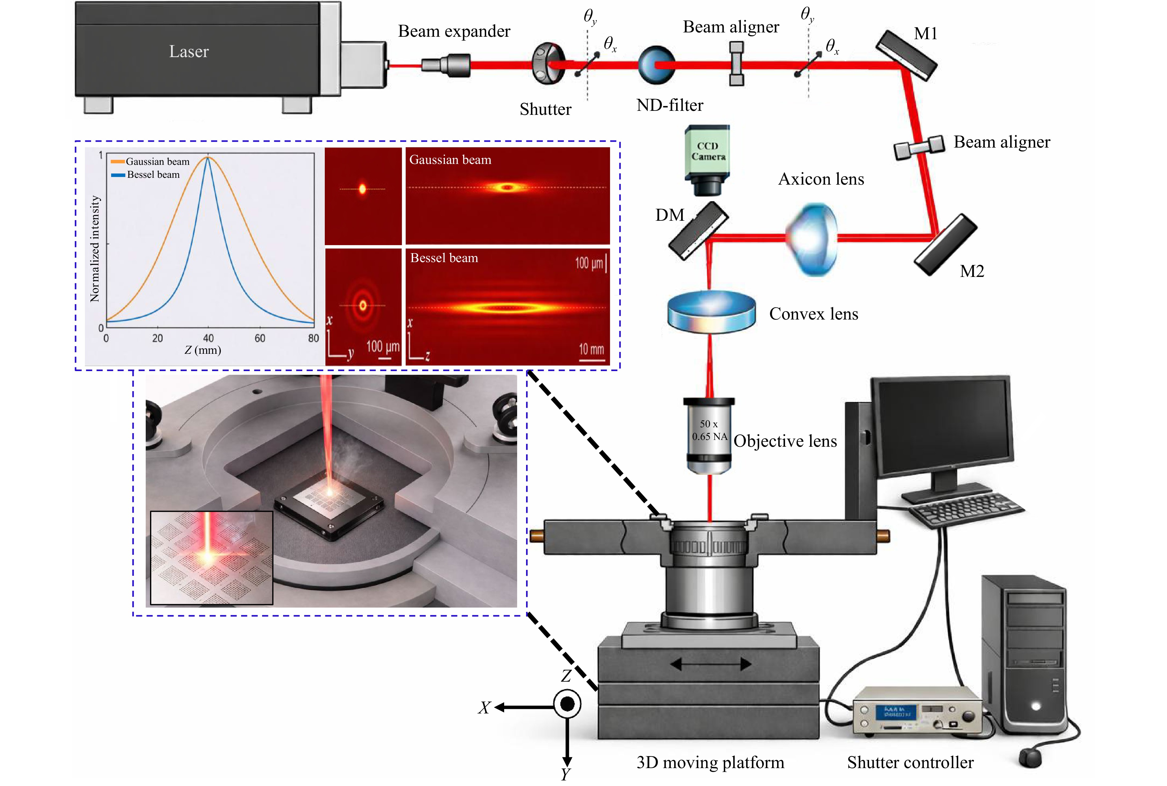
Fig. 1 Experimental setup for fs laser drilling, including beam-shaping optics for Gaussian and Bessel beams, a 50× objective lens, a charge-coupled device (CCD) monitoring camera, and a motorized translation stage. The Gaussian beam with a confined focal intensity and the Bessel beam with an extended axial core and concentric ring structure are used for drilling.
-
This study experimentally investigated fs-laser-induced microscale hole fabrication in an SU-8 photoresist for micro-LED QDCC layers, with particular attention to the concentric-ring effect under different beam configurations. Achieving large-area, high-quality, circular, homogeneous microholes is essential for this application. Both Gaussian and Bessel beams were examined, and the effects of repetition rate, pulse count, and pulse energy on hole quality were systematically evaluated (see the supplementary, for the experimental setup and detailed procedures).
Fs laser drilling with a Gaussian beam was investigated to fabricate high-quality taper-free microholes. Fig. 2a-c present scanning electron microscopy (SEM) images of transparent SU-8 microholes fabricated at a pulse energy of 5 µJ and a repetition rate of 100 Hz, with pulse counts ranging from 1 to 12. Fig. 2a shows that a single-pulse irradiation produces a small inlet diameter of 1 µm but fails to fully ablate the SU-8 layer, leaving residual material inside the drilled region and causing noticeable edge deformation. These results indicate that a single pulse does not provide sufficient energy for complete material removal under Gaussian beam irradiation; therefore, the number of pulses was increased to five to enhance material removal. The results show that an increase in the pulse number leads to a slight improvement in material removal. At the 5th pulse, Fig. 2b shows a deeper hole and a wider inlet diameter of 1.2 µm. At this stage, SU-8 removal was concentrated at the centre, whereas the residual material remained near the edges. This pattern reflects the Gaussian beam intensity distribution with a bell-shaped profile across the beam cross-section, as the Gaussian beam remains confined over a limited propagation range39. A glass surface affected by the laser is observed in the middle of the hole. This result shows that increasing the number of pulses enhances the material removal and produces deeper micropores; however, excessive pulses can affect the glass substrate. This behaviour arises because, during multi-pulse drilling, the initial pulses remove the upper portion of the SU-8 layer, exposing the substrate so that subsequent pulses directly interact with the glass. At the 12th pulse, Fig. 2c shows further SU-8 removal and a pore diameter of approximately 1.3 µm. Meanwhile, microcracks form, the edges deform, the HAZ grows, and the glass substrate shows clear damage. These features indicate that thermal overexposure is driven by excessive pulse accumulation. Overall, these results demonstrate a clear trade-off in Gaussian beam drilling. Multi-pulse irradiation improves the penetration depth, but it also increases the hole size, degrades the surface quality, and restricts the suitability for fabricating the small and homogeneous micropores required for high-performance micro-LED QDCC layers.
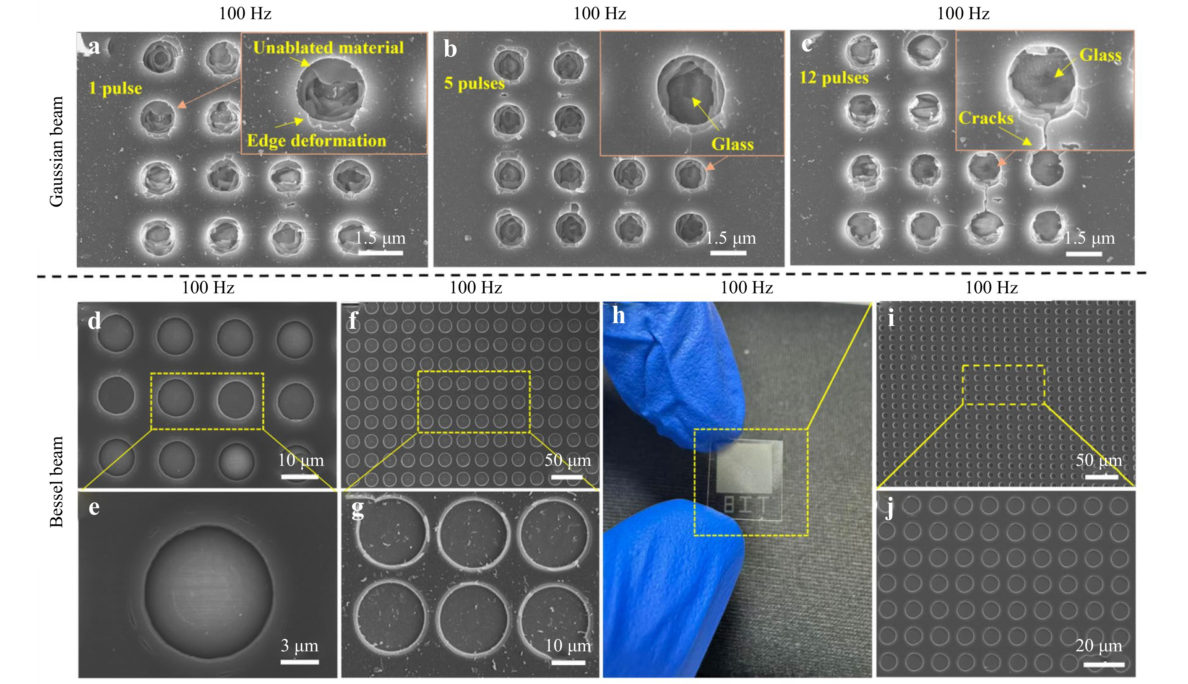
Fig. 2 SEM characterisation of fs-laser-drilled microholes in SU-8 photoresist. a-c Gaussian-beam-drilled microholes at E = 5 µJ and R = 100 Hz with pulse counts of 1, 5, and 12. d-e Single-pulse Bessel-beam drilling at 27 µJ, 100 Hz and f-g at 34 µJ, 100 Hz. h-j A large array fabricated with 25 µJ at a repetition rate of 100 Hz.
To evaluate the performance differences between Gaussian and Bessel beam drilling, an axicon and a convex lens were added (see the supplementary). The incident Gaussian beam was directly focused through the objective lens (OL) while maintaining the same laser configuration and focal position used in the Bessel beam setup. High-quality taper-free microholes were fabricated using single-pulse fs Bessel beams with a concentric ring effect, in contrast to Gaussian beam irradiation, as shown in Fig. 2d-j. As illustrated in Fig. 2d, a single Bessel-beam pulse (27 µJ, 100 Hz) produces uniform microholes with a diameter of 11 µm, which is further confirmed by the magnified view in Fig. 2e. When the pulse energy is increased to 34 µJ, and the repetition rate is 100 Hz, microholes with a clear circular entrance and a larger mean diameter of approximately 20 µm are achieved, as shown in Fig. 2f, 2g. These results confirmed that the pore diameter was primarily governed by the applied pulse energy, whereas the spacing between adjacent microholes depended on the scanning speed and repetition rate. The Bessel beam behaves as a nondiffracting and self-healing40, with a narrow central core surrounded by concentric rings. In the Bessel beam, the central core has the highest intensity, whereas the outer rings have lower intensities and are gradually activated as the pulse energy increases, leading to more pronounced peripheral ablation and disk-shaped edge features at higher energies. Fig. 1 shows the Gaussian and Bessel beam profiles. Furthermore, the results showed that single-pulse drilling efficiently removed the SU-8 layer while avoiding damage to the underlying glass substrate. However, increasing the number of pulses led to substrate damage, as shown in Fig. S2, demonstrating that single-pulse fs Bessel beam drilling provides improved machining quality compared with multiple-pulse percussion drilling.
After a comprehensive understanding of the factors affecting the microhole morphology, a “flying punch” approach was employed using single-pulse femtosecond Bessel-beam irradiation to generate highly uniform microhole arrays, as shown in Fig. 2h-j. This technique demonstrates excellent machining efficiency and reproducibility, yielding low-aspect-ratio pores with a consistent geometry over large areas. A periodic array was fabricated in SU-8 by applying a pulse energy of 25 µJ at a repetition rate of 100 Hz, with each microhole formed by a single laser shot with a diameter of 8 µm. The scan speed was maintained at 1.3 mm·s−1, which determined the centre-to-centre pore spacing of 13 µm according to the relation d = v/f, where d is the hole centre-to-centre spacing, v is the translation speed, and f is the laser repetition rate. The SU-8 surface was positioned at the midpoint of the beam focal depth to optimise the ablation efficiency. Under these conditions, uniformly distributed microholes were produced over an area of 17 mm × 15 mm, corresponding to approximately 1.5 million pores (Fig. 2h), with a fabrication rate of 100 pores·s−1. This fabrication rate was used to demonstrate the feasibility of the experimental configuration used in this study, and was not limited to this processing speed. In practice, the same laser system can operate at higher repetition rates41, which can significantly increase the number of pulses per second. Furthermore, the fabrication throughput can be further improved by implementing parallel multi-beam processing, where a single laser beam is divided into multiple beams to enable the simultaneous drilling of multiple micropores42. Such strategies are particularly suitable for the ablation of polymers, such as SU-8, because the required single-pulse energy is minimal (in the range of tens of microjoules). This process was performed using a computer-controlled six-axis translation stage to ensure precise positioning and high pattern consistency. As shown in Fig. 2h-j, the resulting arrays exhibit excellent uniformity, with magnified views confirming a clean pore morphology and consistent profiles.
Figs. 3a-p shows that, by modulating the pulse energy while maintaining a constant repetition rate and optical alignment, a series of micro- and submicron-scale holes with controlled diameters were fabricated using single-pulse femtosecond Bessel-beam irradiation. At the pulse energies from 46 µJ to 14 µJ (see the supplementary), well-defined pores with mean diameters of approximately 37 µm and 1.8 µm were obtained, as shown in Fig. 3a-h. It is not feasible for the centre-to-centre spacing to remain fixed across all the pulse energies. At a fixed spacing, increasing the pulse energy increased the pore diameter and reduced the interwall thickness, which may degrade the SU-8 framework. As shown in Fig. 3b, a minimum interwall thickness of approximately 8 µm is required to maintain structural integrity under the investigated conditions. Further reductions in pulse energy to 10 µJ and 4 µJ, submicron features with diameters of 1 µm and 100 nm were successfully generated, as shown in Fig. 3i-p, with magnified views of the smallest pores presented in Fig. 3p. Across all the investigated energy levels, the fabricated micro- and nano-holes exhibited good circularity and high uniformity, indicating the high precision of the Bessel beam ablation process. During fabrication, some debris was observed around the holes; however, loosely attached debris could be removed through simple, gentle nitrogen blowing or gas-flow cleaning without affecting the micropore geometry43. These results demonstrate that a wide range of aperture sizes can be achieved by precisely controlling the pulse energy and beam parameters, which is particularly advantageous for the fabrication of micro-LED QDCC layers. However, consistent feature size and pixel-level accuracy are crucial for display performance.
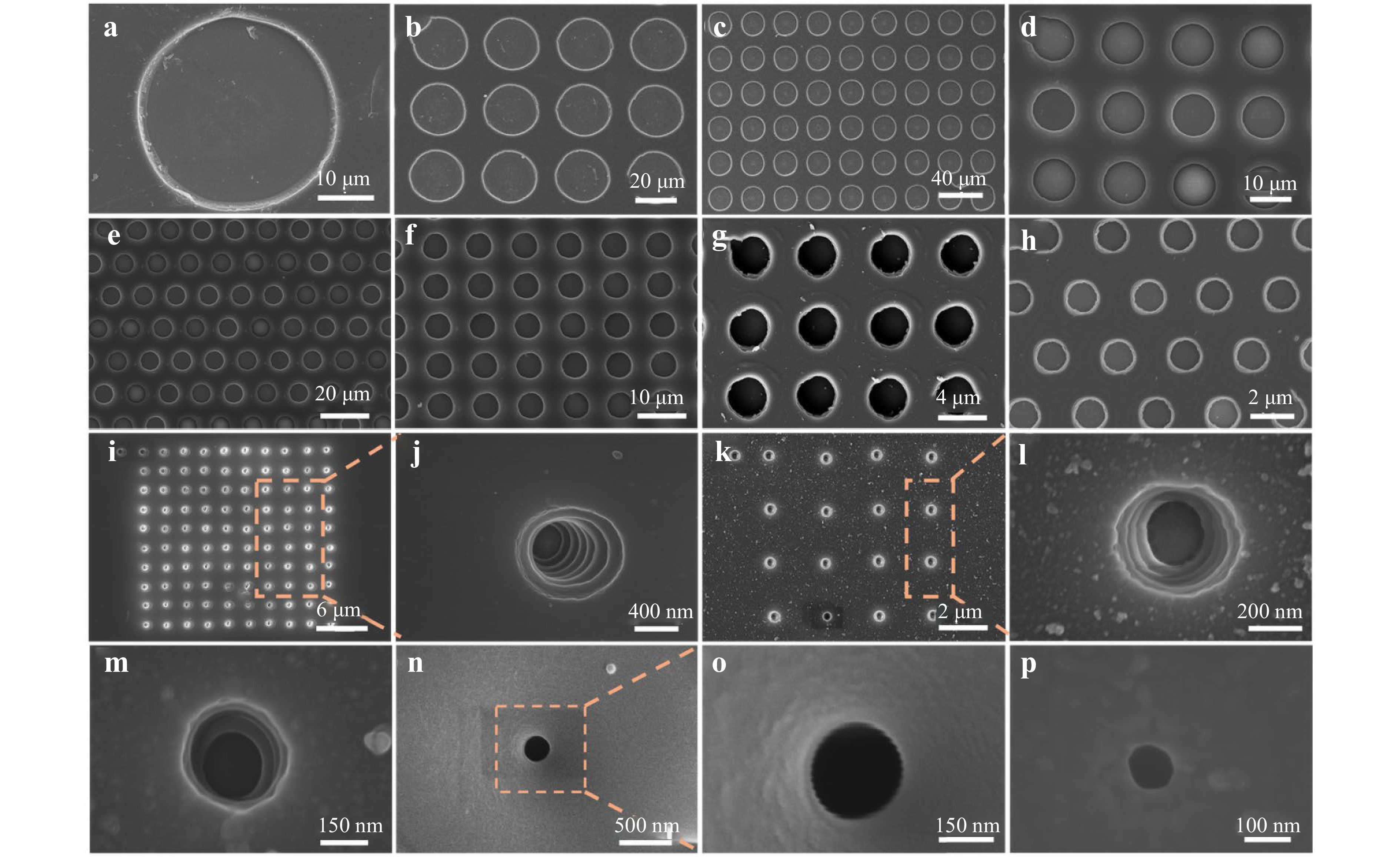
Fig. 3 SEM images of fs-laser-drilled SU-8 microholes with diameters ranging from 37 µm down to 100 nm. a-g Larger pores (37 µm to 3.5 µm) exhibit smooth boundaries and well-defined circular profiles. h-j Small pores (1.8 µm to 1 µm). Furthermore, panels k-p show the nanoscale holes (500 nm to 100 nm).
-
The fabrication of single-colour CdSe QDCC layers involves five sequential steps: SU-8 spin coating (see the supplementary), laser drilling, QD gel filling, UV curing, and surface polishing, as illustrated in Fig. 4a. First, a micropore mould was fabricated on an SU-8-coated substrate using fs laser drilling; the SEM images are shown in Fig. 3a-p. Next, green or red UV-curable CdSe QDs were dispensed onto the mould using a micropipette. To ensure uniform infiltration, the QDs were spread across the surface using a squeegee; this step pushed the CdSe QD material into the micropores (see the supplementary). At the micro- and nanoscales, liquid infiltration into small cavities is governed by interfacial effects such as wetting behaviour and capillary forces at the pore openings44. The forward and backward spreading of the QD solution across the surface during the filling process helped to distribute the QD gel more uniformly and facilitated its penetration into the micropores. The viscosity of the QD solution also influences the filling behaviour, because lower-viscosity solutions can flow more readily into small cavities. After filling, the sample was exposed to UV light for approximately two minutes, and the surface was polished to remove unwanted material. This method produced a clean, fluorescent QDCC layer structure, as shown in Fig. 4b, c (see Fig. S4a-i for the single-colour QDCC layers). Using this approach, we patterned large-area QD arrays to produce green pixels with 3.5 µm diameters (Fig. 5a) and red pixels with 7 µm diameters (Fig. 5b). This method can be used to control the micropore diameter, depth, and spacing by tuning the laser pulse energy, scanning speed, and SU-8 mould thickness.
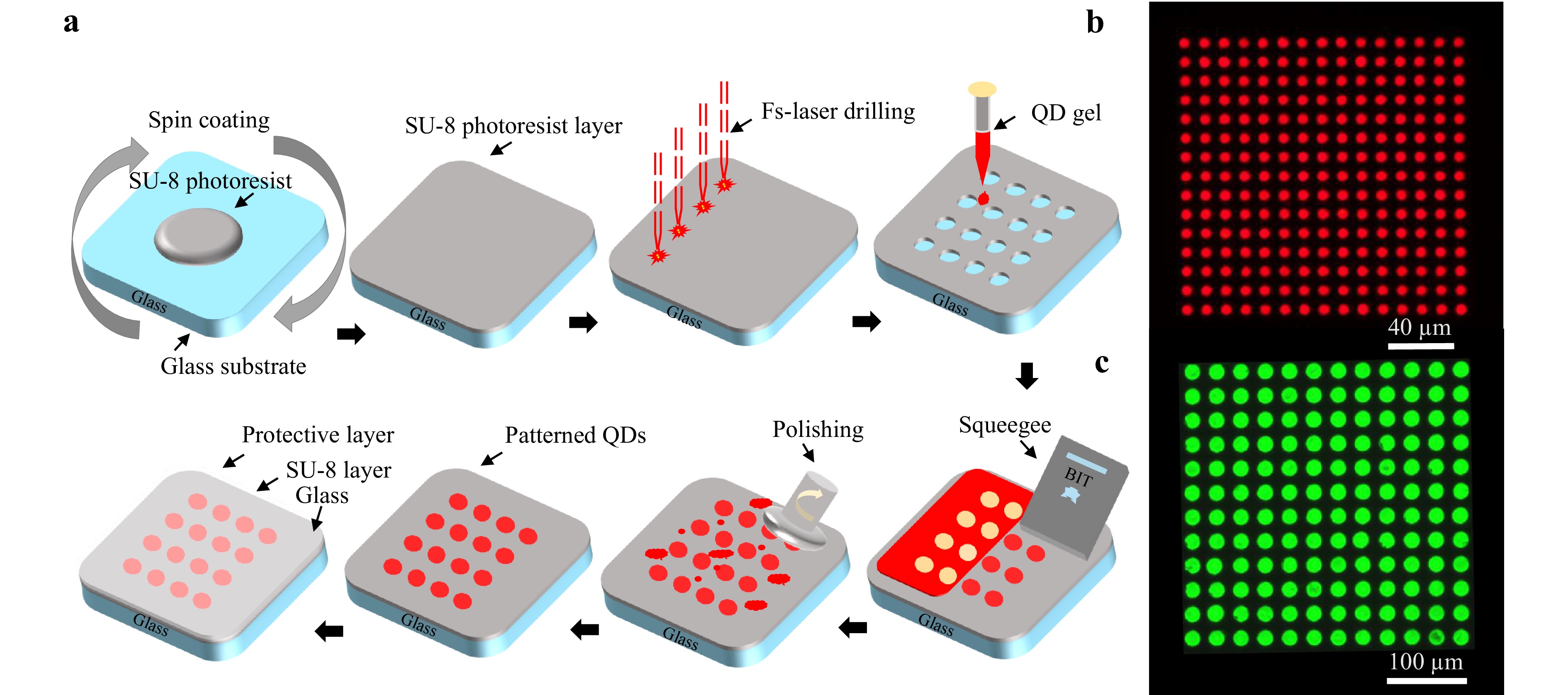
Fig. 4 a Schematic illustration of the fabrication process for single-colour QDCC layers using fs drilling and a micropore-filling technique. b, c Fluorescence images of representative monochrome CdSe QD arrays with micropore diameters of 6 µm and 22 µm, respectively.
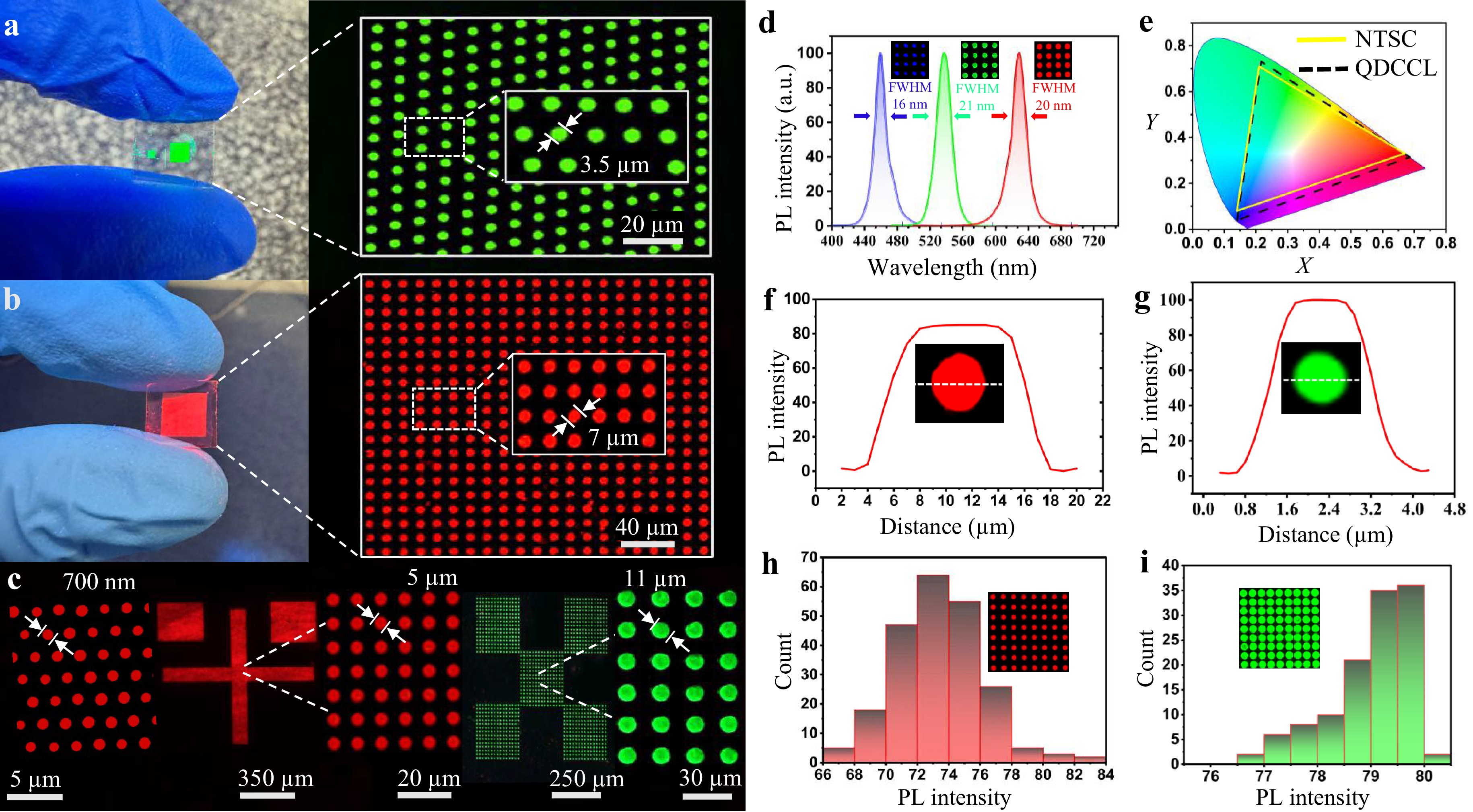
Fig. 5 Photographs and fluorescence images of a green (3.5 µm) and b red (7 µm) large-area CdSe QD arrays fabricated by laser-drilled micropore filling. c Fluorescence images of high-resolution QD patterns featuring pixel diameters of 700 nm, 5 µm, and 11 µm. d Photoluminescence emission spectra of the green and red CdSe QD arrays, exhibiting narrow full widths at half maximum (FWHMs) of 21 nm and 20 nm, respectively. e Corresponding colour-gamut mapping showing 111% NTSC coverage. f, g Line-scan PL intensity profiles across individual red and green pixels, demonstrating uniform emission. h, i PL-intensity histograms obtained from PL mapping, showing that 93% of red-pixel intensities fall within 68−78 and 93% of green-pixel intensities lie within 78−80, confirming excellent pixel-to-pixel uniformity across the arrays.
As a proof-of-concept, green and red QD arrays with pixel diameters of 11 µm and 5 µm, as well as red QD arrays with pixel diameters of 700 nm, were fabricated and verified by fluorescence imaging (Fig. 5c). Although fs laser drilling achieves nano-holes with diameters down to 100 nm, it highlights the capability of the laser processing approach. However, reliable QD filling at this scale faces challenges, including fluid behaviour, infiltration efficiency, and packing of QD materials within highly confined geometries. In this study, hole diameters of up to 700 nm were selected to achieve uniform QD filling and consistent optical output; however, further advances in QD material design and filling strategies are required to enable precise nanoscale QD pixels. The laser-drilled micropore filling method provides guidance towards the future development of clean and homogenous holes below 500 nm. Further, Fig. S4a-i shows the increase in the diameter of the fabricated micropores. The geometry of the laser-drilled micropores is also a key factor in obtaining homogeneous QD emissions because inappropriate ablation or SU-8 residues may decrease the excitation efficiency and cause uneven pixel brightness. When the laser conditions were optimised, clean circular pores containing CdSe QDs were obtained (Fig. S5). When the parameters were not ideal, the pores were distorted in shape and the polymer remained inside the micropore mould. The cross-sectional images in Fig. S6 confirm that the QDs remained confined within the SU-8 cavities after UV curing. Furthermore, the SEM images recorded before and after the QD filling (Fig. S7a-d; see the supplementary) demonstrate complete and uniform micropore filling.
In addition, the photoluminescence (PL) characteristics of the patterned CdSe QD arrays were evaluated using fluorescence microscopy. Under excitation from a 460 nm blue micro-LED, the green and red CdSe QD layers showed emission peaks at 537 and 628 nm, respectively. Their spectral widths remained narrow, at 21 and 20 nm, respectively (Fig. 5d). The small spectral overlap supports high colour purity in the fabricated CC layers, and colour gamut mapping shows 111% National Television System Committee (NTSC) coverage (Fig. 5e), demonstrating its suitability for wide-gamut microdisplay applications. The pixel-level brightness uniformity was checked using line-scan PL analysis. The 3.5 µm green pixels and 7 µm red pixels keep stable PL intensity across their diameters (Fig. 5f, g), and local PL mapping also shows the same pattern. Further in the 10 µm red array, 93% of PL values fall between 68 and 78, and in the 20 µm green array, 93% of intensities fall between 78 and 80 (Fig. 5h, i). These results highlight the consistent emissions across the entire array. However, the optical crosstalk, blue light leakage, and conversion efficiency are also important for micro-LED QDCC layers. In this study, transparent SU-8 was used to demonstrate the feasibility of a micropore fabrication process based on fs laser drilling. The nanoscale drilling results and QD pixels suggest that this method is not limited to transparent SU-8 and can be applied to black SU-8 and other polymers, which may help to improve the control of optical crosstalk. The optical conversion efficiency and blue light leakage in practical devices can be improved by filling QDs with deeper holes in practical devices45. To quantify brightness uniformity in accordance with the Chinese electronic industry standard for LED displays, the luminous uniformity IRJ was calculated from 30 randomly selected pixels in each array using the following equation:
$$ {I}_{RJ}=1-\frac{{|I_i-\overline{I}|}_{max}}{\overline{I}}\times 100\% $$ Here $ I_i $ is the fluorescence intensity of an individual pixel, and $ \overline{I} $ is the arithmetic mean of the intensities of the 30 selected pixels (see the supplementary). With this method, the red pixel array shows 90% uniformity and the green array reaches 97%; both values exceed the minimum national requirement. Laser-drilled micropore-filled CdSe QD structures deliver high colour purity, stable emission, and strong pixel-to-pixel brightness uniformity, making them a strong fit for micro-LED colour conversion applications.
-
As shown in Fig. 6a, dual-colour QDCC layers are produced by repeating the laser-drilled micropore-filling process using green and red QDs, as described in the (see the supplementary). During fabrication, repeated squeegee coating promoted complete QD infiltration into the micropores, whereas a subsequent polishing step removed the excess QD material without damaging the filled micropores. The patterned structure is then encapsulated by a thin layer of transparent photoresist, which enhances environmental stability and provides long-term optical performance (see Fig. S3a-c for the complete full-colour QDCC layers). Three micropore array designs were produced, as shown in Fig. S8a-f. Fig. S8a and S8b show the single-colour micropore patterns before and after QD filling, respectively, whereas Fig. S8c and S8d show micropore arrays containing red and green CdSe QDs, respectively. To complete the RGB architecture, a QD-free micropore array was introduced during the final fabrication step, as shown in Fig. S8e and S8f, where the red and green QD-filled micropores were combined with a third QD-free micropore to allow blue light emission from the underlying blue micro-LED. The resulting structures formed well-aligned high-resolution arrays. Fig. 6b, c are representative fluorescence images of the dual-colour patterns, with an average pixel size of 11 µm and the dimensions of the array 13 × 10 pixels. These structural findings highlight the importance of an accurate micropore geometry and layer design to ensure high-performance QDCC layers.
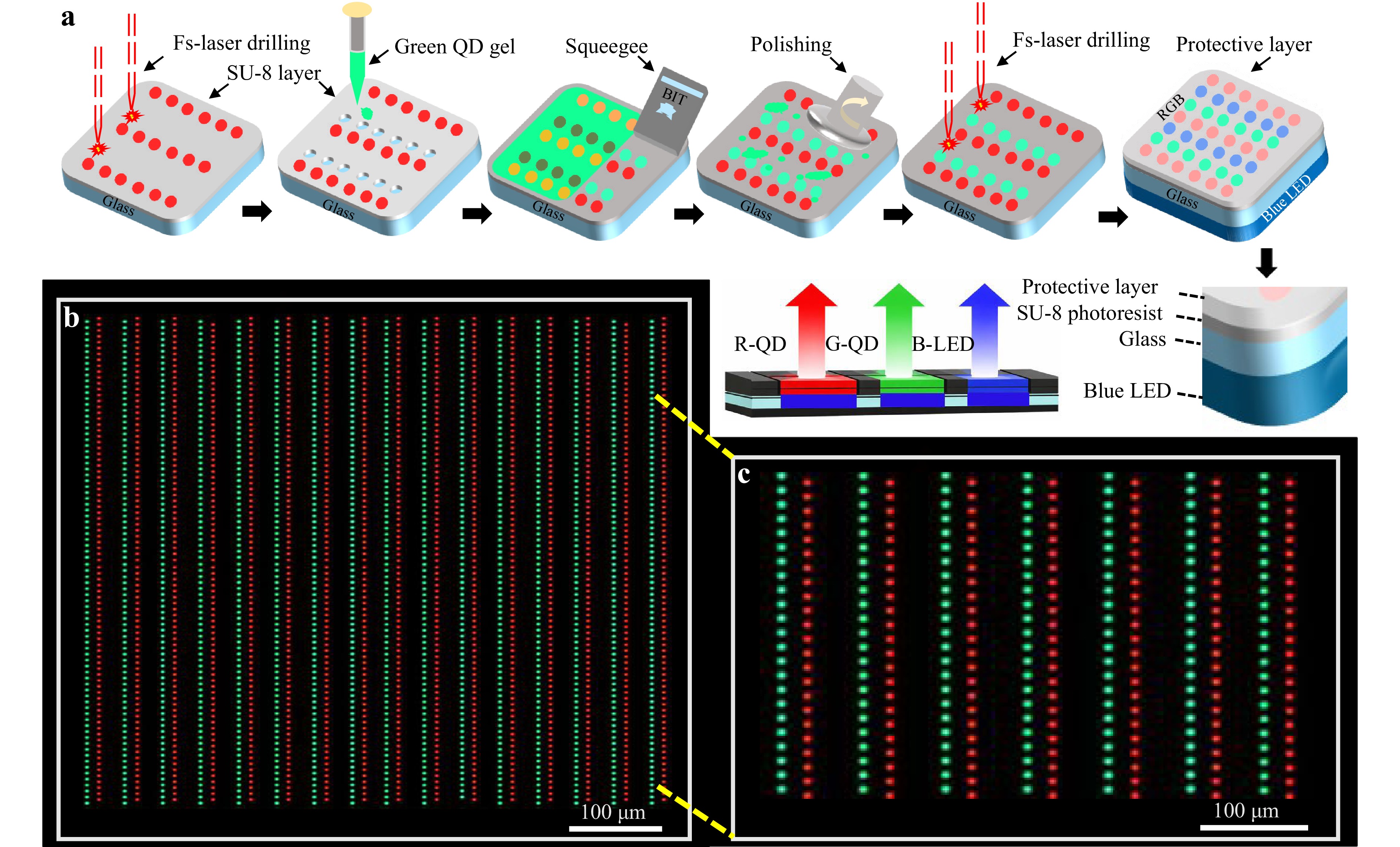
Fig. 6 a Schematic illustration of the sequential fs laser-drilling and micropore-filling process used to fabricate dual-colour CdSe QDCC layers. b, c Fluorescence images of representative dual-colour QD arrays, showing uniform pixel formation, clear colour separation, and accurate spatial alignment over large areas.
The critical dimensions and thicknesses of the layers are also important factors in the fabrication of QDCC layer next-generation displays. High spatial resolution requires an ever-smaller pixel, whereas a wide colour gamut requires blue photon leakage into the red and green subpixels to be suppressed46. In our work, the fabrication of micropore moulds with diameters as low as 100 nm, together with the achieved 111% NTSC colour gamut coverage, demonstrates that the proposed approach can meet these requirements and enable high-quality QDCC layers for future display technologies. In addition, this method offers several practical advantages, including the rapid fabrication of large-area, uniformly patterned QD arrays, a solvent-free removal process that avoids material compatibility issues commonly encountered in conventional lithography, and partial recovery and reuse of QD gels during squeegee coating, thereby reducing material waste. These scalable processing strategies, such as high-speed scanning and multibeam approaches, together with the maskless and solvent-free nature of the programmable fabrication process, help reduce the overall operational cost of fs-laser processing and enhance its practicality for large-scale micro-LED fabrication.
Overall, the laser drilling and micropore-filling strategy presented here provides an effective route towards QDCC layers with enhanced spatial resolution and offers a viable pathway for high-performance full-colour displays integrated with blue micro-LEDs. Beyond smart QDCC layer integration, with the micropore filling method, the same fs fabrication strategy can also be implemented for direct laser interaction with QD layers47 or other functional polymer thin films for pixelated electroluminescent devices, which typically consist of multilayer architectures. The ability of fs laser processing combined with appropriate optical system engineering, such as beam shaping, beam splitting, and single-pulse irradiation, to achieve high-fidelity patterning, cavities, 3D geometries, and layer-by-layer material removal with minimal material damage makes the method broadly applicable to other technologies. These include image sensors, biomedical devices48 involving localised functional or bioactive material integration, pixelated electroluminescent devices, and optical memory or data storage systems49, in which well-defined micro/nanoscale cavities are essential for information encoding and retention50. Thus, the laser-defined micropore-filling platform provides a scalable, material-agnostic, and high-precision manufacturing method for next-generation optoelectronic, sensing, biomedical, and photonic systems.
-
In this study, we present a fs-laser-driven microhole drilling and QD filling strategy for fabricating high-resolution CdSe QDCC layers. This maskless and solvent-free approach enables precise pixel definition in SU-8 polymers using Bessel-beam ablation, achieving tunable pixel diameters from several micrometres to 100 nm. The SU-8 micropore mould serves both as a structural scaffold and a protective barrier for the embedded QDs and is further encapsulated by a transparent photoresist layer to ensure long-term environmental stability. Optical characterisation confirmed narrow QD emission spectra, with full widths at half maximum (FWHMs) of 21 nm for green emissions and 20 nm for red emissions, as well as a wide colour-gamut coverage of 111% NTSC. Pixel-level uniformity was demonstrated through line-scan photoluminescence (PL) profiles and statistical PL mapping, with 93% of the red pixel intensities distributed within the range of 68−78 and 93% of the green pixel intensities within 78−80. The corresponding luminous uniformities reached 90% for the red pixels and 97% for the green pixels, exceeding the established electronic display standards. This method further supports sequential laser drilling and QD filling to realise dual-colour arrays with clean boundaries and high pattern fidelity over large areas. Collectively, these results establish a scalable and highly reproducible platform for next-generation micro-LED displays, particularly for AR/VR systems and compact high-density colour-conversion architectures.
-
This work was supported by the National Key R&D Program of China (2022YFB4601300), the National Science Foundation of China (NSFC) General Program (Grant No. 52475425) and the Basic Sciences Centre Program (Extreme Light Field Manufacturing, Grant No. 52488301). We thank the Biological and Medical Engineering Core Facilities of the Beijing Institute of Technology and the Experimental Centre of Advanced Materials at the Beijing Institute of Technology for their support in characterisation. We also acknowledge Prof. Haizheng Zhong for useful discussions.
Spatially shaped femtosecond-laser-assisted 100 nm ultrafine patterning of quantum dots for high-resolution micro-LED displays
- Light: Advanced Manufacturing , Article number: 89 (2026)
- Received: 07 February 2026
- Revised: 30 May 2026
- Accepted: 01 June 2026 Published online: 17 August 2026
doi: https://doi.org/10.37188/lam.2026.089
Abstract: High-resolution pixelated patterning of quantum dot colour-conversion (QDCC) layers is of significant importance for advancing display technologies. However, a significant challenge lies in the fabrication of high-resolution pixel templates with submicron precision and geometric uniformity. In this study, a high-precision and scalable femtosecond (fs) laser drilling method is used to fabricate microhole arrays in SU-8 polymers. The results show that, compared with Gaussian beams, Bessel-beam irradiation enables the formation of taper-free microholes with smooth sidewalls and diameters as small as 100 nm, while preventing damage to the underlying glass substrate. The fabricated microholes are used as a micropore mould to fabricate monochrome and dual-colour QDCC layers by precisely filling them with CdSe QDs. These layers exhibit narrow-band fluorescence with full widths at half maximum (FWHMs) of 21 nm (green) and 20 nm (red), high colour purity, and a wide colour gamut reaching 111% of the National Television System Committee (NTSC) standard. Pixel-level photoluminescence (PL) mapping confirms homogeneous emission, with 93% of both red- and green-pixel intensities falling within narrow ranges and luminous uniformities of 90% and 97%, respectively. This maskless and solvent-free process offers a promising platform for high-resolution QDCC layers in augmented reality/virtual reality (AR/VR) systems and next-generation micro-light-emitting diode (micro-LED) displays.
Research Summary
Spatially Shaped Femtosecond-Laser-Assisted 100 nm Ultrafine Patterning of Quantum Dots for High-Resolution Micro-LED Displays
Micro-light-emitting diode (micro-LEDs) displays require precise and scalable Quantum dots colour-conversion (QDCC) layers. QDs are attractive colour-conversion materials because of their narrow emission bandwidth, high colour purity, and solution processability. However, forming small, uniform, and well-aligned QD pixels remains challenging. Conventional methods such as inkjet printing, photolithography, and transfer printing often suffer from limited resolution, solvent damage, material loss, complex processing, or poor compatibility with nanoscale pixel formation.
In this work, we report a maskless and solvent-free femtosecond (fs)-laser-assisted micropore-filling strategy for fabricating high-resolution CdSe QDCC layers. A spatially shaped fs Bessel beam is used to drill highly uniform micropores in an SU-8 photoresist layer on glass. Compared with Gaussian-beam irradiation, Bessel-beam drilling forms taper-free microholes with smooth sidewalls, clear pore boundaries, and negligible damage to the underlying glass substrate. By controlling the pulse energy and focal position, the pore diameter is tuned from 37 µm down to 100 nm.
The laser-drilled SU-8 micropores serve as precise templates for QDs filling. Red and green CdSe QD gels are filled into the micropores by a squeegee-assisted process, followed by UV curing, surface polishing, and transparent encapsulation. The resulting QDCC layers exhibit strong and uniform photoluminescence (PL). The green and red QD arrays exhibit narrow full widths at half maximum of 21 nm and 20 nm, respectively, and achieve 111% NTSC colour-gamut coverage. Pixel-level PL mapping confirms high emission uniformity, with luminous uniformities of 90% for red pixels and 97% for green pixels.
The method also supports sequential drilling and filling to fabricate well-aligned dual-colour QD arrays with clear spatial separation. This demonstrates its potential for RGB colour-conversion architectures based on blue micro-LED excitation. The process avoids photolithographic masks, chemical developers, and direct laser irradiation of the QDs, thereby reducing material damage and preserving optical performance.
This work provides a scalable route for fabricating high-resolution QDCC layers for micro-LED displays. The combination of fs Bessel-beam drilling, SU-8 micropore templating, and QDs filling offers a promising manufacturing platform for next-generation AR/VR microdisplay, compact full-colour displays, and other high-density optoelectronic devices.
Rights and permissions
Open Access This article is licensed under a Creative Commons Attribution 4.0 International License, which permits use, sharing, adaptation, distribution and reproduction in any medium or format, as long as you give appropriate credit to the original author(s) and the source, provide a link to the Creative Commons license, and indicate if changes were made. The images or other third party material in this article are included in the article′s Creative Commons license, unless indicated otherwise in a credit line to the material. If material is not included in the article′s Creative Commons license and your intended use is not permitted by statutory regulation or exceeds the permitted use, you will need to obtain permission directly from the copyright holder. To view a copy of this license, visit http://creativecommons.org/licenses/by/4.0/.

 DownLoad: