





-
The remarkable ability of arthropods to maintain clear vision in humid environments, due to water-repellent properties of their compound eyes, offers significant inspiration for advancements in optical imaging technology. Compound eyes are precision imaging systems, honed by natural selection over millions of years, and their ability to acquire visual information is fundamental to the survival of species1–3. For species such as mosquitoes, which are frequently active in humid or rainy environments, the condition of their compound eyes is critical for maintaining imaging quality. Water vapor condensation or the adhesion of contaminants can disrupt optical interface integrity, thereby compromising visual information acquisition4–6. Consequently, these organisms have evolved hydrophobic surfaces to ensure their optical systems maintain long-term, stable performance in complex and variable environments. This nature-derived solution provides a crucial design principle for next-generation optical elements, especially those whose functionality depends on precise nanostructures, ensuring stable performance in adverse environments.
Optical metasurfaces, composed of subwavelength nanostructure arrays, are gaining attention for their ability to control amplitude, phase, and polarization of light within a planar configuration7–11. Through precise meta-atoms design, optical metasurfaces demonstrate great potential across a wide range of applications, including optical analogue computing12–18, quantitative phase imaging19–23, optical imaging encoding24–26. Specifically, vortex phase plates (VPP) generate donut-shaped beams, with broad applications in super-resolution imaging, optical tweezers, and optical communication27–31. Meanwhile, a hyperbolic phase profile enables metasurfaces to function as focusing elements (metalens), which are used in 3D imaging, image processing, and quantum emitters32–36. Mainstream fabrication methods for metasurface, such as electron-beam lithography, X-ray lithography, and deep-ultraviolet photolithography are complex and costly, limiting large-scale production37,38. In contrast, Nanoimprint Lithography (NIL) mechanically transfers patterns, bypassing the diffraction limits and expensive equipment inherent to traditional photolithography39–42. This method enables low-cost, high-resolution mass production by replicating a single, durable master stamp. Since its introduction by Stephen Y. Chou in 199543, NIL has developed rapidly44–46 and is considered more environmentally friendly, as it avoids harmful photoresist solutions47,48.
The optical functionality of metasurfaces depends on their nanostructures. When contaminants, such as airborne moisture or impurities, infiltrate these nanostructures, they alter the surrounding dielectric environment, causing the optical path differences to deviate from the design, degrading or destroying the device's functionality. For metasurfaces exposed to variable environments, hydrophobicity is critical for long-term stability. The common approach is to deposit a thin hydrophobic film post-fabrication49–51. However, this conflicts with metalens, as any additional material can block gaps and alter the refractive index contrast between the nanostructure and its surroundings, distorting the phase distribution and reducing efficiency. This highlights the need for an alternative solution.
As a proof of concept, the resolution fringes test was used to prove that there was a resolution of less than 100 nm in the lateral direction by NIL technology. Additionally, we utilized a VPP, which is a device with a gradually varying height. The maximum height difference across the 0 to 2π range was 1.5 μm, which verified that optical elements requiring continuous height variation along the Z-axis can also be fabricated with high precision using this method. Finally, based on the processing capabilities mentioned above, inspired by the waterproof properties of insects' compound eyes, we propose a bio-inspired hydrophobic metasurface fabricated using NIL. The device preserves its imaging ability in complex environments, maintaining stable optical performance without the additional cleaning steps required by traditional metalenses. In the future, this approach will allow the metasurface to transition from lab settings to real-world applications in outdoor, industrial, and consumer electronics.
Imaging and hydrophobic functions of mosquito eyes have been illustrated in Fig. 1. The hydrophobicity of the mosquito eye originates from two key factors52–56. Structurally, it possesses intricate, multi-scale micro- and nanostructures on its surface. Chemically, the mosquito eye's primary constituent is low-surface-energy biopolymer chitin, which provides the chemical basis for its hydrophobic function, as shown in Fig. 1a. Inspired by this, a hydrophobic resin with main component of silicone-modified polyurethane acrylate was employed in the NIL technology for the fabrication of optical devices. The hydrophobic resin appears as a clear and transparent solution, whose hydrophobicity is derived from its organosilicon functional groups, as shown in Fig. 1b. Its chemical composition was confirmed by X-ray photoelectron spectroscopy in Fig. 1c. The O 1s spectrum, which corresponds to the photoelectrons emitted from the innermost 1s orbital (K-shell) of oxygen atoms57, revealed a prominent peak at 532.45 eV attributed to siloxane (Si-O-Si), confirming the organosilicon component. Additionally, a significant peak at 533.47 eV corresponded to ester functionalities (O=C-O), while the component at 531.7 eV was attributed to N-C=O bonds characteristic of the polyurethane acrylate backbone. These conclusions are further substantiated by additional XPS data in Figs. S1 and S2. The contact angles of metalens fabricated with hydrophobic and hydrophilic resin have been displayed in Fig. 1d, e, respectively. It is evident that the metalens made from the hydrophobic resin has a much larger contact angle (103°) than the one made from the hydrophilic resin (32°). The insets further reveal that the water droplet forms a near-hemispherical shape on the hydrophobic metalens, while it assumes a flattened dome on the hydrophilic one.
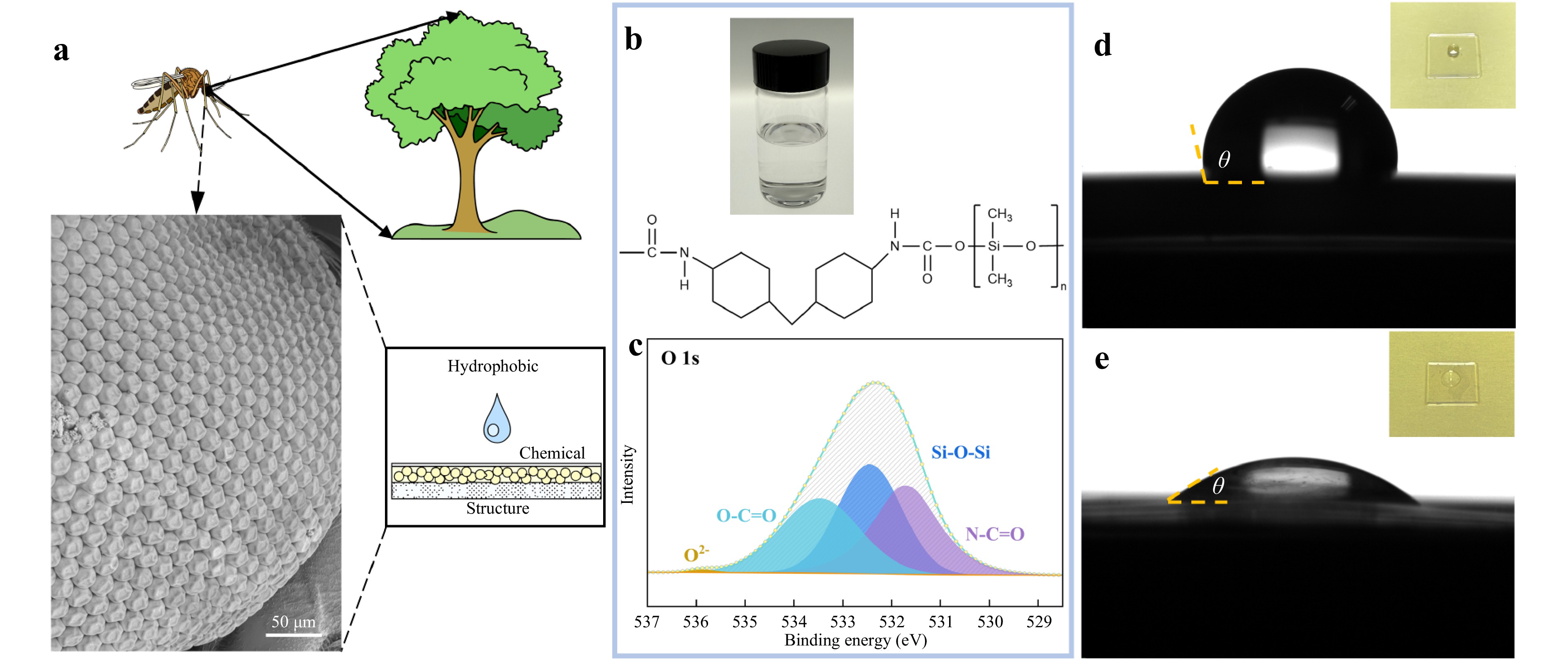
Fig. 1 Design inspiration of the mosquito-eye-inspired hydrophobic metalens. a Bio-inspiration from a mosquito's compound eye. The left panel shows SEM images of a mosquito compound eye (scale bar, 50 μm). b A photograph of the UV-curable hydrophobic polymer material used for nanoimprint, along with its chemical structure. c High-resolution XPS spectrum of the O 1s peak from the hydrophobic metalens surface. d, e Contact angles of the hydrophobic and hydrophilic metalens, respectively. The inset shows a photograph of those samples.
As a proof of concept, to fabricate a polarization-independent metalens that integrates both surface hydrophobicity and an optical focusing function, a precision molding technique based on NIL was employed in this work. The specific fabrication process is illustrated in the schematic in Fig. 2a. The pattern from a master stamp is replicated onto a flexible material via a hot-pressing process to create a secondary stamp. The TOPAS film was selected as the substrate for the secondary stamp. The relatively low glass transition temperature (Tg = 78°C) enables the high-precision replication of nanostructures from the master stamp onto the TOPAS film under milder conditions. Subsequently, hydrophobic resin was spin-coated onto this TOPAS stamp and then cured by irradiation with 365 nm UV light, completing one NIL fabrication of the metasurface. The resin's chemical structure was confirmed by Fourier-transform infrared spectroscopy, which revealed characteristic absorption bands for N-H stretching (3,356 cm−1) and C-H stretching (2,850−3,000 cm−1). An intense, sharp peak at 1,719 cm−1 was attributed to C=O (carbonyl) stretching from the polyurethane and acrylate moieties, accompanied by an N-H bending vibration at 1,538 cm−1. Crucially, strong absorption bands in the fingerprint region at 1,090 cm−1, 1,020 cm−1, and 806 cm−1 are characteristic of Si-O-Si and Si-O-C asymmetric stretching, confirming the siloxane backbone58. The combination of these peaks confirms the material is a silicone-modified polyurethane acrylate composite resin.
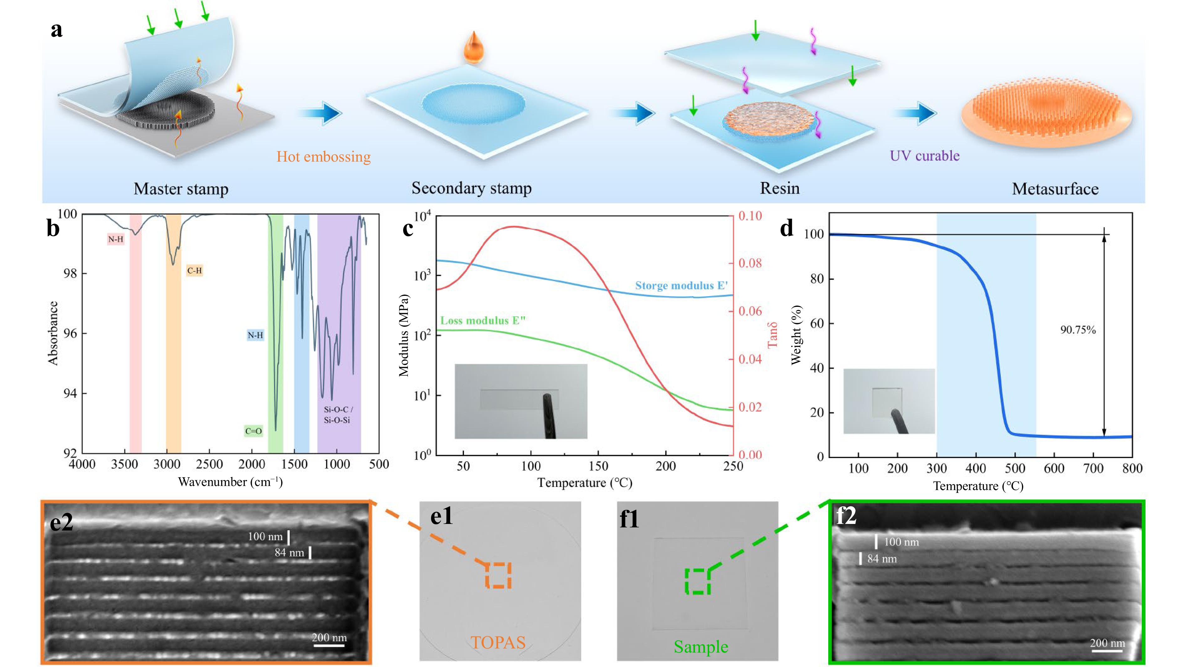
Fig. 2 Fabrication and characterization of the hydrophobic metalens. a Schematic of the fabrication of the metalens using NIL technology. b-d Fourier-Transform Infrared Spectroscopy spectrum, Dynamic Mechanical analysis, and Thermogravimetric analysis curve of the hydrophobic resin, respectively. e1, e2 Image and SEM result of TOPAS obtained through hot embossing, respectively. f1, f2 Image and SEM result of the sample obtained through NIL technology, respectively.
Thermodynamic properties are essential for assessing material stability, processability, phase behavior, and performance, guiding device optimization and design. The Dynamic Mechanical analysis (DMA) results indicate sluggish chain segment motion between 70°C and 130°C, which manifests as a broad glass transition temperature range for the material. This is evident in the DMA as an inconspicuous step decrease in the storage modulus $ \mathrm{E'} $, and a broad peak in the loss factor $ tan\delta $. This behavior is also reflected in the loss modulus $ \mathrm{E''} $, which shows a correspondingly broad peak in the same temperature range in Fig. 2c. And in the DSC curve as a wide endothermic step in Fig. S3. Furthermore, Thermogravimetric Analysis (TGA) was performed to assess the resin's thermal stability, as shown in Fig. 2d. The material exhibits thermal stability up to approximately 300°C with the primary mass loss occurring between 300°C and 550°C. The total weight loss upon heating to 800°C is approximately 90.75%, which is mainly attributed to the thermal cleavage of the organic segments of the resin, such as the polyurethane and acrylate components. To validate that the NIL technique, in conjunction with the hydrophobic resin, is capable of fabricating nanoscale features, we initially imprinted simple rectangular nanostructures by this process. Fig. 2e1, f1 show the TOPAS stamp and the final sample fabricated with the hydrophobic resin, respectively. As evidenced by their corresponding SEM results (Fig. 2e2, f2), the nanostructures were successfully transferred from the stamp to the sample, these results demonstrate that the process can reliably achieve a fabrication resolution below 100 nm. The high structural integrity and dimensional uniformity over large-area patterns are further detailed in Figs. S4 and S5. The sustainability of the NIL process is further highlighted by the reusability of the master stamp, as detailed in Fig. S6.
To further validate the potential of NIL for manufacturing optical elements with subtle height variations, the spiral stamp has been employed to fabricate a sample capable of generating donut-shaped beam. A series of characterizations were conducted to ensure the replication fidelity of the VPP sample and evaluate its optical performance. A Mach-Zehnder interferometer (MZI), depicted in Fig. 3a, was constructed to demonstrate the phase modulation capabilities of VPP sample. In this system, a coherent laser source is divided by the first beam splitter (BS) into two coherent paths, a sample arm (purple path) and a reference arm (green path). The NIL VPP sample is positioned in the sample arm. As the beam traverses this sample, it converts the initial Gaussian intensity profile into a "donut" shaped distribution with a central intensity null, as illustrated in the inset of Fig. 3a. Concurrently, the beam in the reference arm (green path) is guided by mirrors for the subsequent interferometric measurement. An image of the VPP sample presented in Fig. 3b, with insets showing results from Differential Interference Contrast (DIC) microscopy result (top right) and SEM image (bottom right). The successful replication of these structures via the NIL process strongly demonstrates the high Z-axis replication fidelity of this method for continuous surface profiles. The SEM image confirms that the imprinted surface is smooth and uniform, indicative of a high-quality replication process.
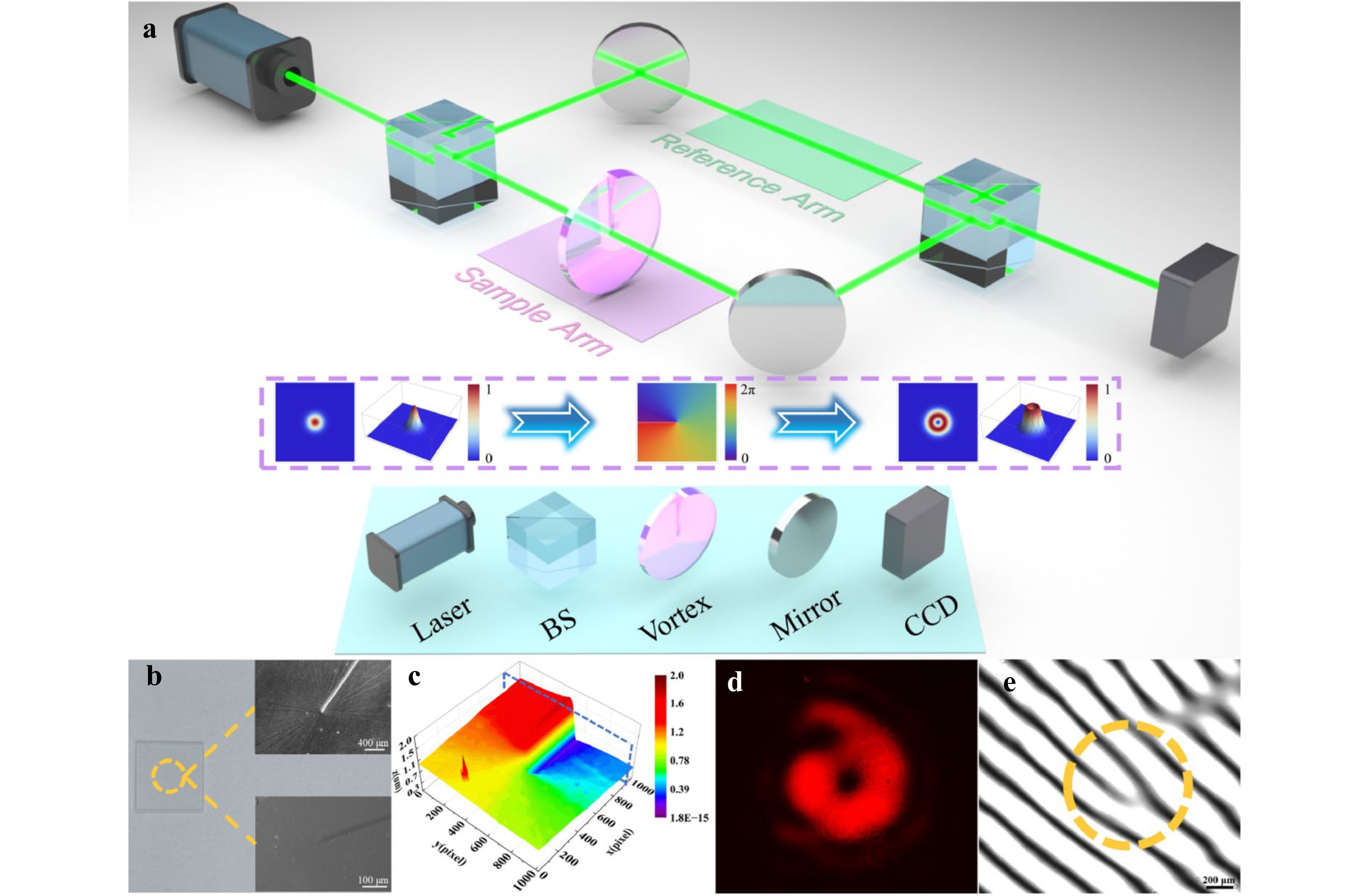
Fig. 3 Experimental characterization of the NIL VPP. a Schematic of the MZI setup used to characterize the VPP. The inset illustrates the light field evolution within the far-field sample arm. b Image of the fabricated VPP sample, with a DIC microscopy image (top right inset) and a SEM image (bottom right inset). c 3D surface profile of the VPP measured by a white-light interferometer. d Experimentally measured far-field intensity distribution after the beam passed through the VPP. e Interference pattern obtained from the setup in a.
The 3D morphology of the VPP sample was measured using a white-light interferometer (ZYGO) as shown in Fig. 3c. The resulting height map is analogous to a spiral staircase distribution. The maximum measured height difference across the structure was approximately 1.49 µm, which is in agreement with the design. Validation of the optical performance was conducted in two stages. First, a direct measurement of the far-field intensity distribution was performed. As shown in Fig. 3d, when the incident beam passed through the VPP sample, an annular intensity distribution was recorded in the far-field which is a signature of a vortex beam. To definitively confirm the integrity of its phase structure, the interferometric measurement was essential. The sample was placed within the MZI, allowing the modulated vortex beam to collinearly interfere with the reference beam at the second BS. The resulting interferogram captured by the CCD camera is presented in Fig. 3e. The forked fringe provides evidence of a topological charge of 1. This outcome demonstrates the capability of the above NIL scheme to achieve high-precision fabrication of optical elements featuring subtle, multi-level height variations.
The designed metalens stamp is composed of many tiny cylinders with different radii, the required phase profile for focusing is given by the formula $ \varphi \left(R,\lambda \right)=-\left[{2{\text{π}} }/{\lambda }\left(\sqrt{{R}^{2}+{F}^{2}}-F\right)\right] $, where $ \varphi $ is required phase distribution, $ \lambda $ is working wavelength, $ R $ and $ F $ represent the working distance and the focal length of metalens, respectively. The simulations results of the metalens have been summarized in Figs. S7 and S8. Fig. 4b displays an image of the hydrophobic metalens fabricated via the NIL described above, and its transparency corroborates the high transmittance property. The SEM result has been observed at low magnification (Fig. 4c) which reveals the layout of concentric annular. As the magnification is increased (Fig. 4d), the array of individual subwavelength nanopillars that constitute these zones can be clearly resolved. The results corresponding to Topas and sample of the metalens can be found in Fig. S9. A system in Fig. 4a was constructed to validate the optical performance of the metalens fabricated via NIL. A collimated laser (wavelength 532 nm) was used as the input source. It was followed by an absorptive density filter to prevent saturation of the CCD camera. The incident beam subsequently illuminates the metalens, which is followed by an objective used to magnify the minute light field distribution near the focal point. Finally, a CCD camera mounted on a high-precision motorized translation stage is responsible for acquiring the images that carry the light field intensity information. By scanning along the z-axis, a series of 2D light field slice images is collected and used to reconstruct the complete light field intensity distribution near the focus. The magnified intensity distribution obtained from the master stamp in the x-z plane (Fig. 4e1) shows the beam focus at the position of approximately 4.9 mm with white dashed line. At this position, the 2D and 3D point spread functions (PSFs) of the metalens are shown in Fig. 4e2, e3, respectively. These results further indicate that the focal spot with a compact energy distribution, which confirms that the theoretical design can achieve focusing. The hydrophobic metalens was tested in Fig. 4f. The result in Fig. 4f1 displays a focused beam with its focal length measured to be approximately 4.9 mm. Analysis of the PSF at the focal plane (Fig. 4f2, f3) reveals the background light intensity around the focal spot is low, indicating that the device possesses focusing efficiency. For subsequent imaging performance tests, a metalens fabricated from a hydrophilic resin but with an identical nanostructure geometry was used as the control in a comparative experiment (Fig. 4g). This hydrophilic metalens exhibited the strongest intensity measured at the white dashed line at approximately 4.9 mm (Fig. 4g1). The PSF at its focal plane (Fig. 4g2, g3) shows that the hydrophilic metalens also shows good focusing efficiency, which further demonstrates the reliability and repeatability of NIL for fabricating metalens.
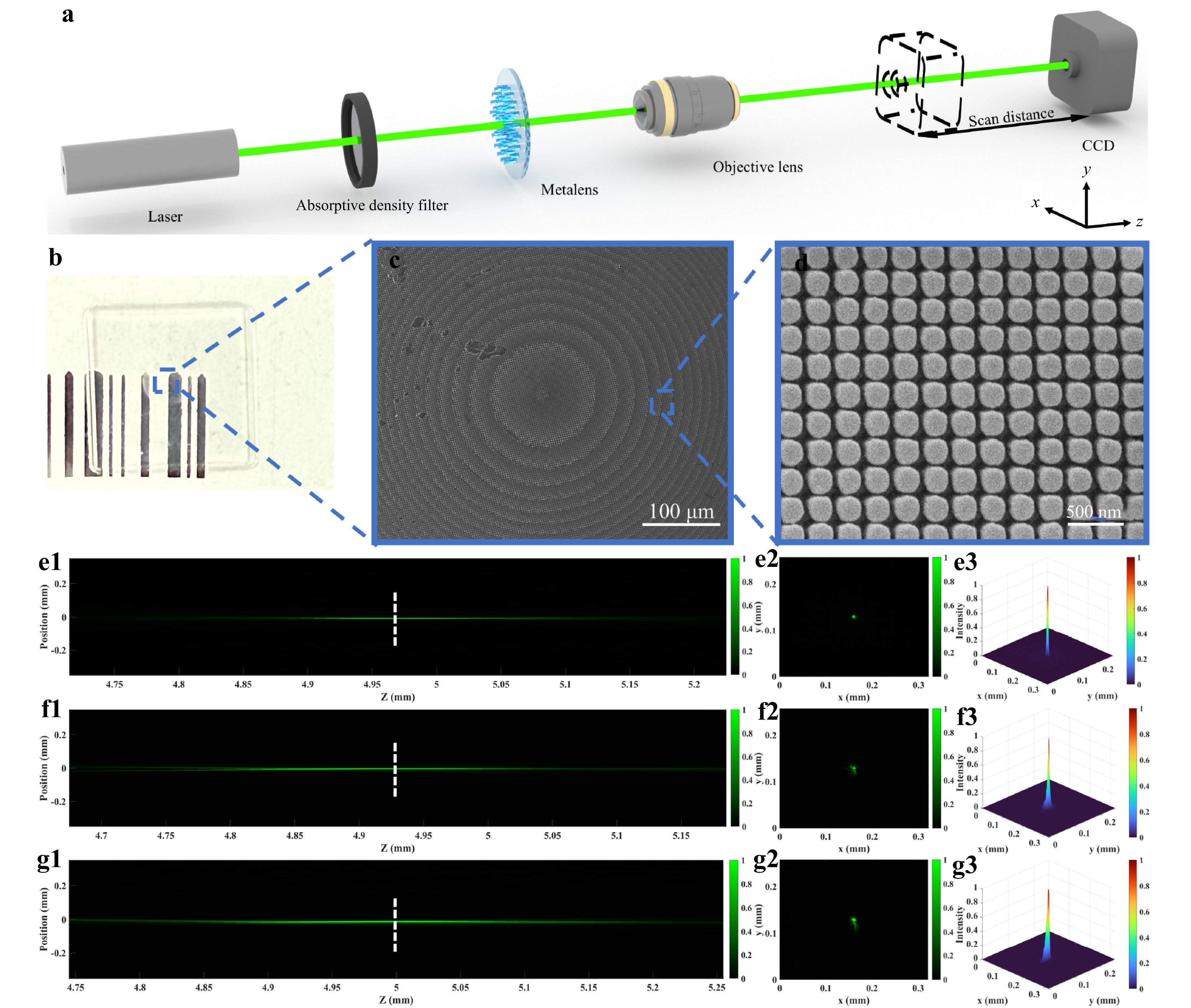
Fig. 4 Optical characterization of the fabricated metalens. a Schematic diagram of the optical path for collecting the light field distribution propagating along the x-z plane. b Image of the metalens sample. c SEM image of metalens (scale bar, 100 μm). d Magnified SEM image from c (scale bar, 500 nm). e1 The zoomed-in focusing profile of the metalens stamp. The measured focal length is 4.97 mm (white dashed line). e2, e3 The point spread function of the focal spot. f1-g3 The results of hydrophobic and hydrophilic metalens under the same measurements as e1-e3, respectively.
The anti-fouling ability of the fabricated hydrophobic metalens was investigated further after its optical focusing performance had been validated. The imaging principle for this experiment is shown schematically in Fig. 5a. When light from an object "META" on the object plane $ f(x,y) $ is incident on the metalens plane, each meta-atom on the surface radiates with a pre-designed hyperbolic phase profile. Finally, the light focusses on the image plane $ g(x,y) $, forming an image of "META". The hydrophobic metalens was evaluated in the blue-boxed region of Fig. 5. In uncontaminated state, the surface of the metalens is free of impurities, as shown in Fig. 5b1. It is capable of clearly resolving the target numbers "4" and "5" in Fig. 5b2, b3. Subsequently, its surface was rinsed with a suspension containing powder particles and then dried to simulate dust contamination in a real-world environment. After subjecting the contaminated lens to a single, simple rinse with deionized water, it was tested again. Remarkably, after just one cleaning, the majority of the impurities were washed off the surface of the hydrophobic metalens (Fig. 5c1), and its imaging capability was nearly indistinguishable from its original state (Fig. 5c2, c3), with the resulting image showing minimal differences in clarity and contrast compared to before contamination.
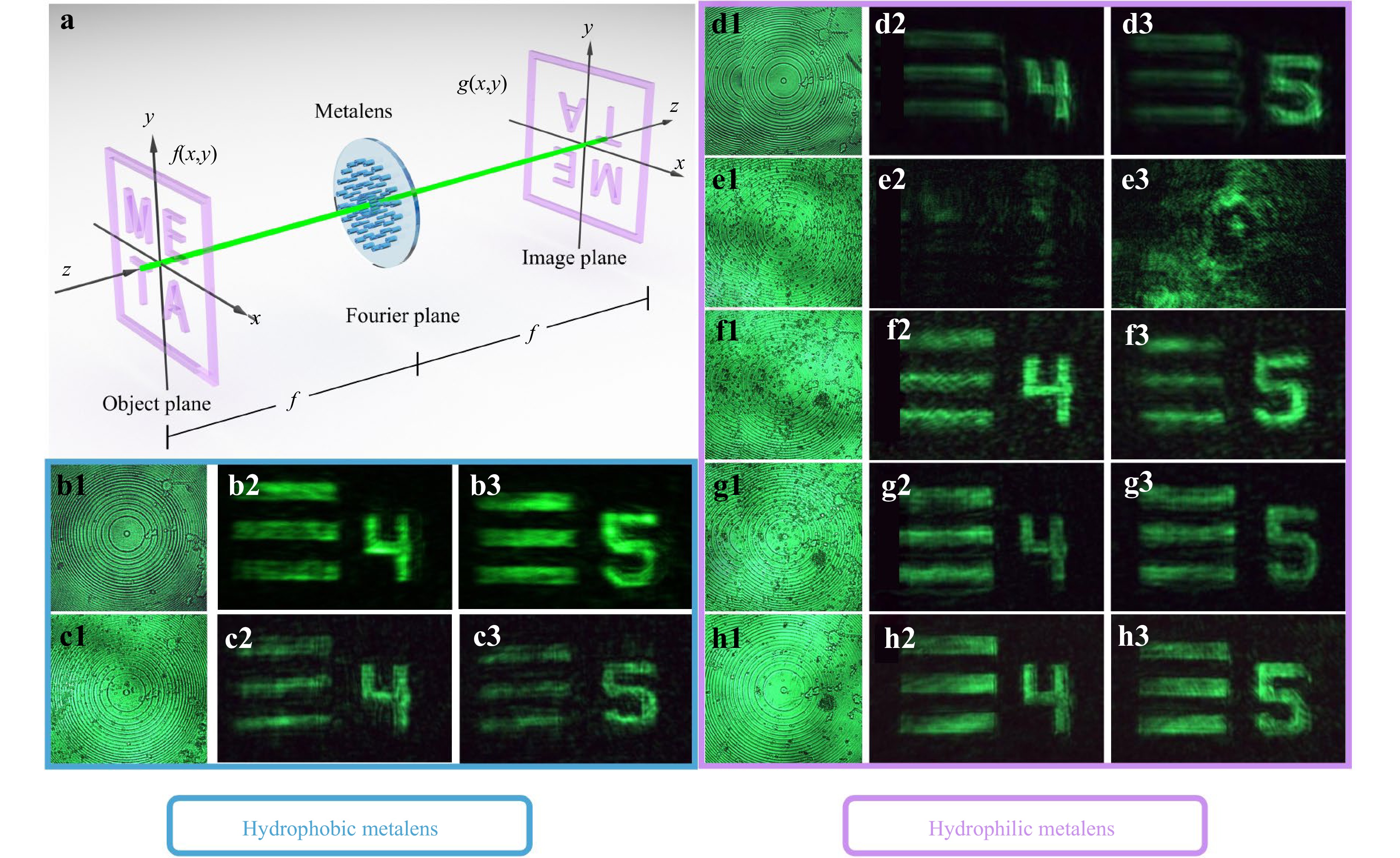
Fig. 5 Experimental imaging demonstration of the metalens. a Schematic of the metalens imaging system. b1-b3 The surface and imaging results of the hydrophobic metalens that have not undergone pollution source treatment. c1-c3 The surface and imaging results of the hydrophobic metalens that has been cleaned once. d1-d3 The surface and imaging results of hydrophilic metalens that have not undergone pollution source treatment. e1-h3 The surface and imaging results of the hydrophilic metalens that has been cleaned once, twice, a third and a fourth time, respectively.
In a control experiment, a surface image of the hydrophilic metalens was also free of impurities (Fig. 5d1) and possessed good imaging capabilities in its original state (Fig. 5d2, d3). However, after undergoing the same contamination and the first cleaning, a large number of contaminant particles remained firmly attached to its surface (Fig. 5e1), and the imaging quality suffered a catastrophic decline, with the image becoming extremely blurry and unrecognizable (Fig. 5e2, e3). The results showed that the imaging quality gradually improved with the number of cleanings, after the second cleaning (Fig. 5f), the image clarity improved significantly but it had not yet reached an ideal state. It was not until the third and fourth rinses with deionized water were completed (Fig. 5g, h) that the imaging quality of the hydrophilic metalens was finally restored to a level comparable to its original state. However, the phenomenon of localized aggregation and pinning of contaminants appeared on its surface. This phenomenon is particularly evident in the lower right corner of Fig. 5f1-h1. This contamination phenomenon is attributed to two primary mechanisms, where high surface energy enhances particle adhesion59 and the capillary force of receding water films concentrates particles into stable aggregates via a "coffee-ring effect"60. These comparative experiments thus demonstrate that the hydrophobic metalens possesses significant anti-fouling capability compared to its hydrophilic counterpart. This attribute is key to maintaining long-term high performance and stability in practical applications, especially in dusty, humid, or liquid-contact environments. Detailed analysis of the optical performance recovery is provided in Fig. S10. Furthermore, the long-term reliability of the metalens under UV exposure, thermal cycling, and chemical immersion is validated in Figs. S11-16.
Inspired by the mosquito eye, this work utilizes the NIL technique to fabricate hydrophobic metasurfaces with high precision. Specifically, a silicone-modified polyurethane acrylate is used as the fabrication material. Unlike conventional fabrication methods that struggle with cost and complexity, our proposed approach utilizes NIL to achieve high-resolution, sub-100 nm nanostructure fabrication. This technology introduces a scalable and cost-effective manufacturing method while ensuring the high-fidelity transfer of intricate optical patterns. The versatility of this approach was demonstrated by successfully fabricating a VPP with continues height variations and metalens with different diameter nanostructures. The optical characterization confirmed that the VPP generated the vortex beam with the intended topological charge. The experimental results demonstrate that the fabricated hydrophobic metalens possesses imaging capabilities. To investigate its durability in real-world application scenarios, we subjected it to an imaging capability test in a harsh environment, the hydrophobic metalens exhibits anti-fouling capabilities, preserving imaging quality where traditional hydrophilic devices fail. Its unique combination of anti-fouling functionality, high manufacturing precision, and low production cost makes it a key technology for next-generation optical systems. By bridging the gap between laboratory design and real-world durability, this bio-inspired strategy opens unique perspective for the application of metasurfaces in outdoor imaging, industrial sensing, and advanced consumer electronics.
-
This work was financially supported by the ECS scheme 21206223 and PolyU Startup grant.
Mosquito-eye inspired hydrophobic metasurface enabled by NIL with sub-100 nm resolution
- Light: Advanced Manufacturing , Article number: 92 (2026)
- Received: 29 December 2025
- Revised: 01 June 2026
- Accepted: 01 June 2026 Published online: 19 October 2026
doi: https://doi.org/10.37188/lam.2026.092
Abstract: Arthropods' remarkable ability to maintain clear vision in humid environments, owing to the water-repellent and anti-fogging properties of their compound eyes, provides significant inspiration for advancements in optical imaging technology. Metasurfaces, composed of periodically arranged optical nanostructures on a flat surface, can control the wavefront of incident light, leading to lighter and more compact optical integration. For metasurface, a hydrophobic surface is crucial for ensuring long-term operational stability when exposed to outdoor conditions. While protective or hydrophobic coatings can be integrated into metasurface designs by accounting for their refractive indices during the design phase, such coatings would reduce the refractive index contrast for devices based on low-index materials, which necessitate a substantial increase in the nanostructure height to achieve the required phase modulation, thereby increasing fabrication complexity and aspect-ratio requirements. Here, we introduce a method for fabricating low-cost and highly efficient hydrophobic metasurfaces using high-resolution nanoimprint lithography technology. As a proof-of-concept, the light field control capability of the hydrophobic spiral phase plate is demonstrated, the imaging capability of the hydrophobic metalens in harsh environments is explored, and their potential applications in advanced optical systems are demonstrated.
Research Summary
Nanomanufacturing: Nanoimprinting mosquito-eye inspired hydrophobic metasurfaces
Arthropods' remarkable ability to maintain clear vision in humid environments, owing to the water-repellent and anti-fogging properties of their compound eyes, provides significant inspiration for advancements in optical imaging technology. Metasurfaces are ultrathin optical components that can lead to lighter and more compact optical integration. For metasurface, a hydrophobic surface is crucial for ensuring long-term operational stability when exposed to outdoor conditions. Typically, adding protective or hydrophobic waterproof coatings to these devices complicates manufacturing and degrades their optical performance. Here, a method was introduced for fabricating low-cost and highly efficient hydrophobic metasurfaces using high-resolution NIL technology. As a proof-of-concept, the light field control capability of the hydrophobic spiral phase plate is demonstrated, the imaging capability of the hydrophobic metalens in harsh environments is explored, and their potential applications in advanced optical systems are demonstrated.
Rights and permissions
Open Access This article is licensed under a Creative Commons Attribution 4.0 International License, which permits use, sharing, adaptation, distribution and reproduction in any medium or format, as long as you give appropriate credit to the original author(s) and the source, provide a link to the Creative Commons license, and indicate if changes were made. The images or other third party material in this article are included in the article′s Creative Commons license, unless indicated otherwise in a credit line to the material. If material is not included in the article′s Creative Commons license and your intended use is not permitted by statutory regulation or exceeds the permitted use, you will need to obtain permission directly from the copyright holder. To view a copy of this license, visit http://creativecommons.org/licenses/by/4.0/.

 DownLoad: