






-
Lithography, the core process in semiconductor manufacturing, transfers mask patterns onto a wafer resist with high precision using an objective lens system1,2. Computational lithography (CL) combines the electromagnetic simulation of the lithography process with optimisation algorithms to accurately achieve wafer patterns with high fidelity to the designed layout. This capability compensates for exposure deviations while enhancing pattern density and yield, establishing CL as a critical enabler for shrinking advanced technology nodes3–5. Functioning as a core component of CL models, the mask model is responsible for rapidly and accurately characterising the physical interaction between electromagnetic waves and the mask structure, with the mask near-field distribution serving as its output6. Physical covariance is a key indicator for evaluating the mask model performance, and it requires the outputs of the model for identical mask layouts to be invariant under translation and rotation7. This characteristic not only reflects the inherent physics of mask electromagnetic effects, but also ensures consistent optimisation results for identical design patterns during resolution-enhancement flows, such as optical proximity correction8. For 193 nm deep ultraviolet (DUV) lithography, as the critical dimensions (CD) shrink to the 45 nm node and below, electromagnetic interactions with mask three-dimensional topography become increasingly complex and pronounced. This renders traditional Kirchhoff-based thin-mask approximations inadequate9,10. Concurrently, the development of inverse lithography technology (ILT) has broken free from the constraints of traditional ‘Manhattan’ mask layouts11–13. The adoption of all-angle edges significantly expands the process window while improving CD uniformity and sidelobe printing control14–16. Furthermore, the maturation of multibeam mask writing17 and the standardisation of curvilinear mask data formats18 have accelerated the industrial adoption of curvilinear masks19. In this context, developing thick-mask models that can efficiently and accurately characterise 3D electromagnetic effects on curvilinear mask layouts while maintaining physical covariance has become a pressing challenge in CL20.
Although rigorous numerical solutions to Maxwell’s equations, such as finite-difference time-domain (FDTD)21, rigorous coupled-wave analysis22, and waveguide23, can accurately resolve mask near-fields, they are computationally prohibitive for full-chip mask layouts owing to memory and runtime constraints. Various thick-mask approximation techniques have been developed to balance the accuracy and efficiency9,10. To exploit the translational and rotational invariance of electromagnetic effects, a common strategy involves extracting electromagnetic responses for a set of representative structures via rigorous simulation and then compositing these responses into near-rigorous full-chip models using the domain decomposition method (DDM)24. Alternatively, these rigorously simulated responses can be used to derive boundary corrections for the thin-mask model under the Kirchhoff approximation, such as the boundary layer model25 and edge-filter model9,26. Note that signal processing principles from other optical domains can inform the extraction of key electromagnetic responses in thick-mask modelling27. With the development of computer technology, deep-learning and machine-learning methods have been applied to develop efficient thick-mask models28–30. These thick-mask models predominantly address Manhattan geometries with a constrained orientation diversity. The growing adoption of curvilinear masks has considerably increased pattern complexity and introduced intricate diffraction effects that challenge traditional models in terms of efficiency, accuracy, and the preservation of physical covariance31. Early approaches to modelling curvilinear edges relied on Manhattanisation, in which curves were approximated by orthogonal segments, thereby incurring inherent geometric errors and degrading the physical covariance32. Subsequent Mask3D kernel models extract direction-dependent filter functions from rigorous simulations20,33,34; however, they still face fundamental challenges in achieving a real-time, physically covariant alignment of these kernels with arbitrarily oriented edges at full-chip scale. Table 1 compares representative thick-mask models to distinguish the present study from prior thick-mask modelling approaches.
Model Rigorous simulation based Mask pattern type Topology-decoupled kernel Explicit full-chip modelling framework Physically-covariant preserved DDM / edge-filter model √ Manhattan × √ × Manhattanisation-based model √ Curvilinear (approximated) × √ × Earlier Mask3D kernel model √ Curvilinear √ × × Proposed model √ Curvilinear √ √ √ Table 1. Comparison of representative thick-mask models
As shown in Table 1, DDM- and Manhattanisation-based models can support full-chip modelling by pre-characterising a finite set of edge orientations; however, their applicability is still fundamentally limited to Manhattan or discretised-orientation structures. The earlier all-angle Mask3D kernel model introduced a local response kernel decoupled from the layout topology; however, it did not explicitly establish a physically covariant full-chip modelling framework for arbitrarily oriented curvilinear edges. In summary, these common limitations indicate three key challenges: (1) extracting differential edge diffraction functions that are decoupled from specific mask geometries and thus adaptable to arbitrary curvilinear layouts; (2) establishing a physically covariant relationship between these differential edge diffraction functions and the curvilinear edges of arbitrary orientation to ensure model accuracy; and (3) achieving the rapid, full-chip reconstruction of the diffracted field while preserving the covariant relation to meet the computational efficiency requirements. Therefore, it is necessary to develop a novel framework to address these challenges effectively.
This paper introduces a physically covariant curvilinear thick-mask model based on edge diffraction correction for rapid full-chip layout simulation. Initially, a vectorial mask transmission matrix was introduced to characterise the electromagnetic wave propagation through the mask, and matrix transformations were used to establish the covariant relationship between the polarisation components and the curvilinear mask edges. By expanding the transmission matrix into a power series and truncating it, we formulated the mask model as a linear superposition of a thin-mask approximation term and an edge diffraction correction term. This expression establishes a diffraction-correction-based theoretical framework for a thick-mask model applicable to full-chip curvilinear layouts. Within this theoretical framework, by combining the projection-slice theorem35,36 with electromagnetic diffraction principles, we mathematically decompose the 1D edge diffraction responses obtained from rigorous simulations into 2D differential edge diffraction kernels (DEDKs). These kernels represent the intrinsic diffraction response of an elementary edge and are decoupled from the specific mask topologies. Furthermore, to address the angular dependence of these DEDKs, we exploited their rotational symmetry in the spatial domain to establish a real-time physical covariant mapping between the DEDKs and the curvilinear edges of arbitrary orientations. Accordingly, a nine-channel tensor convolution was used to perform the path integration of DEDKs along the curvilinear edges, enabling the rapid reconstruction of the full-chip mask diffraction term. This reconstructed term was subsequently applied to correct the Kirchhoff thin-mask approximation, yielding a physically covariant thick-mask model that enables the efficient and accurate simulation of curvilinear layouts. The combination of speed and accuracy renders this model highly valuable for resolution-enhancement techniques applied in the lithography of curvilinear masks.
-
In the CL framework, the primary role of the mask model is to characterise the transformation of the incident electromagnetic field vector $ {\left[E_{X}^{\rm{in}}\left(x,y\right),E_{Y}^{\rm{in}}\left(x,y\right)\right]}^{\text{T}} $ into the near-field output $ {\left[E_{X}^{\rm{out}}\left(x,y\right),E_{Y}^{\rm{out}}\left(x,y\right)\right]}^{\text{T}} $ after interaction with the mask structure. This physical process can be abstractly represented as
$$ \left[\begin{array}{c} E_{X}^{\rm{out}}\left(x,y\right)\\ E_{Y}^{\rm{out}}\left(x,y\right) \end{array}\right]=\left[\begin{array}{cc} M_{X}^{X}\left(x,y\right) & M_{X}^{Y}\left(x,y\right)\\ M_{Y}^{X}\left(x,y\right) & M_{Y}^{Y}\left(x,y\right) \end{array}\right]\left[\begin{array}{c} E_{X}^{\rm{in}}\left(x,y\right)\\ E_{Y}^{\rm{in}}\left(x,y\right) \end{array}\right] $$ (1) where (x, y) are the spatial coordinates on the mask plane, and the matrices $ \left[M_{X}^{X}\left(x,y\right),M_{X}^{Y}\left(x,y\right);M_{Y}^{X}\left(x,y\right),M_{Y}^{Y}\left(x,y\right)\right] $ constitute the spatially varying Jones matrix of the mask, serving as the polarisation-dependent mathematical model of the mask, denoted simply as M.
During the 3D mask–electromagnetic wave interaction, thick-mask effects originate primarily from complex electromagnetic boundary perturbations at the mask edges, in contrast to the simplified boundary assumptions of thin-mask models. By leveraging this physical mechanism, we propose a curvilinear thick-mask model that incorporates edge-diffraction corrections, thereby extending the conventional Kirchhoff thin-mask approximation. Specifically, the electromagnetic response of the mask to the layout pattern can be approximately decomposed as
$$ {\boldsymbol M}\left(x,y\right)={{\boldsymbol M}}_{0}[A\left(x,y\right)]+{\boldsymbol{M}}_{1}[\partial A\left(x,y\right)]+o({\boldsymbol{M}}_{\text{n}}[A(x,y)]) $$ (2) where M0[A(x, y)] is the thin-mask term representing the ideal geometric transmission and is an affine function of the mask area indicator function A(x, y). M1[∂A(x, y)] constitutes the first-order edge diffraction correction, whose accurate and efficient modelling presents the central challenge in the thick-mask model. This term depends on the vector field of mask edges ∂A(x, y), and can be obtained by integrating the rigorously simulated DEDK along the mask edges. The term o(Mn[A(x, y)]) captures the higher-order diffraction effects that depend on the mask pattern and involve complex spatial interactions. In principle, such higher-order contributions can be obtained through rigorous simulations. Given the high-frequency cut-off imposed by the numerical aperture (NA) of the projection lens and the inherently small amplitude of this term, and in accordance with mainstream approximate thick-mask modelling practices20,33, higher-order diffraction effects are omitted to balance computational efficiency with accuracy. As the CD continues to shrink, higher-order diffraction contributions, such as coupling effects between adjacent mask edges, may become more pronounced. Nevertheless, owing to the inherently scalable architecture of the model, such higher-order effects can be incorporated in a manner analogous to the first-order edge correction. The corresponding higher-order diffraction kernels were extracted from rigorous simulations of masks with various CDs via 1D projection-slice and circular harmonic decomposition techniques, and a similar path-integral procedure was then applied to quantify their influence, thereby progressively improving the predictive accuracy.
Within the thick-mask modelling framework established in Eq. 2, the thin-mask component M0[A(x, y)] is directly mapped from the mask layout and is defined as
$$ {{\boldsymbol M}}_{0}[A\left(x,y\right)]=\begin{cases} {{t}}_{\text{bright}}{I},A\left(x,y\right)\in \mathrm{clear}~\mathrm{region}\\ {{t}}_{\text{dark}}{I},A\left(x,y\right)\in \mathrm{otherwise} \end{cases} $$ (3) where I is a 2 × 2 identity matrix, and tbright and tdark represent the complex transmission coefficients of the bright and dark regions, respectively. These coefficients can be obtained either experimentally or theoretically using the thin-film transfer-matrix method37. The edge diffraction correction term M1[∂A(x, y)] in a thick-mask model depends not only on the material properties of the mask but also on the local orientation of each edge segment. The efficient construction of this term with high accuracy for curvilinear masks is critical for ensuring the computational accuracy and efficiency of the proposed model, and will be the focus of our subsequent theoretical development.
-
We represent the edge correction term M1[∂A(x, y)] as an integral of the DEDK along the mask edges to attain sufficient geometric freedom for full-chip curvilinear masks. Here, DEDK is a mathematical construction that describes the diffraction response induced by a differential edge segment and cannot be directly measured or simulated in isolation. Instead, subtracting the thin-mask component from a rigorous straight-edge simulation yields a 1D projection of the kernel along the edge direction. According to the projection-slice theorem, the Fourier transform of this projection provides a central slice through a 2D kernel spectrum35. Guided by Huygens’ principle, we regard the differential edge as a rotationally covariant secondary source so that, in the edge-aligned local coordinate system, the induced radially symmetric response is independent of the absolute orientation of the edge, and a single normal slice is sufficient to recover the full radial spectrum. Because of the vectorial nature of the electromagnetic boundary conditions, we decomposed the frequency-domain slices into even and odd components. The even and odd parts of the DEDK were reconstructed using zero- and first-order circular harmonic transforms, capturing the scalar radial response and antisymmetric normal modulation, respectively. Their superposition reconstructed the complete kernel spectrum, which was then inverse-transformed into a spatial domain. This approach avoids repeated rigorous simulations for varying mask geometries, and provides the necessary flexibility to support the proposed curvilinear thick-mask model.
This model employs Maxwell-equation rigorous solvers to analyse the near-field response of the isolated thick-mask edge, thereby obtaining the edge diffraction response for specified geometric configurations. The edge diffraction response depends on the incident conditions and is typically expressed as a polynomial expansion of the incident wave vectors (kx, ky)38,39. As this study focused on developing an efficient and physically covariant curvilinear thick-mask model for a full-chip layout, we retained only the zeroth-order term of this expansion under the normal-incidence assumption. The remaining higher-order terms followed a similar construction and are therefore not elaborated here. Under an X-polarised plane wave $ {\boldsymbol E}_{{X}}^{\text{in}}={\left[1,~0\right]}^{\text{T}} $, the transmitted electric field yields the Jones matrix components $ M_{X}^{X}(x,y) $ and $ M_{Y}^{X}(x,y) $. Similarly, the Y-polarised incidences $ {\boldsymbol E}_{{Y}}^{\text{in}}={\left[0,\;1\right]}^{\text{T}} $ provide $ M_{X}^{Y}(x,y) $ and $ M_{Y}^{Y}(x,y) $. Fig. 1a depicts the simulations performed for the template of an infinitely long straight-edge mask structure with its surface normal points along the +x-axis. The rigorously computed electromagnetic near-field distribution in Fig. 1b demonstrates that the geometric symmetry constraints reduce the mask response to 1D functions $ L_{X}^{X}(x) $ and $ L_{Y}^{Y}(x) $ along the x-axis, which represent co-polarised responses under X- and Y-polarised illumination, respectively, whereas the cross-polarised components $ L_{Y}^{X}(x) $ and $ L_{X}^{Y}(x) $ vanish. Consequently, the Jones matrix can be simplified to a diagonal form. According to Eq. 2, the mask response M(x) is subtracted from the thin-mask term M0(x), as shown in Fig. 1c, and the edge-diffraction term M1(x) is isolated, as shown in Fig. 1d.
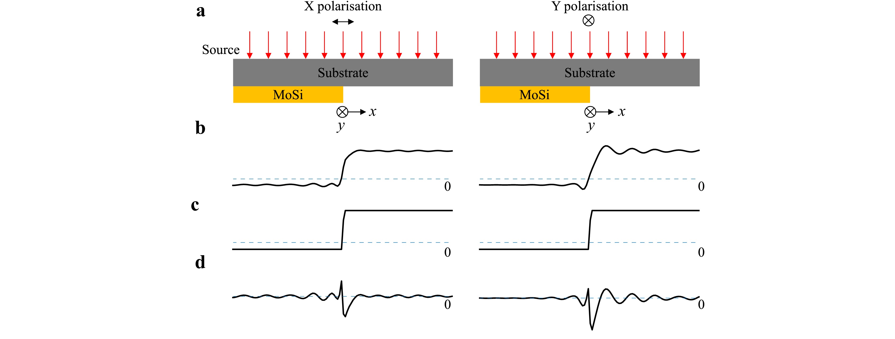
Fig. 1 Near-field characteristics of a template phase shift mask (PSM) structure under polarised illumination. a Template PSM structure with surface normal along the +x direction, illuminated by normally incident X- and Y-polarised sources. b Rigorous mask near-field distributions under X- and Y-polarised illumination. Simulation with sufficiently large periodicity to suppress edge coupling diffraction. c Thin-mask term $ L_{0,i}^{i}(x) $, calculated via multi-layer transfer matrix method. d Edge diffraction terms $ L_{1,i}^{i}(x) $.
Here, the 1D edge diffraction term $ L_{1,i}^{i}(x) $ represents the projection of the DEDK $ M_{1,i}^{i}(x,,y;\text{dy}) $ along the y-direction. By applying the projection-slice theorem, which characterises the Radon transform behaviour in the Fourier frequency domain35,36, we derived their relationship in the frequency domain:
$$\begin{split}& {\bf{FFT}}\left\{M_{1,i}^{i}\left(x,y;\text{dy}\right)\right\}\left(fx,fy=0\right)=\\&\quad{\bf{FFT}}\left\{L_{1,i}^{i}\left(x\right)\right\}\;\underline{\underline{\mathrm{def}}}\;\tilde{L}_{1,i}^{i}\left(fx\right),i={X,Y} \end{split}$$ (4) The Fourier spectrum of the edge diffraction term $ \tilde{L}_{1,i}^{i}\left(fx\right) $ is mathematically identical to the cross-section of the Fourier transform $ {\bf{FFT}}\left\{M_{1,i}^{i}\left(x,y;\text{dy}\right)\right\} $ at fy=0. To construct the diffraction kernel generated by the differential edge, the odd–even decomposition method is applied to the spectrum of the edge diffraction term $ \tilde{L}_{1,i}^{i}\left(fx\right) $, dividing it into two parts: an even component $ \tilde{L}_{1,i}^{i,e}\left(fx\right) $ representing the static background field (DC transmission term), and an odd component $ \tilde{L}_{1,i}^{i,o}\left(fx\right) $ that encodes the diffraction modulation along the edge normal. According to Huygens’ principle, each differential edge acts as a secondary source, emitting circularly symmetric diffraction perturbations. The Hankel transform reveals that circular symmetry is preserved under the Fourier transform20. Fig. 2 shows that the even-odd spectrum induced by the differential edge can be reconstructed by enforcing a circular symmetry operator, and the spatial diffraction field can be obtained using the inverse Fourier transform:
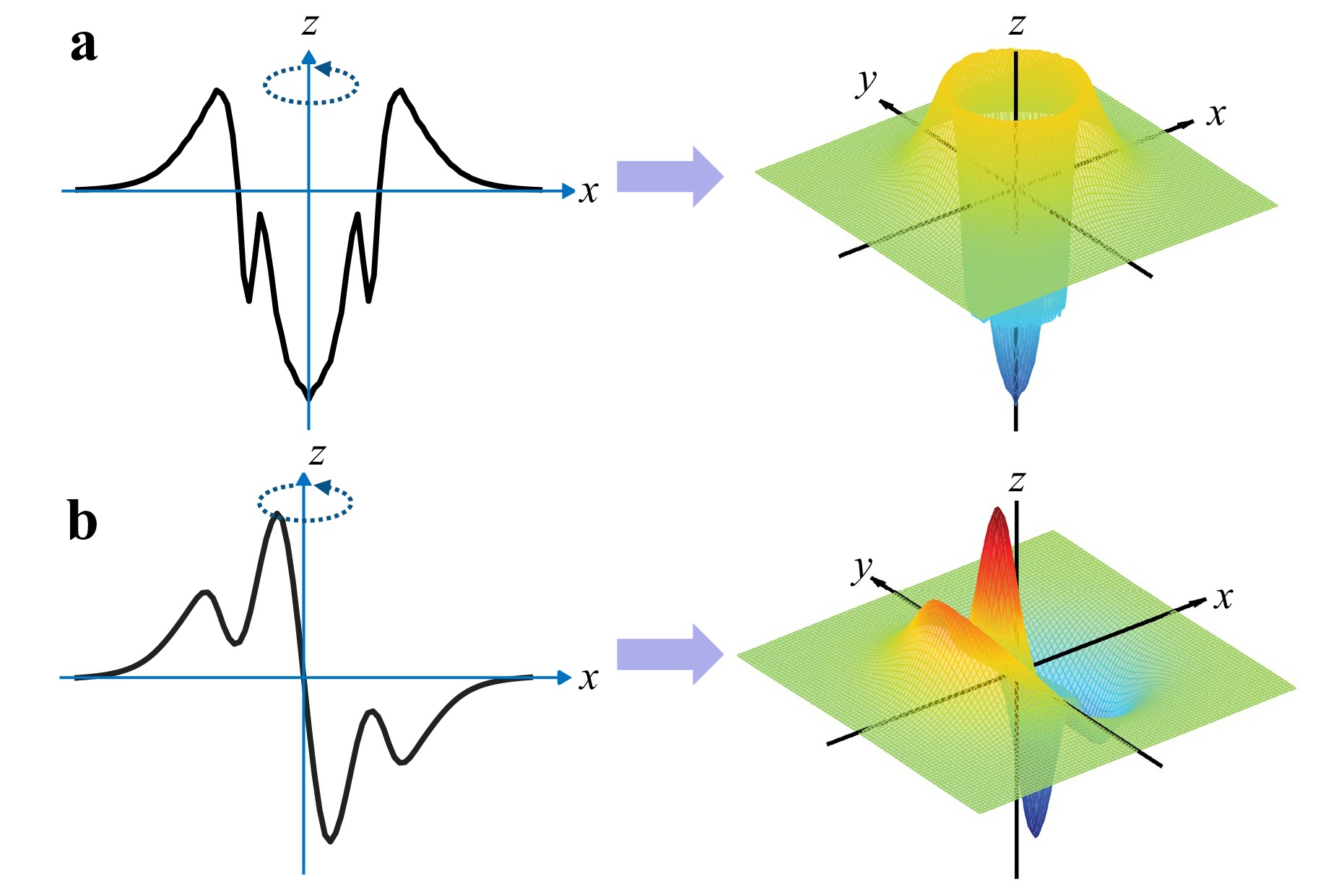
Fig. 2 Spectral reconstruction of even/odd components in the DEDK. a The left-side image illustrates the even spectral component $ \tilde{L}_{1,i}^{i,e}\left(fx\right) $. By performing axisymmetric rotation around the z-axis, the corresponding kernel even component spectrum is shown on the right. b The left-side image shows the odd spectral component $ \tilde{L}_{1,i}^{i,o}\left(fx\right) $. During rotation around the z-axis, an azimuthal modulation factor $ \cos \varphi $ is introduced, yielding the odd component spectrum in the right image.
$$ M_{1,i}^{i,e}\left(x,y;\text{dy}\right)={\bf{IFFT}}\left\{{\bf{circ}}\left(\tilde{L}_{1,i}^{i,e}\left(fx\right)\right)\right\},i={X,Y} $$ (5) $$ M_{1,i}^{i,o}\left(x,y;\text{dy}\right)={\bf{IFFT}}\left\{{\bf{circ}}\left(\tilde{L}_{1,i}^{i,o}\left(fx\right)\right)\cos \varphi \right\},i={X,Y} $$ (6) Here, $ M_{1,i}^{i,e}\left(x,y;\text{dy}\right) $ captures the scalar radial response, whereas $ M_{1,i}^{i,o}\left(x,y;\text{dy}\right) $ represents the antisymmetric modulation along the edge normal. circ() enforces circular symmetry; the x- and y- axes of the circular symmetry correspond to the normal and tangential directions of the long straight-edge used in the rigorous simulation, respectively. The angle $\varphi $ is measured in the frequency domain with respect to the edge normal direction (+fx axis).
Superimposing even components $ M_{1,i}^{i,e}\left(x,y;\text{dy}\right) $ and odd components $ M_{1,i}^{i,o}\left(x,y;\text{dy}\right) $ generates the DEDK M1(x, y; dy). This has an evident physical interpretation and is decoupled from the specific mask structure. This property strongly supports the construction of the curvilinear layout diffraction field M1[∂A(x, y)].
-
In curvilinear mask layouts, each local edge segment exhibits an arbitrary normal angle in the x–y plane. DEDK, which serves as a physical kernel describing electromagnetic diffraction phenomena, inherently satisfies translational and rotational invariances. Consequently, the differential diffraction response $ {\boldsymbol{M}}_{\bf 1}^{{θ}}\left(x,y;\text{dr}\right) $ for an infinitesimal edge segment with local normal angle θ relative to the x-axis satisfies the covariant transformation:
$$ {\boldsymbol{M}}_{\bf 1}^{{θ}}\left(x,y;\text{dr}\right)={\boldsymbol{R}}(-\theta ){\boldsymbol{M}}_{\bf 1}^{\bf{rot}}\left(x,y,\theta ;\text{dr}\right){\boldsymbol{R}}(\theta ) $$ (7) where R(θ) is the 2D rotation matrix, and $ {\boldsymbol{M}}_{\bf 1}^{\bf{rot}}\left(x,y,\theta ;\text{dr}\right)={\boldsymbol{M}}_{\bf 1}\left(x\cos \theta +y\sin \theta ,-x\sin \theta +y\cos \theta ;\text{dy}\right) $ represents the rotation of the spatial coordinate system of the diffraction kernel element. Fig. 3 depicts the covariant transform of the DEDK in the local in-plane edge normal direction.
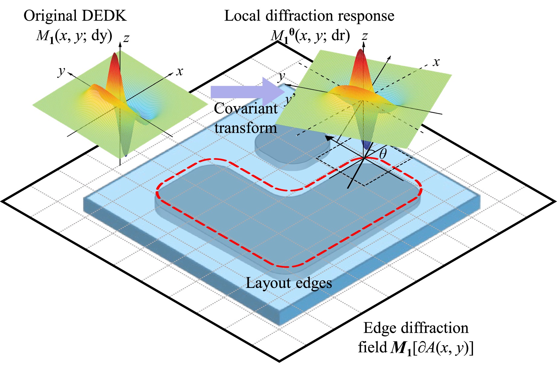
Fig. 3 DEDK transform in the differential edge-normal direction. Starting from the precomputed DEDK component M1(x, y; dy) corresponding to a template mask edge structure with its normal along the x-axis, curvilinear pattern edges are discretised into differential elements dr. For each element, the local normal angle θ is computed, and the local diffraction response $ {\boldsymbol{M}}_{\bf 1}^{{θ}}\left(x,y;\text{dr}\right) $ is derived through covariant transformation and superimposed at the position of the element in the diffraction field.
As discussed in the preceding section, the DEDK decomposes into two components: the even component characterises the static background field, which is insensitive to edge rotation; thus, its impact depends primarily on the edge segment length; and the odd component captures the edge-normal diffractive modulation, requiring rotational transformation to align with the local edge orientation for the accurate modelling of direction-sensitive diffraction effects. This per-element rotation significantly increases both the computational complexity and runtime demands owing to the geometric complexity of the full-chip curvilinear mask. Specifically, $ {\boldsymbol{M}}_{\bf 1}^{\bf{o}}\left(x,y;\text{dr}\right) $ is the odd component of the circularly symmetric directional kernel. Its rotation can be represented by a trigonometric combination of itself and its orthogonal diffraction modulation components, $ {\left[{\boldsymbol{M}}_{\bf 1}^{{o}}\left(x,y;\text{dr}\right)\right]}^{\text{T}} $. This enables real-time alignment between the kernel orientation and the edge geometry, thereby ensuring the physical covariance of the diffraction response. Accordingly, the rotated diffraction response of any differential edge with an angle of θ can be represented as the linear superposition of three field vectors:
$$ {\left(M_{1,i}^{i}\right)}^{rot}=M_{1,i}^{i,o}\cos \theta +{\left[M_{1,i}^{i,o}\right]}^{\text{T}}\sin \theta +M_{1,i}^{i,e},i=X,Y $$ (8) Combining Eqs. 7, 8, the local diffraction response $ {\boldsymbol{M}}_{\bf 1}^{{θ}}\left(x,y;\text{dr}\right) $ induced by a single edge segment at angle θ is expressed as
$$\begin{split}& {\boldsymbol{M}}_{\bf 1}^{{θ}}\left(x,y;\text{dr}\right)\\=\;&\left[\begin{array}{cc} \cos \theta & \sin \theta \\ -\sin \theta & \cos \theta \end{array}\right]\left[\begin{matrix} M_{1,X}^{X,rot} & 0\\ 0 & M_{1,Y}^{Y,rot} \end{matrix} \right]\left[\begin{matrix} \mathit{\cos } \theta & -\mathit{\sin } \theta \\ \mathit{\sin } \theta & \mathit{\cos } \theta \end{matrix} \right]\\ =\;&\left[\begin{array}{cc} \dfrac{{\left(M_{1}^-\right)}^{rot}}{2}\cos 2\theta +\dfrac{{\left(M_{1}^+\right)}^{rot}}{2} & -\dfrac{{\left(M_{1}^-\right)}^{rot}}{2}\sin 2\theta \\ -\dfrac{{\left(M_{1}^-\right)}^{rot}}{2}\mathit{\sin } 2\theta & -\dfrac{{\left(M_{1}^-\right)}^{rot}}{2}\mathit{\cos } 2\theta +\dfrac{{\left(M_{1}^+\right)}^{rot}}{2} \end{array}\right] \end{split}$$ (9) where the shorthand notations $ M_{1}^{-}=M_{1,X}^{X}\left(x,y;\text{dy}\right)- M_{1,Y}^{Y}\left(x,y;\text{dy}\right) $ and $ M_{1}^{+}=M_{1,X}^{X}\left(x,y;\text{dy}\right)+M_{1,Y}^{Y}\left(x,y;\text{dy}\right) $ are defined.
-
In the preceding section, we derived the diffraction field $ {\boldsymbol{M}}_{\bf 1}^{{θ}}\left(x,y;\text{dr}\right) $ generated by a differential edge at an arbitrary orientation. By performing the path integration of this field along all the mask edges, we constructed a full-chip covariant edge diffraction response M1:
$$ {\boldsymbol{M}}_{\bf 1}[\partial A\left(x,y\right)]={\oint}_{\text{edge}}{\boldsymbol{M}}_{\bf 1}^{{θ}}\left(x,y;{r}\right)\text{d}r $$ (10) To efficiently construct the edge correction term M1[∂A(x, y)] for full-chip curvilinear masks, we propose an algorithm that realises the path integral via nine-channel convolution, with reference to Eqs. 8, 9. The detailed implementation workflow is shown in Fig. 4.
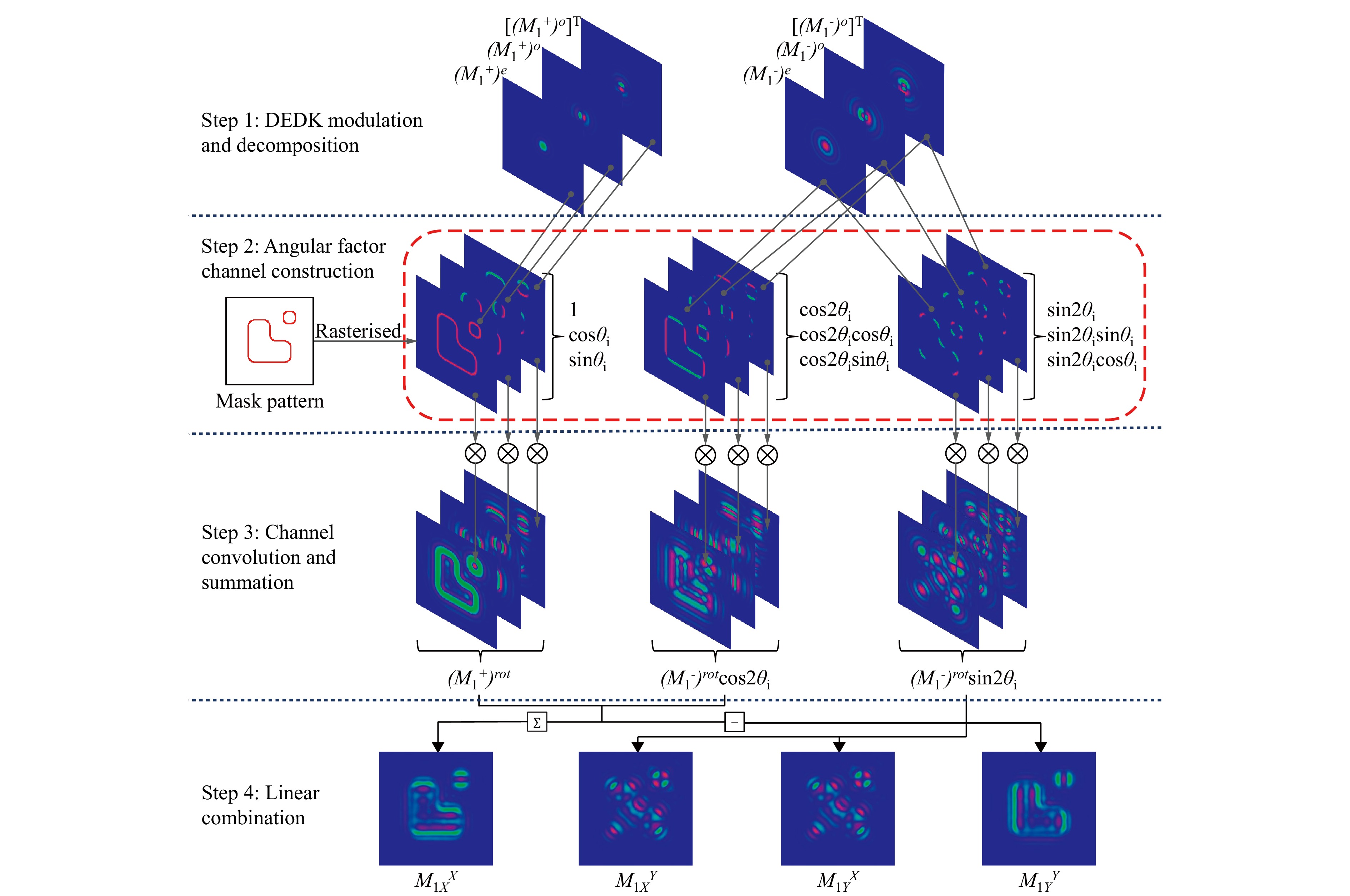
Fig. 4 Workflow of the nine-channel convolution algorithm for curvilinear mask path integration. Step 1: The DEDK undergoes a rotational similarity transformation and an adjoint rotation, and is decomposed into the basis set $ \left\{\left\{{\left(M_{1}^{+}\right)}^{e},{\left(M_{1}^{+}\right)}^{o},{\left[{\left(M_{1}^{+}\right)}^{o}\right]}^{\rm T}\right\};\{{\left(M_{1}^{-}\right)}^{e},{\left(M_{1}^{-}\right)}^{o},{\left[{\left(M_{1}^{-}\right)}^{o}\right]}^{\rm T}\}\right\} $. Step 2: The full-chip mask pattern is discretised. For each edge segment with a normal angle θi, the angular factors are computed and rasterised into nine image channels, formed by the tensor product {1, cos2θi, sin2θi}$\otimes ${1, cosθi, sinθi}. Step 3: The kernel set is convolved with the corresponding angular factor images, and the results are summed to obtain the full-chip Jones-matrix distribution components $ {\left(M_{1}^{+}\right)}^{rot},{\left(M_{1}^{-}\right)}^{rot}\cos2{\theta }_{i} $ and $ {\left(M_{1}^{-}\right)}^{rot}\sin2{\theta }_{i} $. Step 4: These components are linearly combined according to Eq. (9) to synthesise the edge correction term M1.
First, the DEDK Jones matrix was transformed by rotational similarity, yielding the modulated kernels $ M_{1}^{+} $ and $ M_{1}^{-} $. Simultaneously, the adjoint rotation of the modulated kernels was expressed as a linear combination of circular harmonic basis functions. Accordingly, the modulated kernels were decomposed into the following basis sets: $ \Big\{\left\{{\left(M_{1}^{+}\right)}^{e},{\left(M_{1}^{+}\right)}^{o},{\left[{\left(M_{1}^{+}\right)}^{o}\right]}^{\rm T}\right\};\{{\left(M_{1}^{-}\right)}^{e},{\left(M_{1}^{-}\right)}^{o}, {\left[{\left(M_{1}^{-}\right)}^{o}\right]}^{\rm T}\}\Big\} $. Subsequently, the full-chip mask edges were discretised. For each sufficiently short edge segment with a normal angle θi, the corresponding angular factors were rasterised into image channels. The angular factor channels consisted of the tensor-product combination of two sets of rotation representations: the Jones-matrix rotational similarity terms {1, cos2θi, sin2θi} and the adjoint rotation terms of the kernel {1, cosθi, sinθi}, resulting in nine channels. The kernel set was then convolved with the corresponding angular factor images and summed to obtain the full-chip Jones-matrix distribution components $ {\left(M_{1}^{-}\right)}^{rot}\cos 2{\theta }_{i} $, $ {\left(M_{1}^{-}\right)}^{rot}\sin 2{\theta }_{i} $ and $ {\left(M_{1}^{+}\right)}^{rot} $. Finally, these components were linearly combined to synthesise a full-chip edge diffraction correction term. This method accommodated the curvilinear edges of an arbitrary orientation, thereby overcoming the limitations of traditional Manhattanisation models that support only a few fixed directions, whereas the rotational similarity transformation of the Jones matrix guaranteed physical covariance. Moreover, by employing image convolution, the full-layout mask diffraction response could be rapidly constructed without explicit kernel rotation, thereby significantly improving modelling efficiency.
In the final synthesis stage, the edge diffraction term M1[∂A(x, y)] was superimposed with the thin-mask component M0[A(x, y)] to yield the complete curvilinear thick-mask model M(x, y), as illustrated in Fig. 5.
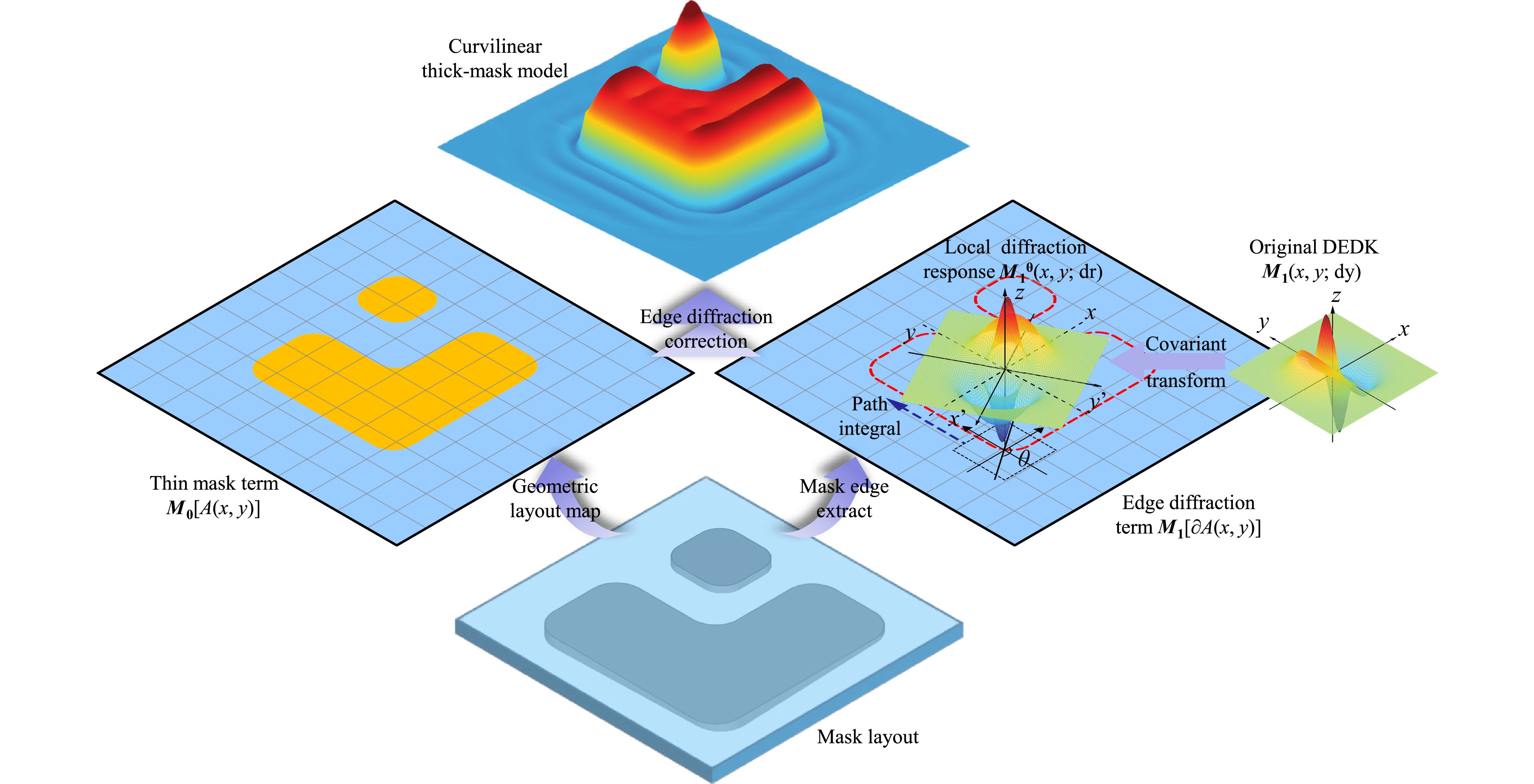
Fig. 5 Workflow for constructing a physically covariant curvilinear thick-mask model with edge diffraction correction. Starting from the mask layout, the thin-mask term M0[A(x, y)] is generated by mapping the geometric layout distribution. Geometric edges are then extracted, and the precomputed DEDK M1(x, y; dy) is loaded. For each differential edge segment dr with a normal angle θ relative to the x-axis, its diffraction response is computed using the covariance transform in Eq. 9. By integrating these local responses along the entire edge path, the physically covariant edge diffraction correction M1[∂A(x, y)] is assembled. Finally, the thin-mask term M0[A(x, y)] and the edge diffraction term M1[∂A(x, y)] are linearly superposed to form the curvilinear thick-mask model M.
This hierarchical approach ensured computational scalability while preserving the physical covariance for arbitrary edge orientations. By implementing nine-channel image convolutions to perform DEDK path integration along the mask edges, this method enabled efficient full-chip mask simulation. Consequently, it provided a physically covariant, rapid, and full-chip modelling solution for curvilinear masks, enabling accurate and efficient forward modelling for CL.
-
We quantified the accuracy of the proposed curvilinear thick-mask model by comparing the near-field amplitude distributions with the benchmark solutions obtained through rigorous FDTD simulations. To demonstrate the universality of the model, we applied it to both Manhattan structures and arbitrary curvilinear layouts and compared the deviation of each case against the FDTD reference.
The initial validation focused on the accuracy of the proposed model in simulating the Manhattan mask layouts. Fig. 6a shows the localised metal layer layout for the Manhattan geometries with a CD of 45 nm. Unless otherwise specified, all the mask dimensions mentioned in this study refer to the wafer scale. Using the $ {E}_{{X}}^{{X}} $ component generated under X-polarised illumination as an example, Fig. 6b shows the near-field simulation results for the Manhattan layout using the rigorous FDTD simulation, Kirchhoff thin-mask approximation, and proposed thick-mask models. Based on the simulation results, the Kirchhoff approximation yielded a root mean square (RMS) error of 0.1007 and a maximum absolute (MA) error of 0.8088, whereas the proposed model achieved an RMS error of 0.0336 and an MA error of 0.2901. These results demonstrate that the proposed model significantly enhances the accuracy of the thin-mask approximation, reducing both the RMS and MA errors by approximately 3×, thereby confirming its efficacy in simulating thick masks in Manhattan mask layouts.
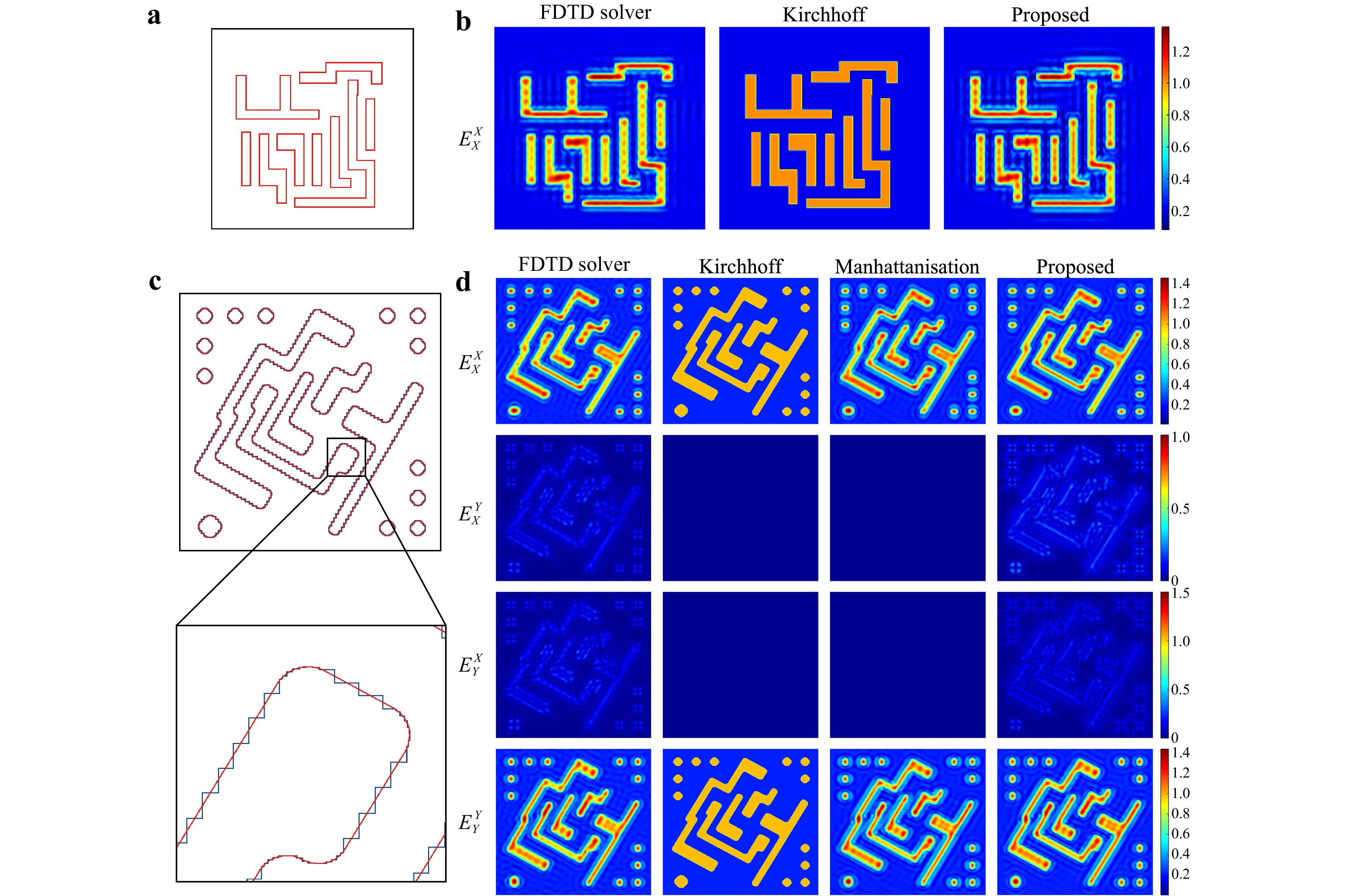
Fig. 6 Comparison of near-field modelling results for mask layouts via different modelling methods. a Manhattan mask layout with a CD of 45 nm. b Near-field distributions of the mask layout generated using the FDTD, thin-mask, and proposed models. c Curvilinear mask layout with a CD of 45 nm and its local magnification. The red line represents the original curvilinear mask geometry, composed of slanted segments and circular arc segments, characterised through discretised edge-sampling point sets. The blue line denotes the Manhattanisation layout, represented by orthogonal horizontal–vertical segments. d Near-field distributions of the curvilinear mask generated using the FDTD, thin-mask, Manhattanisation thick-mask, and proposed models.
Curvilinear masks represent the key application scenarios targeted by the proposed model. Simulation experiments validated the accuracy of the model in the near-field modelling of curvilinear mask layouts. Fig. 6c shows a typical curvilinear mask layout with a CD of 45 nm and its local magnified view. The mask layout comprised slanted edge segments and rounded corner curve segments, and was characterised by a discretised set of sampling points collected along the mask edges. Fig. 6d compares the near-field distributions across the four polarisation components of the curvilinear mask generated using the rigorous FDTD, thin-mask, Manhattanisation thick-mask, and proposed models.
The Manhattanisation thick-mask model approximates a curvilinear mask by breaking it into horizontal and vertical segments. The corresponding kernels were selected from a precomputed kernel library at the orientations of 0°, 90°, 180°, and 270°, convolved with the edge segments, and then linearly combined with the thin-mask term to produce the near-field distribution. To ensure a fair comparison, this model used the same rigorous simulation data source, thin-mask baseline, and kernel extraction method as the proposed model. The maximum edge displacement (MED), defined as the Hausdorff distance between the Manhattanised polygons and original curves, serves as a critical metric for evaluating the geometric fidelity after Manhattanisation and directly controls the accuracy of this approach40. The convergence curve of the near-field deviations in the Manhattanisation thick-mask model was simulated as the MED was varied, and the results are shown in Fig. S1 in the Supplementary Information. Based on the convergence curve, the MED for the Manhattanisation model was set to 4 nm.
Table 2 summarises the RMS and MA errors along with the run times for each method, using the rigorous FDTD results as the benchmark. The proposed model achieved a two times smaller RMS error compared with the Manhattanisation model while attaining a smaller MA error and faster run speed. Despite a run time approximately 5.5 times longer than that of the efficient Kirchhoff approximation method, the proposed model was dramatically faster than the rigorous FDTD approach, reducing the computation time by a factor of approximately 2,640. These results demonstrate the superiority of the proposed model for curvilinear masks, as it delivers higher numerical accuracy and computational efficiency than the existing thick-mask methods.
Model RMS error MA error Run time (s) FDTD ~6,895 Kirchhoff 0.1204 0.8288 0.4 Manhattanisation
(MED = 4 nm)0.0601 0.3445 2.73 Proposed 0.02858 0.2841 2.61 Table 2. Accuracy and efficiency metrics for mask modelling methods relative to FDTD
We compared deviations between the near-field distributions generated by the proposed model and benchmark FDTD simulations across various CDs and curvilinear mask layouts to validate the applicability of the proposed model, and the results are presented in Fig. S2 in Supplementary Information.
-
We imported the curvilinear mask near-field described in Fig. 6d into a Hopkins imaging system to quantitatively evaluate the impact of the mask model accuracy on the aerial image fidelity within the CL workflow41. Fig. 7a shows an X-polarised quadrupole illumination pupil, whereas Fig. 7b compares aerial images and deviations across different mask models, with the aerial image derived from the near field generated using FDTD as the benchmark. Table 3 presents the quantitative analysis results.
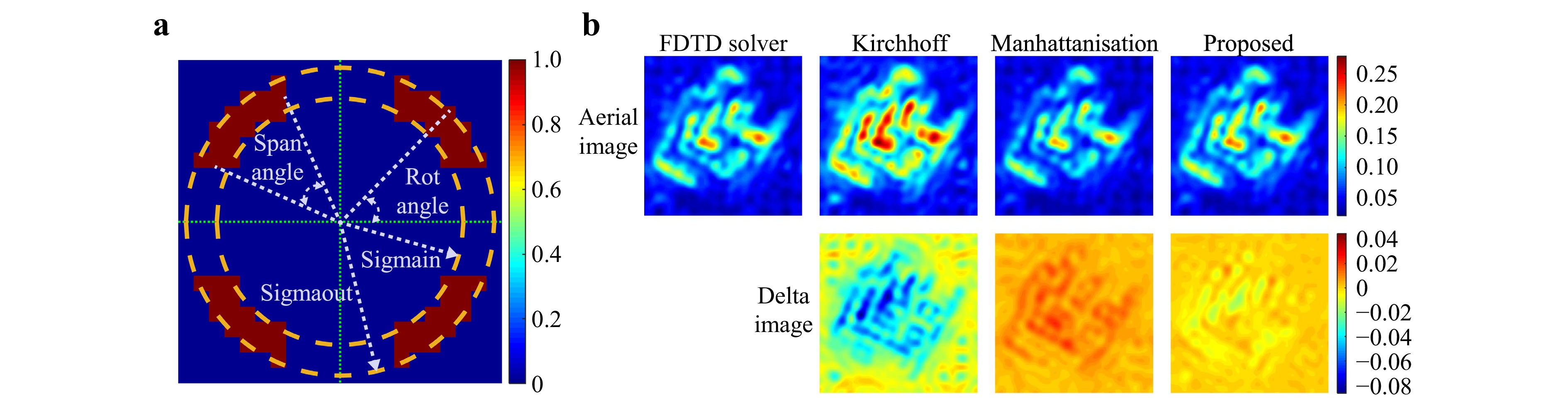
Fig. 7 Aerial image simulation and accuracy verification of curvilinear mask based on Hopkins imaging method. a Quadrupole illumination pupil with span angle = 45°, rot angle = 45°, sigmain = 0.8, sigmaout = 1.0. b Aerial images and comparison results generated using the Hopkins method under different mask models.
Model RMS error MA error Kirchhoff 0.02719 0.08666 Manhattanisation 0.006818 0.02233 Proposed 0.003297 0.01903 Table 3. Error metrics of aerial images relative to FDTD
Compared with the imaging results derived from the Kirchhoff and Manhattanisation mask models, the proposed method decreased the RMS error by 87.9% and 51.6%, respectively, and decreased the MA error by 78.0% and 14.8%, respectively. This comparative analysis demonstrates that the proposed curvilinear thick-mask model delivers superior imaging accuracy compared with existing models in a CL system.
-
Full-chip mask layouts frequently contain numerous repetitive units. Mask models must provide physically consistent representations of these units. This requirement is fundamental to semiconductor manufacturing and is governed by the principle of the physical covariance of electromagnetic effects. A key metric for assessing this property is the invariance of the model under coordinate transformations, which encompasses both translational and rotational invariances. Fig. 8a shows the workflow used to validate the physical covariance of the mask models. First, the near-field distribution N1 of the original mask layout was generated using the mask model as a reference. The mask layout was then subjected to an arbitrary coordinate transformation, such as translation or rotation, and re-simulated to obtain the near-field N2. The inverse transformation was applied to N2 to restore it to the original coordinates, yielding $ {\bf{N}}_{2}^{\text{'}} $. The deviation between N1 and $ {\bf{N}}_{2}^{\text{'}} $ quantitatively assesses the invariance of the model. Fig. 8b shows the test mask layout used in the experiment, which consisted of an array of rounded corner squares with a CD of 45 nm. The near-field distributions generated by translating or rotating the test mask are presented in the Supplementary Information (Fig. S3).
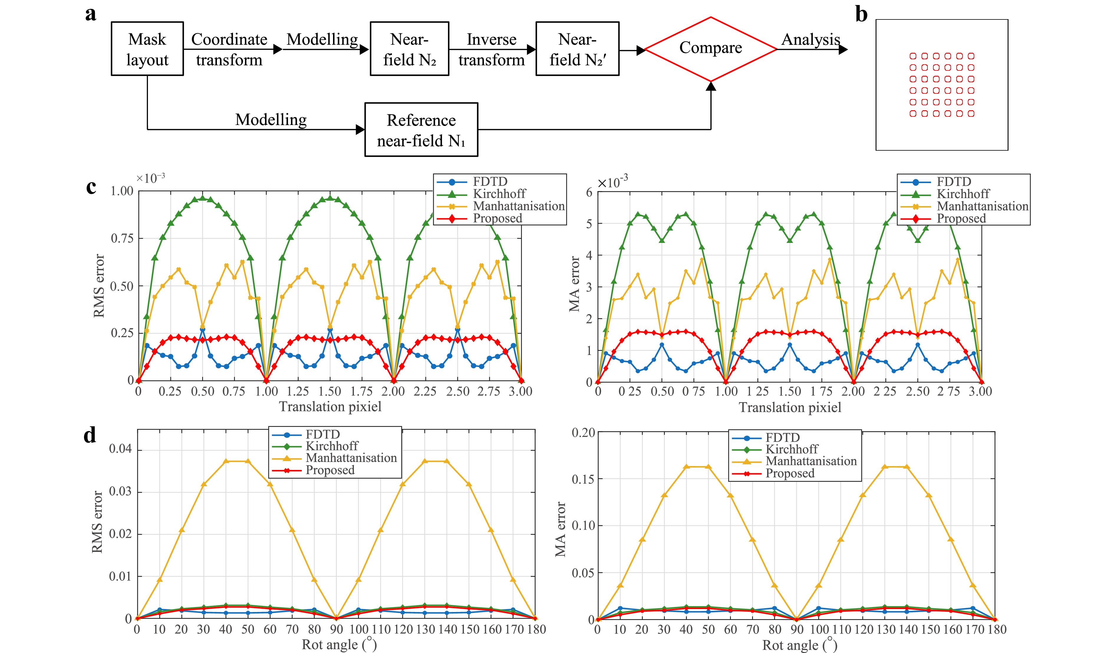
Fig. 8 Experiment for verifying the physical covariance of the mask models. a Workflow for the verification of the physical covariance of the mask models. b The test mask features an x–y symmetric layout and consists of an array of rounded-corner squares with a CD of 45 nm and a pitch of 90 nm. c RMS and MA errors vs. mask translation distance in the translational invariance test. d RMS and MA errors vs. mask rotation angle in the rotational invariance test.
Fig. 8c plots the RMS and MA errors of each model under translational invariance testing as a function of the mask translation distance. The curves reveal that the proposed model reduced both RMS and MA errors by approximately 70% relative to the Kirchhoff approximation while achieving accuracy comparable to that of rigorous FDTD simulations. These results validate the translational invariance of the proposed model, demonstrating that mask layout displacement has a negligible impact on its near-field predictions.
Fig. 8d shows the RMS and MA error as functions of the mask rotation angle in the rotational invariance test. An analysis of these curves indicates that the proposed model reduced both the RMS and MA errors by approximately 90% compared with the Manhattanisation thick-mask model, achieving rotational errors comparable to those of the rigorous physical model. These results validated the rotational invariance of the proposed model. Furthermore, the rotational errors approached zero at the orientations of 90° and 180°, revealing the exceptional symmetry-preservation capability of the proposed model.
-
The aforementioned experiments validated the performance of the proposed model in terms of accuracy, efficiency, and universality. For DUV lithography at the 45 nm node and below, the proposed model enabled the efficient construction of thick-mask near-field distributions that accurately reflect 3D mask topography. Compared with the existing Manhattanisation thick-mask model, the proposed model exhibited superior computational accuracy and efficiency when handling curvilinear mask layouts. This advantage originates from the fact that Manhattanisation requires a strict control of the MED across complex full-chip curvilinear mask layouts, which imposes additional computational overhead and introduces modelling errors. Furthermore, as explained in the principal section, the mask edge diffraction can be decomposed into even and odd field components, where the even component is scalar and dependent exclusively on the total edge length. As Manhattanisation alters the edge length (see Fig. 6c), it inevitably introduces an additional error term that degrades near-field modelling accuracy.
In terms of the validation of physical covariance, the rotational invariance test showed that the Manhattanisation model approximated curvilinear edges with horizontal–vertical segments, generating distinct geometric layouts at different rotation angles, thus breaking rotational invariance. By contrast, the proposed model extracted DEDKs and established a nine-channel tensor convolution architecture, achieving real-time covariant mapping between DEDKs and curvilinear edges at arbitrary orientations. This allowed the model to directly process curvilinear masks represented by discretised edge-sampling point sets, and it could be extended to other parametrically characterised geometries, termed ‘MULTIGON’18. By fundamentally avoiding Manhattanisation geometric approximations, the proposed model delivered higher predictive fidelity and achieved a physical covariance comparable to that of a rigorous physical model. Note that, in the translational invariance tests, the translation error of the model exhibited evident pixel-level periodic fluctuations. This indicated that the subpixel errors introduced by spatial discretisation remained a source of inaccuracy in the current model, warranting further reduction in future studies.
In summary, this paper proposed a physically covariant curvilinear thick-mask model based on edge diffraction correction for a rapid full-chip layout simulation. First, we expanded the mask transmission function into a series and truncated it into a linear combination of the thin-mask approximation term and an edge diffraction correction term. Through rigorous electromagnetic simulations, we derived physically meaningful 2D DEDKs and performed path integration along all the mask edges to reconstruct the full-chip edge diffraction term. Finally, this correction term was incorporated into the thin-mask approximation, yielding a rapid, physically curvilinear, thick-mask model. By comparing the near-field distributions across diverse mask layouts and quantifying the deviations between the generated aerial images and the benchmark, the proposed model achieved a 3× smaller error than the thin-mask model. Furthermore, the thick-mask model improved the computational efficiency by 2,640 times relative to the rigorous physical model, validating its efficiency and universality. In curvilinear layouts, our method avoided the geometric Manhattanisation errors of traditional thick-mask models, thereby significantly enhancing the accuracy while overcoming the degradation of physical covariance in mask electromagnetic effects. Furthermore, translational and rotational invariance tests confirmed that the proposed model achieved a 10× improvement in rotational invariance over the Manhattanisation model while maintaining a performance comparable to those of rigorous physical models, thereby validating its reliability. Thus, this model provides robust support for efficient and accurate forward modelling in CL resolution-enhancement techniques, such as ILT and source mask optimisation.
-
Simulation experiments were performed based on a standard phase-shift mask, and the material properties and geometric configurations are listed in Table 4. The thin-mask transmission coefficients tbright and tdark in Eq. 3 were calculated using the thin-film transfer matrix method using these parameters37. The same configuration was adopted for rigorous simulations.
Material n k Thickness (nm) Sidewall angle (°) SiO2 1.56 0 MoSi 2.43 0.6 69 90 Table 4. Phase-shift mask material and structural parameters
-
The experiments were conducted using a 193 nm immersion DUV lithography system equipped with 4× reduction optics and an NA of 1.35. To evaluate the accuracy of the model rigorously, the FDTD electromagnetic solver in ANSYS Lumerical was employed as a benchmark. Convergence analysis was performed for the FDTD benchmark to establish a gold standard reference. The simulations were set up with a discrete grid size of 4 × 4 × 2 nm on the mask scale, employing periodic boundary conditions in the xy-direction and perfectly matched layers along the z-direction.
A convergence test of the reference mask near-field versus the simulation domain size was performed to determine a sufficiently large simulation domain, as shown in Fig. 1b, and to eliminate edge-coupling effects. The results are shown in Fig. S4 in the Supplementary Information. To balance the computational cost and accuracy, a domain size of 18 wavelengths was chosen for the FDTD simulation and the extraction of DEDKs.
In the near-field simulation experiments shown in Figs. 6 and 8, the simulation region was 1,024 × 1,024 nm, corresponding to the wafer scale. The near-field image grid resolution for the thin-mask, Manhattanisation thick-mask, and proposed models was 4 × 4 nm at the wafer scale. The image size was 256 × 256 × 4, corresponding to the $ {E}_{{X}}^{{X}} $, ${E}_{{X}}^{{Y}} $, $ {E}_{{Y}}^{{X}} $, $ {E}_{{Y}}^{{Y}} $ components of the near field. For the FDTD simulations, rigorous simulations were performed under both X- and Y-polarisations to obtain the corresponding near-field components. Because of the reduction factor of the lithography system, the size of the FDTD near-field image was 1,024 × 1,024 × 4. The FDTD results were subsequently processed through frequency-domain resampling and served as a benchmark for evaluating the performance of the proposed model.
In the validation experiments of the physical covariance, the low-pass filtering characteristics of the lithographic system were considered32. All the near-field deviation results were filtered at the 2 × NA spatial-frequency cut-off to suppress high-frequency noise, enabling a focused comparison of the core CL model performance. In the translational invariance experiment, the curves in Fig. 8c were obtained by comparing the restored near-field distributions with those of the reference. Specifically, the test mask was translated to different positions along the x-direction under X-polarised illumination $ {E}_{{X}}^{\text{in}}={\left[1{,}0\right]}^{\text{T}} $, and the resulting near-field images were translated back to the initial position and compared with the reference. For rotational invariance validation, the mask near-field N1 manifested the physical covariant properties governed by Eq. 7. The curves in Fig. 8d were obtained by rotating the test mask to different angles α, generating near-field distributions under linearly polarised illumination $ {{E}}_{\text{in}}={\left[\cos \alpha ,\sin \alpha \right]}^{\text{T}} $, applying the inverse rotation to map the results back to the original coordinate system, and then comparing them with the reference near-field image.
All simulation codes were implemented in C++ and executed on a personal computer with Intel Core i7-10700 CPU, 2.90 GHz, 64.0 GB of RAM.
-
This study was supported by the National Natural Science Foundation of China (52130504 and 52205592), Major Program (JD) of Hubei Province (2025BEA006-4), Technology Innovation Program Project of Hubei Province (2024BAB013), and Major Program (JD) of Hubei Province (2023BAA008-2). The authors express their gratitude for the technical support provided by the Experiment Centre for Advanced Manufacturing and Technology at the School of Mechanical Science and Engineering at HUST. David H. Wei acknowledges productive discussions and collaborations with colleagues at Lanzhou University, where he provided a short course on lithography in July 2025.
Physically covariant, curvilinear thick-mask model for full-chip computational lithography
- Light: Advanced Manufacturing , Article number: 100 (2026)
- Received: 04 December 2025
- Revised: 09 June 2026
- Accepted: 10 June 2026 Published online: 23 September 2026
doi: https://doi.org/10.37188/lam.2026.100
Abstract: As semiconductor process nodes advance, the interaction between electromagnetic waves and mask three-dimensional topography becomes increasingly significant. Curvilinear masks with superior process windows are being rapidly adopted, exposing the limitations of existing thick-mask models in accommodating arbitrary curvilinear edges. Therefore, a theoretical framework for the full-chip-scale, rapid modelling of curvilinear thick masks is required. This paper introduces a physically covariant curvilinear thick-mask model based on edge diffraction correction for rapid full-chip layout simulation. The model decomposes the mask response into a thin-mask approximation term and an edge diffraction correction term. Through rigorous mathematical derivation, the diffraction response of the reference mask edges is decomposed into physically meaningful two-dimensional differential edge diffraction kernels. Furthermore, the edge diffraction term of full-chip layouts is efficiently reconstructed via a multi-channel tensor convolution framework, thereby correcting the thin-mask approximation and establishing the curvilinear thick-mask model. Simulation results demonstrated that, compared with finite-difference time-domain benchmarks, the proposed model achieved curvilinear mask near-field root mean square errors below 0.03 while delivering a speed-up of over 2,600 times. Moreover, it provided more than 2× error reduction over traditional Manhattanisation curvilinear models and maintained superior physical covariance. This study is expected to provide robust support not only for efficient and accurate forward modelling in resolution-enhancement techniques, such as inverse lithography technology and source mask optimisation, but also for the optical characteristic fast simulation of metasurfaces and metamaterials.
Research Summary
Computational lithography: Physically covariant, curvilinear thick-mask model
A new framework is proposed for full-chip near-field modelling of curvilinear thick masks by extracting differential edge diffraction kernels and using multi-channel image convolution. Conventional models rely on limited geometries and struggle with edges of arbitrary orientation. Shiyuan Liu and Hao Jiang at Huazhong University of Science and Technology, David H. Wei at Yuwei Optica Co., Ltd., and their colleagues derived universal kernels through rigorous simulation and mathematical analysis. The kernels are aligned in real time with full-chip curvilinear edges via multi-channel convolution, ensuring computational efficiency and strict physical covariance. Compared with finite-difference time-domain benchmarks, the method achieved a speed-up of over 2600 times without appreciable accuracy loss, while preserving physical covariance. This work offers a robust basis for efficient and accurate forward modelling in computational lithography.
Rights and permissions
Open Access This article is licensed under a Creative Commons Attribution 4.0 International License, which permits use, sharing, adaptation, distribution and reproduction in any medium or format, as long as you give appropriate credit to the original author(s) and the source, provide a link to the Creative Commons license, and indicate if changes were made. The images or other third party material in this article are included in the article′s Creative Commons license, unless indicated otherwise in a credit line to the material. If material is not included in the article′s Creative Commons license and your intended use is not permitted by statutory regulation or exceeds the permitted use, you will need to obtain permission directly from the copyright holder. To view a copy of this license, visit http://creativecommons.org/licenses/by/4.0/.

 DownLoad: