2021 Vol. 2, No. 3

Article
Model-based characterisation of complex periodic nanostructures by white-light Mueller-matrix Fourier scatterometry
Maria Laura Gödecke, Karsten Frenner, Wolfgang Osten
Published. 2021, 2(3) : 237-250 doi: 10.37188/lam.2021.018

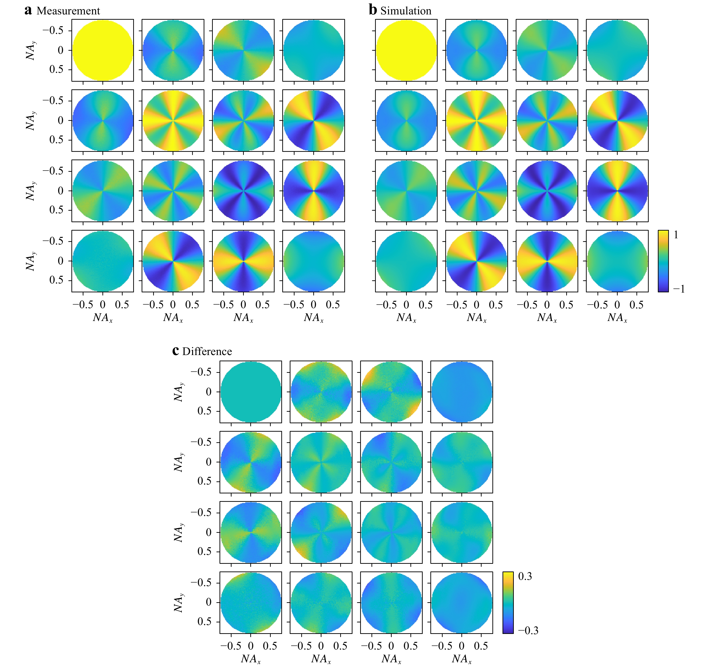
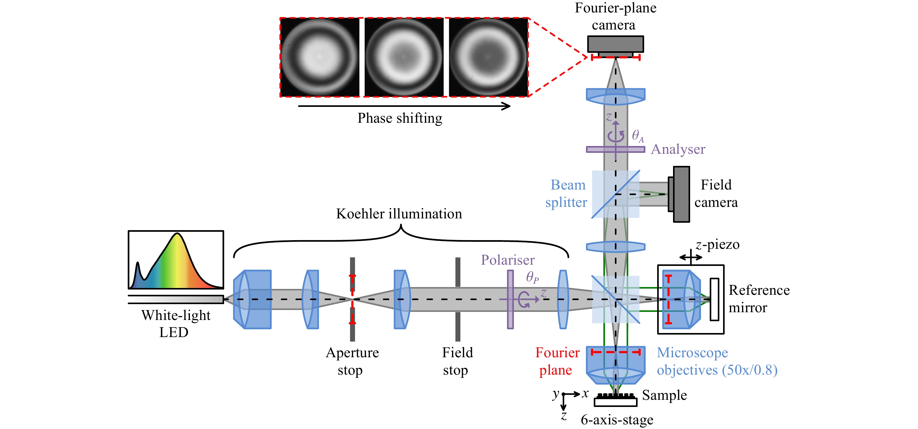
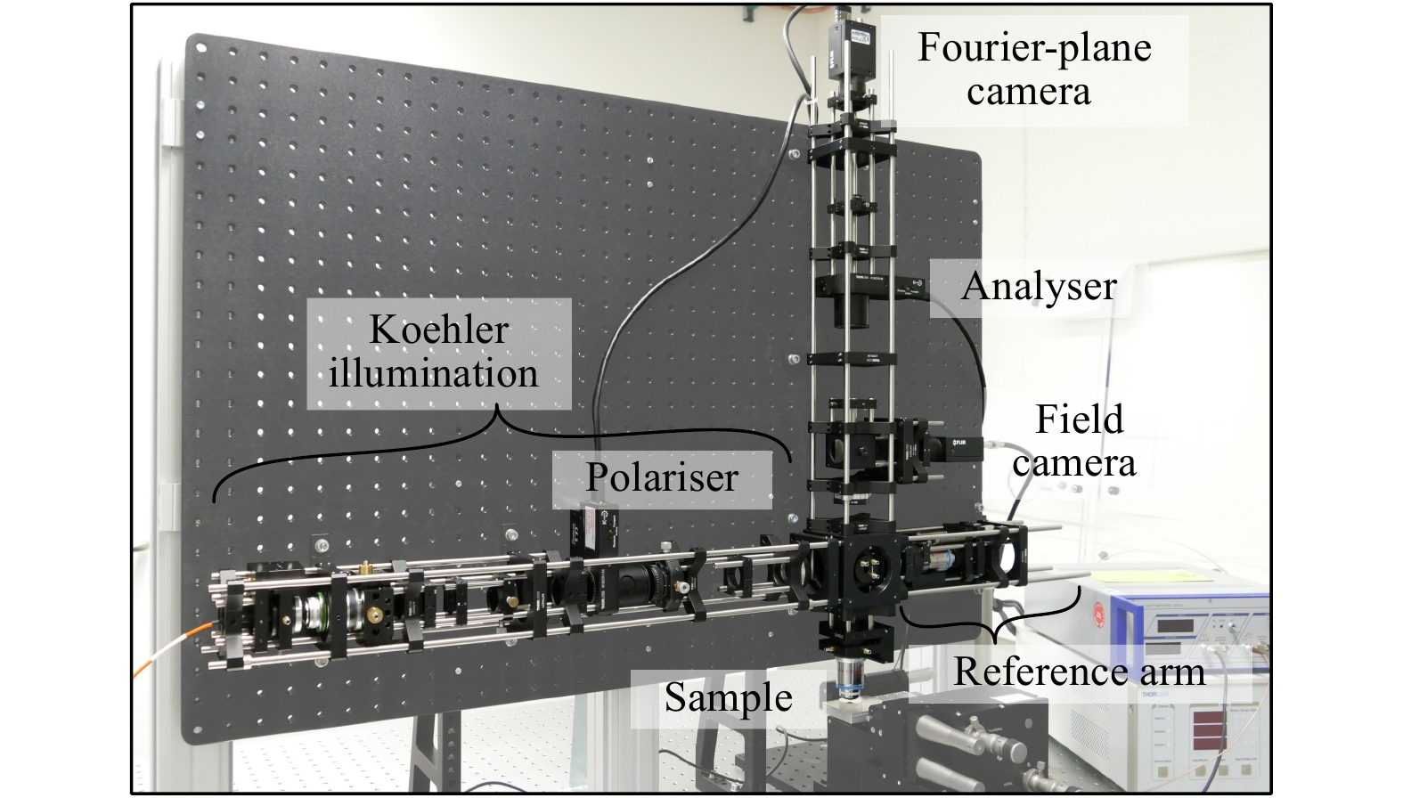
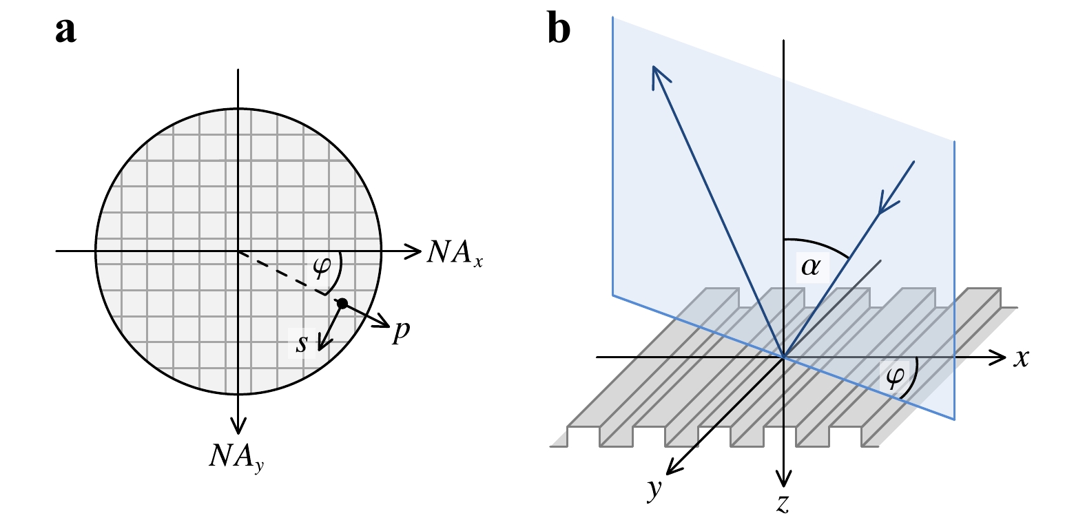
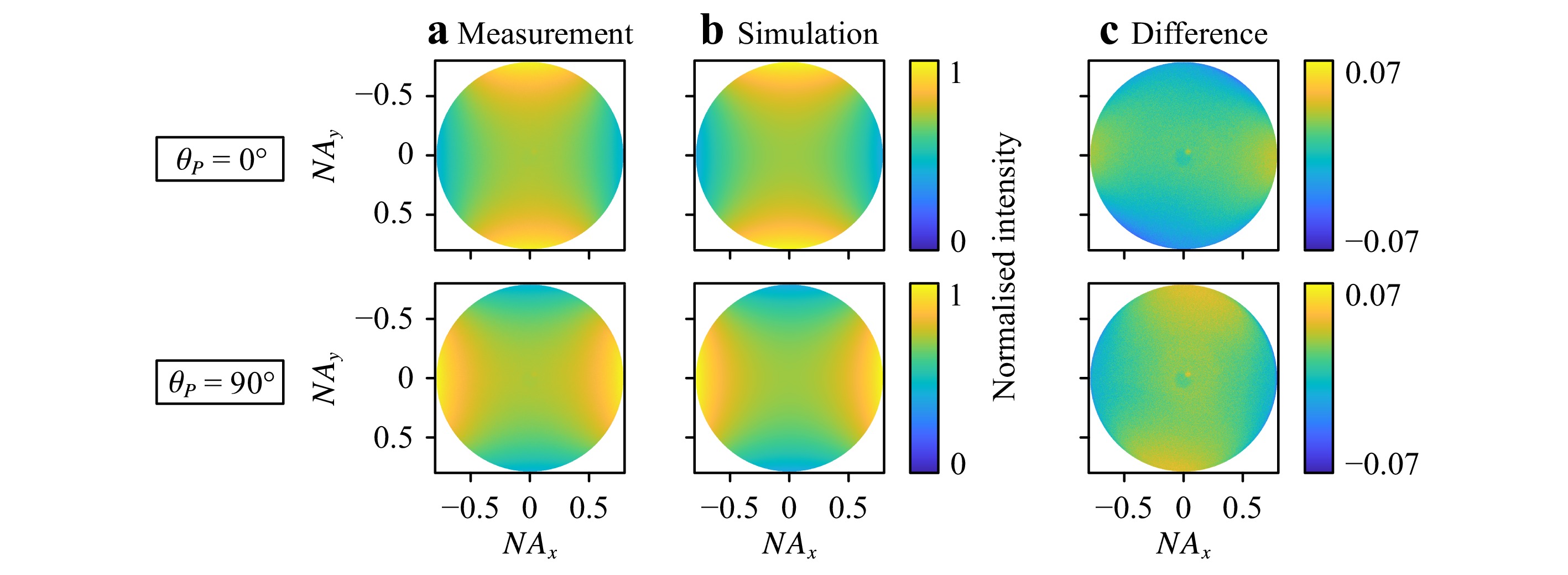
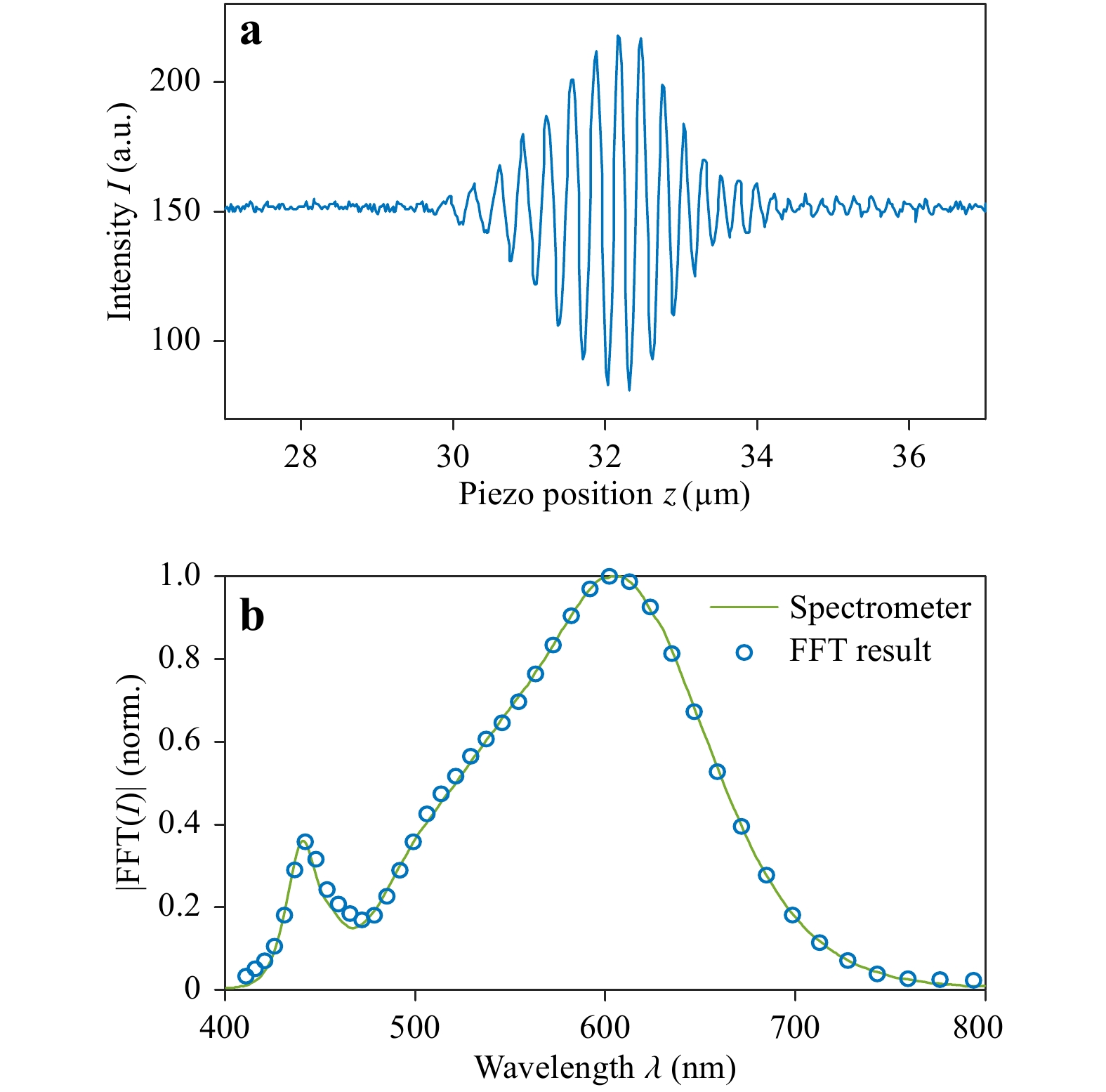
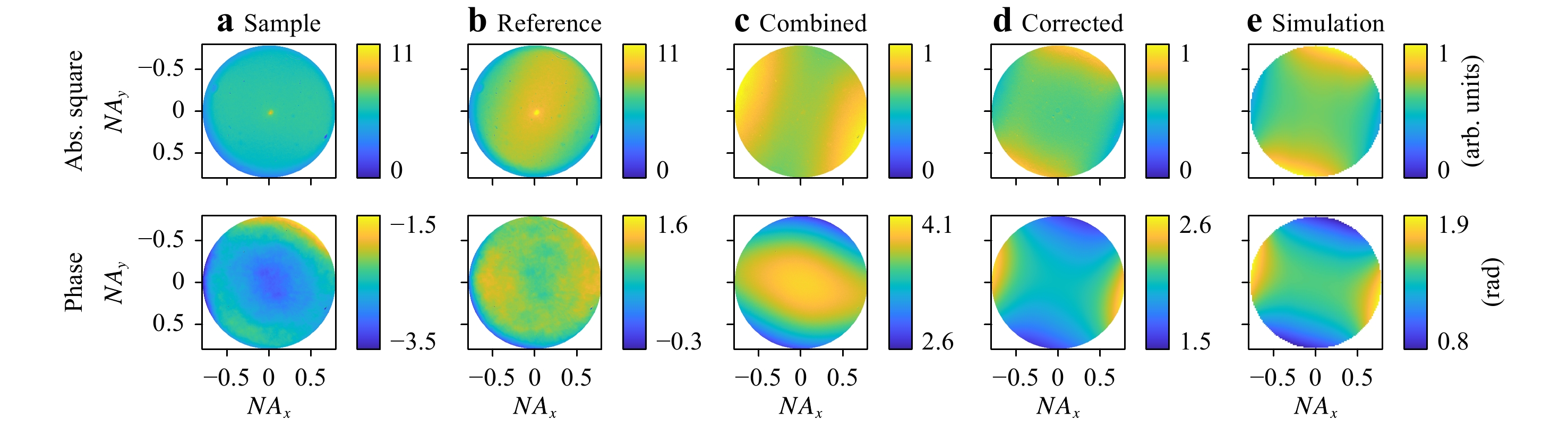
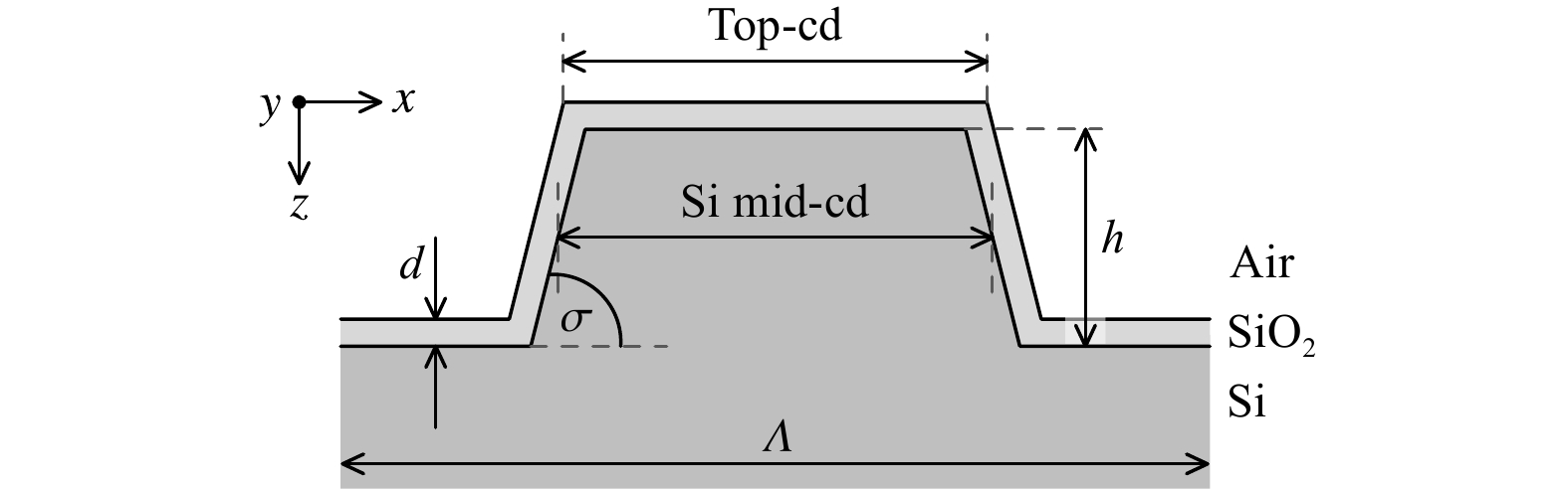
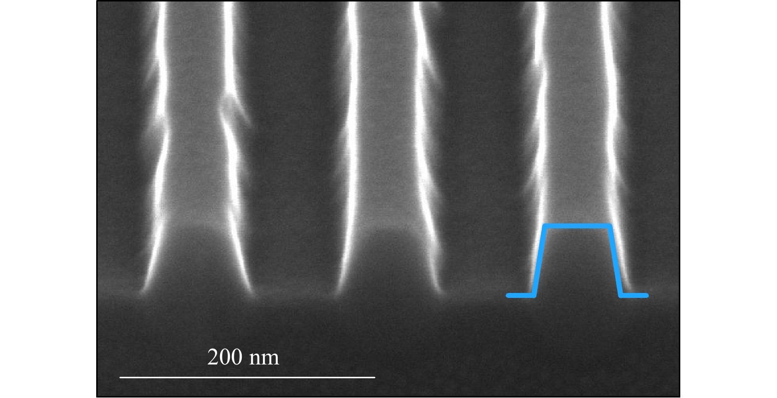
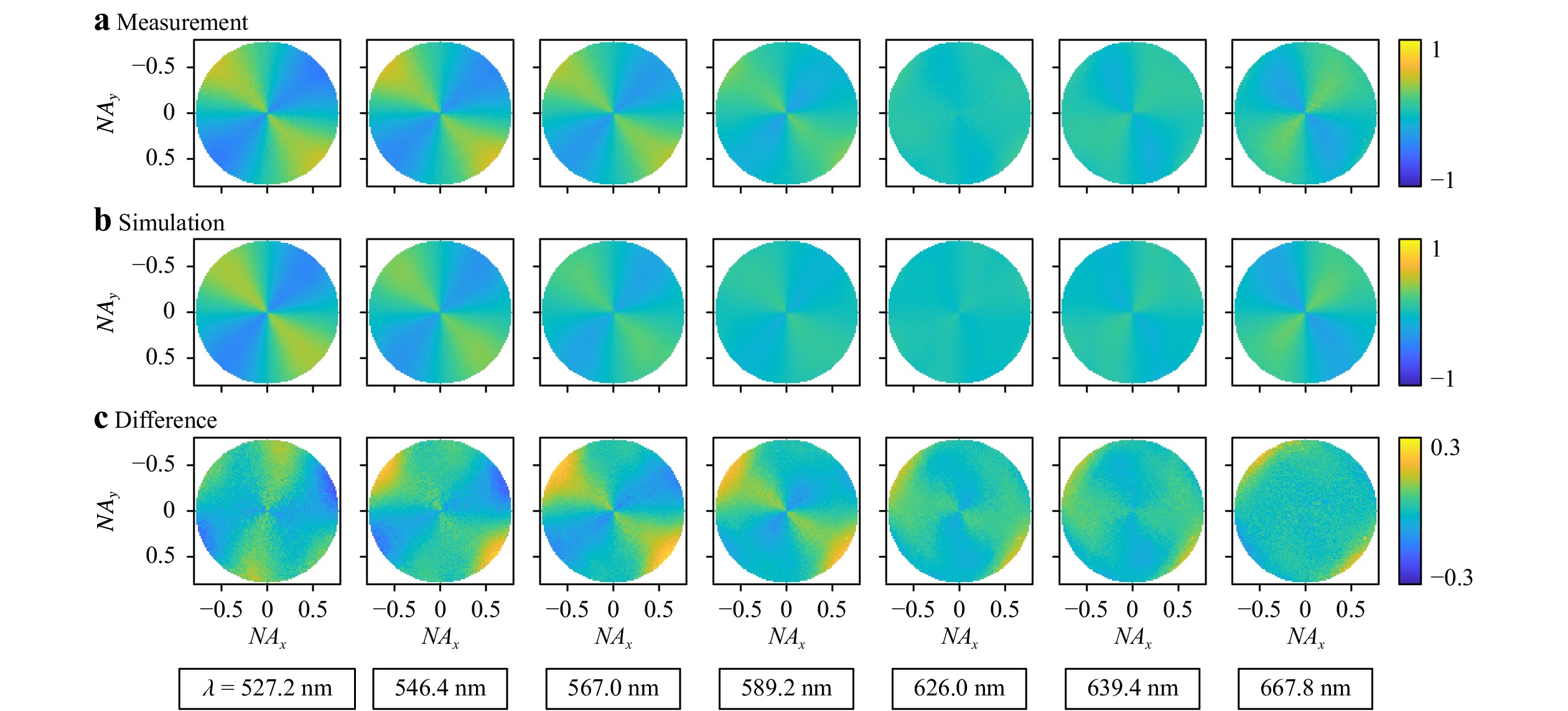
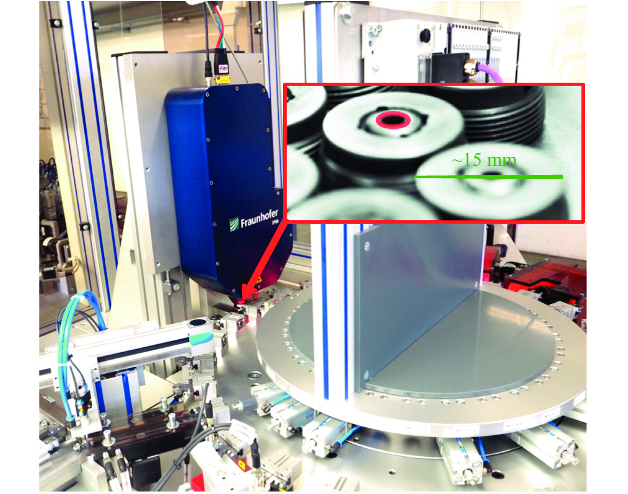
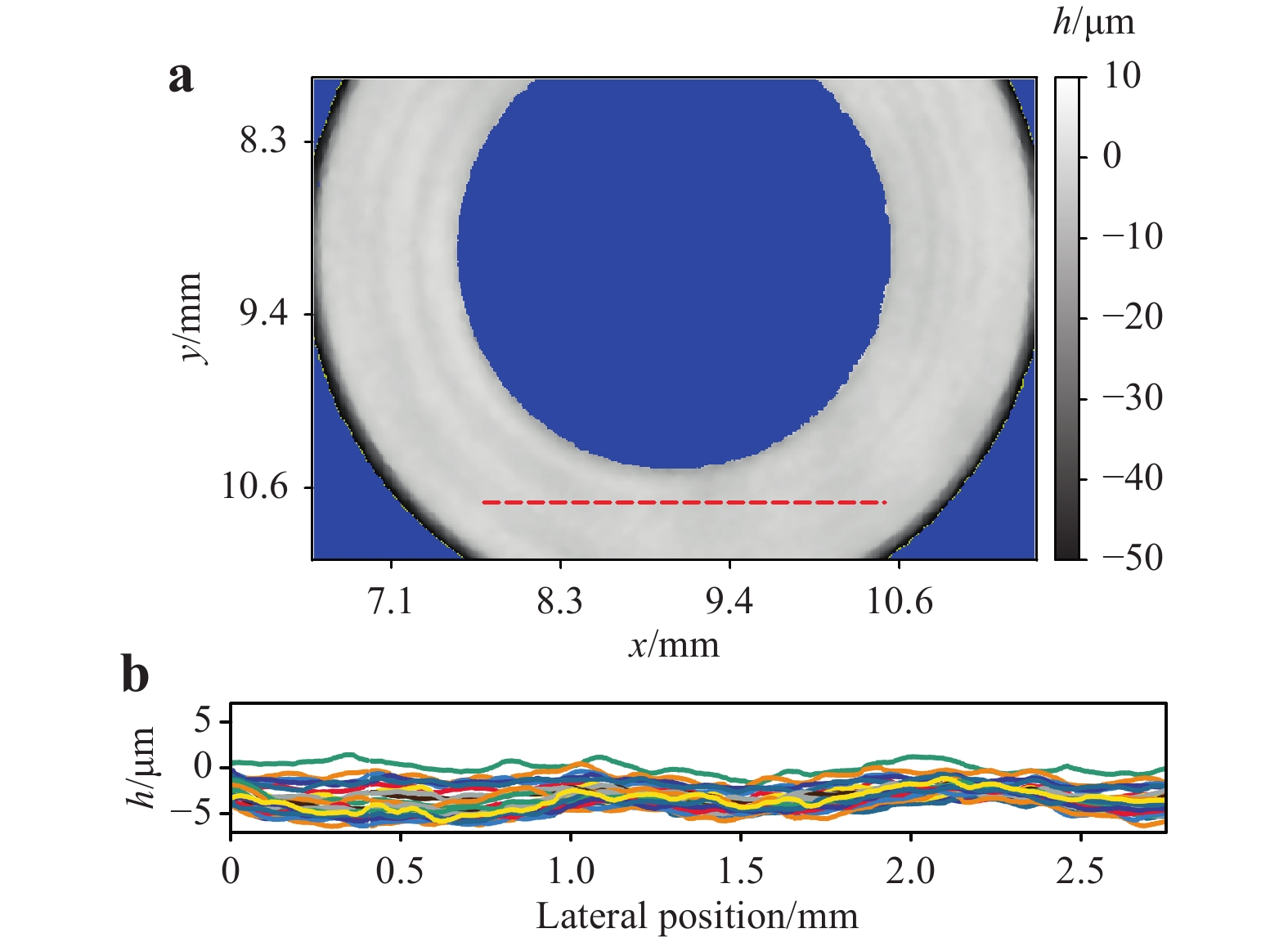
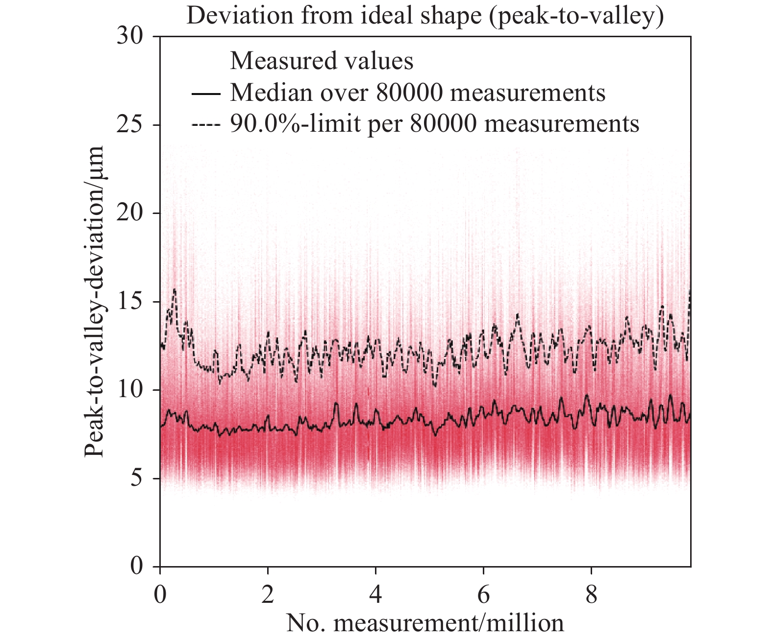
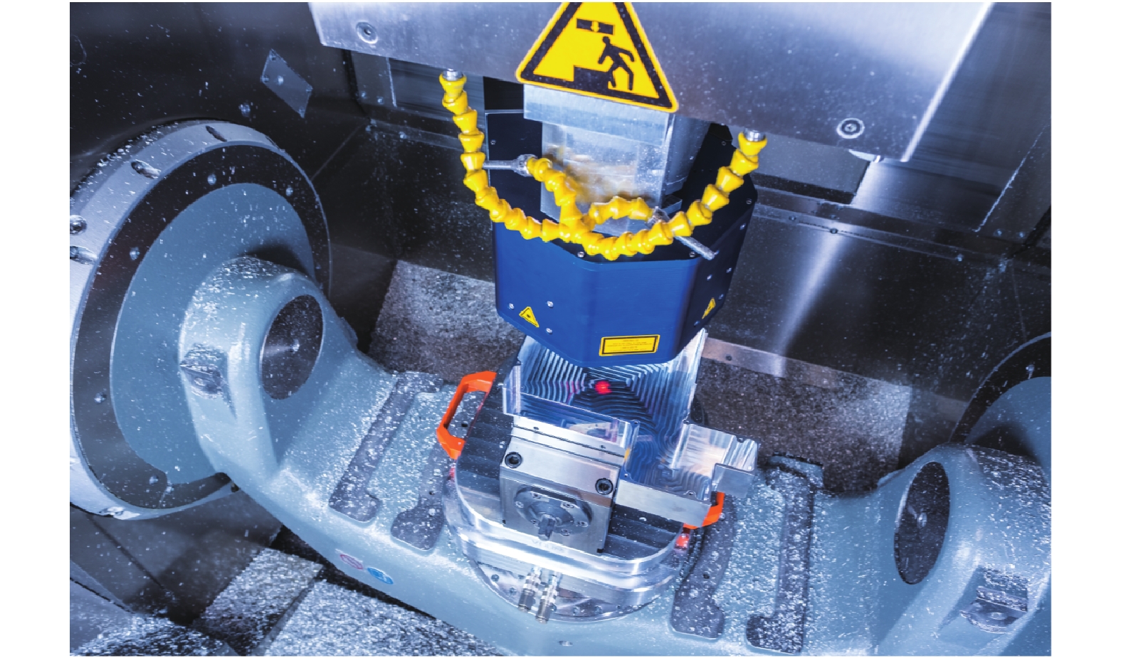
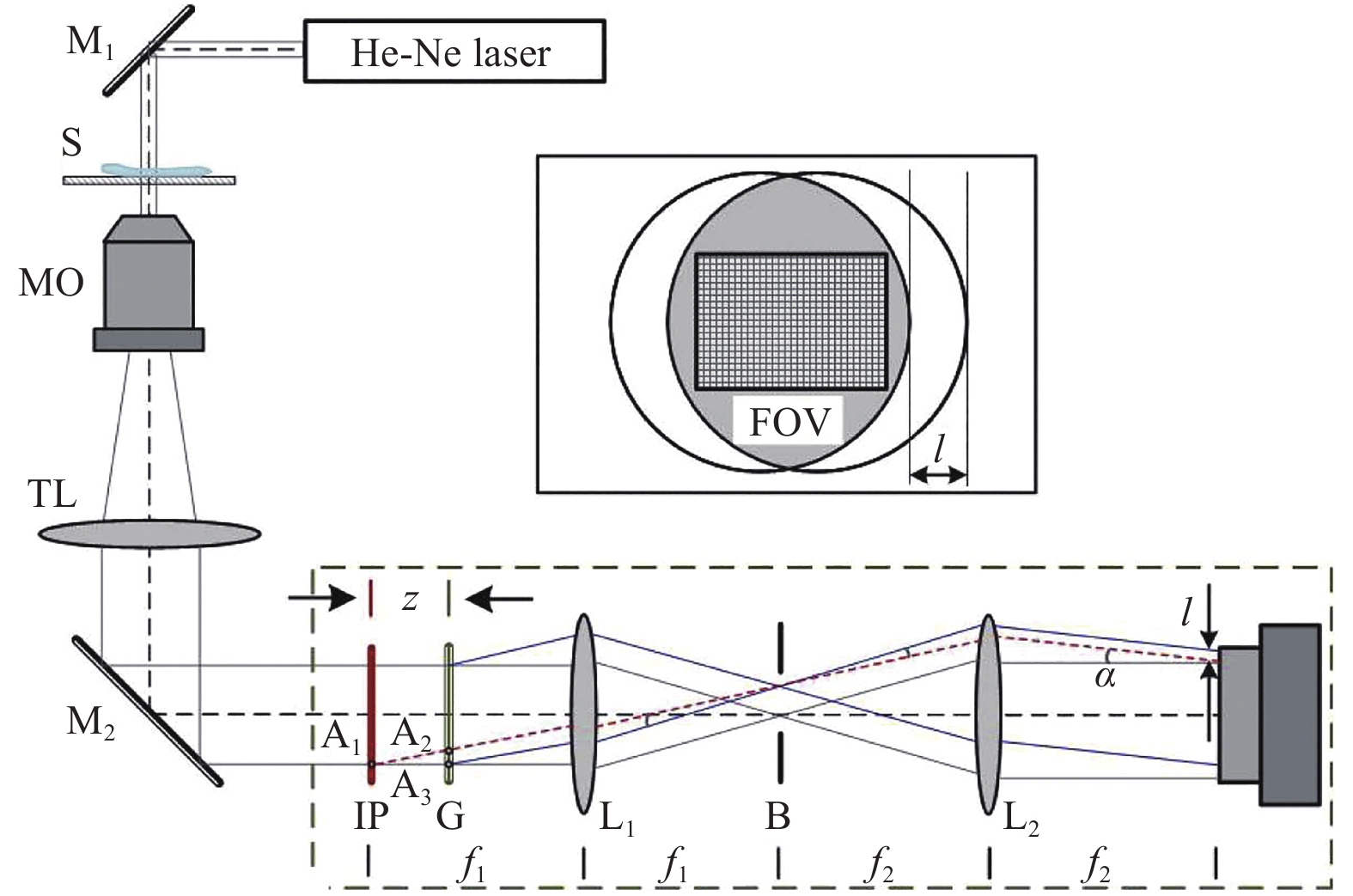
Optical scatterometry is one of the most important metrology techniques for process monitoring in high-volume semiconductor manufacturing. By comparing measured signatures to modelled ones, scatterometry indirectly retrieves the dimensions of nanostructures and, hence, solves an inverse problem. However, the increasing design complexity of modern semiconductor devices makes modelling of the structures ever more difficult and requires a multitude of parameters. Such large parameter spaces typically cause ambiguities in the reconstruction process, thereby complicating the solution of the inherently ill-posed inverse problem further. An effective means of regularisation consists of systematically maximising the information content provided by the optical sensor. With this in mind, we combined the classical techniques of white-light interferometry, Mueller polarimetry, and Fourier scatterometry into one apparatus, allowing for the acquisition of fully angle- and wavelength-resolved Mueller matrices. The large amount of uncorrelated measurement data improve the robustness of the reconstruction in the case of complex multi-parameter problems by increasing the overall sensitivity and reducing cross-correlations. In this study, we discuss the sensor concept and introduce the measurement strategy, calibration routine, and numerical post-processing steps. We verify the practical feasibility of our method by reconstructing the profile parameters of a sub-wavelength silicon line grating. All necessary simulations are based on the rigorous coupled-wave analysis method. Additional measurements performed using a scanning electron microscope and an atomic force microscope confirm the accuracy of the reconstruction results, and hence, the real-world applicability of the proposed sensor concept.

Active tuning of electromagnetically induced transparency from chalcogenide-only metasurface
Kuan Liu, Meng Lian, Kairong Qin, Shuang Zhang, Tun Cao
Published. 2021, 2(3) : 251-261 doi: 10.37188/lam.2021.019

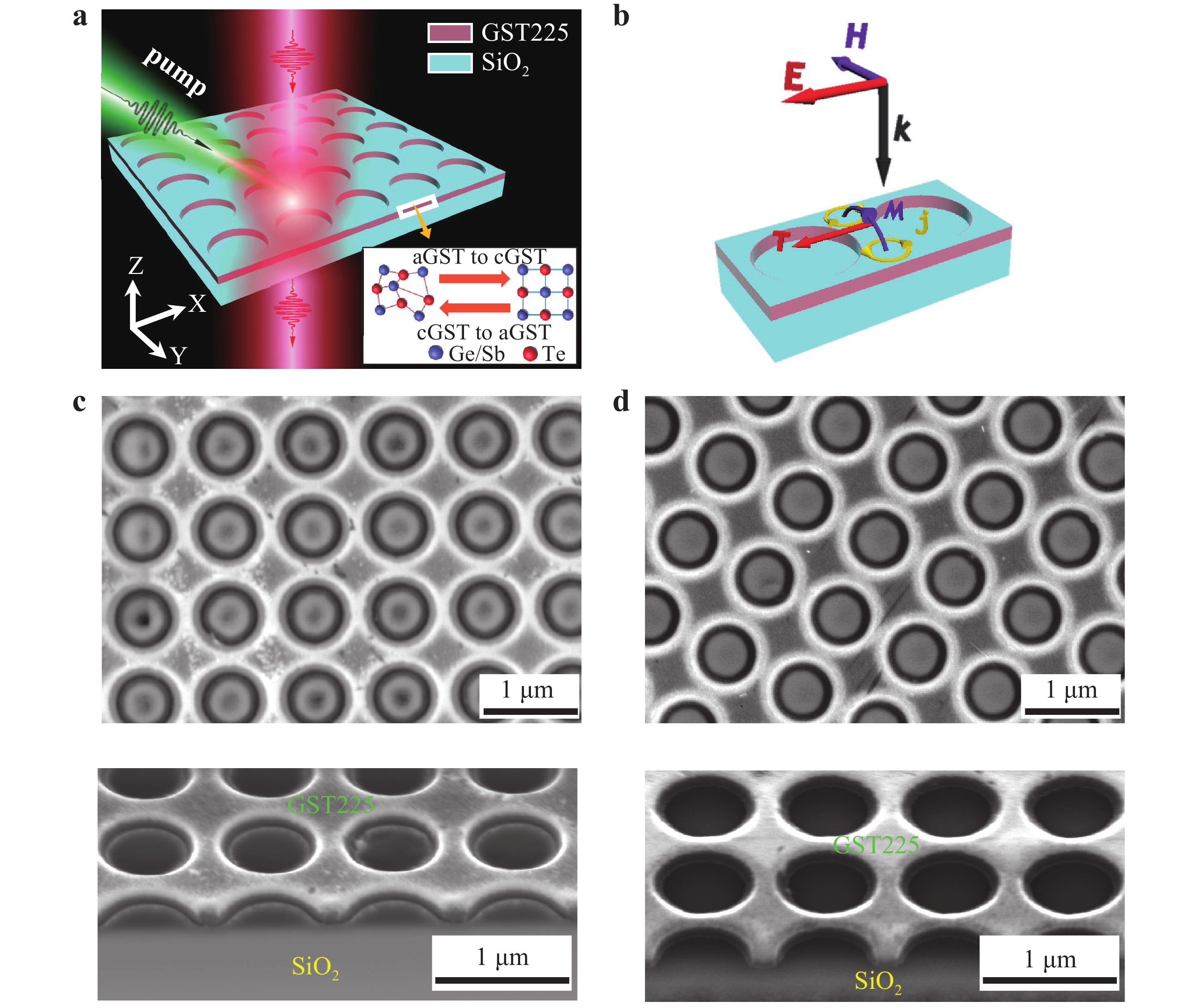
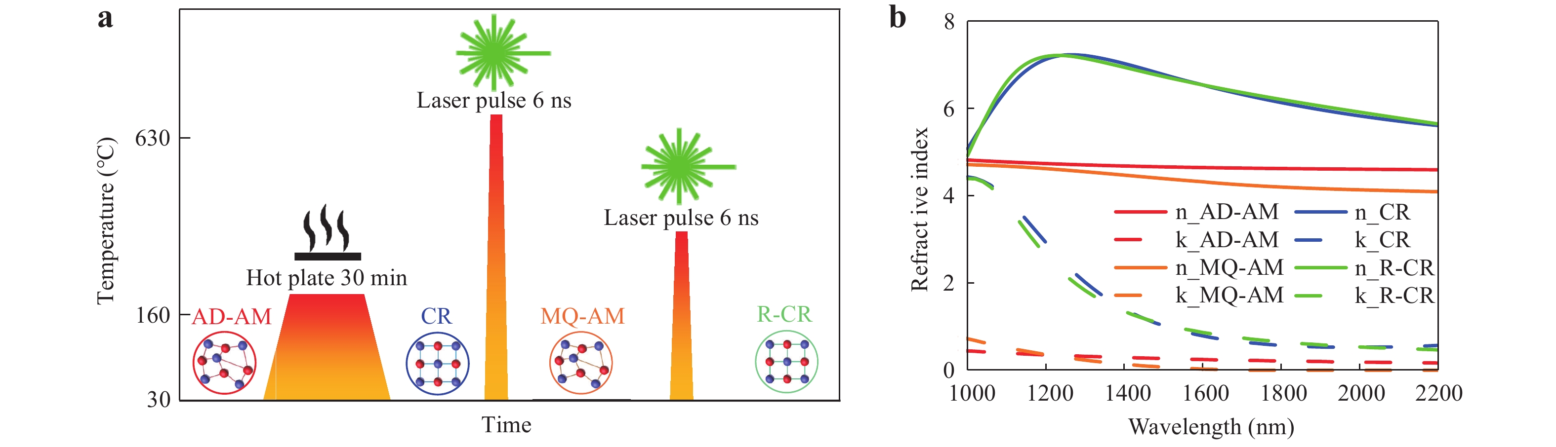
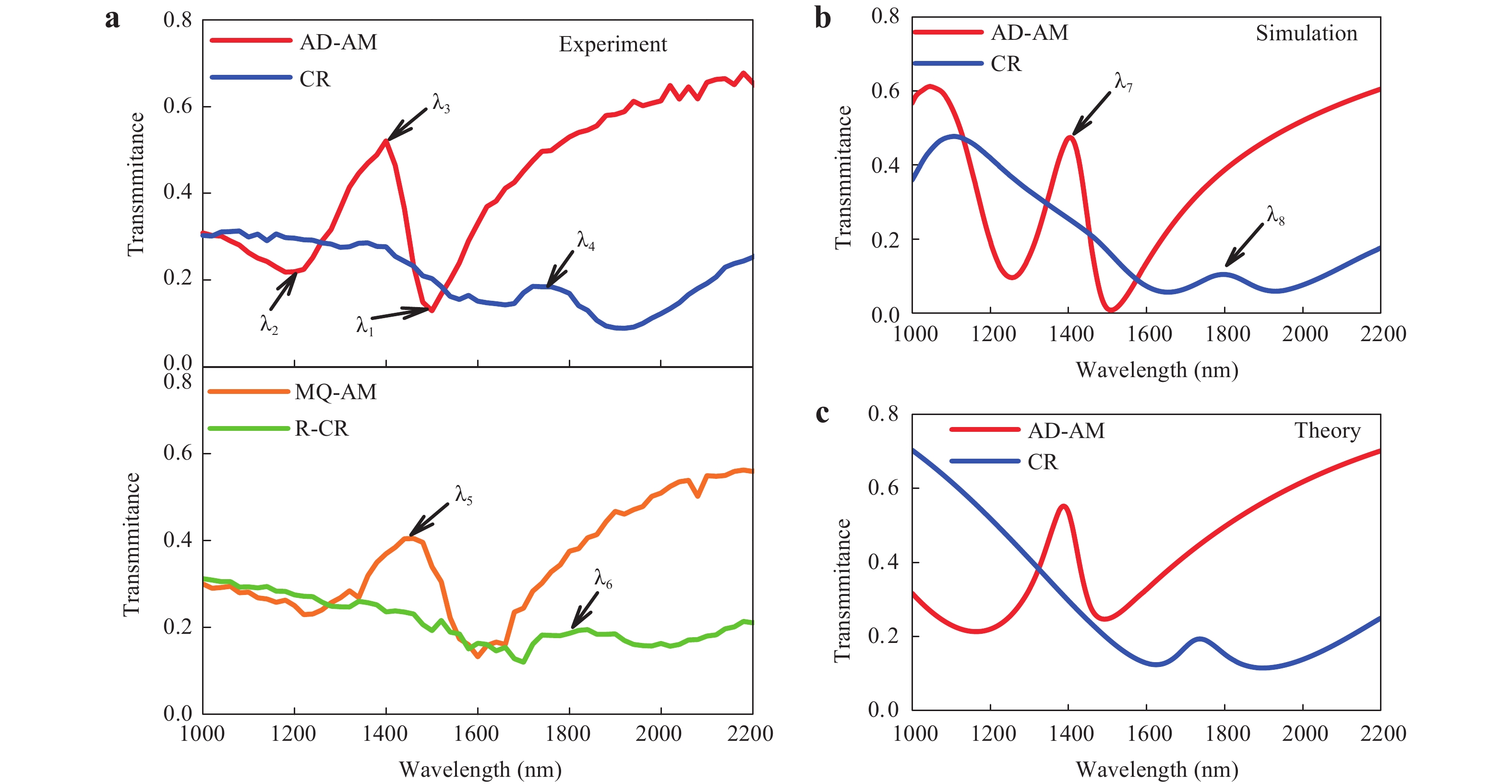
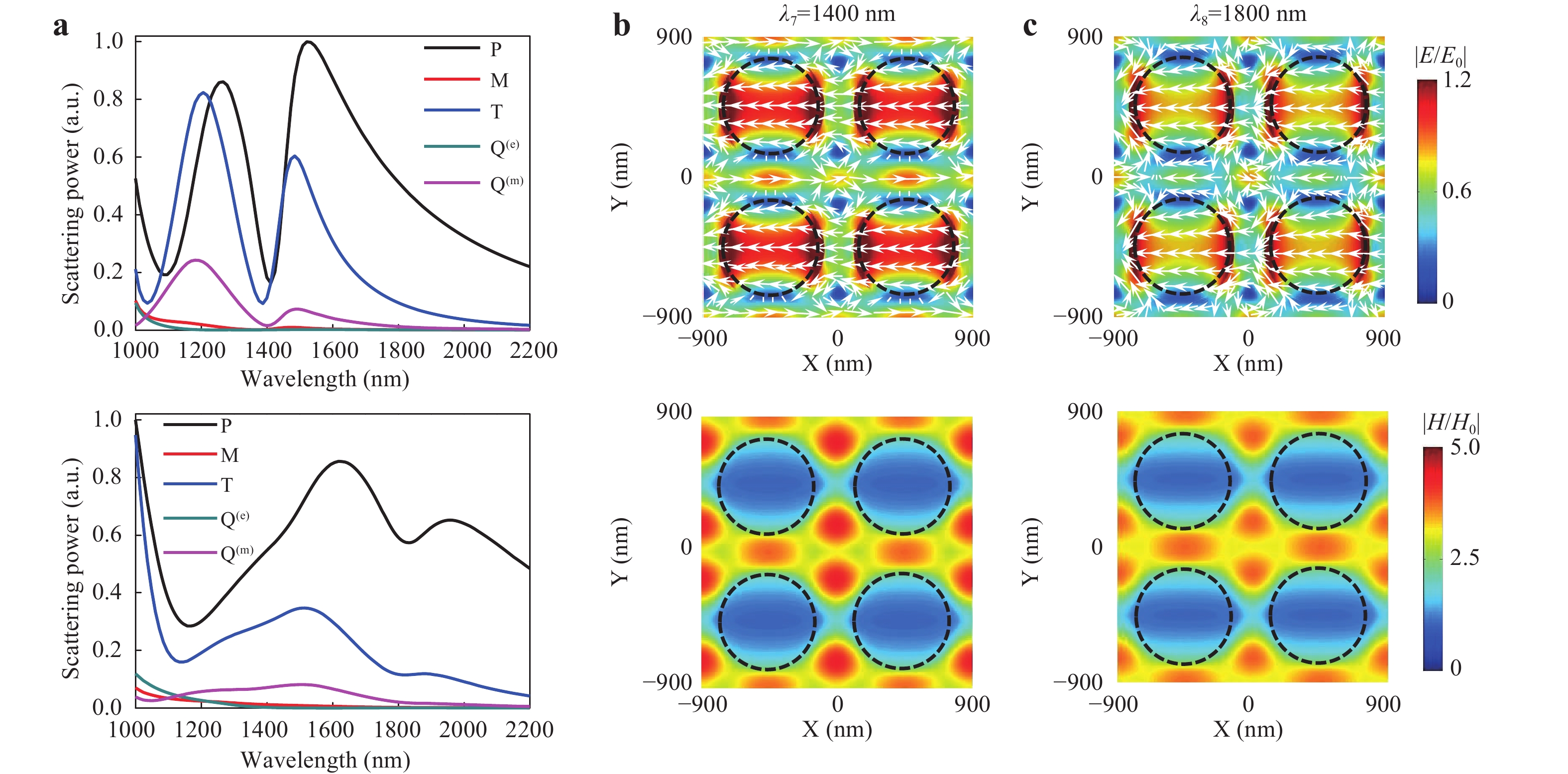
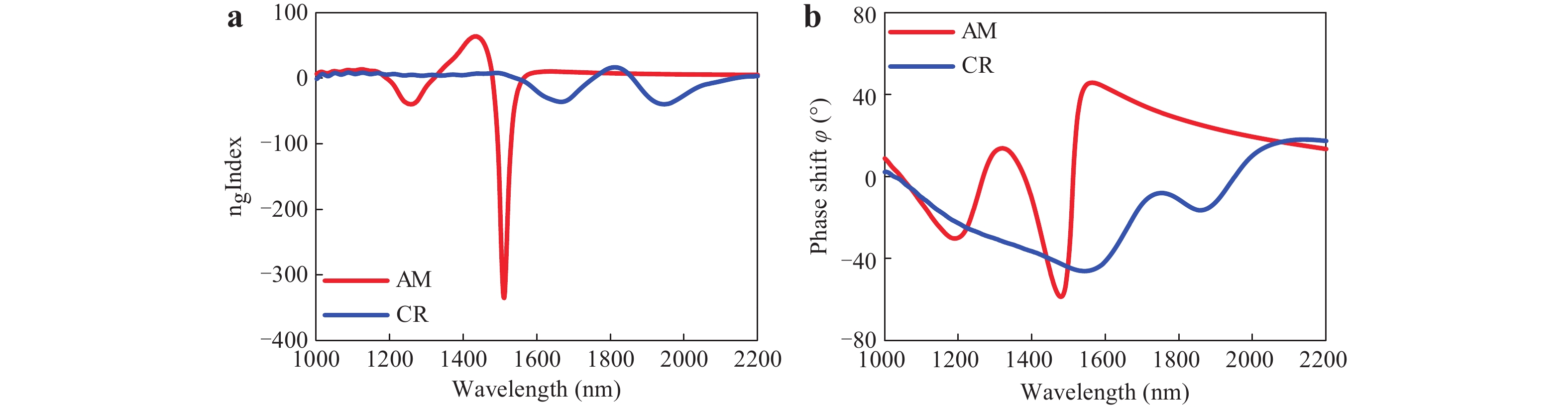
Electromagnetically induced transparency (EIT) is a coherent optical process that provides a narrow transparent peak within a broad absorption line in an atomic medium. All-dielectric metasurface analogues of EIT have enabled new developments in the nanophotonics field for obtaining smaller, more effective slow-light devices and highly sensitive detectors without a quantum approach. However, the dynamic control of the EIT response of all-dielectric metasurfaces has been rarely reported hitherto for the near-infrared (N-IR) region, although a broader range of applications will be enabled by a reconfigurable EIT system. In this study, we realise a chalcogenide (germanium antimony telluride, GST) metasurface, which possesses a dynamically tunable EIT response by optically driving the amorphous-crystalline phase change in the GST medium. Only a few tens of nanometres thick, the nanostructured GST film exhibits Mie resonances that are spectrally modified via laser-induced phase transitions, offering a high relative modulation contrast of 80% in the N-IR region. Moreover, an extreme dispersion that results in the ‘slow light’ behaviour is observed within this transparency ‘window’. Furthermore, the group delay of the N-IR beam switches reversibly under the phase transition. The measurement is consistent with both numerical simulation results and phenomenological modelling. Our work facilitates the development of new types of compact ultrafast N-IR holograms, filtering, and ultrasensitive detectors.

Longitudinally thickness-controlled nanofilms on exposed core fibres enabling spectrally flattened supercontinuum generation
Tilman A. K. Lühder, Henrik Schneidewind, Erik P. Schartner, Heike Ebendorff-Heidepriem, Markus A. Schmidt
Published. 2021, 2(3) : 262-273 doi: 10.37188/lam.2021.021
Nonlinear frequency conversion is a pathway to unlock undiscovered physics and implement tailored light sources for spectroscopy or medicine. A key challenge is the establishment of spectrally flat outputs, which is particularly demanding in the context of soliton-based light conversion at low pump energy. Here, we introduce the concept of controlling nonlinear frequency conversion by longitudinally varying resonances, allowing the shaping of soliton dynamics and achieving broadband spectra with substantial spectral flatness. Longitudinally varying resonances are realised by nanofilms with gradually changing thicknesses located on the core of an advanced microstructured fibre. Nanofilms with engineered thickness profiles are fabricated by tilted deposition, representing a waveguide-compatible approach to nano-fabrication, and inducing well-controlled resonances into the system, allowing unique dispersion control along the fibre length. Key features and dependencies are examined experimentally, showing improved bandwidth and spectral flatness via multiple dispersive wave generation and dispersion-assisted soliton Raman shifts while maintaining excellent pulse-to-pulse stability and coherence in simulations, suggesting the relevance of our findings for basic science as well as tailored light sources.
Controllable generation of large-scale highly regular gratings on Si films
Jiao Geng, Xiaoguo Fang, Lei Zhang, Guangnan Yao, Liye Xu, et al.
Published. 2021, 2(3) : 274-282 doi: 10.37188/lam.2021.022
The application of femtosecond laser-induced periodic surface texturing has significant potential in medicine, optics, tribology, and biology, among other areas. However, when irradiated by a large intense laser spot, the periodic structures usually exhibit an uncontrollable regularity, forming bifurcated patterns, thus limiting their widespread application. Irregularity originates from numerous independent branching seeds. The usual solution to this problem is to utilize the quasi-direct laser writing technique, that is, by limiting the laser beam size (diameter of <10 wavelengths) and scanning the beam or samples using 2D translation stages. Herein, we demonstrate an optical localization-induced nonlinear competition mechanism to solve this problem, which occurs at a fluence nearly one order of magnitude below the ablation threshold. Owing to the low intrinsic absorption of silicon and ultralow applied fluence, this mechanism ensures the self-selection of a single seed to initiate an array of bifurcated-free gratings under stationary irradiation with a large laser spot (diameter >100 wavelengths). Surprisingly, some unconventional complex patterns, such as radial, annular, and spiral gratings, can also be easily produced by structured light fields with unprecedented regularity. Their diameters reach up to >500 μm. Moreover, we can artificially control the initial seeding structure to further improve the regularity of the gratings, defined by dispersion in the ripple orientation angle in their 2D Fourier transform. As a result, the regularity in our experiments produced by a large laser spot is even higher than that scanned by a tiny beam. Controllable and highly regular ripples are beneficial to the structural coloring effects because they arise from the light diffraction by subwavelength gratings.
Review
Digital holography in production: an overview
Markus Fratz, Tobias Seyler, Alexander Bertz, Daniel Carl
Published. 2021, 2(3) : 283-295 doi: 10.37188/lam.2021.015
Many challenging measurement tasks in production simultaneously have high requirements for accuracy, measurement field size, lateral sampling, and measurement time. In this paper, we provide an overview of the current state of the art in digital holography for surface topography measurements and present three applications from completely different productions with no alternative to digital holography; we describe the HoloTop sensor family, which has been designed specifically for industrial use, and present the most recent results achieved in real-life industrial applications. All applications address measurement tasks that could not be solved until now, either by optical or tactile means. We start with a description of the first-ever inline integration of a digital holographic measurement system that inspects precision turned parts for the automotive industry. We proceed by presenting measurements performed with a compact sensor that can be placed inside a tooling machine and operated fully wirelessly. In this case, the tool holder was used to position the sensor directly. Integration into a tooling machine places high demands on both robustness and reliability. Finally, the quality control of electronic interconnectors such as microbumps with the highest demand for accuracy and repeatability is demonstrated. All of these applications illustrate the major advantages of digital holographic systems: it is possible to measure a relatively large field of view with interferometric precision and very short acquisition times. Additionally, both reflective and matt surfaces can be measured simultaneously. We end this publication with an assessment of the future potential of this technology and the necessary development steps involved.
Multi-material multi-photon 3D laser micro- and nanoprinting
Liang Yang, Frederik Mayer, Uwe H. F. Bunz, Eva Blasco, Martin Wegener
Published. 2021, 2(3) : 296-312 doi: 10.37188/lam.2021.017
Three-dimensional (3D) laser micro- and nanoprinting based upon multi-photon absorption has made its way from early scientific discovery to industrial manufacturing processes, e.g., for advanced microoptical components. However, so far, most realized 3D architectures are composed of only a single polymeric material. Here, we review 3D printing of multi-materials on the nano- and microscale. We start with material properties that have been realized, using multi-photon photoresists. Printed materials include bulk polymers, conductive polymers, metals, nanoporous polymers, silica glass, chalcogenide glasses, inorganic single crystals, natural polymers, stimuli-responsive materials, and polymer composites. Next, we review manual and automated processes achieving dissimilar material properties in a single 3D structure by sequentially photo-exposing multiple photoresists as 3D analogs of 2D multicolor printing. Instructive examples from biology, optics, mechanics, and electronics are discussed. An emerging approach – without counterpart in 2D graphical printing – prints 3D structures combining dissimilar material properties in one 3D structure by using only a single photoresist. A controlled stimulus applied during the 3D printing process defines and determines material properties on the voxel level. Change of laser power and/or wavelength, or application of quasi-static electric fields allow for the seamless manipulation of desired materials properties.
Review of laser powder bed fusion (LPBF) fabricated Ti-6Al-4V: process, post-process treatment, microstructure, and property
Sheng Cao, Yichao Zou, Chao Voon Samuel Lim, Xinhua Wu
Published. 2021, 2(3) : 313-332 doi: 10.37188/lam.2021.020

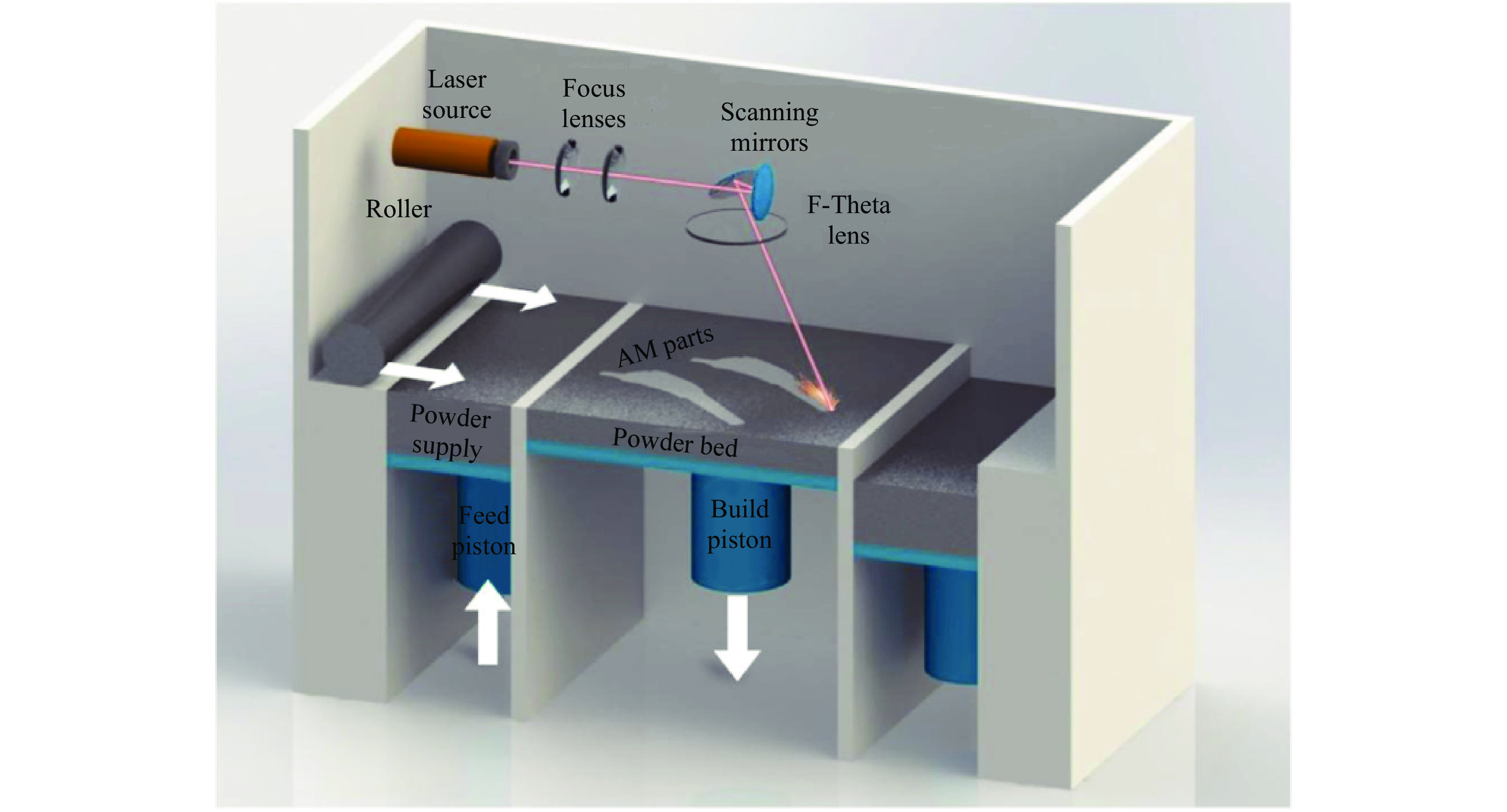
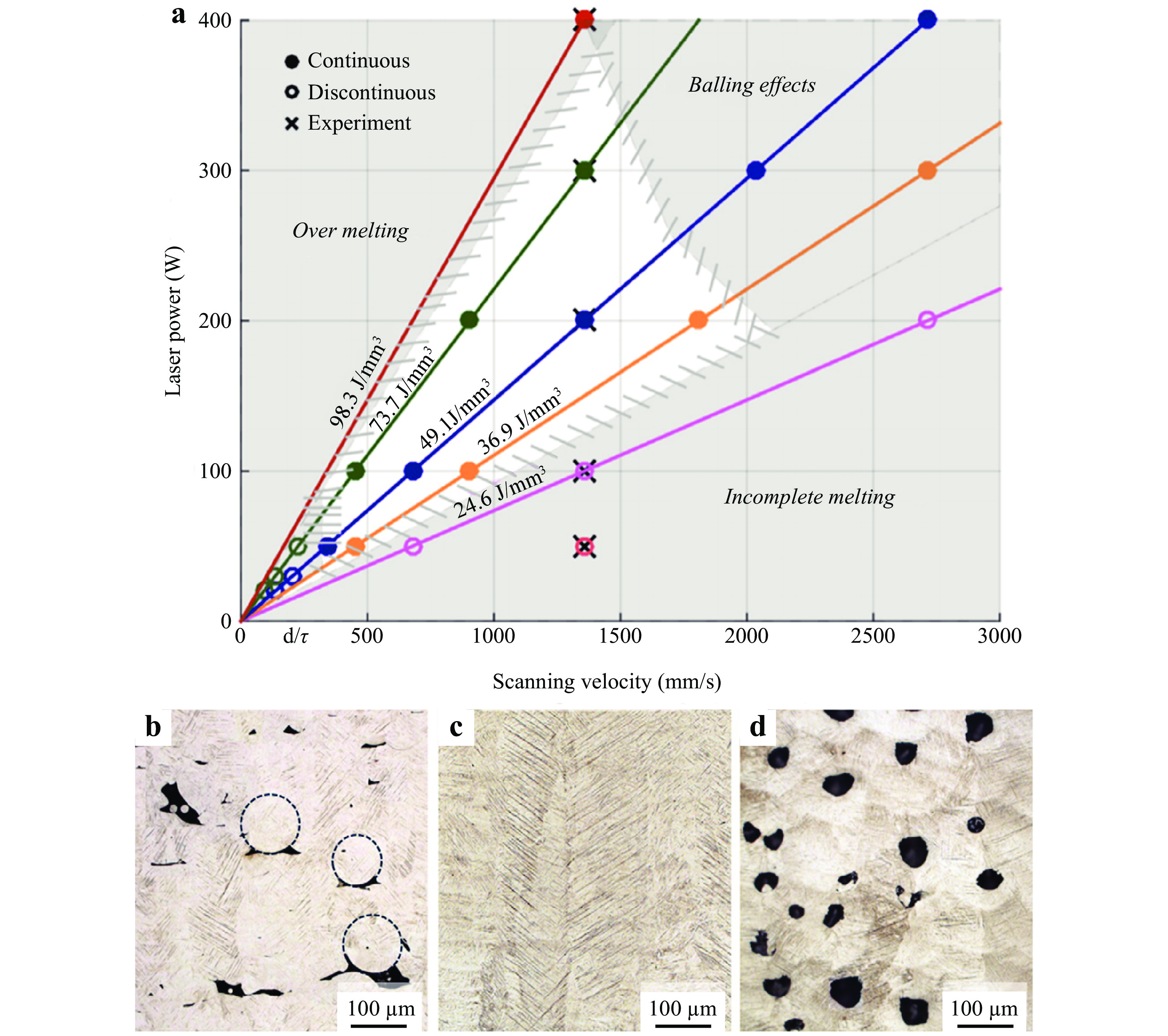
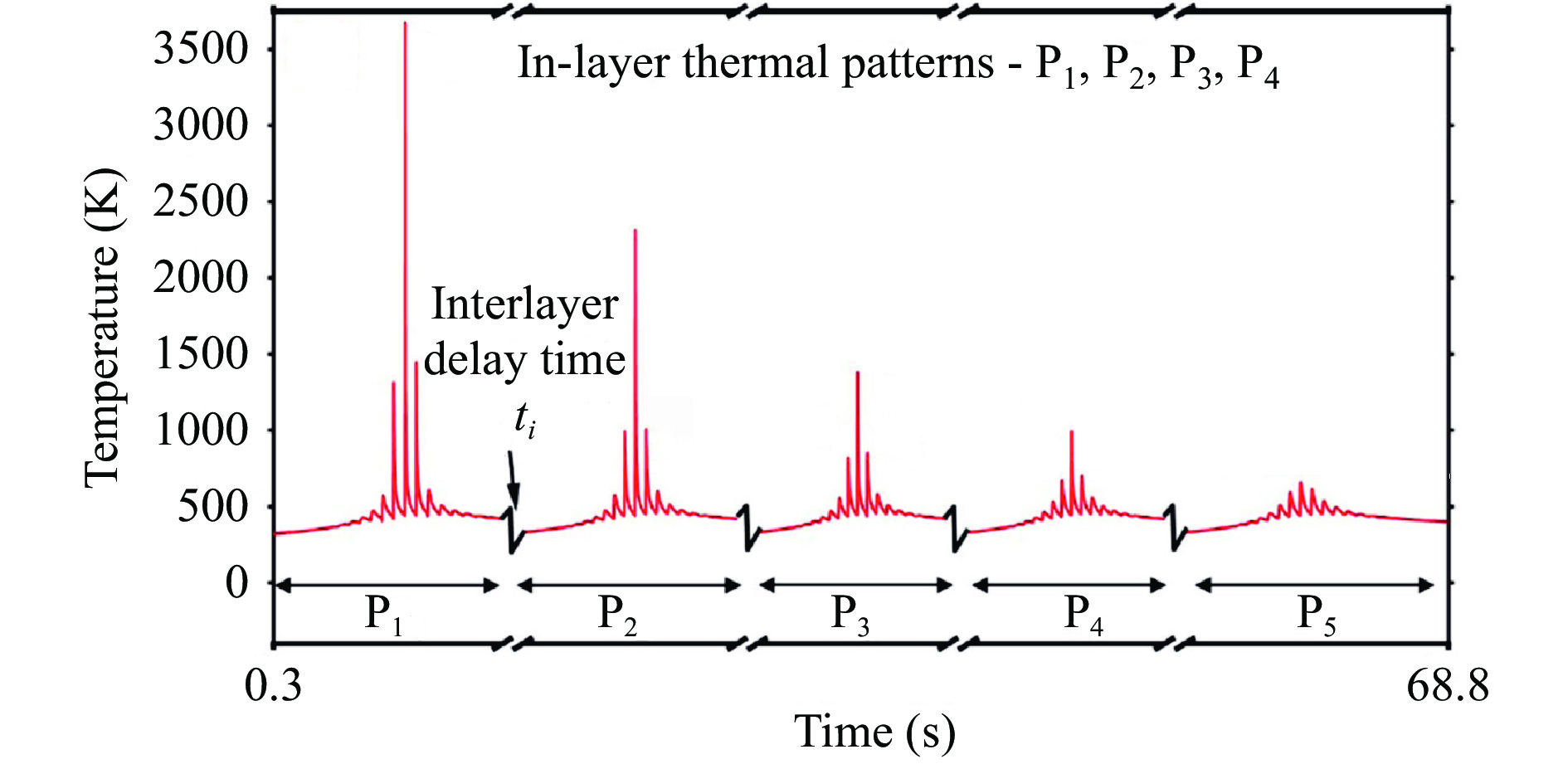
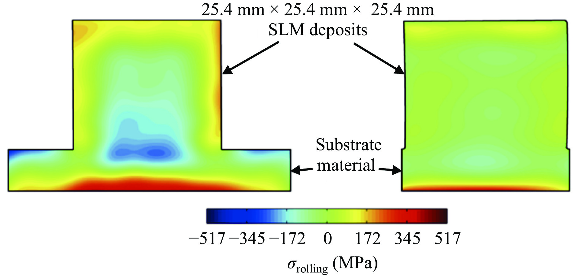
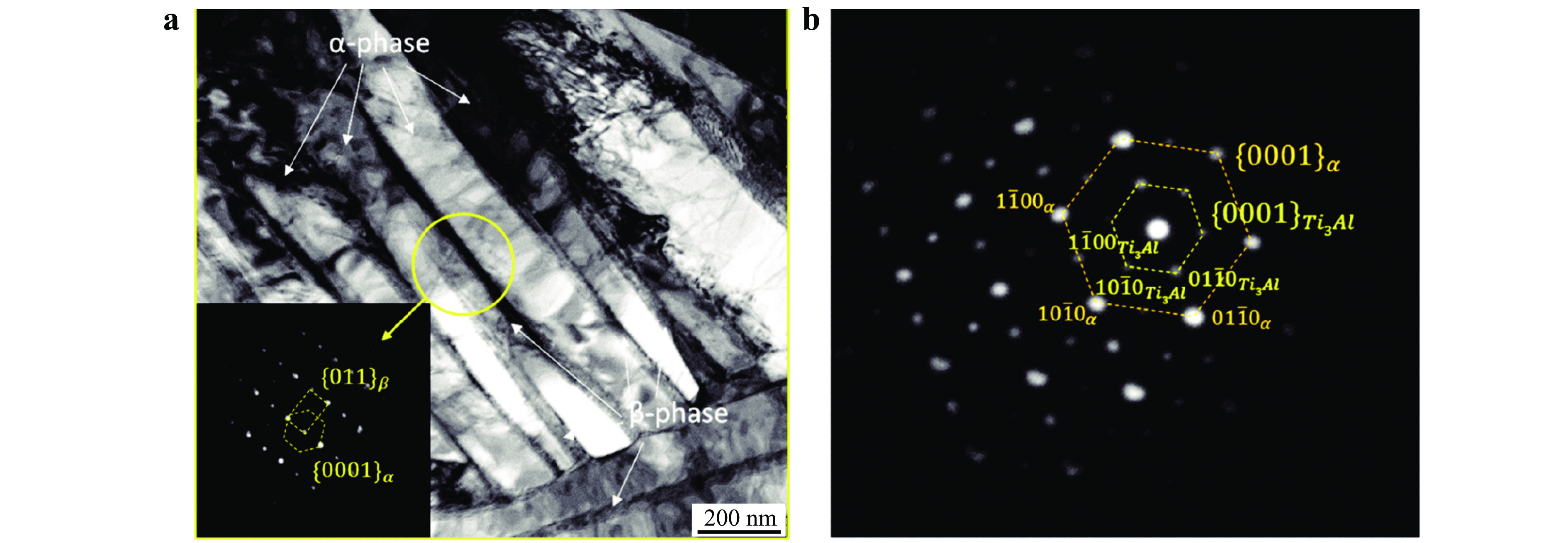
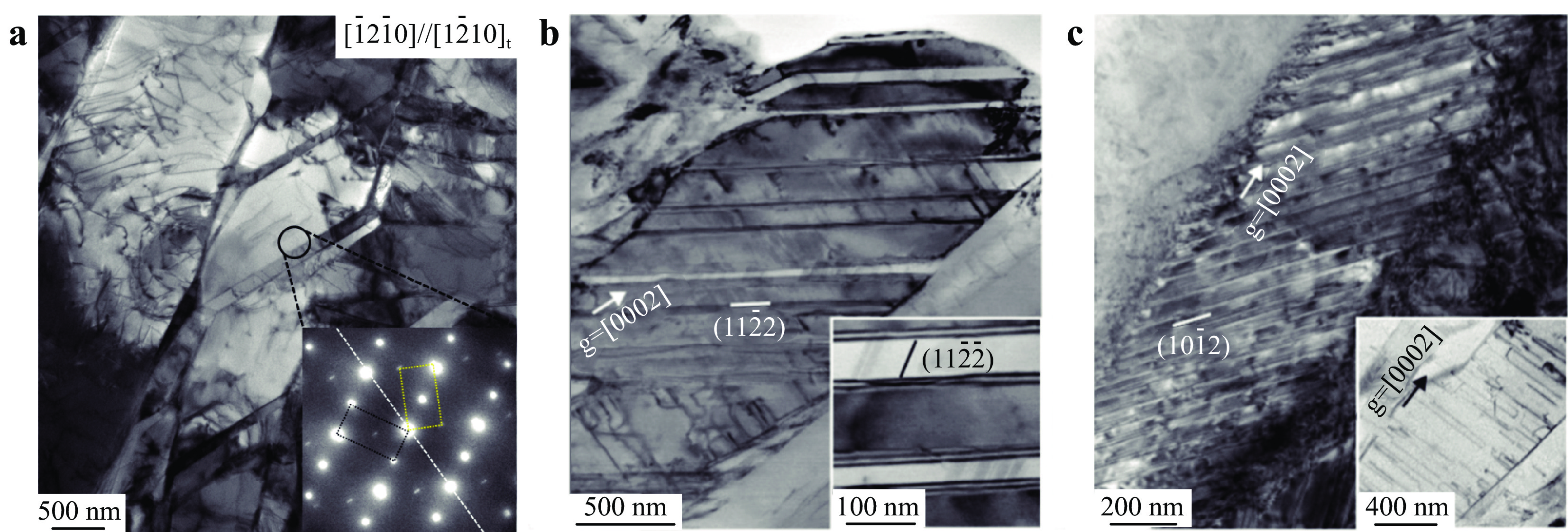
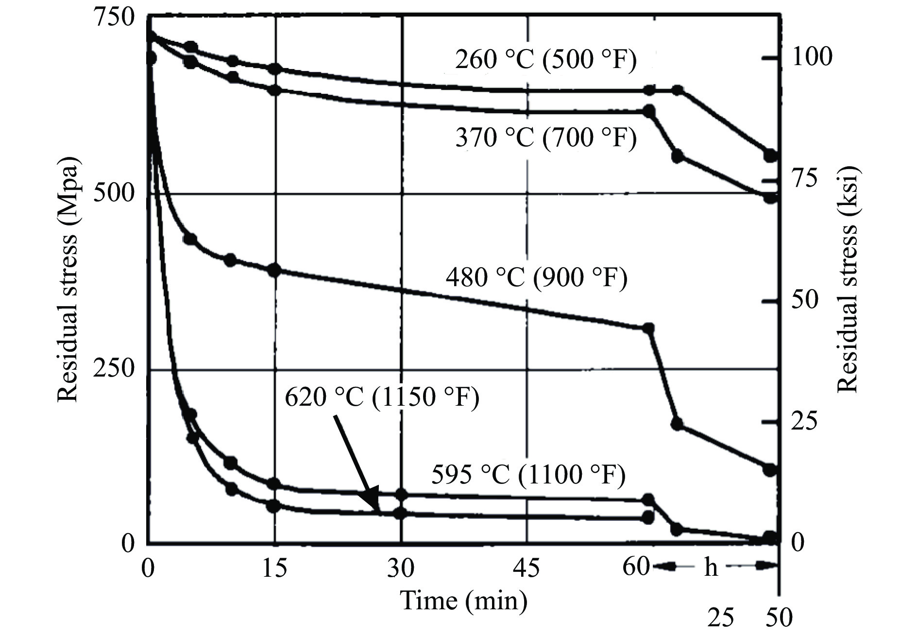
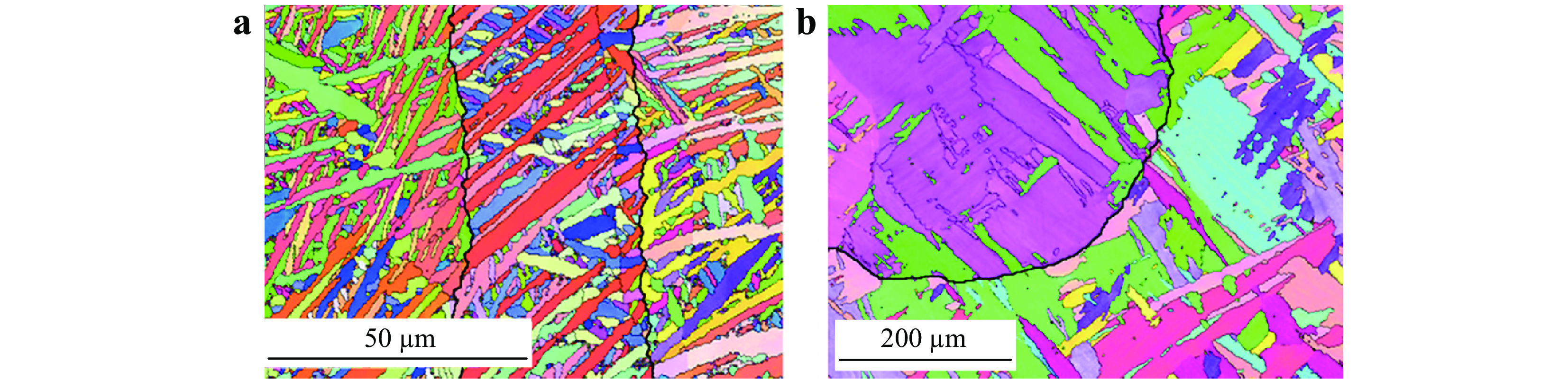
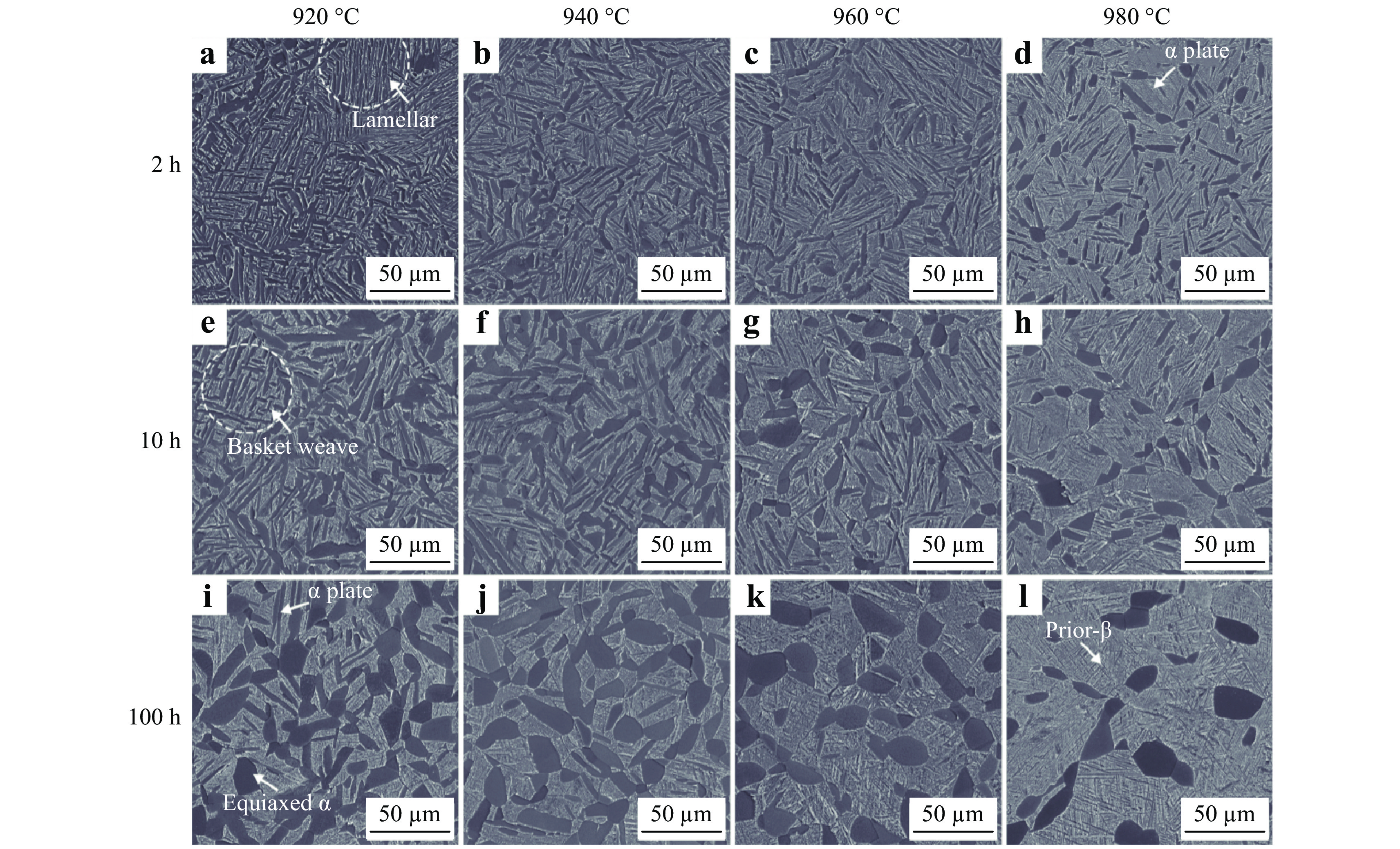
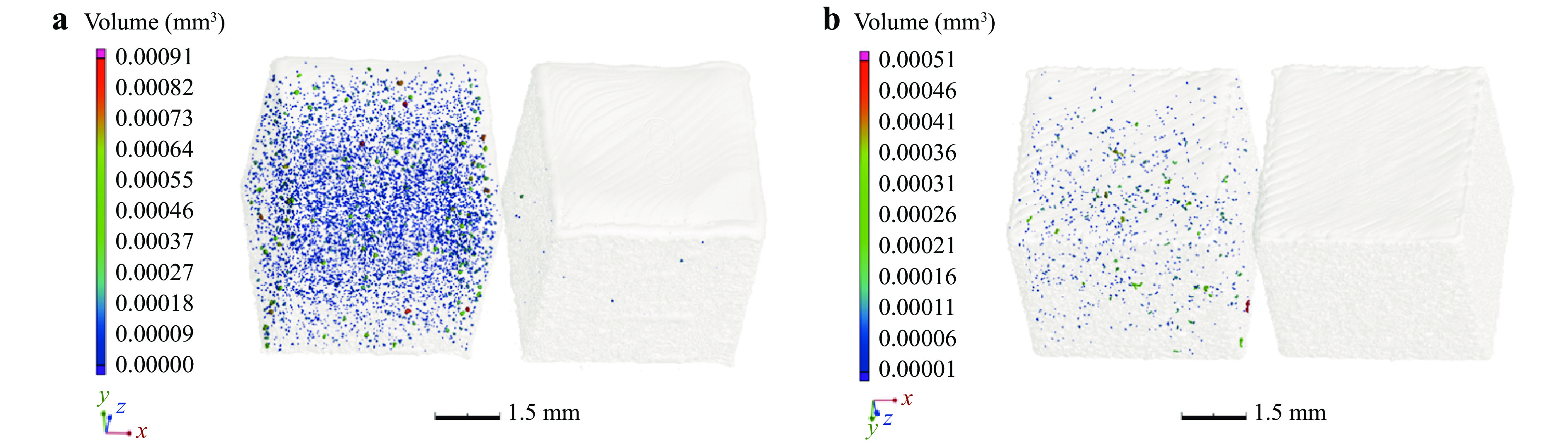
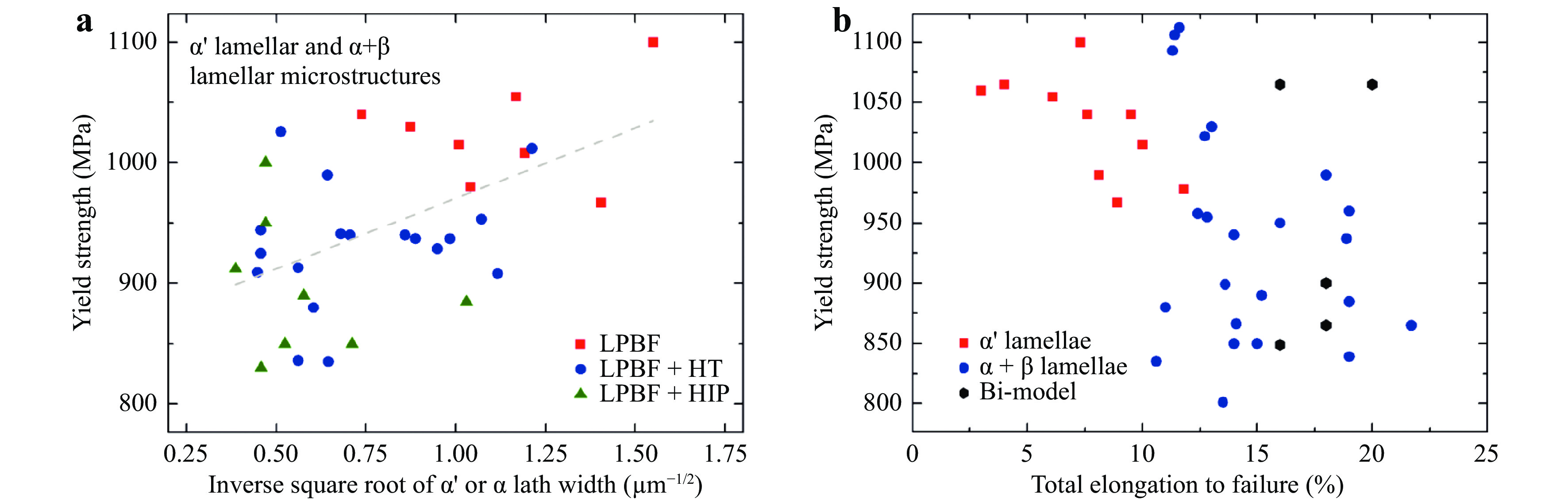
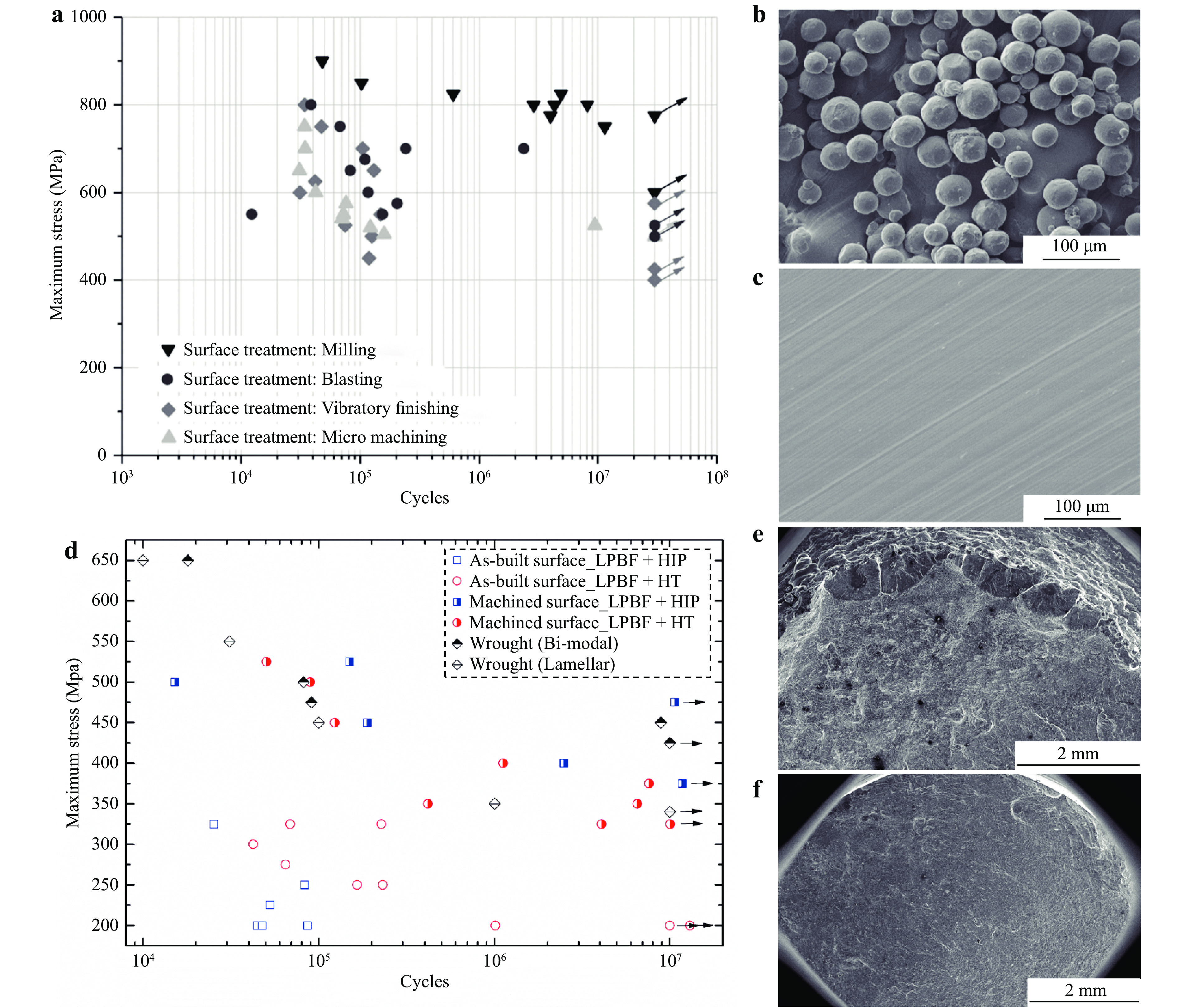
Laser powder bed fusion (LPBF) is a timely important additive manufacturing technique that offers many opportunities for fabricating three-dimensional complex shaped components at a high resolution with short lead times. This technique has been extensively employed in manufacturing Ti-6Al-4V parts for aerospace and biomedical applications. However, many challenges, including poor surface quality, porosity, anisotropy in microstructure and property, and difficulty in tailoring microstructure, still exist. In this paper, we review the recent progress in post-process treatment and its influence on the microstructure evolution and material performance, including tensile, fatigue, fracture toughness, creep, and corrosion properties. The contradictions in simultaneously achieving high strength/ductility and strength/fracture toughness/creep resistance have been identified. Furthermore, research gaps in understanding the effects of the emerging bi-modal microstructure on fatigue properties and fracture toughness require further investigation.

A review of common-path off-axis digital holography: towards high stable optical instrument manufacturing
Jiwei Zhang, Siqing Dai, Chaojie Ma, Teli Xi, Jianglei Di, et al.
Published. 2021, 2(3) : 333-349 doi: 10.37188/lam.2021.023

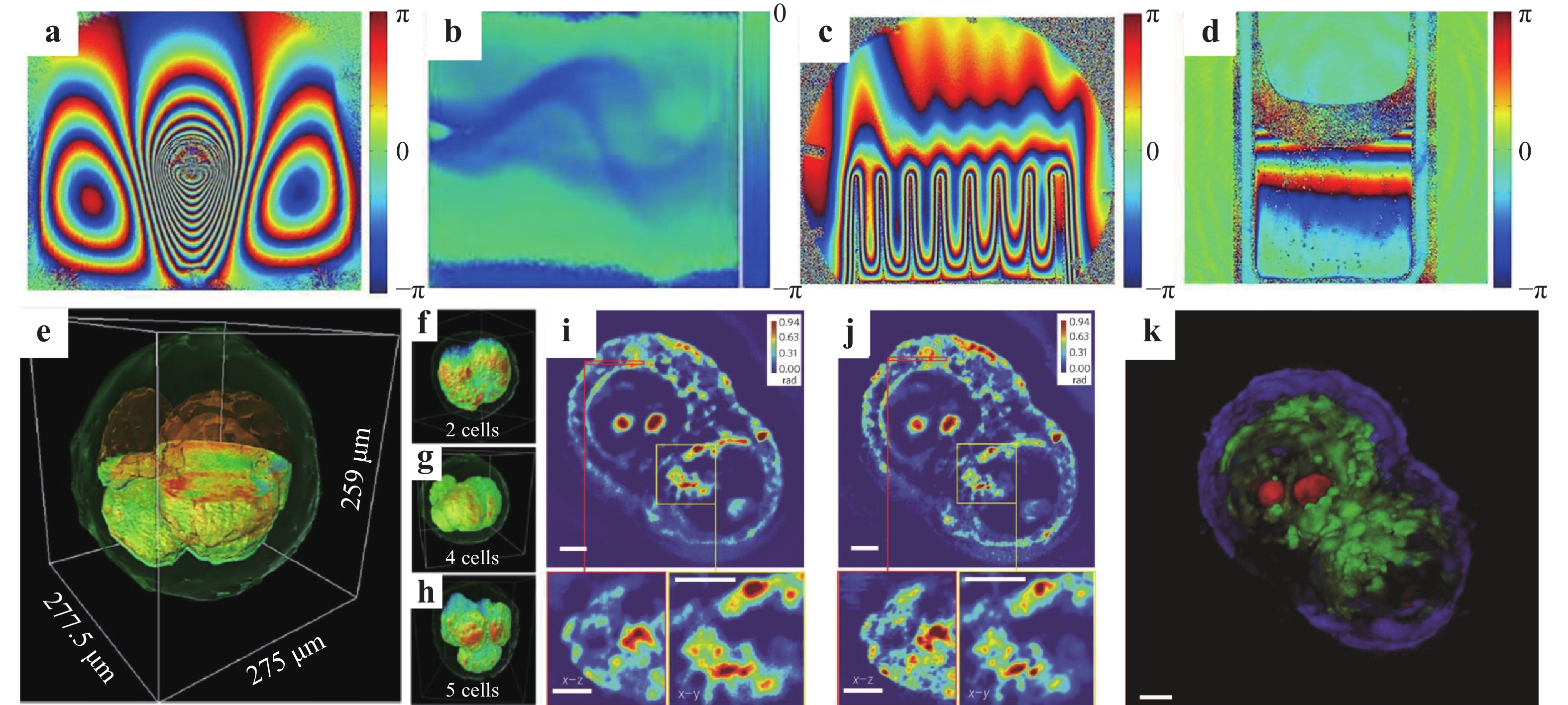
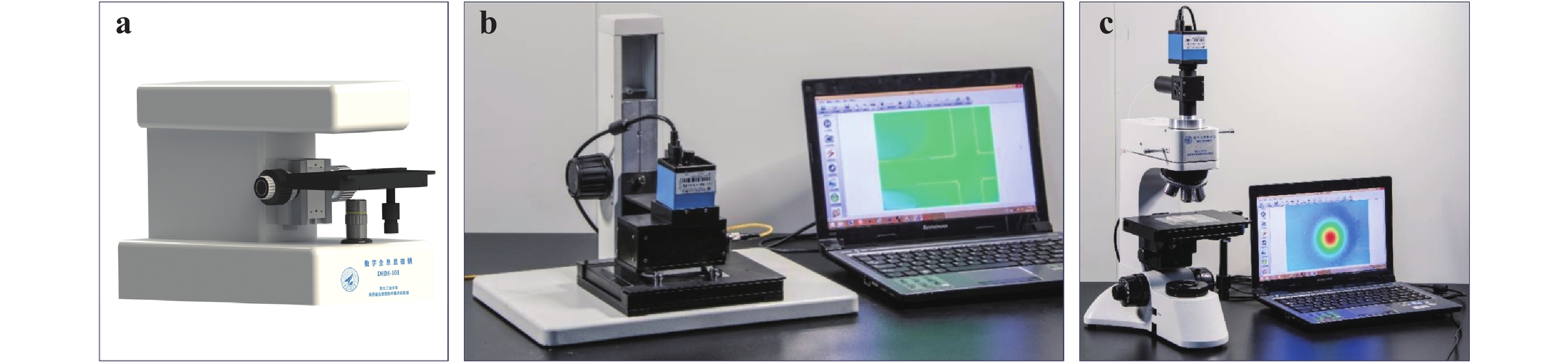
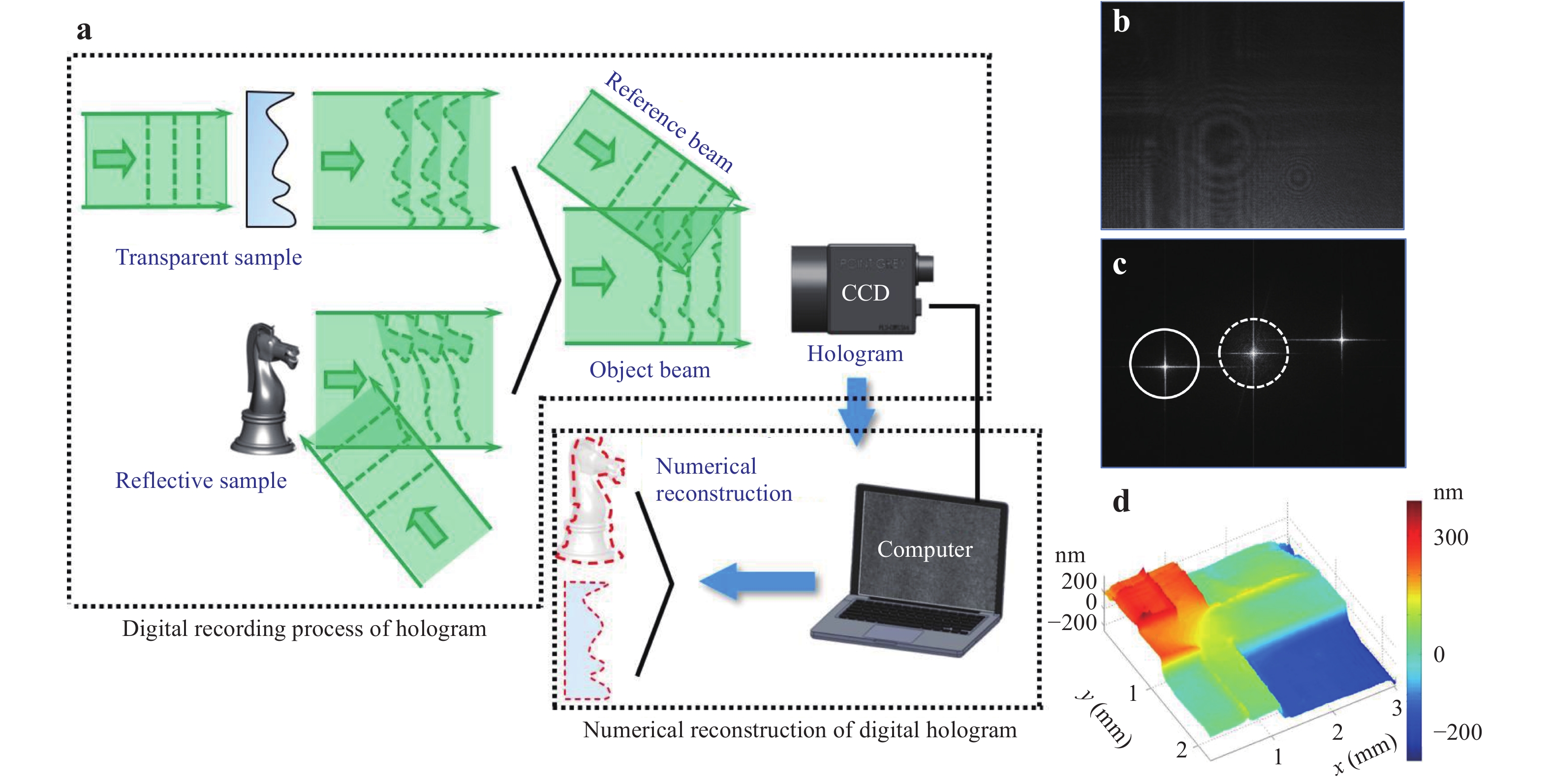
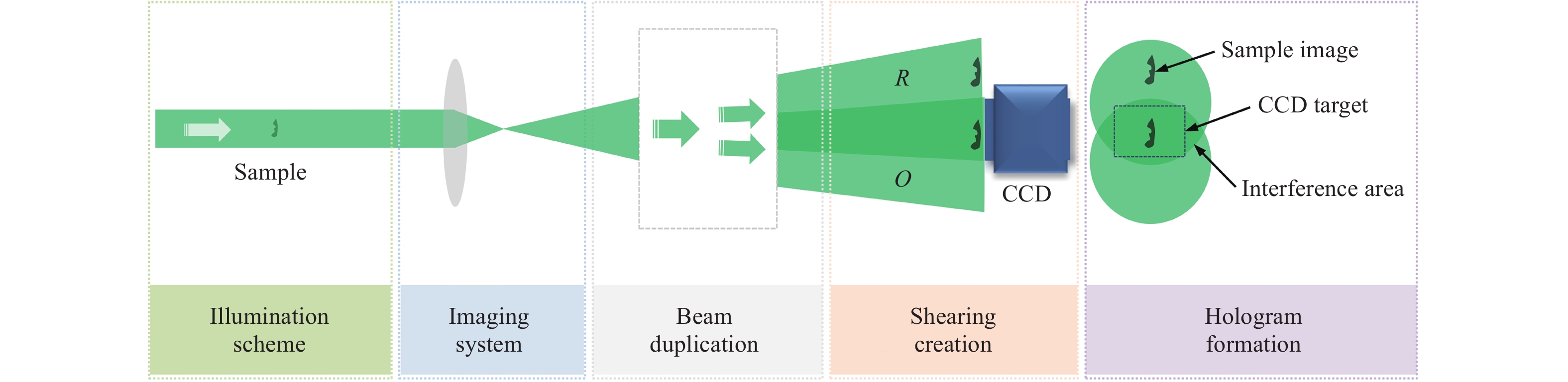
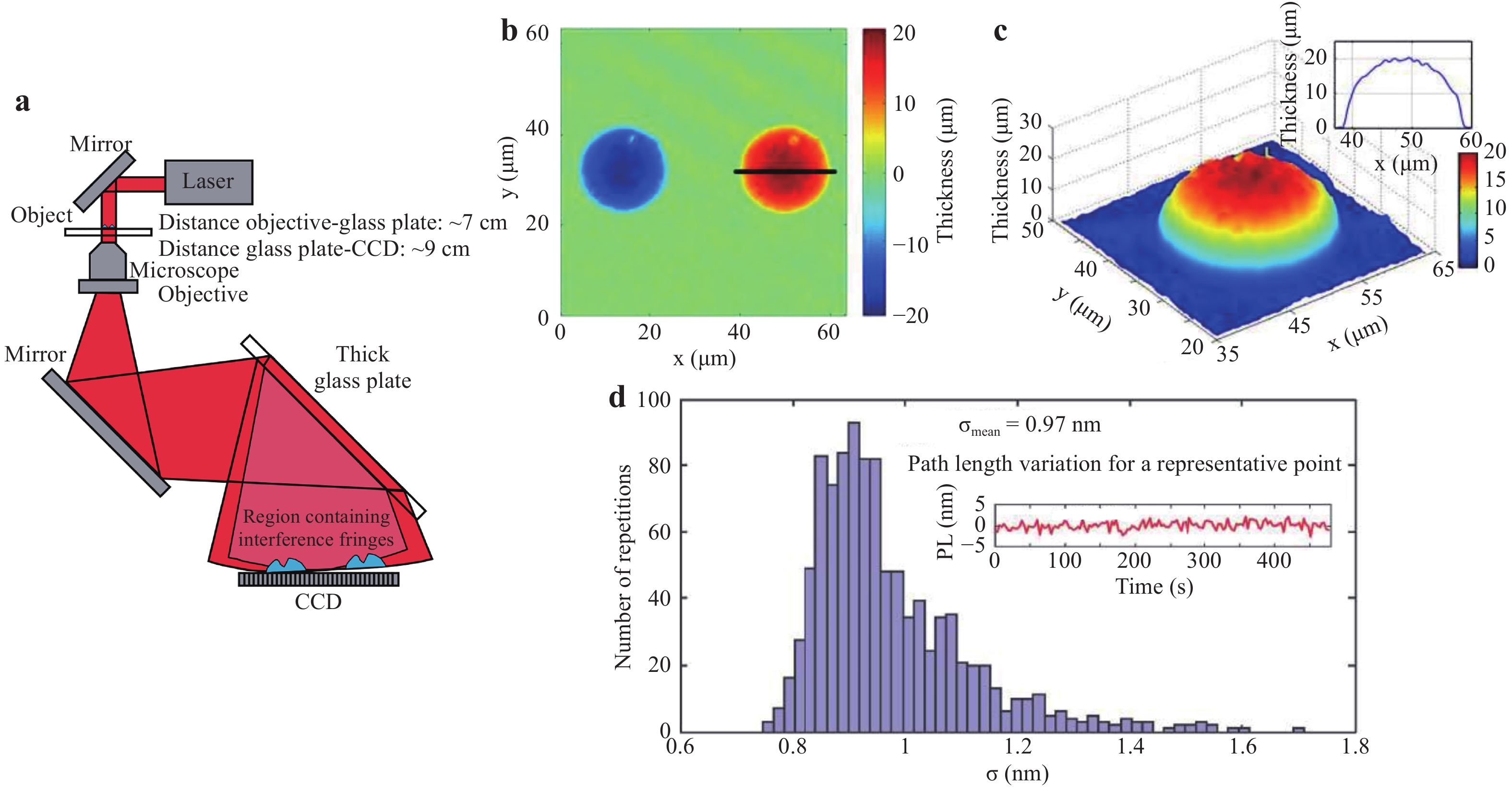
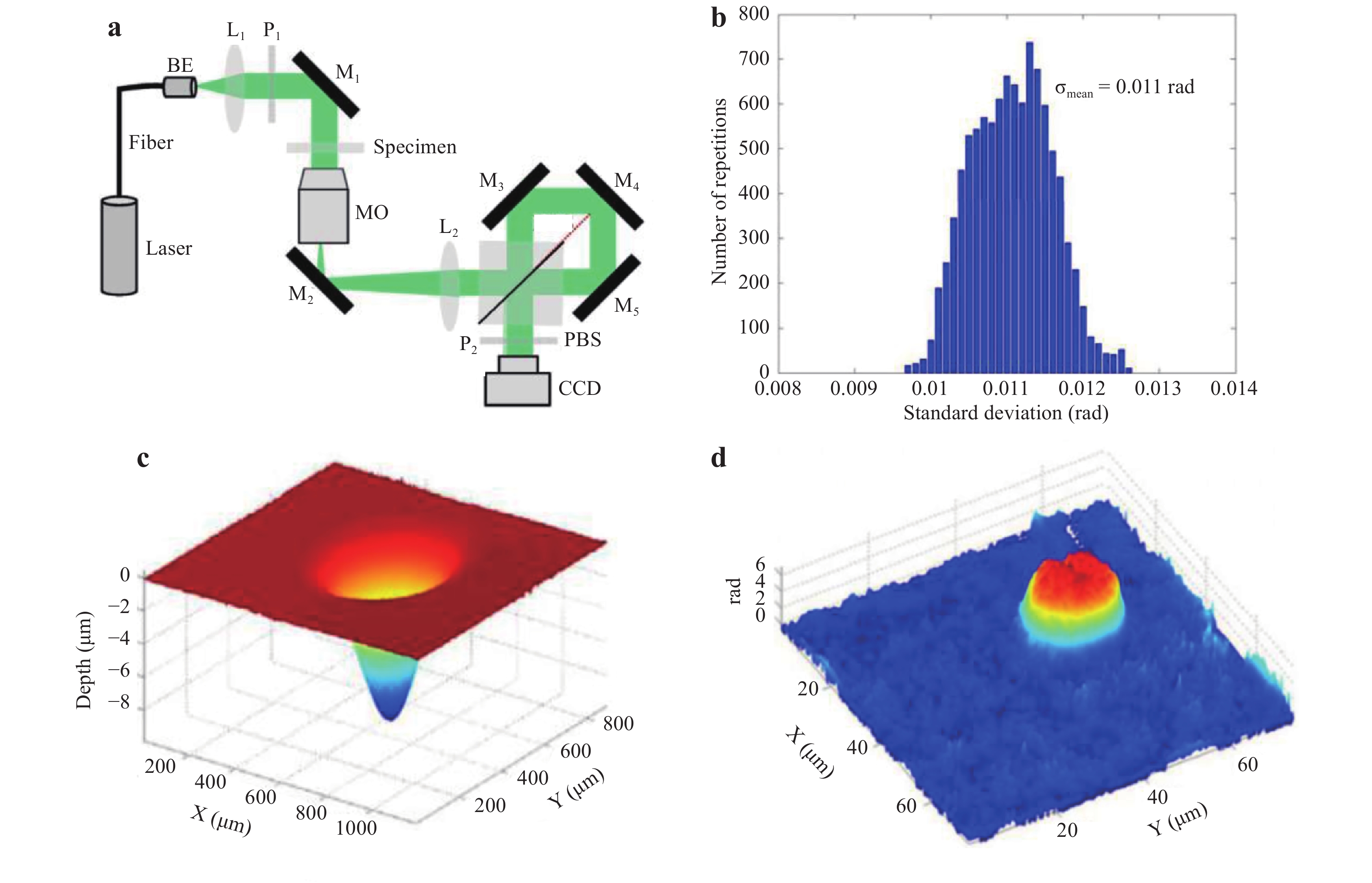
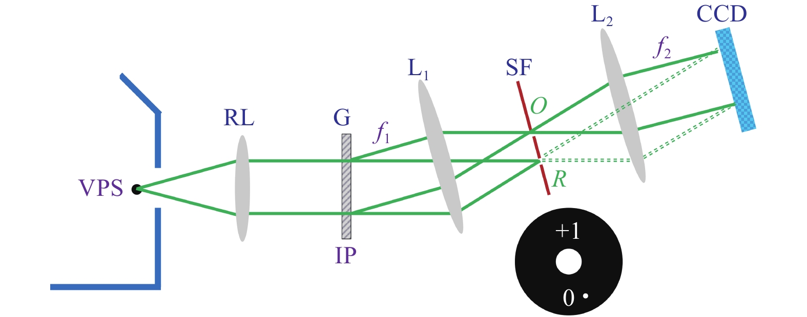
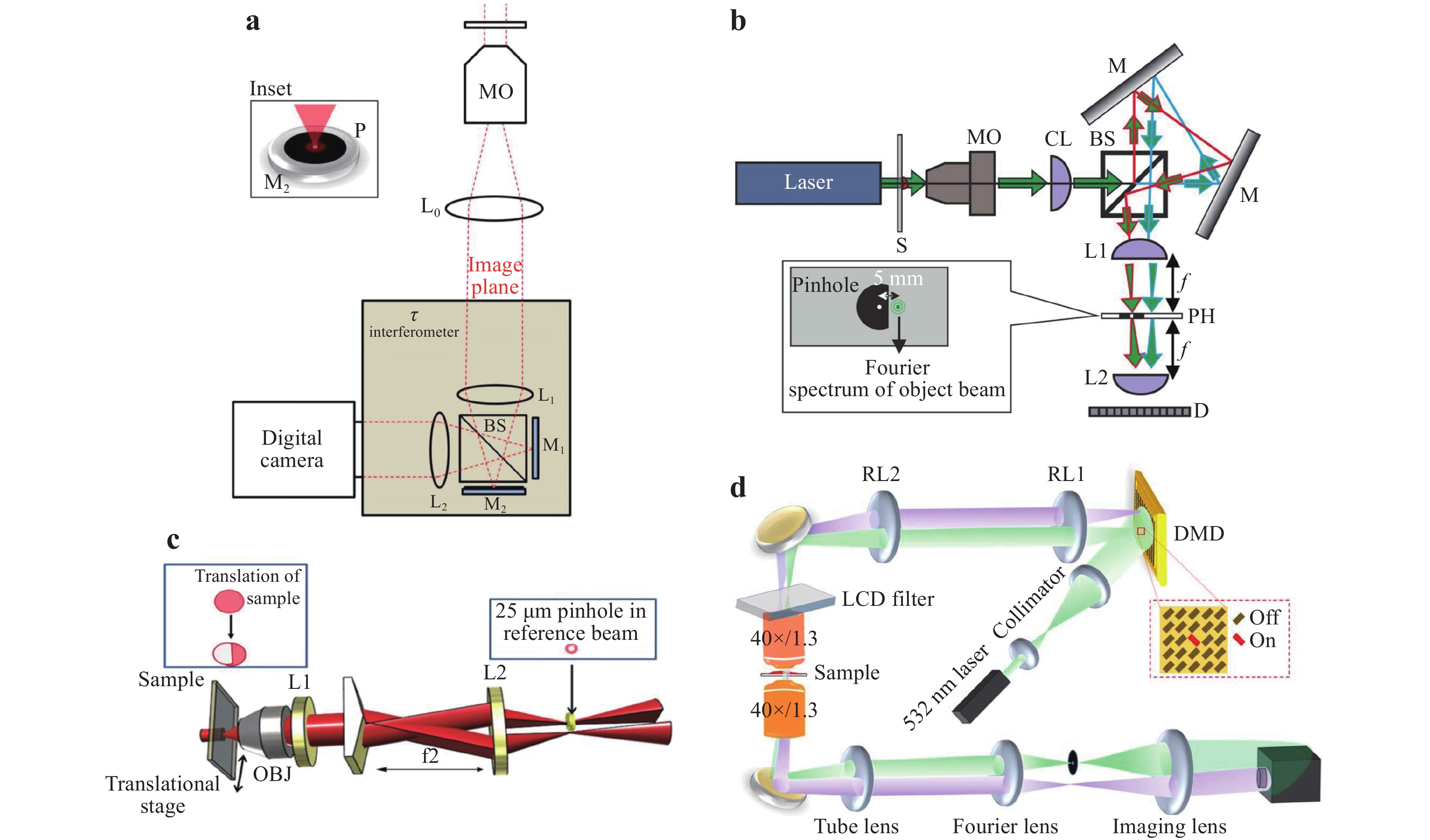
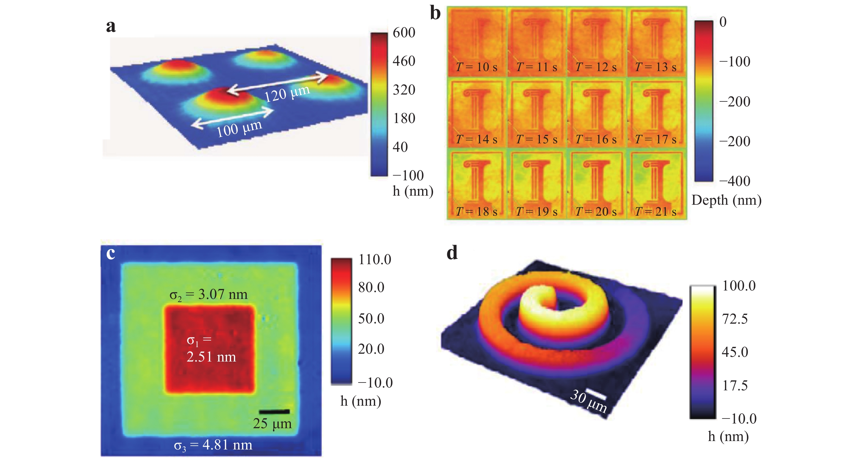
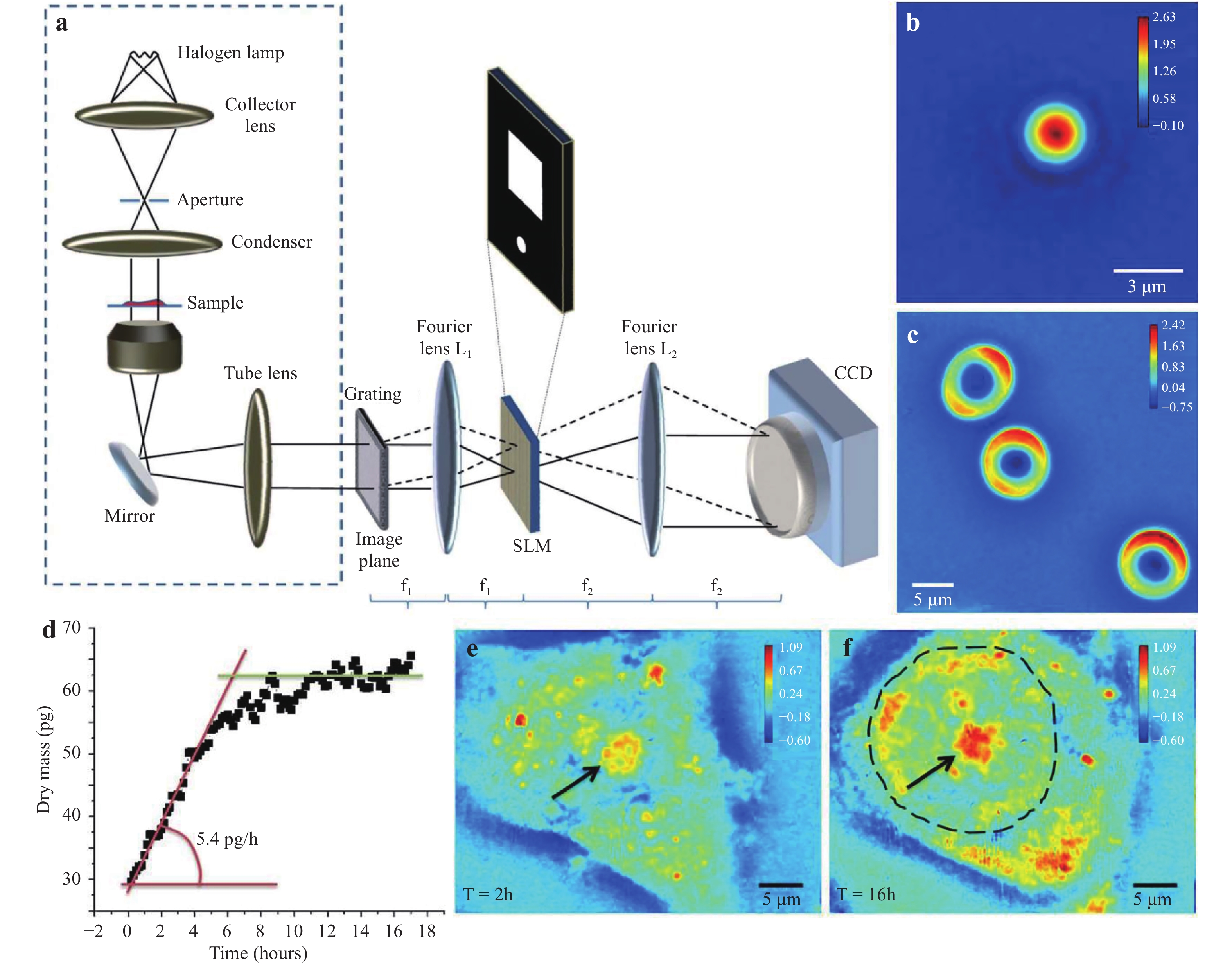
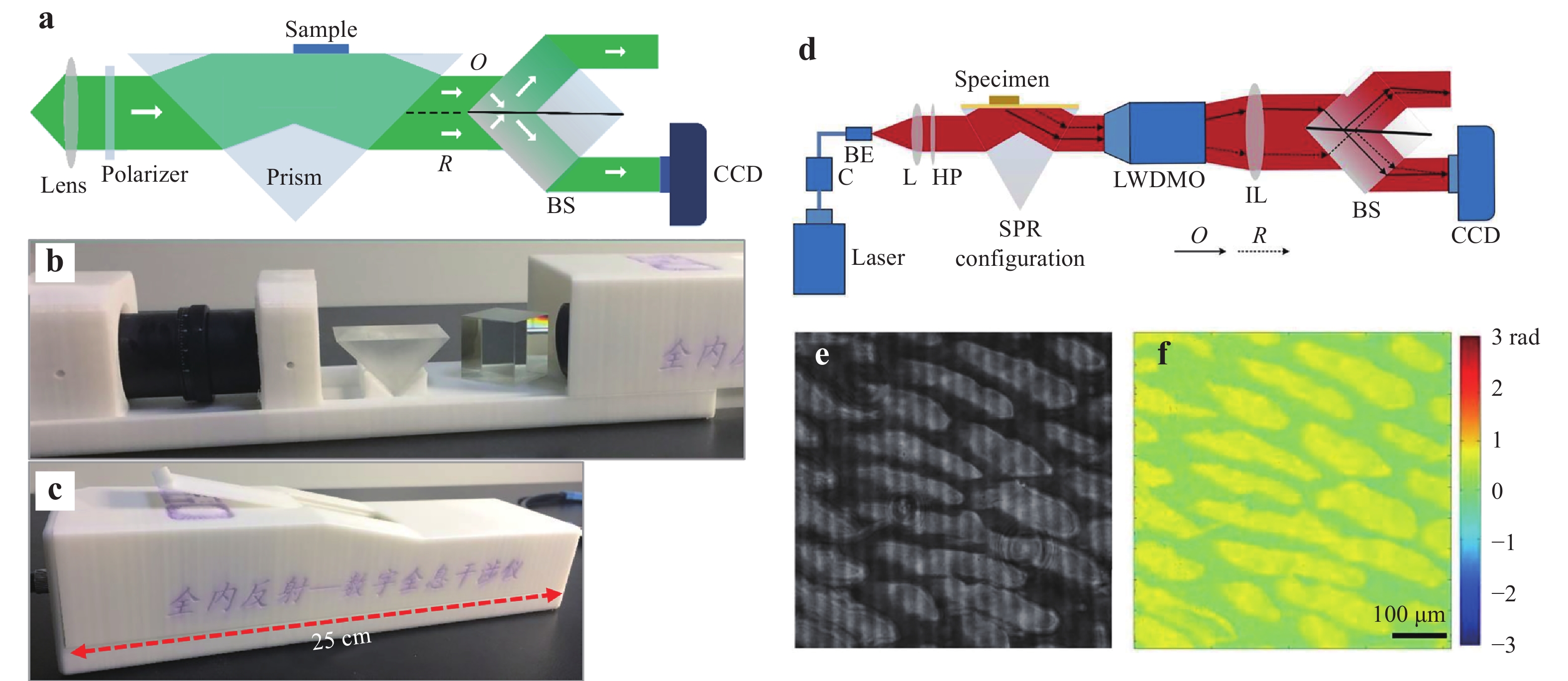
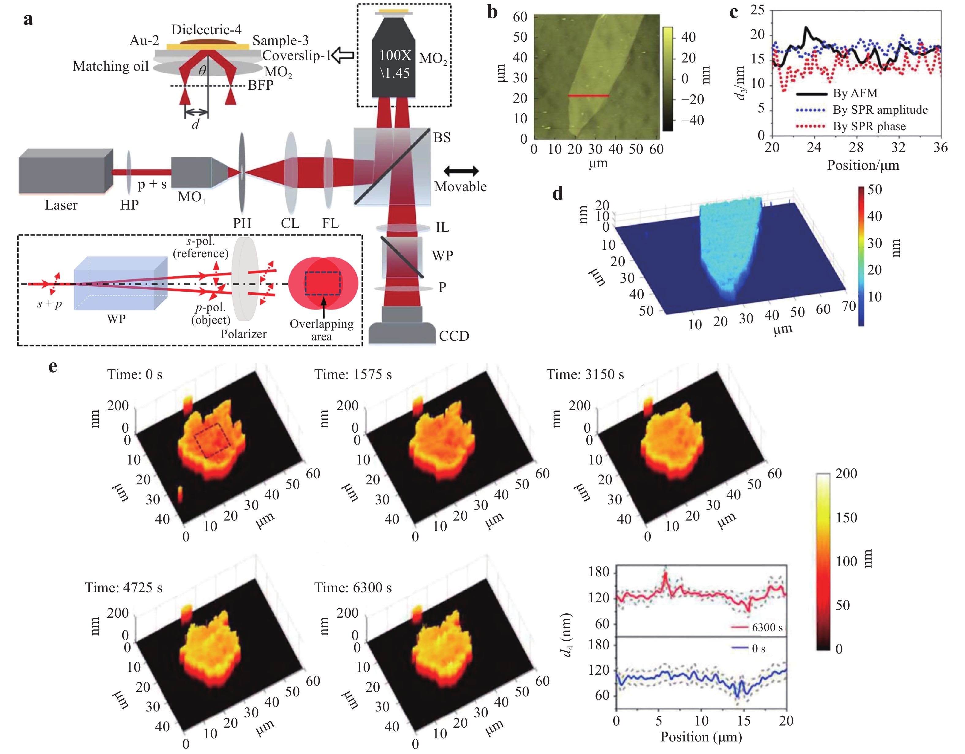
Digital holography possesses the advantages of wide-field, non-contact, precise, and dynamic measurements for the complex amplitude of object waves. Today, digital holography and its derivatives have been widely applied in interferometric measurements, three-dimensional imaging, and quantitative phase imaging, demonstrating significant potential in the material science, industry, and biomedical fields, among others. However, in conventional off-axis holographic experimental setups, the object and reference beams propagate in separated paths, resulting in low temporal stability and measurement sensitivity. By designing common-path configurations where the two interference beams share the same or similar paths, environmental disturbance to the two beams can be effectively compensated. Therefore, the temporal stability of the experimental setups for hologram recording can be significantly improved for time-lapsing measurements. In this review, we categorise the common-path models as lateral shearing, point diffraction, and other types based on the different approaches to generate the reference beam. Benefiting from compact features, common-path digital holography is extremely promising for the manufacture of highly stable optical measurement and imaging instruments in the future.

Design and manufacture AR head-mounted displays: A review and outlook
Dewen Cheng, Qiwei Wang, Yue Liu, Hailong Chen, Dongwei Ni, et al.
Published. 2021, 2(3) : 350-369 doi: 10.37188/lam.2021.024
Augmented reality head-mounted displays (AR-HMDs) enable users to see real images of the outside world and visualize virtual information generated by a computer at any time and from any location, making them useful for various applications. The manufacture of AR-HMDs combines the fields of optical engineering, optical materials, optical coating, precision manufacturing, electronic science, computer science, physiology, ergonomics, etc. This paper primarily focuses on the optical engineering of AR-HMDs. Optical combiners and display devices are used to combine real-world and virtual-world objects that are visible to the human eye. In this review, existing AR-HMD optical solutions employed for optical combiners are divided into three categories: optical solutions based on macro-, micro-, and nanooptics. The physical principles, optical structure, performance parameters, and manufacturing process of different types of AR-HMD optical solutions are subsequently analyzed. Moreover, their advantages and disadvantages are investigated and evaluated. In addition, the bottlenecks and future development trends in the case of AR-HMD optical solutions are discussed.