HTML
-
Surface-enhanced Raman scattering (SERS) was first reported by Fleischmann et al. in 1974. An optical phenomenon associated with increased Raman signal intensity from roughened Ag electrodes was subsequently discovered by Van Duyne et al1−4. In the 1980s, two primary theoretical mechanisms were proposed to explain the SERS effect. The electromagnetic mechanism (EM) is based on the excitation of localized surface plasmon resonances (LSPRs) resulting from the collective oscillations of electrons on nanoparticles (NPs), while the chemical mechanism (CM) that is attributed to SERS involves a charge transfer (CT) process. Specifically, this involved the transfer of so-called “hot electrons” (i.e., a photocurrent) between the analyte molecules and the substrate material5. Both mechanisms are currently considered plausible, with the former being applied to explain SERS on noble metals and the latter being employed in the case of semiconductors. Theoretically, a large SERS cross section can allow the detection of single analyte molecules6. However, it is difficult to experimentally demonstrate single-molecule detection, because real-world SERS substrates do not provide sufficiently high sensitivity. In the 2000s, so-called “hot spots” associated with LSPR coupling in nanogaps were observed when noble metals were used. These were used to significantly improve the sensitivity of SERS substrates and, in turn, the intensities of Raman signals7, 8. Since then, numerous strategies have been suggested for the fabrication of highly sensitive SERS substrates. Based on the proposed EM, there has been a focus on generating dense hot spots on SERS substrates to increase the number of excited molecules in these regions. Three-dimensional (3D) nanostructured SERS substrates are also attracting considerable attention, because hot spots can be created in significant numbers along the third axis of such structures9−11. A second approach is to control the location of hot spots to accurately excite target molecules. Research on the CM has explored advanced semiconductor materials such as two-dimensional (2D) graphene and MoS2 as a means of increasing photocurrents12, 13. Recently, several hybrid SERS substrates were also reported, including Au@ZnO, Ag@TiO2, and Ag@Si, which have shown impressive SERS enhancement because of the synergistic effects of the EM and CM14−16. Unfortunately, the enhancement factors (EFs) obtained in experimental SERS studies conducted till date have not exceeded 1010, which is equivalent to a detection limit of approximately 10−9 M (approximately 1 nM, depending on the measuring condition), as listed in Table 1. This performance is inferior to the theoretical prediction. Thus, achieving higher EFs is a significant challenge related to the development of SERS; consequently, new strategies are required to achieve EFs higher than 1010.
SERS substrate Analyte EF Detection limit Ref. Au nanowire Oligonucleotide 5.5 × 10⁵ 10−9 M 17 Au nanostructure Oligonucleotide 1.49 × 10⁶ 18 Au-capped Si metastructure Rhodamine 6G (R6G) 5.67 × 10⁴ 10−6 M 19 Au sphere monolayer 2-naphthalenethiol 5.4 × 10¹⁰ 10−13 M 20 Au film 4-mercaptophenylboronic acid 1.01 × 10⁶ 10−5 M 21 Au nanoparticle composite Thioaniline 2.7 × 10⁶ 22 Ag nanoparticle composite R6G 2.4 × 10⁷ 10−8 M 23 Au nanoparticle 4-mercaptothiophenol 2.9 × 10⁷ 24 Au nanostructure R6G 8 × 10⁷ 25 Table 1. List of enhancement factors and detection limits using noble metal materials as reported in 2020.
SERS substrates can be approximately classified into three categories: nanostructured substrates, NP colloids, and hybrid 3D substrates, as shown in Fig. 1. Nanostructured substrates typically include the arrays of patterned nanospheres, nanotips, nanowires, and nanopyramids26−31. These substances can be fabricated by top-down methods, including energy beams (ion, electron, and laser beams), subtractive processing, and plasma/chemical etching. Bottom-up methods such as 3D additive manufacturing, chemical vapor deposition, and sputter coating can also be used32−34. As an example, Fig. 1a shows a periodic surface structure fabricated by pulsed laser processing35. The electric field is significantly enhanced in these nanogrooves, which is critical for achieving high SERS signal intensity. The second category of SERS substrates comprises NP colloids consisting of nanospheres, nanostars, nanorods, nanoflowers, or nanodisks36−40. Fig. 1b shows Ag nanoplates with wavy edges synthesized using a wet chemical method. When compared to nanoplates with straight edges, the EF values obtained from nanoplates with wavy edges are increased by an order of magnitude, because the in-plane dipole resonance of such plates is red-shifted to match the excitation wavelength41. The third category of SERS substrates consists of hybrid 3D materials. As shown in Fig. 1c, a Si nanowire array fabricated by metal-assisted chemical etching can be used as a backbone to establish a SERS substrate on which Ag nanoparticles (AgNPs) are deposited42. The advantage of 3D substrates is that these materials permit light trapping, which increases the intensity of the SERS signal due to multiple reflections of light by the nanowire sidewalls.

Fig. 1
a Scanning electron microscopy (SEM) image of a periodically structured titanium surface35. © 2019 by John Wiley and Sons. b SEM image of nanoparticle colloids containing triangular Ag nanoplates with wavy edges41. Reproduced with permission from Willy-VCH. © 2013 by John Wiley and Sons. c SEM image of a Si nanowire array coated with Ag nanoparticles (AgNPs)42. © 2019 by Multidisciplinary Digital Publishing Institute.SERS sensors show significant potential for applications in diverse fields including the food industry, biotechnology, environmental monitoring, photocatalysis, and medical care43−48. Highly sensitive SERS substrates with low detection limits (< l nM) are required for practical applications; consequently, new strategies have been proposed in recent years to achieve femtomolar- to attomolar-scale sensing. The fabrication of highly sensitive SERS substrates through femtosecond laser processing is increasingly attracting attention owing to the versatility, flexibility, and high resolution of this process, together with the capacity to generate 3D substrates. In this review, we first introduce standard methods for evaluating the performance of SERS substrates. The calculation of EF values, which are the most significant performance indicators for SERS substrates, is also examined along with certain other relevant criteria. In the third section, femtosecond-laser-based techniques for the fabrication of SERS substrates are introduced. In the fourth section, recent strategies for enhancing SERS substrate performance with the goal of achieving attomolar-scale sensing are presented. In the fifth and sixth sections, we highlight aspects of SERS applications in real-time sensing based on microfluidic chips and biotechnology for cell imaging, deoxyribonucleic acid (DNA) sequencing, and cancer screening. The last section presents a summary and the future outlook for SERS and its potential applications.
-
Typically, SERS substrates are composed of either nanostructured metals or NP colloids. Owing to the diversity of these substrates, it is difficult to define an ideal criterion for the comprehensive evaluation of performance. However, SERS performance is primarily governed by the detection ability during analyses using Raman spectroscopy. Thus, the spatial and spectral resolutions of the spectrometer, as well as its light-collecting ability, are critical for achieving a low detection limit49. The measurement parameters employed during SERS sensing, together with the pretreatment of the SERS substrate, also affect the performance. These measurement parameters include the power, spot size, and wavelength of the Raman excitation laser, acquisition time, and spectrometer resolution. During SERS analysis, the analyte molecules are typically transferred to the substrate and may be subsequently incubated to increase the bonding strength and analyte quantity. SERS performance is also affected by factors such as the spatial distribution, surface orientation, molar mass, and scattering cross section of the analyte molecules. Therefore, it is impossible to provide a common definition of SERS performance. Nevertheless, there are several criteria that can be used to compare the performance of SERS substrates.
-
In most applications, the SERS substrate should have the highest possible sensitivity. The EF is the most common means of quantitatively evaluating this sensitivity and can be calculated using either Eq. 1 or 10. In the first approach, the EF is calculated based on the number of excited molecules in the sample area that is exposed to laser radiation, which is formulated as15, 50−53
$$EF = ({I_{SERS}}/{N_{ads}})/({I_{or}}/{N_{or}})$$ (1) where ISERS is the Raman signal intensity obtained from analyte molecules attached to the SERS substrate, Ior is the ordinary Raman signal intensity (i.e., the intensity obtained from a standard substrate such as glass), Nads is the number of excited analyte molecules adsorbed on the SERS substrate, and Nor is the number of molecules excited using the ordinary Raman process. The ISERS and Ior values can be directly obtained from experimental data. Nads is calculated as
$${N_{ads}} = {u_M} \cdot {u_S} \cdot {A_M}$$ (2) where uM is the surface density of the nanostructures/NPs forming the SERS substrate, uS is the surface density of the analyte molecules on the substrate, and AM is the surface area of the nanostructures/NPs. Nor is calculated as
$${N_{or}} = {C_{or}} \cdot {A_{or}}$$ (3) where Cor is the volume density of the molecules used for ordinary Raman analysis and Aor is the effective height of the scattering volume of the analyte. In the case of 3D SERS substrates, the laser focusing volume should be considered because the molecules show a 3D distribution and they may be effectively excited throughout the entire laser focusing volume. The laser focusing volume (Vlaser) and area (Slaser) can be calculated as
$${V_{laser}} = 2 \cdot \int_0^{{Z_R}} \pi \left({w_0}\sqrt {1 + {{\left(\frac{{{\lambda _Z}}}{{\pi {w_0}}}\right)}^2}} \right){^2}dz$$ (4) and
$${S_{laser}} = \pi \cdot w_0^2$$ (5) where ZR is the Rayleigh range, i.e.,
$${Z_R} = {S_{laser}}/\lambda $$ (6) and w0 is the beam waist, i.e.,
$${w_0} = (\sqrt 2 \lambda )/(\pi \tan (\theta ))$$ (7) Here, λ is the laser wavelength and θ is the apex angle.
If the SERS analysis proceeds according to the EM, which implies that the molecules are only effectively excited in hot spots, then the area of the substrate occupied by hot spots, Shotspot, should be considered. This value is calculated as
$${S_{hotspot}} = \sqrt R d$$ (8) where R is the average radius of the nanostructures/NPs and d is the distance between two adjacent nanostructures/NPs. On this basis, Eq. 2 can be transformed to
$${N_{ads}} = {S_{hotspot}}/{S_{molecule}}$$ (9) where Smolecule is the area over which the analyte molecules are deposited in the laser focal volume, Vlaser.
Although Eq. 1 is widely used to calculate the EF, it suffers from several problems. Specifically, the exact surface area of the SERS substrate is difficult to ascertain. In addition, to estimate the number of excited analyte molecules, it is necessary to assume that the molecules on the SERS substrate are uniformly attached and that all molecules in the hot spots are excited; consequently, the EF is typically overestimated. These issues also result in low reproducibility of EF values among different studies. To address these challenges, another definition for the SERS EF was proposed, known as the analytical EF (AEF), which is calculated as
$$AEF = ({I_{SERS}}/{C_{SERS}})/({I_{or}}/{C_{or}})$$ (10) where ISERS is the intensity of the SERS signal obtained from the analyte molecules, CSERS is the analyte concentration used for the SERS analysis, Ior is the intensity of the ordinary Raman signal obtained from the analyte molecules, and Cor is the concentration employed for the ordinary Raman analysis. ISERS, Ior, CSERS, and Cor can be directly obtained from experimental data; thus, if all experimental procedures are clearly provided, repeatable AEF values can be ensured. However, the AEF ignores the surface effect that may be associated with SERS, such as the distance between the molecules and the substrate, because it uses the analyte liquid concentration instead of the number of molecules on the substrate surface.
In addition to Eq. 1 and 10, there are several other approaches for calculating EF. For example, if an analyte generates significant background fluorescence in response to laser excitation, the analyte may produce different Raman signals during SERS and ordinary Raman analyses owing to a resonance effect. In such cases, EF can be simply determined by calculating the ratio of ISERS to Ior as54
$$EF = ({I_{SERS}}/{I_{or}})$$ (11) If the applied excitation laser power differs between SERS and ordinary Raman experiments, this power variation should also be considered. Thus, the equation is modified to55
$$EF = ({I_{SERS}}/{I_{or}})({C_{or}}/{C_{SERS}})({P_{or}}/{P_{SERS}})$$ (12) where PSERS and Por are the excitation laser powers for SERS and ordinary Raman analyses, respectively.
Assuming that the SERS effect originates solely from LSPR and neglects the chemical enhancement effect on the metal substrate (i.e., the EM mechanism is dominant), the enhancement can also be directly obtained from the enhanced electric field as56
$$EF = {\left| {\frac{{{E_{loc}}({\lambda _{exc}}){E_{loc}}({\lambda _{Raman}})}}{{{E_{inc}}({\lambda _{ect}}){E_{inc}}({\lambda _{Raman}})}}} \right|^2}$$ (13) where Eloc(λexc), Eloc(λRaman), Einc(λect), and Einc(λRaman) are the localized (enhanced) and incident electric fields at the excitation laser and Raman wavelengths λexc and λRaman, respectively. Normally, λexc is close to λRaman57, 58. Therefore, the enhancement is approximately equal to the fourth power of the localized electric field, which implies that we can write this as
$$EF = {\left| {\frac{{{E_{loc}}}}{{{E_{inc}}}}} \right|^4}$$ (14) The electric field enhanced by metal nanostructures can be numerically simulated. Fig. 2 shows the electric field distribution in a Cu-Ag layered nanodot array with a height of 250 nm, diameter of 200 nm, and a distance of 50 nm between nanodots, simulated by the finite element method59. The polarization direction of the excitation light is parallel to the nanodot array and substrate. Owing to the significantly short distance between neighboring nanodots (50 nm), strong, localized, and high-density hot spots are generated between each metal nanodot, which will increase the EF.
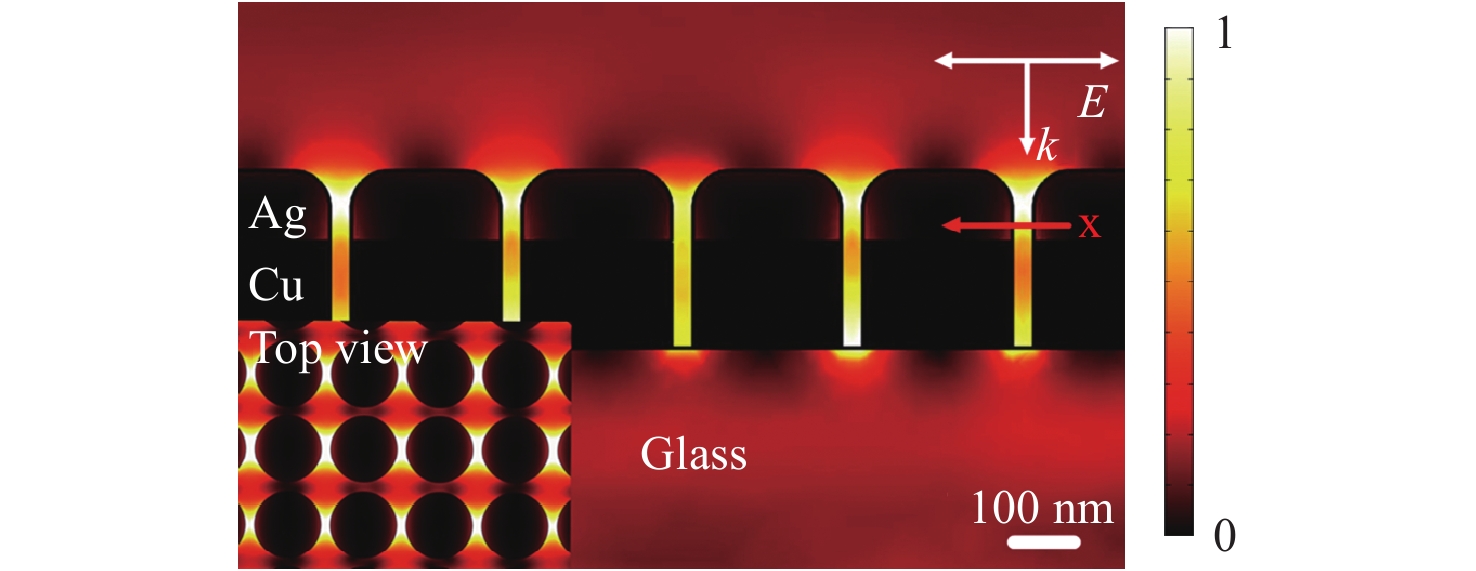
Fig. 2 Simulation of the near-field electric field distribution in a two-dimensional (2D) periodic Cu-Ag layered nanostructure at 633 nm (inset: top view of the simulated electrical field intensity distribution).
The polarization direction of the excitation light is parallel to the plane of the nanodot array and substrate59. Reproduced with permission from WILEY-VCH. © 2018 by John Wiley and Sons.For certain applications, the EF value is not as important as the low detection limit. For example, in the case of cell imaging, NPs are labeled with biomarkers and transferred into cells, after which Raman mapping based on the biomarkers generates Raman spectra that provide images of the cells. In this scenario, the lower detection limits obtained using SERS substrates provide improved spatial resolution. Thus, the detection limit for SERS analysis is vital for sensor applications. Even so, it is not advisable to simply compare the detection limit as a way of assessing performance, because the detection limit can be significantly affected by the capabilities of the spectrometer itself, especially the light-collection efficiency.
-
When evaluating SERS substrates, the EF and detection limit are the primary criteria, although there are secondary criteria, including reproducibility, reusability, lifetime, and surface plasmon modulation.
The reproducibility of a SERS substrate is an indicator of the reliability of the material for SERS applications, and the relative standard deviation (RSD) can be used to describe this factor. Generally, colloids show superior RSD values as SERS substrates, because their shape and size can be strictly controlled by using wet chemical synthesis procedures. This, in turn, improves the reproducibility of the SERS analysis to achieve RSDs of less than 5%. In contrast, the RSDs for nanostructured substrates typically range between 5 and 10%. Although periodic nanostructures were originally developed to increase uniformity, it is significantly challenging to fabricate these structures over large metal surfaces with a resolution that is better than 100 nm. In addition, reusable SERS substrates with a long lifetime are desirable in terms of reducing cost. As the analyte molecules are still adsorbed on the substrate after the analysis, these substrates must undergo post-treatment to remove the analyte before reuse. Common methods of cleaning substrates include acid washing (which promotes the detachment of analyte molecules) and self-cleaning (through photodegradation or electrochromic regeneration)29, 60−62. The lifetime of the SERS substrate is also an important factor for practical use. The typical lifetime of SERS substrates is only less than a couple of months owing to the oxidation of metal in ambient air. The SERS substrates using Ag have a shorter lifetime of approximately 1 month when compared to the 1.5 – 2 months for a substrate using Au. A protective material (antioxidant) added on the SERS substrates is effective for extending the lifetime to several months29, 63. Surface plasmon modulation is a significant indicator of SERS sensitivity, as the Raman excitation wavelength close to the LSPR should be used to achieve the best performance of SERS substrates. The easiest method for the modulation is to select the material of the SERS substrate to match the Raman excitation wavelength. For example, Al is suitable for excitation by ultraviolet (UV) light, Ag is suitable for SERS in the range of 400 – 1000 nm, and Au and Cu support SERS in the range of 550 – 1250 nm64. A more sophisticated method to modulate surface plasmons is to establish special structures such as plasmonic superlattices, based on which the surface plasmon of the SERS substrate can be tuned from near UV to near infrared. As shown in Fig. 3, the Au plasmonic superlattice with different lengths ranging from 400 to 1600 nm can modulate the resonant wavelength for surface plasmons from 700 to 2400 nm65.

Fig. 3
a SEM micrographs of Au nanoparticle arrays with different lattice parameters: from left to right, lattice length (L) = 400, 500, 600, 740, and 1600 nm. Scale bar: 1 μm. b Extinction spectra, normalized to the maximum, of Au nanocluster arrays with different lattice parameters65. Reproduced with permission from ACS. © 2018 by American Chemical Society.
Enhancement factor and detection limit of SERS substrate
Other criteria
-
Lasers are widely used for the fabrication of SERS substrates based on either nanostructured metal surfaces44 or metal NP colloids37. In the case of a nanostructured metal surface, the gap between the nanostructure features is one of the most important factors related to SERS performance, as the electric field enhancement is significantly affected by this distance. Specifically, distances narrower than 100 nm allow hot spots to be generated in these nanogaps owing to the coupling of the dipole resonance66, 67. Narrower nanogaps also produce greater enhancement of the electric field, indicating higher sensitivity. Therefore, a high degree of resolution is preferable during the fabrication of a SERS substrate. Femtosecond laser processing is a useful method of manufacturing nanoscale structures owing to its unique characteristics, including ultrashort pulse widths and significantly high peak intensities. Specifically, ultrashort pulse widths can suppress the formation of heat-affected zones around the processed area so as not to deteriorate the fabrication resolution, while the exceptionally high peak intensity can induce multiphoton absorption in transparent materials. The multiphoton absorption can further improve the spatial resolution in excess of the diffraction limit68. Another feature of femtosecond laser processing is the accurate and flexible control of processed regions both on the surface and in the volume of materials in ambient conditions using mechanical and optical components. Importantly, these unique characteristics of femtosecond lasers allow the fabrication of SERS substrates on flexible substrates69 as well as in closed microfluidic channels70. The former offers low-cost and easy-to-operate characteristics for certain important applications, including portable Raman spectroscopes for point-of-care diagnostics, while the latter can perform real-time sensing of a significantly small quantity of substances. In this section, we introduce three representative methods based on femtosecond laser nano-processing for the fabrication of SERS substrates.
-
Multiphoton absorption is a nonlinear process in which multiple photons can collaborate to excite a single electron, even if the bandgap of the material being irradiated is larger than the photon energy. This nonlinear absorption process requires a high photon density in both the space and time domains, which can readily be provided by a femtosecond laser. Multiphoton absorption combined with the threshold effect can improve the fabrication resolution to approximately 100 nm even when using a near-infrared wavelength71, 72.
Fig. 4a illustrates a diagram of the optical setup for the writing of Ag nanowires (AgNWs) using a femtosecond laser, as proposed by Mackenzie et al73. In this setup, a charge-coupled device camera (not shown) is used to monitor the fabrication process in real time. The femtosecond laser is focused through the objective lens of a microscope onto a target surface immersed in the Ag precursor under a slip glass. This forms an Ag nanostructure on the substrate surface by laser-induced multiphoton absorption based on direct writing (Fig. 4b). The associated reaction is as follows:
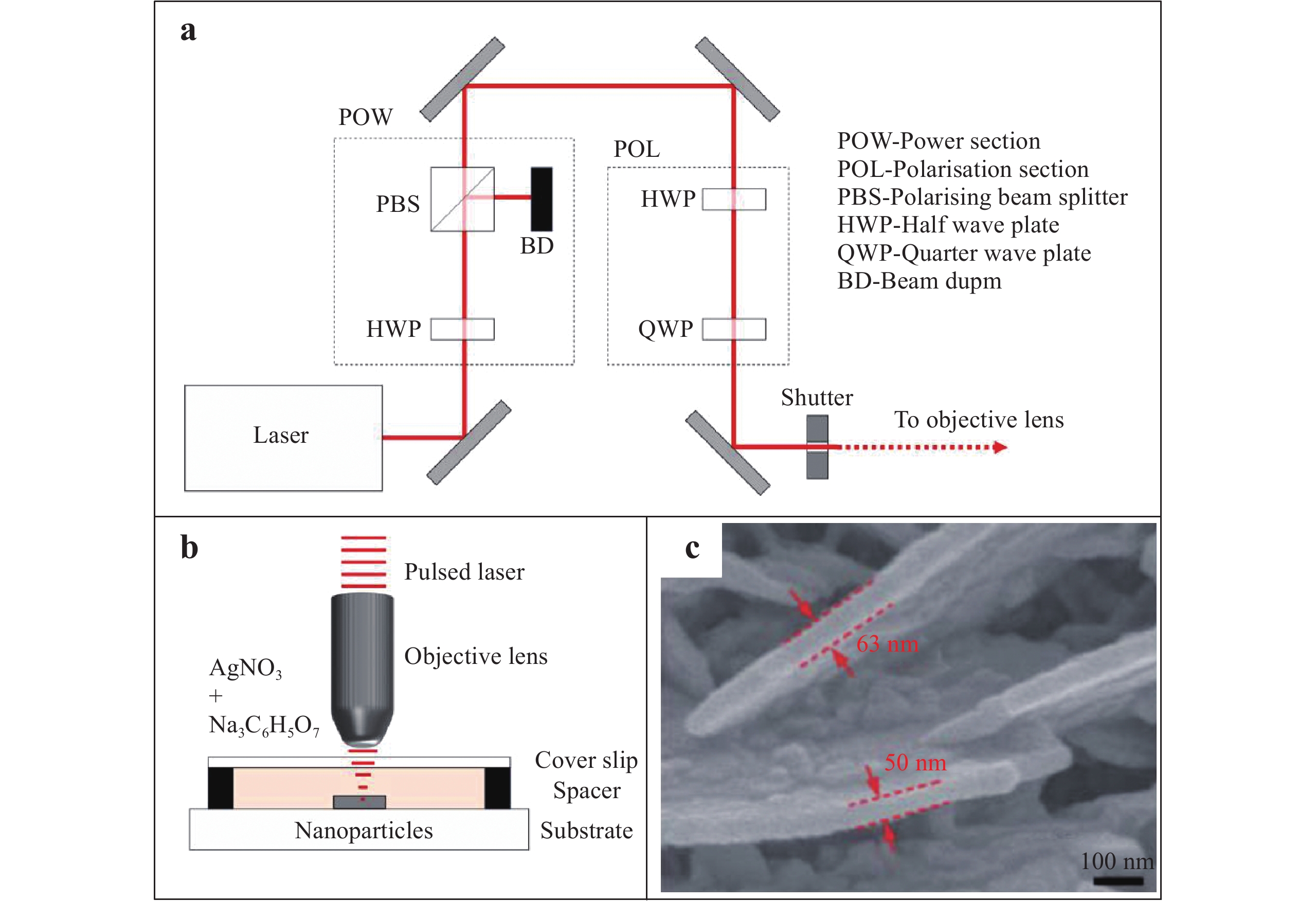
Fig. 4
Diagrams of the a optical setup and b irradiation of a sample during the femtosecond laser direct writing of Ag nanowires (AgNWs)73. Reproduced with permission from author (s). © 2019 by author (s). c SEM image of an Ag nanoplate fabricated on a substrate through the femtosecond laser reduction of Ag ions74. Reproduced with permission from RSC. © 2011 by Royal Society of Chemistry.$$N{a_3}{C_6}{H_5}{O_7} + A{g^ + }\xrightarrow{{nhv}}N{a_3}{C_6}{H_4}{O_7} + Ag + {H^ + }$$ (15) Recently, Xu et al. employed a multiphoton reduction technique using an 800 nm femtosecond laser to fabricate Ag SERS substrates. In their work, the laser reduction of Ag ions generated SERS substrates composed of vertical Ag nanoplates (Fig. 4c). The formation of these nanoplates may be attributed to surface plasmon excitation, which accumulated electrons and reduced Ag+ ions at specific sites44. The magnified image in Fig. 4c indicates the formation of Ag nanoplates with widths of 20 – 80 nm. Subsequent experimental results demonstrated that these nanoplates allowed the detection of p-aminothiphenol with an EF of 4 × 10⁸ 74. In addition, the Ag nanoplates were self-assembled into a nanostructure, providing a sub-10 nm nanogap. The analyte molecules were trapped in the nanogap, leading to a detection limit of rhodamine 6G (R6G) as low as 30 fM75.
-
Periodic nanostructures (or nanoripples) with subwavelength features can be produced on metals, semiconductors, and dielectrics by irradiation with a linearly polarized femtosecond laser at a laser fluence near the ablation threshold. These features, termed femtosecond laser-induced periodic surface structures (LIPSSs)76, can be classified into two types: low spatial frequency LIPSS (LSFL) and high spatial frequency LIPSS (HSFL). The surface structuring process to obtain LSFL involves a period close to or marginally smaller than the femtosecond laser wavelength. On metal films, the formation of LSFL structures is believed to be a result of the interference between the incident light and the light scattered at the surface77. In contrast, the process to obtain a HSFL uses a period much smaller than the femtosecond laser wavelength (1/2 – 1/10 of the laser wavelength). The mechanism of HSFL structure formation is relatively complex and remains unclear. Several hypothetical mechanisms were proposed to explain the formation of nanoripples, including the excitation of surface plasmon polaritons, self-organization, and the generation of second harmonics78.
Fig. 5 shows the morphology of a silica surface following irradiation with five successive pulses of a femtosecond laser with a fluence of 4.5 J/cm2 at the beam center79. An LSFL structure is evident in the central area of the crater, while an HSFL structure was formed at the edge of the ablated area. Because the femtosecond laser had a Gaussian beam profile, the energy density at the center of the laser spot was higher than that at the edge; therefore, the threshold fluence for the formation of a HSFL structure was lower than that for an LSFL structure80. Nanoripples could be generated as a result of an incubation effect based on the application of multiple pulses, and this effect became more pronounced as the number of pulses increased81. The formation of homogenous nanoripples by femtosecond laser processing requires the optimization of the scanning speed, pulse repetition rate, and fluence. The nanoripple orientation is either perpendicular or parallel to the linear polarization direction of the laser, depending on the irradiation conditions as well as the material being treated. In addition, 2D periodic nanostructures can be obtained using double femtosecond laser pulses with a delay and orthogonal polarization, as shown in Fig. 6. Interestingly, geometries such as spheres (Fig. 6b) and triangles (Fig. 6c) as well as other features can be obtained through laser fluence and delay time82.
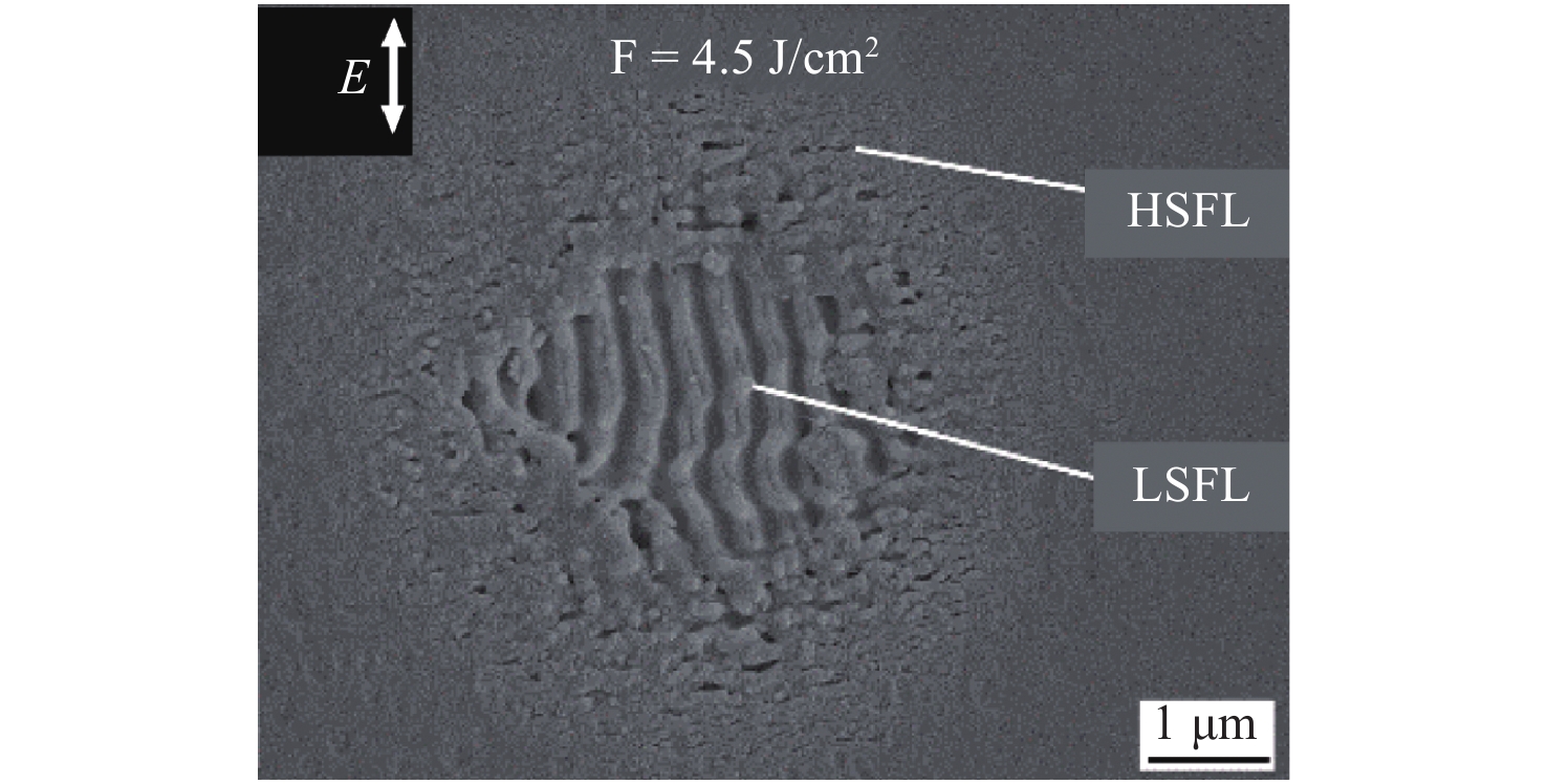
Fig. 5 SEM image of laser-induced periodic surface structures formed on a fused silica surface following the application of five femtosecond laser pulses79.
© 2018 by Multidisciplinary Digital Publishing Institute.
Fig. 6
a Diagram showing the formation of 2D periodic structures on a Co surface using two temporally delayed femtosecond laser pulses with orthogonal polarizations. Δt represents the delay time between the two beams, E1 and E2 are the polarization directions of the two beams, and F is the laser fluence. b Spherical shapes formed on the Co surface using Δt = 12 ps and F = 0.14 J/cm2. c Triangular shapes formed on the Co surface using Δt = 12 ps and F = 0.20 J/cm2 82. Reproduced with permission from AIP. © 2019 by American Institute of Physics Publishing.HSFL structures on metal surfaces can provide excellent SERS substrates because the periods in the range of 1/10 –1/5 of the incident femtosecond laser wavelength can be obtained, corresponding to approximately 80 – 200 nm. More importantly, nanogrooves with sub-50 nm widths can be generated within these nanostructures, and the electric field is significantly enhanced within these narrow grooves to produce hot spots. HSFL has already been employed in conjunction with SERS for molecular detection. Li et al. and Hamad et al. fabricated HSFL structures on Si surfaces decorated with AuNPs using femtosecond lasers and reported EF values of approximately 4.3 × 10⁷ and 1.5 × 10⁸, respectively83, 84. In addition, Bai et al. used an Ag HSFL structure for a SERS analysis85. Narrowing the nanogroove width will further enhance the electric field to achieve a higher EF. Recently, Lin et al. reported the use of two orthogonally polarized femtosecond laser beams in an overlapping manner to create a 12 nm groove on silicon86. Meanwhile, it is worth noting that the femtosecond laser can also generate hierarchical micro/nanostructures with HSFL87. Such hierarchical structures may improve SERS sensitivity owing to the coupling of hierarchies.
-
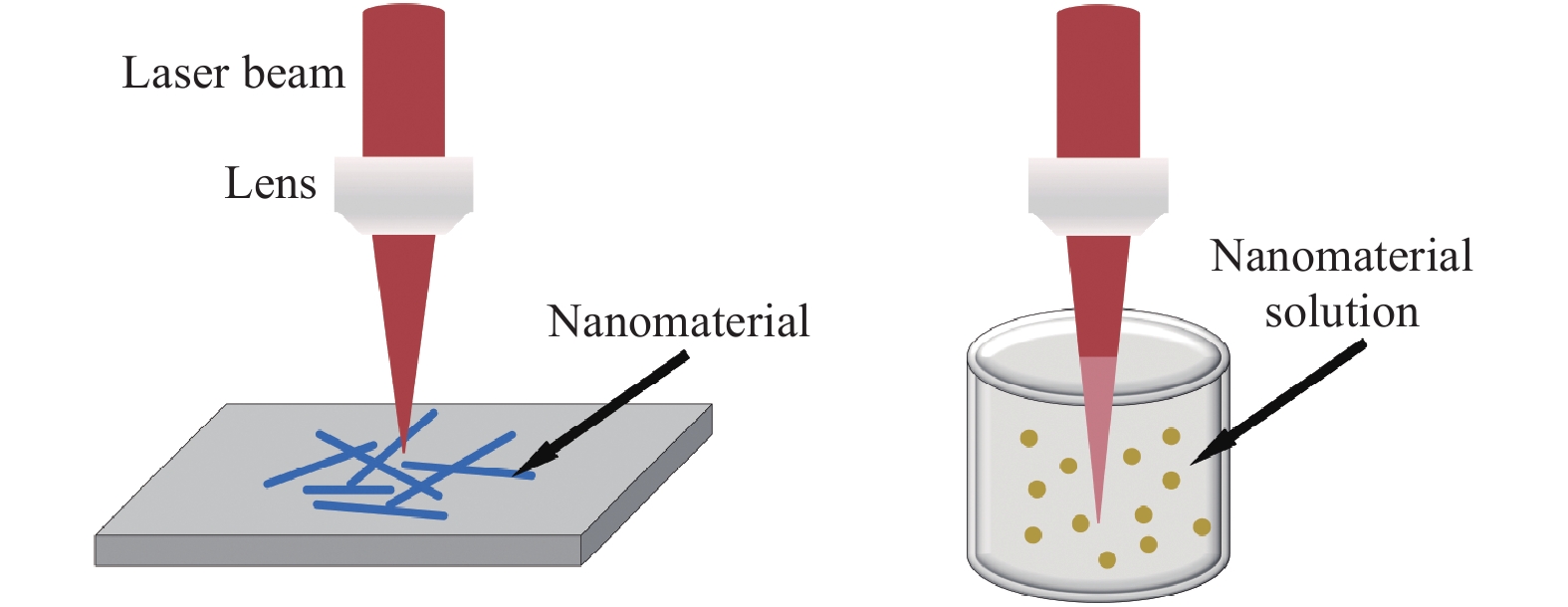
The femtosecond laser-induced localized melting of plasmonic nanomaterials for SERS has attracted significant attention in the past two decades. Fig. 7 shows two basic configurations of this technique, which can be performed not only on solid surfaces but also in liquids. The laser beam irradiation allows the localized melting of nanomaterials at specific locations on a nanoscale due to the photoexcitation of plasmons. When compared to the longer pulse duration laser, the advantage of the femtosecond laser is the minimal deformation of the nanostructures owing to the ultrashort pulse width88. This is crucial for the fabrication of SERS substrates, because the LSPR modes are highly dependent on the shape and size of the SERS substrate. As shown in Fig. 8a, irradiating the AgNWs on the amorphous carbon substrate using the femtosecond laser joined the two AgNWs at their junction. More importantly, two AgNPs were generated at the ends of the AgNW due to localized melting. The AgNPs at the end disturbed the distribution of the electric field along the AgNW and concentrated the electric field at their surfaces, as illustrated in Fig. 8b, c. Owing to the modulation of the electric field, the Raman scattering will be effectively enhanced when analyte molecules are absorbed at the NPs89. Similar results were also obtained during the femtosecond laser-induced nanojoining of AgNPs by localized melting. By focusing the femtosecond laser to a solution containing AgNPs, the adjacent AgNPs were joined to form Ag nanoclusters. The formed Ag nanoclusters contributed to the generation of hotspots, which enhanced the EF by approximately one order of magnitude90−92.

Fig. 8
a SEM image of localized melting AgNWs by using femtosecond laser to join each other at the junction. The ends of AgNWs were also melted to form AgNPs. Electric field distribution of b single AgNW and c AgNW with two AgNPs at the ends89. Reproduced with permission from AIP. © 2013 by AIP Publishing. -
Although femtosecond laser processing is still an expensive technology when compared to other conventional approaches used for SERS substrate fabrication, it is a promising tool for the preparation of high-performance SERS substrates because of its high controllability, high flexibility, and high reproducibility with a high fabrication resolution. When compared to the long pulse laser, the unique properties of the minimized thermal effect of femtosecond laser processing are beneficial for creating nanostructures on bulk materials. Importantly, femtosecond laser processing can create different types of nanostructures such as self-assembled nanoplates, HSFL, hierarchical micro/nanostructures, nanowires terminated with NPs, and nanoclusters in a well-controlled manner, as described above, which should enrich the SERS substrates depending on the applications. In addition, femtosecond laser processing can directly create nanostructures without lithographic processes, which significantly simplifies the fabrication procedure and reduces the number of process steps. In particular, 3D glass microfluidic SERS chips, which are described in Section 5, can be fabricated using the same femtosecond laser micromachining equipment without requiring complicated substrate stacking and bonding procedures or lithography for micro and nanostructuring, which can reduce the number of processes from more than 20 steps using standard semiconductor processing based on lithographic techniques to only 7 steps59. Nowadays, the femtosecond laser can fabricate sub-10 nm nanostructures through illustrated methods86, indicating their significant potential for fabrication of highly sensitive SERS substrates.
Femtosecond laser-induced multiphoton reduction
Laser-induced periodic surface structures
Femtosecond laser-induced localized melting of plasmonic nanomaterial
Advantages of femtosecond laser processing
-
Normally, the Raman cross section associated with label-free single-molecule sensing is smaller than 10−30 cm2sr−1 93. Although SERS can increase the Raman cross section, the typical detection limit remains at the nanomolar level. Two decades ago, the SERS substrates were elaborately designed and optimized, such as the factors of size, shape, and material types of NPs and nanostructures, to achieve a lower detection limit.94−96. For example, SERS sensing with a detection limit as low as 1 fM was demonstrated by hierarchical NPs synthesized by a seed-mediated growth by means of a galvanic reaction followed by chemical reduction97. Recently, several new strategies have been proposed to lower this limit to the attomolar level based on synergistic effects, including photo-induced enhanced Raman spectroscopy (PIERS), transient SERS, and liquid-interface SERS (LI-SERS).
-
The SERS phenomenon associated with semiconductor materials can be attributed to the CM associated with CT between the analyte and the substrate. In this process, the migration of hot electrons magnifies the Raman scattering cross section98, 99. The CT process can also be further amplified by pretreatment of the substrate with UV radiation, representing the PIERS technique, which increases the SERS intensity several times and can provide picomolar-level sensing100.
PIERS involves a hybrid system consisting of a noble metal and metal-oxide semiconductor materials. Typical components of hybrid systems include Ag and Au as the noble metals and TiO2, WO3, and ZnO as the semiconductors101. Increasing the UV exposure time was observed to exponentially increase the PIERS intensity. This technique is related to the formation of oxygen vacancies (Vo) that originate during the synthesis and post-treatment of the semiconductor material, because these atomic-scale defects promote Raman transitions. Combining a noble metal and semiconductor provides additional signal enhancement based on the EM. The metal-semiconductor interface also works to stabilize the formation of Vo by reducing the vacancy formation energy and increasing the charge carrier separation lifetime because of the presence of a Schottky barrier102.
Fig. 9 shows typical hot electron migration from a TiO2 substrate to Au/Ag NPs during the PIERS technique. Here, Vo defects are created in the TiO2 substrate in response to UV irradiation, which generate donor states below the bottom of the TiO2 conduction band. During the PIERS analysis, electrons are transferred from the Vo states to the TiO2 conduction band in response to the Raman excitation laser, and then to the Au/Ag energy levels. Electrons in the Vo states typically exhibit a slow decay with lifetime in the range of 30 – 60 min, which is sufficient to allow the collection of Raman data103. The PIERS effect can be quantitatively estimated based on the ratio of the densities of injected and initial electrons (ΔN/N) on the metal NPs, which is given as101
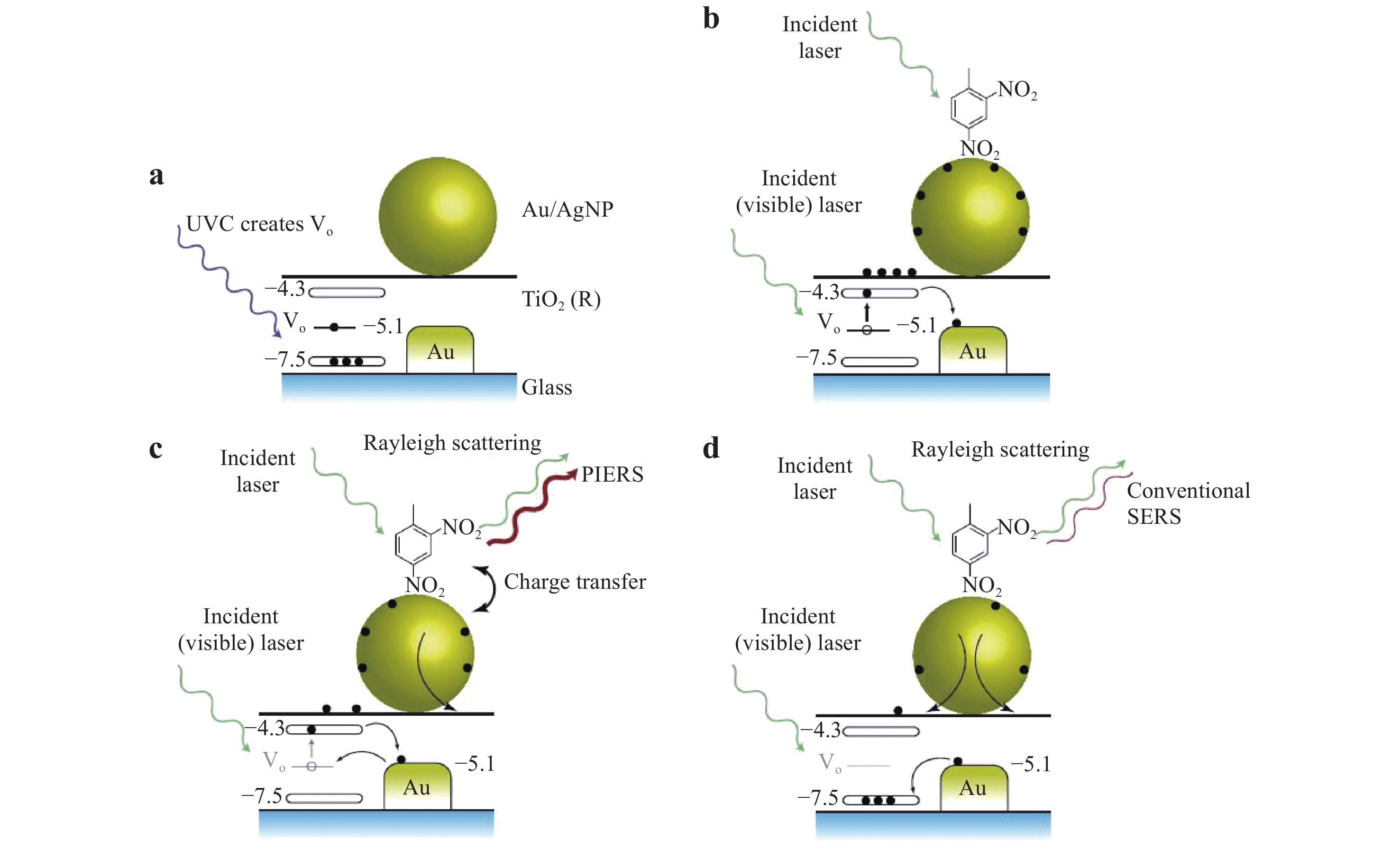
Fig. 9 Enhancement mechanism in PIERS.
including a UV light pre-irradiation to create oxygen vacancies in TiO2, b increased charges on the nanoparticles by Raman laser excitation, c enhanced signals from charged nanoparticles, and d gradual disappearance of the PIERS effect over time (30 – 60 min)103. © 2016 by Author (s).$$ {\rm{\Delta N/N = - 2\Delta \lambda /\lambda }} $$ (16) where λ is the initial wavelength used for the LSPR and Δλ is the wavelength shift due to electron injection. The rate of change of the concentration of the induced Vo states is given by
$$ {\rm{dEff}}{{\rm{V}}_{\rm{o}}}{\rm{/dt = dV}}_{\rm{o}}^ + {\rm{/dt + dV}}_{\rm{o}}^ - {\rm{/dt}} $$ (17) where EffVo is the effective number of Vo states created on the surface; moreover,
${\rm{dV}}_{\rm o}^+ $ /dt and${\rm{dV}}_{\rm o}^- $ /dt represent the rates of vacancy formation and vacancy relaxation, respectively. In addition, owing to the Schottky contact at the semiconductor-metal interface and injected charges, the Fermi level of the metal shifts to a more negative potential, which improves the CT such that it is increased by a factor of 20 when compared to conventional SERS103. -
As noted in Section 1, 3D nanostructured substrates can be employed to obtain highly sensitive SERS analyses because of the significantly higher density of hot spots in such structures. However, it is considerably challenging to fabricate a 3D substrate with sub-100 nm gaps. Additionally, 3D surfaces with sub-100 nm gaps tend to be super-hydrophobic, implying that analyte molecules may not migrate into the nanogaps104. Consequently, the SERS signal intensity obtained from 3D substrates is often inferior to that from 2D substrates. A novel strategy based on transient SERS utilizing droplet evaporation was proposed to address this issue by mitigating the super-hydrophobic effect to achieve femtomolar-level detection. Fig. 10 presents a summary of the transient SERS process. In this technique, the analyte is mixed with metal NPs and a volume of approximately 1 μL is applied to the substrate, after which the Raman excitation laser is focused on the droplet and the Raman scattered light is collected. Initially, a signal is not obtained because the system operates in the ordinary Raman mode (Fig. 10a). As the droplet evaporates, the NPs are immobilized in an ordered 3D structure to produce a hot spot matrix, which boosts the signal intensity (Fig. 10b). It is also important to note that, as the evaporation proceeds and the distance between adjacent NPs becomes smaller than 1 nm, quantum tunneling effects dramatically reduce the electromagnetic enhancement effect and the signal is weakened (Fig. 10c)105.
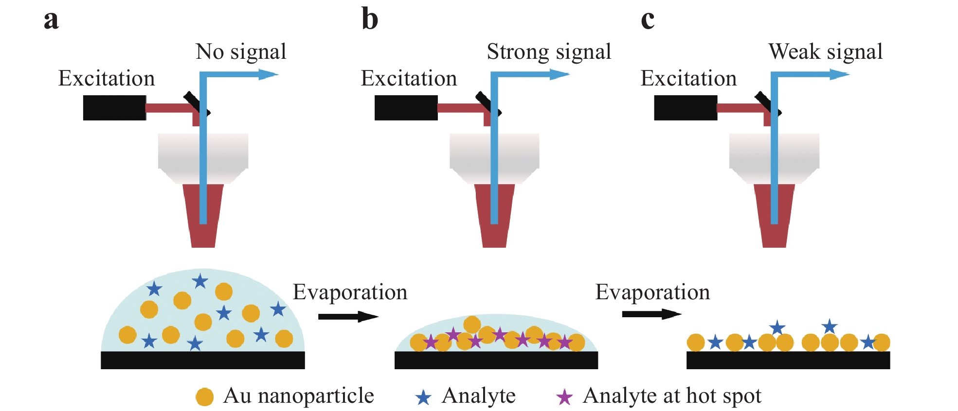
Fig. 10
a Diagram illustrating transient SERS utilizing droplet evaporation, b formation of three-dimensional (3D) hot spots during droplet evaporation, and c collapse after complete evaporation. Modified from Ref.105.Fig. 11 shows the typical results obtained using the transient SERS method106. Initially, the signal slowly increased up to approximately 600 s, after which the signal increase accelerated up to 700 s and plateaued at an extremely high intensity for close to 100 s. The signal subsequently abruptly faded to nearly zero (Fig. 11a). Following the evaporation of the droplets, a highly ordered nanostructure was observed, as shown in Fig. 11b, owing to the self-assembly based on the so-called coffee ring effect28, 107. This densely assembled nanostructure promoted charge exchange, leading to a decay in the electric field enhancement that eventually quenched the SERS effect. Barmi et al. established a model to determine the optimum NP aggregation required to achieve the maximal SERS intensity108. Their model indicated that both the analyte/NP aggregation time and liquid evaporation time are important factors affecting transient SERS. Tuning both the extent of aggregation and the evaporation time can provide a sub-femtomolar detection limit, as shown in Fig. 11c.

Fig. 11
a Variations in the Raman signal intensity from a 10 fM rhodamine 6G (R6G) solution over time using transient SERS106. Reproduced with permission from RSC. © 2015 by Royal Society of Chemistry. b SEM image of the highly ordered Ag nanostructure after solvent evaporation28. Reproduced with permission from RSC. © 2015 by Royal Society of Chemistry Publishing. c Typical transient SERS spectra acquired with various R6G concentrations106. Reproduced with permission from RSC. © 2015 by Royal Society of Chemistry. -
Recently, a novel method termed LI-SERS was reported by Bai et al85. This technique provided attomolar-scale sensing during trials using R6G and crystal violet molecules. Fig. 12a presents a diagram of the LI-SERS setup, in which a microfluidic SERS chip was fabricated by hybrid femtosecond laser processing59. The Raman excitation laser was focused on the SERS substrate in the microfluidic channel such that, as the analyte liquid interface moved through the beam, the Raman scattering was significantly enhanced and the EF was increased to 1014. This achieved an increase in the EF by a factor of 106 when compared to ordinary SERS. The detection limit of this LI-SERS process was as low as 10−17 M, corresponding to attomolar-scale sensing. It has been suggested that the associated mechanism may result from the local aggregation of analyte molecules. This aggregation is evidently induced by the Marangoni effect due to laser heating at the liquid-air interface during the Raman analysis, which forces analyte molecules to enter into hot spots to enhance the signal intensity. In principle, LI-SERS is universal; therefore, the types of material substrates do not significantly impact LI-SERS. However, Raman nonactive materials such as glass are better suited for use in a manner similar to conventional SERS. Meanwhile, the wettability of the substrate may influence the performance of LI-SERS.
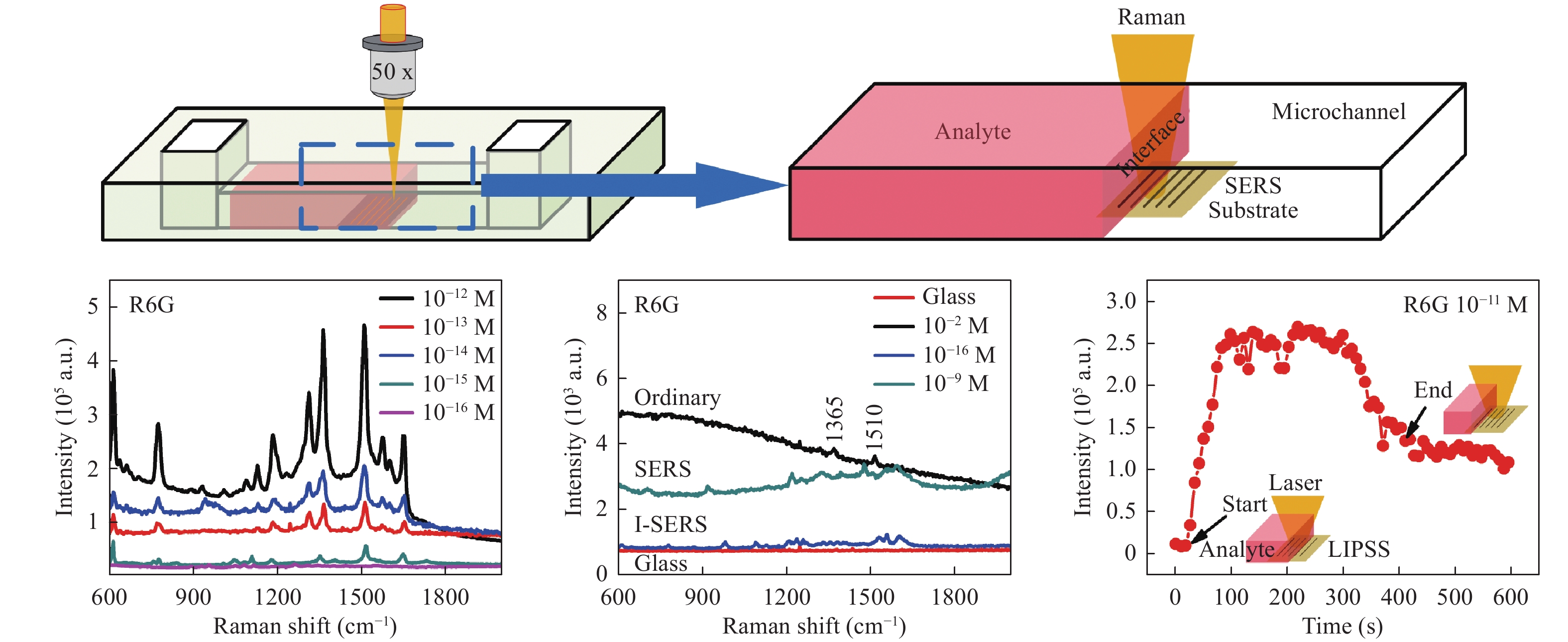
Fig. 12
a Diagram of liquid-interface SERS (LI-SERS) using a microfluidic SERS chip and b LI-SERS results for various concentrations of R6G. c R6G detection limits obtained from ordinary Raman (black), SERS (cyan), and LI-SERS (blue) analyses. The red line is the Raman spectrum for the glass substrate. d Raman signal from a R6G solution over time from a LI-SERS analysis85. © 2020 by Author (s). -
In recent years, certain researchers have explored other strategies to enhance the SERS effect, including pressure-induced109, capillary force25, ribonucleic acid (RNA) technology-combined110, and hydrogel-based techniques111. Sun et al. proposed a pressure-induced SERS method using a MoS2/Au/R6G system109. As shown in Fig. 13a, this system employs two opposing ultralow fluorescence diamond anvils as a cell, with a stainless steel gasket between the anvils. Samples were loaded into the gasket through a drilled hole that was then sealed. Liquid nitrogen was used as a pressure transmitting medium, and the pressure values were determined based on the fluorescence emission from a ruby in the sample chamber. To investigate the effect of high pressure on SERS performance, pressure-dependent SERS spectra were obtained from R6G (Fig. 13b), and it was determined that a pressure of 2.39 GPa significantly enhanced the Raman intensity to achieve an EF as high as approximately 107. Interestingly, the intensity gradually decreased with further increases in pressure. An identical prior work demonstrated that the Raman intensity change was reversible after releasing the pressure. This effect could possibly be due to the pressure-tuned band alignment of the probe molecules and the SERS substrate, which would be expected to favor CT.
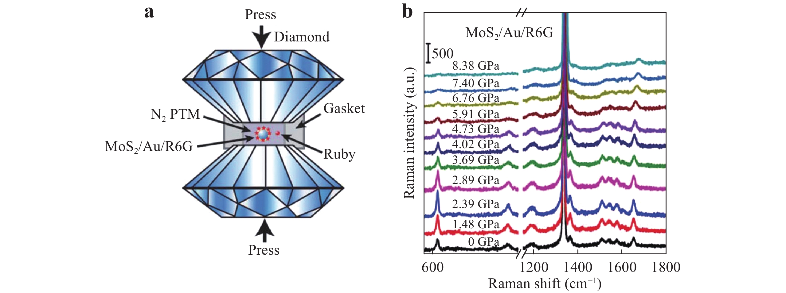
Fig. 13
a Diagram showing a high-pressure experiment with R6G adsorbed on MoS2/Au. b Pressure-induced SERS spectra of this analyte109. Reproduced with permission from RSC. © 2019 by Royal Society of Chemistry Publishing.Combining specific techniques has shown further amplification of the SERS signal. Fig. 14 illustrates an approach in which an electrochemical method is combined with RNA-based nanotechnology to provide a novel technique for SERS sensing of microRNA (miR)110. Briefly, a packaging RNA three-way junction (3WJ) motif was tagged with a Sephadex G-100 resin recognizing RNA aptamer and biotin (SEPapt/3WJ/Bio. Streptavidin-coated AuNPs (STV/AuNPs) were bound to the SEPapt/3WJ/Bio through the streptavidin-biotin interaction (Fig. 14a) and 3WJa functioned as a displacer when the target miR-155 was added (Fig. 14b). Further, the 3WJb-arm was modified to create a multifunctional group and 3WJc was prepared to detect miR, while methylene blue (MB) was fixed at the opposing end of the strand. On applying a potential to the electrode, the STV/AuNP-Bio was pulled down to enhance the SERS signal from the MB (Fig. 14c). As a result of this structural transformation, the SERS signal was significantly increased such that miR could be detected at the attomolar level.
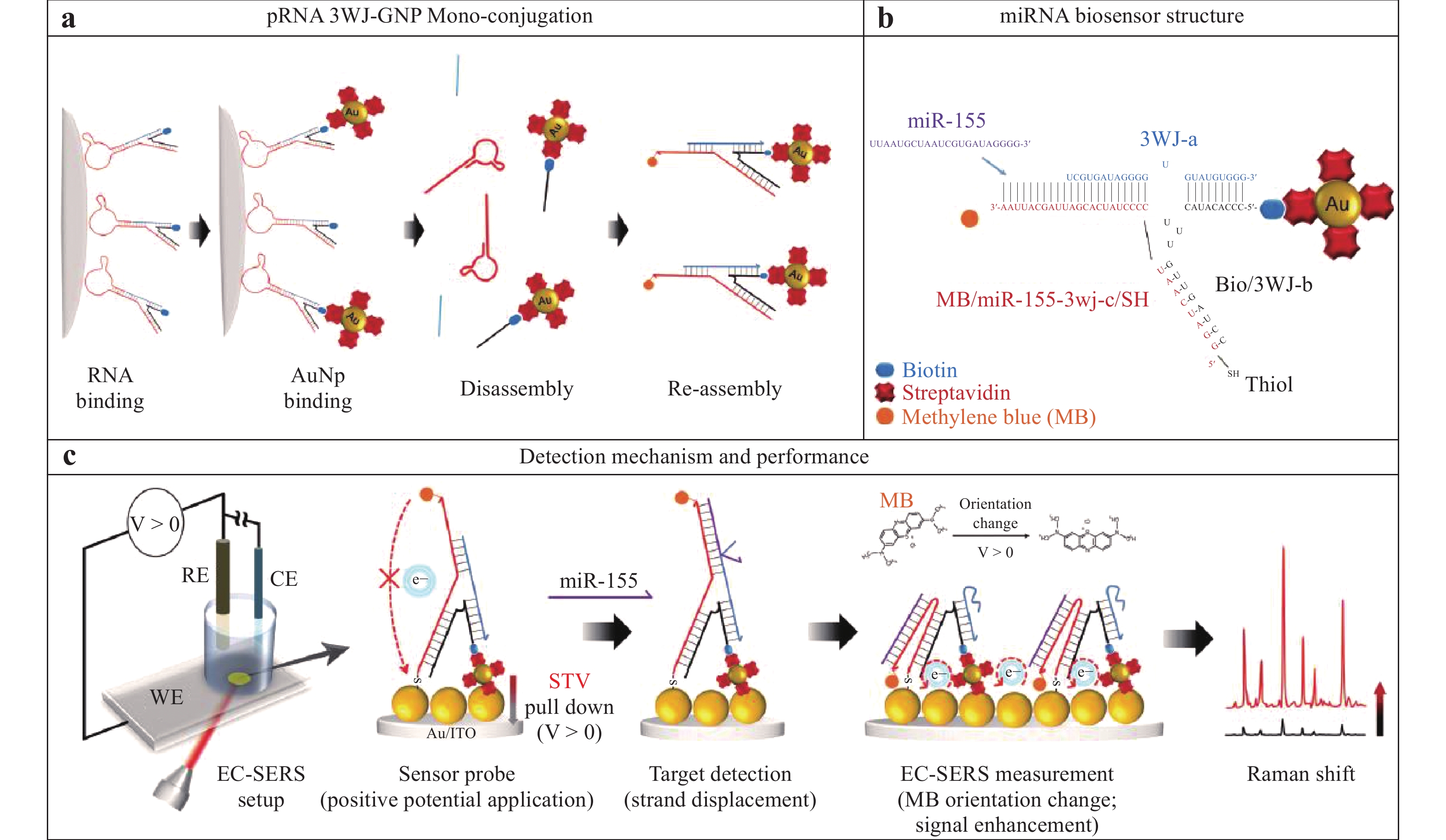
Fig. 14 Diagram showing the monofunctionalization of AuNPs on a ribonucleic acid (RNA) three-way junction structure110.
© 2019 by Author (s). -
In Section 4, we present several recent strategies to enhance SERS intensity including PIERS, transient SERS, and LI-SERS. The synergistic effect is highlighted in these strategies as they explore new pathways to improve the capacity of SERS for attomolar-level sensing. The PIERS method integrates EM and CM of SERS, while the substrate requires pretreatment by light irradiation. Transient SERS provides 3D hotspots, leading to impressive SERS performance. However, the 3D hotspots collapse and vanish during the Raman measurements, showing a transient SERS phenomenon. LI-SERS shows a permanent SERS signal, while the liquid interface is indispensable. A comparison of the detection limit by each strategy is listed in Table 2. These strategies also exhibit potential applications in interdisciplinary fields such as pressure sensing and trace detection of DNA/RNA, which will diversify the practical applications of SERS techniques and exploit SERS products for ultra-trace detection in the near future.
Strategy Analyte Substrate Detection limit Ref. PIERS 4-mercaptobenzoic Ag-doped TiO2 98 PIERS anti-thrombin TiO2@AgNP 50 pM 100 PIERS trinitrotoluene TiO2@AgNP 31 nM 103 Transient SERS CV AuNP 1 nM 105 Transient SERS R6G Ag sol 10 aM 106 Transient SERS R6G Ag sol 500 aM 112 LI-SERS R6G Ag structure 10 aM 85 Pressure-SERS R6G MoS2/Au 100 pM 109 RNA-SERS miRNA RNA/Au 60 aM 110 Electrochemical SERS ascorbic acid Au@Ag 19 nM 113 Electrochemical SERS B12 vitamin Au structure 4.4 nM 114 Table 2. Recent strategies for highly sensitive sensing of surface-enhanced Raman scattering.
Photo-induced enhanced Raman spectroscopy
Transient SERS
Liquid-interface SERS
Other strategies
Comparison of each strategy
-
Because SERS sensing is a versatile, flexible analytical tool that provides high sensitivity, the SERS-based techniques can be applied in diverse fields. In this section, we examine the possibility of real-time sensing using microfluidic SERS chips while providing detailed descriptions of the chip fabrication procedures.
To achieve real-time sensing, the analyte should be continuously supplied to the SERS substrate, and this can be achieved by situating the substrate in a microfluidic chip. In such systems, the analyte flows through a microchannel integrated with the SERS substrate, while the Raman spectra are measured. Microfluidic chips are typically fabricated from polymeric materials (such as polydimethylsiloxane (PDMS), polyvinyl alcohol, or polyethylene terephthalate) or silica glass, and are sealed by bonding with glass or PDMS sheets.
Sun and his group reported a series of studies using femtosecond laser-induced photoreduction to fabricate patterned metal substrates in microfluidic channels63, 74, 115. Fig. 15 presents the process used to obtain the microfluidic SERS chips introduced in Section 3.1. A microfluidic channel is initially fabricated on a glass substrate by wet etching, after which a metal precursor filling the glass microchannel is transferred into the metal nanostructure through two-photon absorption by femtosecond laser direct writing. As shown in Fig. 15a, an 800 nm femtosecond laser is tightly focused on the bottom surface of the glass microchannel to produce a flower-like Ag microstructure. Finally, the glass microfluidic channel is sealed with PDMS for real-time SERS sensing (Fig. 15b). This prior work also demonstrated an Ag/Pd SERS substrate (Fig. 15c) with an extended lifetime owing to the resistance of Pd to oxidation. Because Pd is resistant to aerobic oxidation, the Ag/Pd SERS substrate generated a stable SERS signal for up to 20 days under ambient aerobic conditions63. However, as shown in Fig. 15d, the SERS sensitivity of the Ag/Pd alloy nanostructures decreased notably with increasing Pd content, and deteriorated rapidly at concentrations of 18% or above. The EF values obtained from pure Ag and Ag/Pd (Ag/Pd = 18%) alloy substrates were determined to be 4.04 × 10⁸ and 2.62 × 10⁸, respectively.
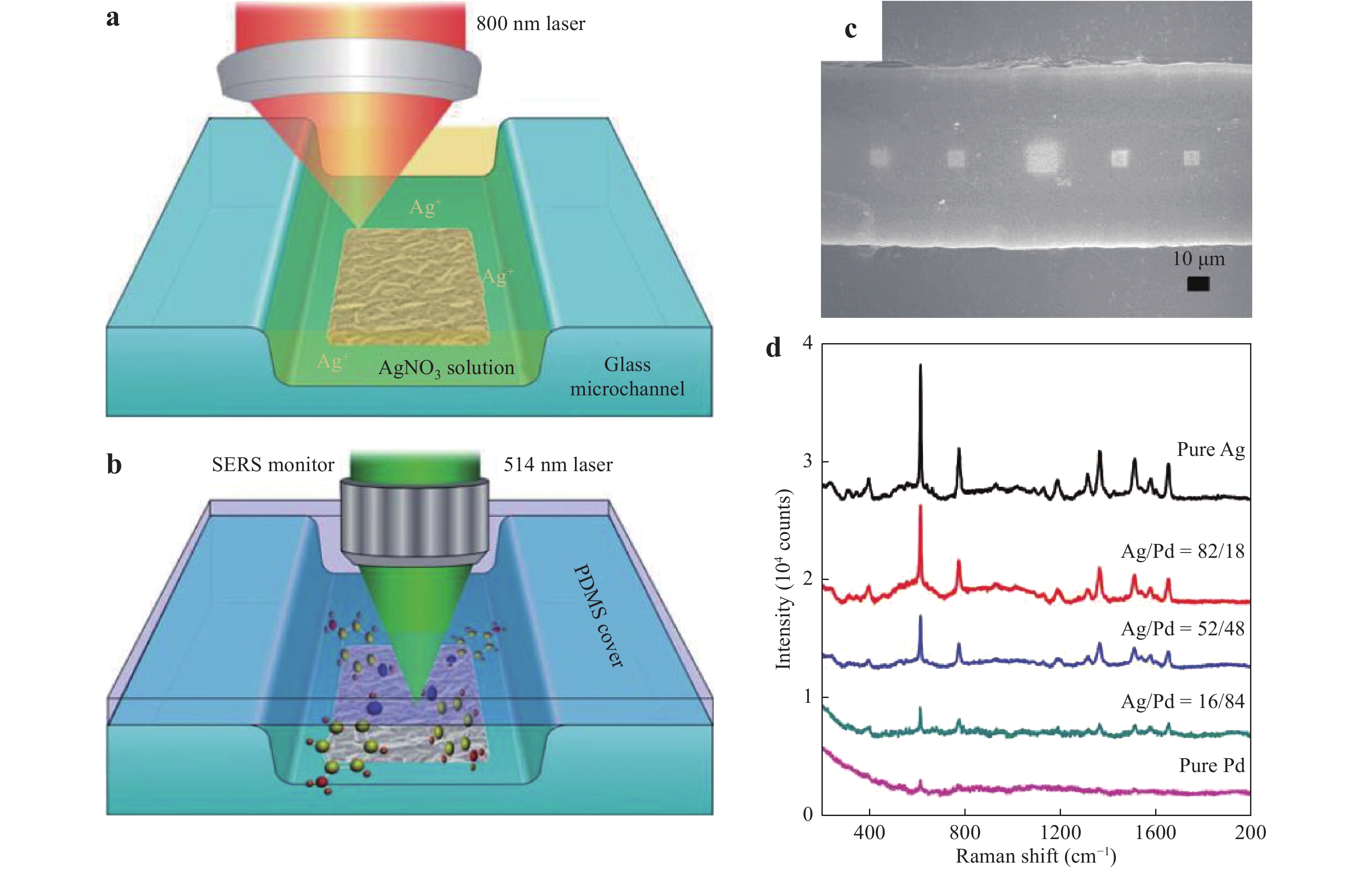
Fig. 15
a Diagram showing the fabrication of a microfluidic SERS chip using the femtosecond laser-induced photoreduction of Ag. b Diagram of a SERS monitor for target molecule detection based on a sealed microfluidic chip74. Reproduced with permission from RSC. © 2011 by Royal Society of Chemistry. c SEM image of a microfluidic SERS chip with an Ag-Pd alloy nanostructure. d SERS spectra obtained from R6G using Ag-Pd alloy nanostructures at different Ag/Pd ratios63. Reproduced with permission from WILEY‐VCH. © 2017 by John Wiley and Sons.AgNPs can be synthesized in a microfluidic channel through photo-induced reduction to permit real-time SERS sensing. Yan et al. observed that two-step irradiation with a femtosecond laser resulted in photoreduction, which enhanced the SERS signal to provide a 0.1 pM detection limit in the channel116. Specifically, AgNPs were first aggregated in the microfluidic channel by femtosecond laser-induced photoreduction. After washing out the precursor, the same laser was applied to the aggregated AgNPs to form numerous small AgNPs on the formerly aggregated NPs and create new hot spots.
Kang et al. used a photoinduction method to fabricate a hybrid Ag/ZnO SERS structure in a microfluidic channel.117 As shown in Fig. 16a, the channel was formed in the PDMS. ZnO nanowires prepared by hydrothermal synthesis on the substrate were coated with AgNPs by a photoinduction process. The microfluidic channel was subsequently sandwiched between the SERS substrate and the cover glass for SERS sensing. This chip was used to detect glucose in real time with a 1 fM detection limit, as demonstrated in Fig. 16b.
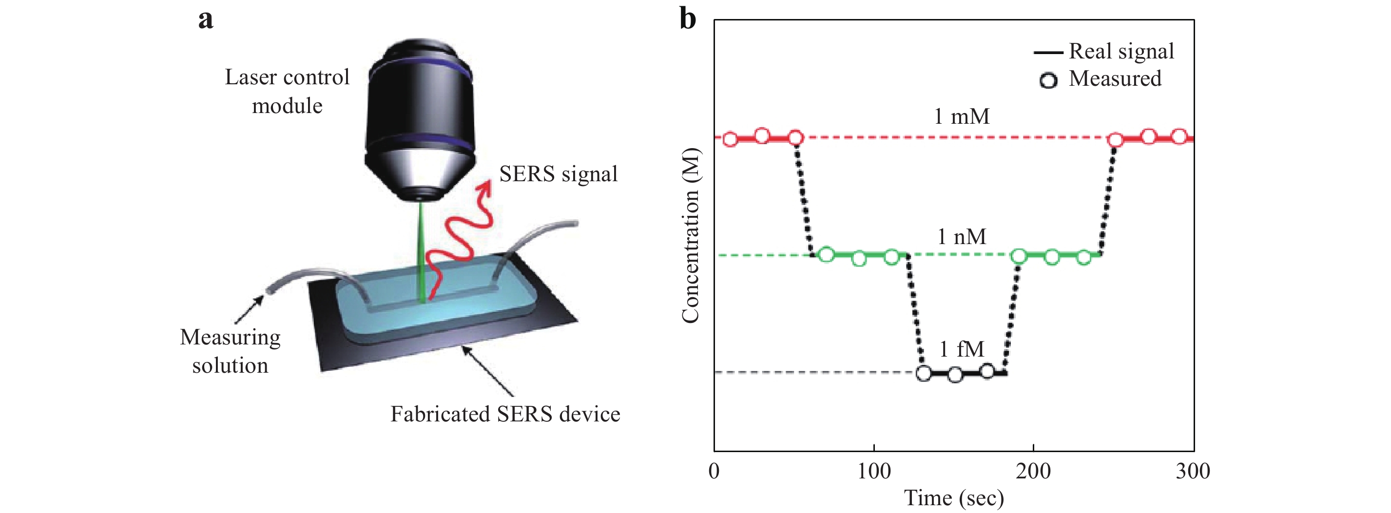
Fig. 16
a Diagram illustrating the assembly of a microfluidic SERS chip integrated with a hybrid Ag/ZnO SERS structure and real-time SERS detection. b Data from the real-time sensing of glucose at varying concentrations over time117. Reproduced with permission from RSC. © 2014 by Royal Society of Chemistry Publishing.Another approach to microfluidic SERS analysis uses metal nanocolloids to analyze a mixture of the analyte and nanocolloids in a channel. In this processes, the analyte and NP colloids are either mixed using a connector before injecting them into the microchannel (Fig. 17)118 or are combined in multi-interconnected microchannels in the chip after injection119. By controlling the flow velocity of the analyte liquid and NP colloids, stable and reliable SERS signals have been generated120, 121. Note that, because the NPs and analyte are expelled after the SERS analysis, the microfluidic chips can be reused.
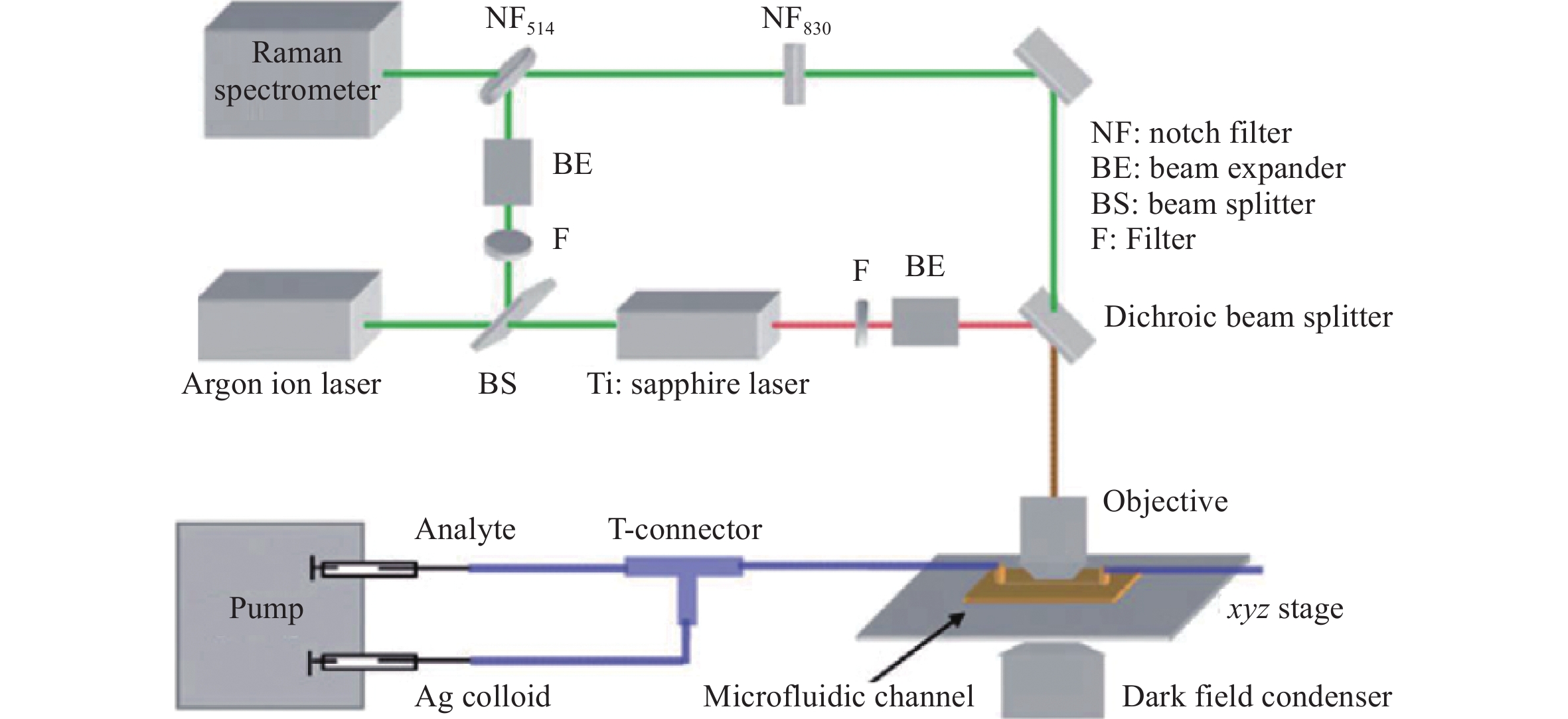
Fig. 17 Diagrams and photographic images of microfluidic SERS chips using metal colloids.
Analyte and metal colloids are mixed in a T-connector before injection into a microchannel118. Reproduced with permission from RSC. © 2008 by Royal Society of Chemistry.Recently, Bai et al. used a 3D glass microfluidic chip instead of polymeric materials (Fig. 18)59. This was advantageous because certain polymers are Raman active, which can be an issue in several applications using portable Raman spectrometers. To overcome this challenge, the Raman signals from the polymer substrates must be carefully removed with a confocal setup. Glass is a considerably more suitable material for microfluidic SERS chips because it generates minimal Raman signals. Fig. 18a shows the procedure used to fabricate a 3D glass microfluidic SERS chip, based on all-femtosecond-laser-processing using a single workstation. In this process, the 3D glass microfluidic structure is first fabricated using femtosecond laser-assisted chemical etching of photosensitive Foturan glass, which is based on femtosecond laser direct writing followed by thermal treatment and successive chemical wet etching70. Subsequently, a metal film is formed on one part of the bottom surface of the microchannel by selective laser metallization; then, ablation by femtosecond laser direct writing is performed, followed by electroless metal plating122. Finally, a periodic nanostructure (that is, an HSFL pattern) is fabricated on the deposited metal film using a linearly polarized femtosecond laser at a laser fluence near the ablation threshold. The resulting microfluidic SERS chip is connected to two micropumps to induce analyte flow through the microchannel. Simultaneously, the SERS signals from the continuous flow of analyte (at varying concentrations) were collected on the chip in real time (Fig. 18c). This microfluidic SERS chip allowed the real-time detection of trace quantities of heavy metal ions such as Cd+ mixed with a dye liquid, with a detection limit as low as 10 ppb.
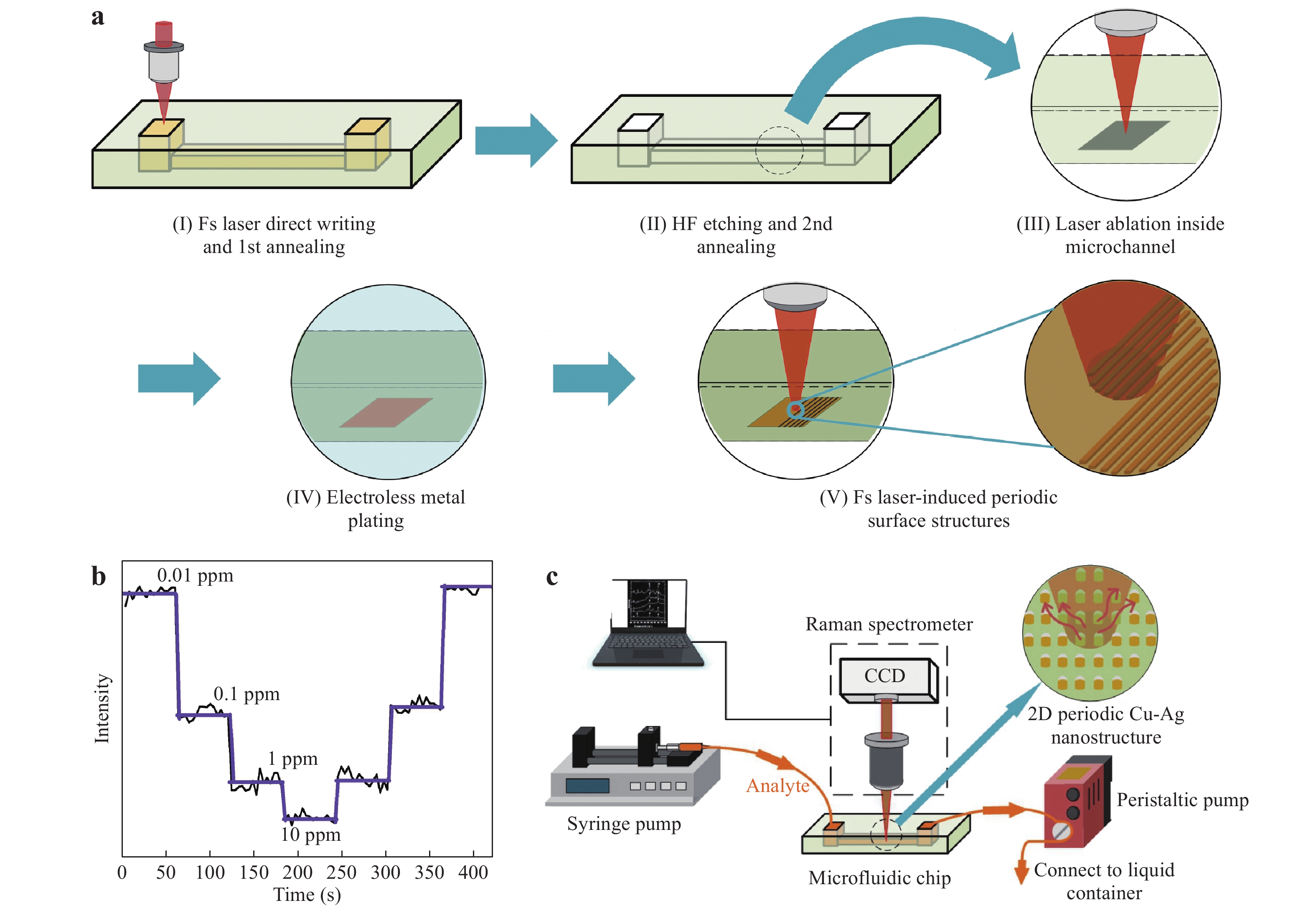
Fig. 18
a Diagram illustrating the fabrication of a 3D glass microfluidic SERS chip by all-femtosecond-laser-processing (Fs: femtosecond; HF: hydrogen fluoride). b Real-time detection of metal ions at various concentrations over time using this chip. c Illustration of the real-time SERS detection system59. Reproduced with permission from WILEY-VCH. © 2018 by John Wiley and Sons.Thus, microfluidic SERS chips can be fabricated using various methods such as femtosecond laser processing and photoreduction. Because of its ability to collect real-time SERS signals using a spectrometer by continuously introducing analytes into the microchannel, as shown in Figs. 18b and 20c, the microfluidic SERS chip is suitable for dynamic measurements such as water quality monitoring, atmospheric monitoring, and identification of cells in a flow. Real-time measurement using microfluidic SERS chips is more reproducible than static conditions because of the more uniform distribution of analyte molecules and the heat dissipation characteristics. Such reproducibility is essential for the quantitative measurements of analytes at low concentrations for practical applications. In particular, the microfluidic SERS chip composed of the embedded microchannel, as shown in Fig. 20, provides a closed circumstance, which can exclude the negative interference by external environments. These advantages have led to the growing interest in the fabrication and applications of microfluidic SERS chips.
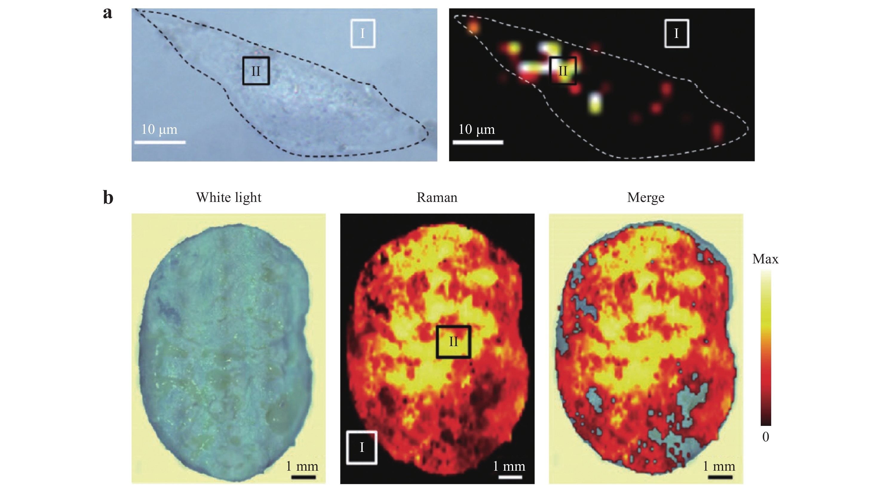
Fig. 20
a Left: optical image of a single MDA-MB-231 cell incubated with hyaluronic acid and 4-aminothiophenol linked to Au nanoframeworks (HA-4-ATP-AuNFs). Right: 2D Raman mapping of the cell. b Left: optical image of excised tumor tissue under white light. Middle: Raman imaging of the tissue. Colors represent intensity of the characteristic Raman band of HA-4-ATP-AuNFs at 1585 cm−1. Right: Merged optical image and Raman mapping123. Reproduced with permission from WILEY-VCH. © 2020 by John Wiley and Sons.
-
The application of SERS in the field of biotechnology has attracted a significant amount of interest because it allows rapid detection and response in non-laboratory environments. One advantage of SERS in terms of bio-applications is the ability to use this method at the point of care to allow targeted detection and therapy46, 123. The majority of SERS research related to biotechnology has focused on the imaging of cells, sequencing of large biomolecules, such as DNA, and cancer cell screening. It is worth noting that the SERS substrates may interact with cells and tissues. Therefore, biocompatibility and cytotoxicity should be considered. Additionally, the stability of the SERS substrate mixed with cells should be considered for achieving reliable and robust SERS results. As this review emphasizes the fabrication and applications of SERS substrates, we do not discuss the influence of SERS on biological systems.
-
In principle, the application of SERS for cell imaging can be considered as an optical labeling technique, and typically uses noble metal NPs for Raman enhancement. In such methods, the metal NPs used as SERS tags have to be tightly held in proximity to Raman reporter molecules. Various biomarkers are stabilized with NPs and taken up by the cells, which are deposited close to the intracellular vesicles, perinuclear locations, and cell membrane. Consequently, cell images can be obtained by Raman mapping based on the SERS tags, providing 2D and 3D morphologies of the cells124. The ability to enhance the SERS signal as well as the cytotoxicity and stability of the SERS tags is essential for obtaining clear images and for allowing quantitative detection of living cells. Therefore, depending on the cell species, the synthesis route to the SERS tags must be carefully considered.
Fig. 19 summarizes the process used to detect miR in a living cell employing side-by-side and end-to-end arrowhead AuNP dimers (AHSBS and AHETE, respectively), as reported by Li et al125. Because the AHETE dimers generated a higher electric field in the head gap owing to the highly concave-convex arrowhead surface, these dimers significantly increased the capacity of the SERS technique to detect miR. Several cell lines were used to demonstrate the quantitative detection of miR, including human breast cancer cells (MCF-7), human cervical cancer cells (HeLa), and primary uterine fibroblasts (PCS-460-010). After incubation of the cells with the AHETE dimers for 8 h, the miR-21 in each cell line was evaluated by acquiring SERS spectra, as shown in Fig. 19b−e show the Raman maps of intracellular miR-21 combined with the AHETE dimers obtained after incubation with MCF-7, HeLa, and PCS-460-010 cells, respectively. The intracellular miR detection limits in the three cell lines were determined to be 0.011, 0.016, and 0.395 amol
${\rm{ng}}_{\rm{RNA}}^{-1} $ , respectively, confirming the exceptional sensitivity of this technique for the analysis of miR in living cells.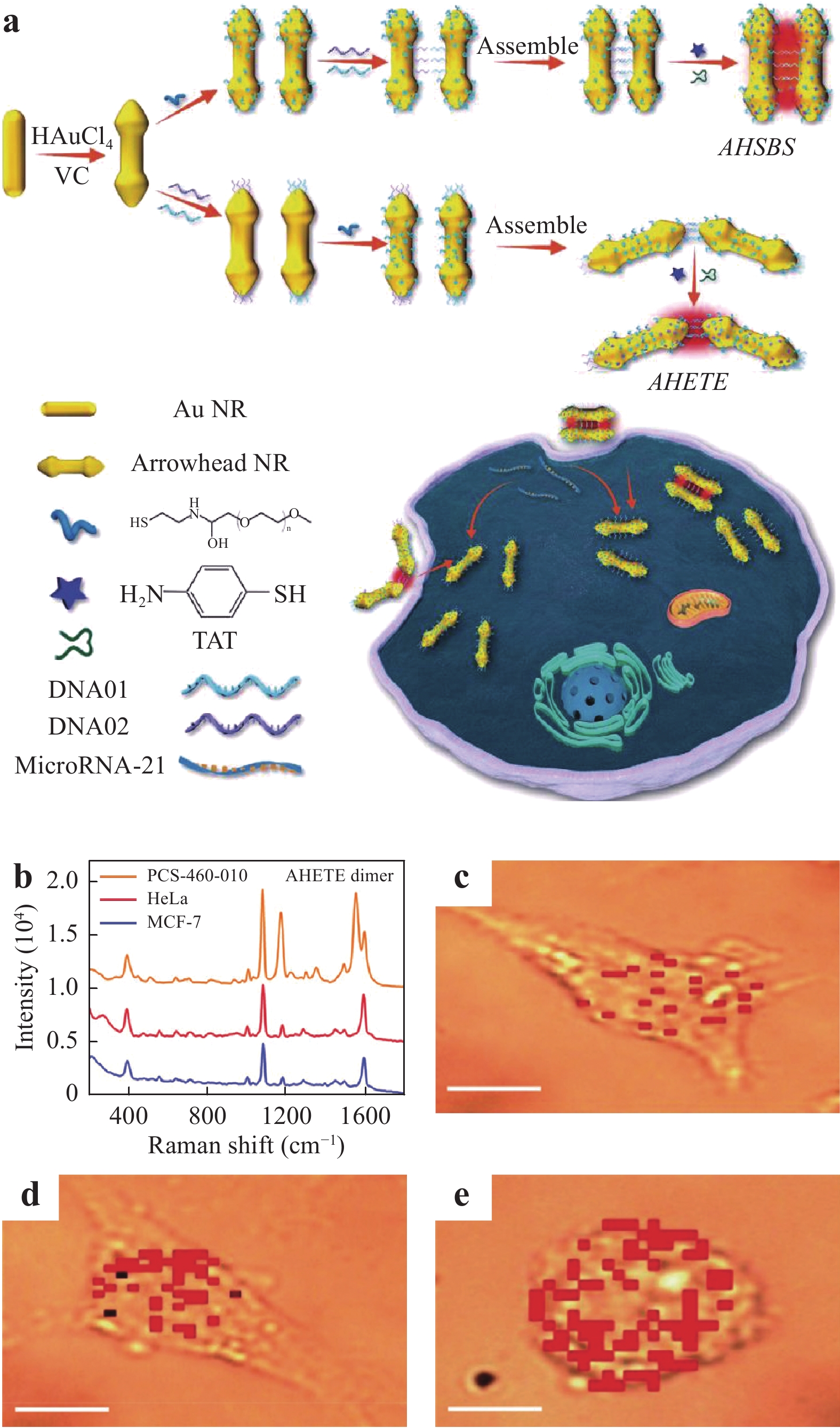
Fig. 19
a Diagram showing the use of deoxyribonucleic acid (DNA)-bridged dimers (side-by-side and end-to-end arrowhead AuNP dimers) to detect microRNA (miR)-21 in living cells. b SERS spectra used to analyze miR-21. c–e Raman images obtained using dimers incubated with human breast cancer cells, human cervical cancer cells, and primary uterine fibroblasts, respectively. Scale bar: 10 μm125. Reproduced with permission from WILEY-VCH. © 2020 by John Wiley and Sons.Wang et al. established an effective theranostic strategy based on SERS imaging123. In their work, SERS tags were made by attaching 4-aminothiophenol (4-ATP, as the Raman reporter) and hyaluronic acid (HA) linked to mesoporous Au nanoframeworks (AuNFs) to create a HA-4-ATP-AuNF system. As shown in Fig. 20a, the resulting SERS maps produced from the strong Raman signals confirmed extensive internalization of the HA-4-ATP-AuNFs and clear cell boundaries. The mesopores in the AuNFs provided an ideal vehicle for drug delivery by offering increased void spaces. After loading doxorubicin onto the AuNFs functionalized with HA, these nanoframeworks were able to bind to targeted tumor cells for therapy, as demonstrated by in vivo SERS imaging that confirmed complete tumor eradication. In addition, 3D SERS images of cells could be obtained by capturing a series of vertical slices using confocal Raman microscopy, and these images allowed exploration of the internal structures of the cells (Fig. 20b)126, 127.
-
To achieve DNA sequencing by SERS, the first challenge is to achieve the capacity for single-molecule detection. It is significantly difficult to identify individual nucleobases in a DNA strand in real time using SERS, because DNA sequencing requires an accurate technique with high spatial resolution and a molecular control method to adsorb the DNA inside hot spots without fluctuations.
Recently, Huang et al. and Chen et al. reported an electro-plasmonic system for the study of DNA in a single hot spot to allow discrimination and sequencing128, 129. Fig. 21 shows a single-molecule trapping setup for DNA discrimination proposed by Huang et al. As shown in Fig. 21a, a SiN membrane was used to form trans and cis compartments, while an Au nanohole with a diameter of 200 nm in a 100 nm thick Au film on this membrane allowed electro-plasmonic trapping. Before trapping, Au nanourchins (AuNUs) were synthesized, on which the nucleotides to be adsorbed were incubated. Because these AuNUs were negatively charged, their behavior could be driven by applying an electric field. Therefore, when the Au nanohole was illuminated with a Raman excitation laser, the AuNUs were dragged to the sidewall by plasmonic force to generate a single hot spot between the AuNUs and the sidewall of the nanohole (Fig. 21b). Consequently, the SERS signal from the nucleobase adsorbed on the AuNUs was enhanced by the gap mode to permit differentiation of the DNA. Monitoring of the variations in the SERS spectra as obtained from the oligonucleotide over time provided information regarding the oligonucleotide conformation.
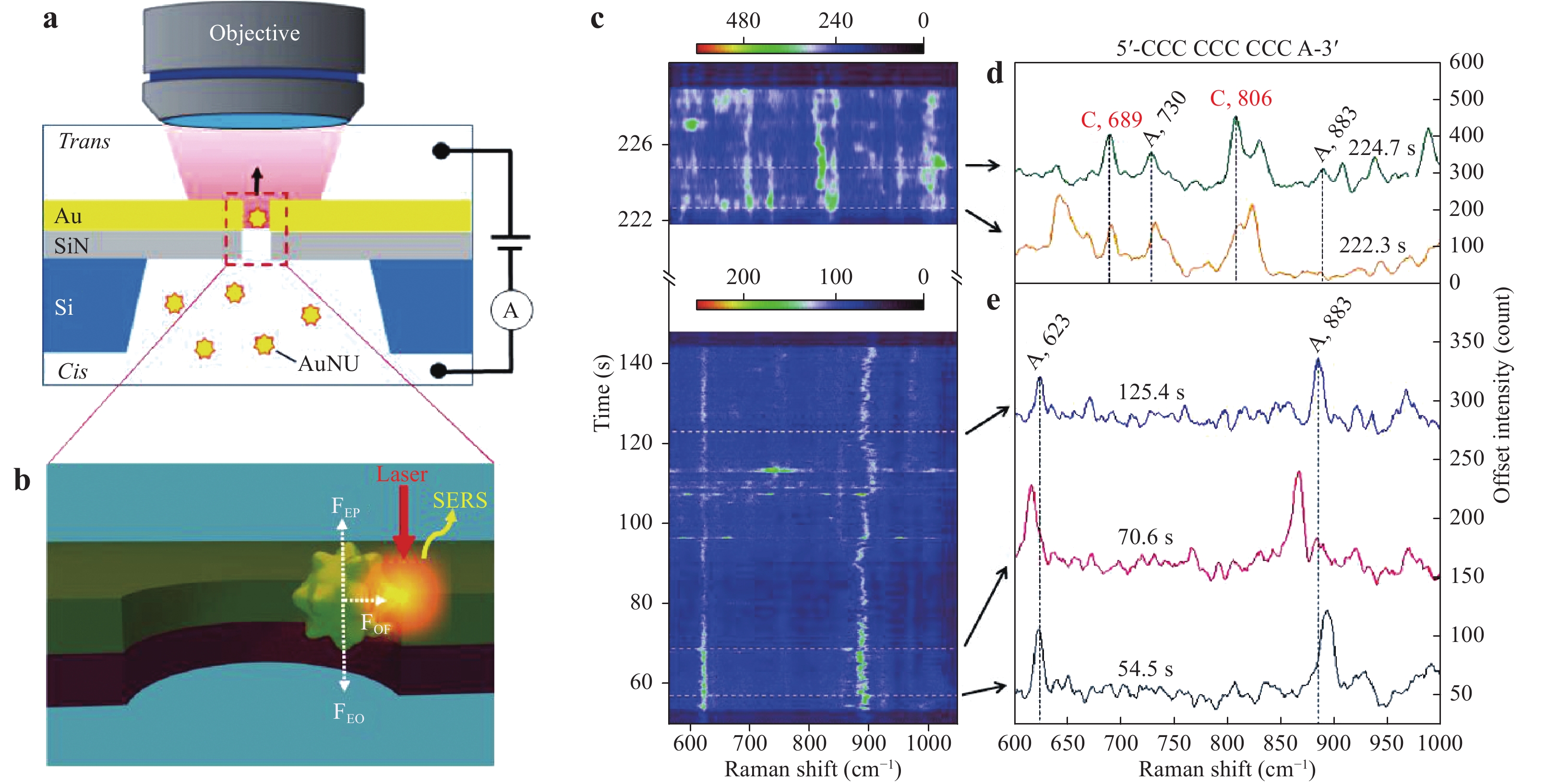
Fig. 21
a Diagram of the single-molecule trapping setup for DNA discrimination. b Diagram showing Au nanourchin trapping to generate a hot spot. c−e SERS discrimination of single nucleobases in single oligonucleotides128. © 2019 by Author (s).Chen et al. used a similar system to perform DNA sequencing. In their work, improved spatial resolution and identification accuracy were obtained by incorporating a nanoslit with a 10 nm neck gap instead of a nanohole, as shown in Fig. 22a–c. As a result of this narrow slit, the stochastic and thermodynamic fluctuations of the DNA strand could be controlled and SERS signals from different DNA bases inside the hot spot could be used to identify adjacent bases (Fig. 22d). Fig. 22e, f present the temporal contour maps obtained from the DNA oligonucleotide sample using this process. A continuous adenine signal was observed, and several transient but asynchronous signals from guanine and cytosine were also evident. This asynchronous blinking behavior indicated the high spatial resolution of nanoslit SERS with regard to DNA sequencing and provided indirect evidence for the ability of this system to identify adjacent DNA bases.
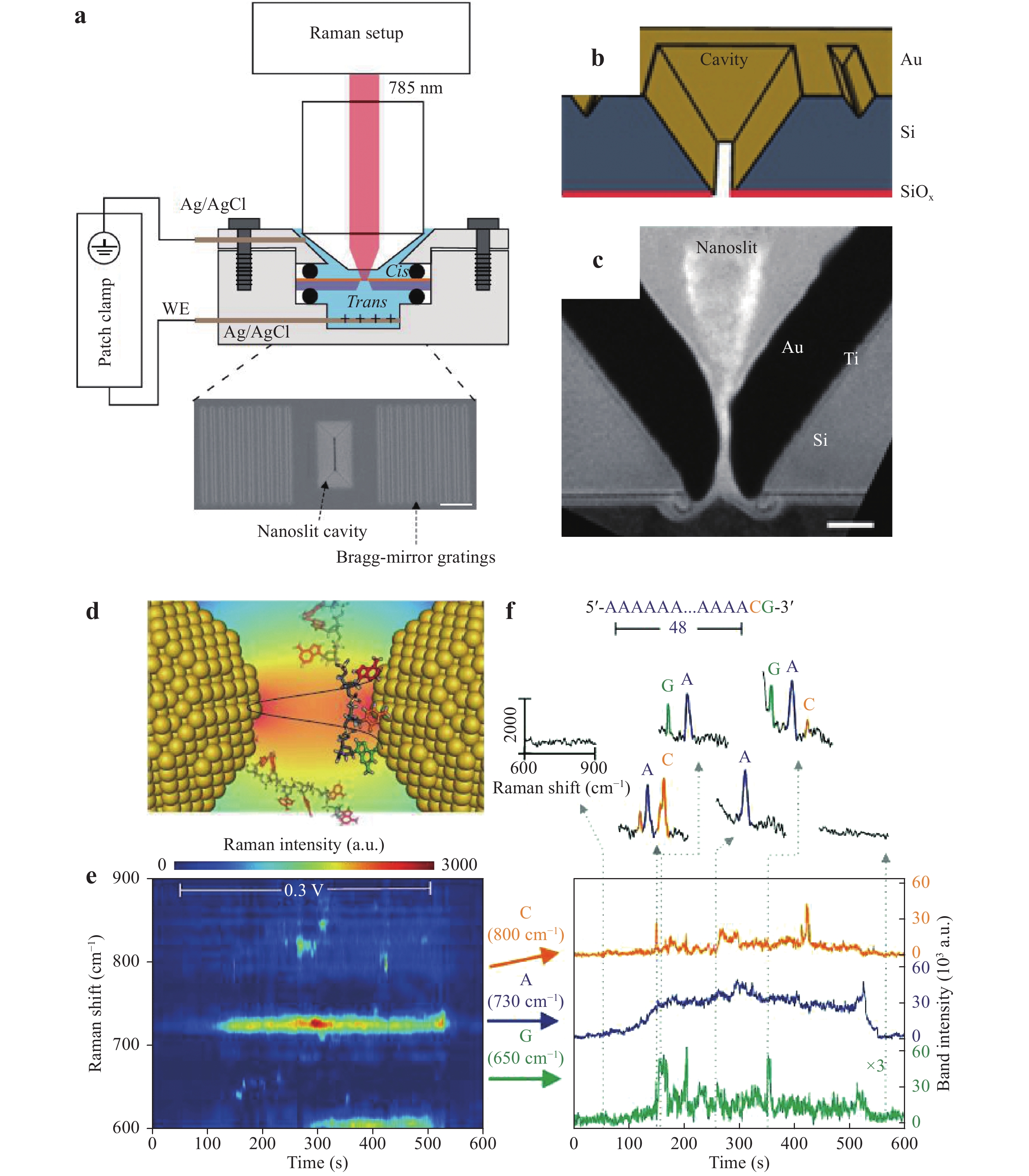
Fig. 22
a−c Diagrams and a photographic image of the setup for nanoslit SERS. d Diagram showing the temporary adsorption of DNA inside the nanoslit. e−f Temporal contour maps obtained from the DNA oligonucleotide sample129. © 2018 by Author (s). -
SERS is also a powerful technique for cancer cell detection and can allow the early diagnosis of diverse cancers because of the strong Raman intensities and narrow spectral bands generated by such cells, which may improve the survival rates of patients130. Cancer cell detection typically involves the selection of the Raman reporter, fabrication of the SERS substrate, selection of the biomarker, preparation of the SERS tags, and analysis of the Raman signal. As shown in Fig. 23, Eom et al. demonstrated a novel SERS sensor for the detection of telomerase activity in breast cancer cells131. This device consisted of nanogap-rich Au nanowires synthesized on a sapphire substrate using a vapor transport method. This substrate was decorated with 30 nm AuNPs using direct-current ion sputtering to generate sub-10 nm nanogaps capable of producing SERS hot spots. Thiolated telomeric substrate (TS) primers were adsorbed onto the SERS sensor through Au-S bonding and elongated to be intercalated by MB (acting as the Raman reporter). Owing to the overexpression of telomerase in cancer cells, the Raman intensity of MB became much stronger than that obtained with healthy cells, which allowed the monitoring of cancer cells at a detection limit of 0.2 cells mL−1. Similarly, Kim et al. fabricated Au-decorated polystyrene nanospheres for the detection of breast cancer cells in human tears20. They identified that the collagen-assigned Raman intensity of the specimens from breast cancer patients was increased by a factor of 3.66 when compared to that obtained from healthy subjects. Zhang et al. used soluble E-cadherin and N-cadherin as biomarkers, and 4-mercaptobenzoic acid as a Raman reporter for the detection of cancer metastasis, and reported a detection limit below 10 cells mL−1 132. Li et al. reported a ratiometric strategy for the detection of breast cancer cells133. Their work demonstrated that, by quantifying the ratio of urokinase plasminogen activation receptors to epidermal growth factor receptors, two breast cancer cell lines (MDA-MB-231 and MCF-7) could be detected. Haldavnekar et al. synthesized a nano-dendrite platform by laser deposition such that ZnO quantum dots were transported into cells by endocytosis for in vivo cell imaging134. When using magnetic plasmonic NPs that were selectively taken up by cancer cells, these cells could be imaged as well as separated from healthy cells based on magnetic attraction135. Combining this process with a microfluidic chip allowed cancer cells to be dynamically detected without incubation136. SERS data have also been assessed using principal component analysis to determine clinical sensitivity and specificity, to increase the accuracy of cancer cell discrimination137, 138. However, the current accuracy and sensitivity of SERS tags for cancer diagnosis are still insufficient for clinical applications. Therefore, it is essential to identify new pathways and strategies for the early diagnosis of cancer.
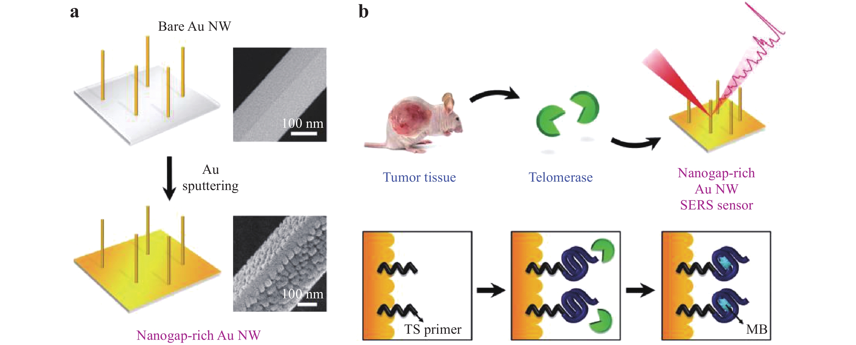
Fig. 23
a Illustration of the fabrication of a nanogap-rich Au nanowire SERS sensor. b Detection of telomerase activity using this type of sensor131. Reproduced with permission from WILEY-VCH. © 2017 by John Wiley and Sons.
SERS tags for cell imaging
Deoxyribonucleic acid sequencing
Cancer cell detection
-
This review summarized the recent developments in the fabrication of highly sensitive SERS substrates. These substrates can provide improved EF values, as reflected by the number of excited analyte molecules or the analyte concentration that can be detected. In addition to low detection limits, new SERS substrates should also be reusable and provide reproducible performance. In particular, we highlighted the fabrication of SERS substrates through femtosecond laser processing. The unique characteristics of femtosecond lasers, such as minimized thermal effect and multiphoton absorption, allow precise processing with a resolution in a sub-100 nm scale. Several representative methods of femtosecond laser processing were illustrated. Multiphoton absorption is beneficial for the fabrication of nanostructures when using metal ion precursors. Owing to the bottom-up fabrication, 3D sophisticated structures can be constructed using layer-by-layer scanning to generate 3D hotspots in a nanostructure, although it is a time-consuming process139. The LIPSS technique is essentially simple and requires no special equipment and environment; thus, it is suitable for time-effective fabrication of a uniform nanostructure array in a relatively wide area. The array of periodic structures fabricated can offer high SERS reproducibility, but this technique provides no 3D fabrication capability. The femtosecond laser-induced nanomelting of nanomaterials is attractive for achieving a single plasmonic nanodevice for remote SERS using nanowires; however, controlling the melting sites is difficult140, 141.
Recent developments in the fabrication of highly sensitive SERS substrates rely on synergistic enhancement effects, including PIERS, electrochemical SERS, and LI-SERS techniques. These strategies could also provide a pathway to elucidate the SERS mechanism. However, several issues are still associated with the overall progress in the development of SERS. Specifically, a universal method for calculating the EF has not yet been fully established, which makes it difficult to directly compare the performance of different SERS substrates. Further, the stability and robustness of SERS substrates are still insufficient, which limits the practical applications of this technique. However, we believe that further effort related to the development of SERS will address these challenges and lead to a diverse range of applications, and that the versatility of femtosecond laser processing will contribute to the fabrication of highly sensitive SERS substrates in the future.
AHETE end-to-end arrowhead Au NP dimers AHSBS side-by-side arrowhead Au NP dimers AgNPs silver nanoparticles AgNWs silver nanowires 4-ATP 4-aminothiophenol CM chemical mechanism 2D two-dimensional 3D three-dimensional DNA deoxyribonucleic acid EF enhancement factor EM electromagnetic mechanism HA hyaluronic acid HeLa human cervical cancer cells HSFL high spatial frequency LIPSS LIPSS laser-induced periodic surface structure LI-SERS liquid-interface SERS LSFL low spatial frequency LIPSS LSPR localized surface plasmon resonance MB methylene blue MCF-7 human breast cancer cells miR microRNA NF notch filter NP nanoparticle NU nanourchin NW nanowire PCS-460-010 primary uterine fibroblasts PDMS polydimethylsiloxane PIERS photo-induced enhanced Raman spectroscopy R6G Rhodamine 6G RNA ribonucleic acid RSD relative standard deviation SEM scanning electron microscopy SEPapt/3WJ/Bio Sephadex G-100 resin recognizing RNA aptamer and biotin SERS surface-enhanced Raman scattering STV/AuNPs streptavidin-coated Au nanoparticles TS thiolated telomeric substrate UV ultraviolet Vo oxygen vacancies 3WJ three-way junction Table . Abbreviations







 DownLoad: