


-
Polarisation manipulation is of great importance in integrated optical systems, particularly when interfacing rotationally symmetric optical fibres with degenerate polarisation states with highly polarisation-sensitive on-chip waveguides. In conventional optical systems, polarisation manipulation usually relies on discrete optical elements, such as polarisation beam splitters (PBSs) or waveplates made from birefringent materials. These devices offer high polarisation extinction ratios (PERs) and low insertion losses over a large spectral range. However, when used in integrated photonic systems, the viability of discrete polarisation-manipulating elements is limited by, for example, the required footprint and the need for high-precision alignment of these elements with respect to on-chip optical circuits1. Alternatively, polarisation-manipulating functionalities can be integrated into waveguide-based planar photonic circuits, exploiting mode-selective directional or multimode interference couplers2–5, polarisation mode converters6,7, waveguide gratings8, waveguide structures with multi-layer cores9,10, or more complicated structures obtained by inverse design techniques11. These devices can be efficiently realised in large quantities but often require special fabrication steps9,10 and are subject to limitations of the device geometry, dictated by conventional layer-by-layer microstructuring through 2D lithography and dry etching. Moreover, polarisation manipulation in on-chip structures often relies on efficient coupling of light to the associated waveguides in the first place. In silicon photonics, grating-based PBSs can be directly integrated into the fibre-chip interface12. However, these structures are subject to limited bandwidth and still rely on the high-precision active alignment of the single-mode fibre (SMF) with respect to the on-chip grating coupler. Recently, 3D-printing based on multiphoton lithography13–15 has been used to build functional micro-optical elements16–24. This not only include micro-lenses16–18,23,24 and so-called photonic wire bonds19,20, but also PBS structures that can be directly printed onto the facets of SMFs and rely on polarisation-sensitive diffraction gratings21 or directional couplers within photonic bandgap structures22. However, although these demonstrations already show the potential of 3D-printing for the fabrication of PBS structures, the split signals are simply emitted into free space without polarisation rotation or coupling to other waveguide-based devices. In addition, the underlying physical effects of these structures fundamentally limit their bandwidths.
In this study, we demonstrated that ultrabroadband 3D-printed waveguide-based PBSs and rotators open an attractive path towards polarisation manipulation in integrated optics. In our structures, polarisation splitting is accomplished through adiabatic Y-branches of geometrically birefringent polymer waveguides with high-aspect-ratio cross-sections and is complemented by polarisation rotation in waveguides that are twisted along the propagation direction. The structures can be directly incorporated into freeform chip-chip and fibre-chip connections19,20, the so-called photonic wire bonds. In our proof-of-concept experiments, we show monolithic structures that are 3D-printed on the facets of SMFs, comprising ultra-broadband PBSs, polarisation rotators (PRs), and mode-field adapters. Our prototypes feature PERs of more than 11 dB in the wavelength range 1270–1620 nm, with vast potential for further improvement. To demonstrate the practical viability of the structures, we used them in a dual-polarisation data transmission experiment, in which we received a dual-polarisation 16-state quadrature amplitude modulation (16QAM) data stream at a symbol rate of 80 GBd and an aggregate data rate of 640 Gbit/s. We found that our 3D-printed PBS did not introduce any measurable optical-signal-to-noise-ratio (OSNR) penalty when compared to a commercially available fibre-coupled PBS. We believe that 3D-printed optical structures for polarisation manipulation can replace costly assemblies of discrete micro-optical elements, thereby paving the way for optical systems with unprecedented compactness and scalability.
-
The basic concepts of 3D-printed PBSs and PRs in integrated optical assemblies are illustrated in Fig. 1. This device connects a rotationally symmetric SMF with degenerate polarisation states to a highly polarisation-sensitive photonic integrated circuit. As an example, we illustrate a dual-polarisation receiver assembly for coherent communications in which data signals in orthogonal polarisation states of the SMF are split and independently detected using a pair of coherent optical receivers (Coh. Rx), which are fed by a joint local oscillator (LO). PBS/PR can be merged with additional 3D freeform waveguide elements, such as mode-field adapters, into a single monolithic structure. This structure can be fabricated in a single exposure step using high-resolution 3D-laser lithography that exploits multiphoton polymerisation in the focus of a pulsed femtosecond laser beam14. Fabricating the structure in situ onto readily positioned devices offers the freedom to adapt the geometry of the 3D-printed structures to the exact positions of the corresponding optical facets, thereby overcoming the need for high-precision mechanical alignment of the fibre with respect to the chip19,20,25,26. The assembly illustrated in Fig. 1 represents only one example of how 3D-printed polarisation-manipulating elements can be used in integrated optics. In general, structures can be printed on a wide range of optical devices, covering applications ranging from optical communications and signal processing27,28 to optical metrology29, imaging30, and quantum optics31.
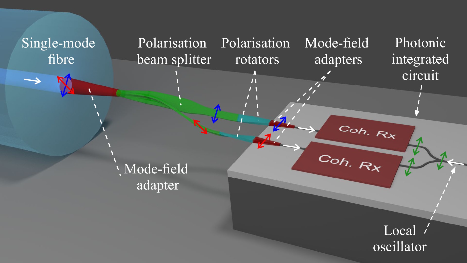
Fig. 1 Concept of a 3D-printed polarisation beam splitter and rotator in an integrated optical assembly (not drawn to scale). The structure connects a rotationally symmetric single-mode fibre (SMF) with degenerate polarisation states (red and blue arrows) to a photonic integrated circuit (PIC) with highly polarisation-sensitive waveguides. As an example of high practical interest, we illustrate a dual-polarisation receiver for coherent communications, in which data signals in orthogonal polarisation states are split and independently detected using a pair of coherent optical receivers (Coh. Rx) which are fed by a joint local oscillator (LO). The polarisation beam splitter (PBS) and the polarisation rotators (PR) can be merged with additional 3D freeform waveguide elements such as mode-field adapters to form a single monolithic structure. This structure can be fabricated in a single exposure step by high-resolution 3D-laser lithography, thereby offering the freedom to adapt the geometry of the 3D-printed structure to the positions of the various optical device facets.
The basic principle of our 3D freeform waveguide-based PBS is illustrated in Fig. 2. Fig. 2a depicts a 3D rendering of an exemplary device implementation, comprising an input waveguide port with a circular cross-section and a pair of output waveguide ports with rectangular cross-sections of a high aspect ratio. As explained in more detail, the separation of orthogonally polarised modes at the input port is accomplished by first transforming the circular cross section at the input port into a cross-shaped cross section formed by the superposition of the two high-aspect-ratio rectangular cross sections of the output waveguides. These initially overlapping partial waveguides are then separated adiabatically, thereby dragging the differently polarised modes to spatially separated output ports. In the following, the input port is denoted by superscript (I), whereas superscripts (H) and (V) refer to the output ports with horizontally and vertically oriented rectangular cross-sections, as shown in Fig. 2a. As an important feature of our PBS, we aimed to ensure identical behaviour of the two output ports H and V, and we therefore designed the PBS to have a geometrically symmetric structure with respect to a mirror plane that contains the axis of the input waveguide and is oriented at an angle of 45° with respect to the horizontally and vertically oriented rectangular waveguide cross-sections in the output plane, see Inset 1 of Fig. 2a. Note that the device is fully bidirectional and can also be used as a polarisation beam combiner, where the two rectangular waveguide ports H and V are used as inputs, whereas the circular port I acts as the output.
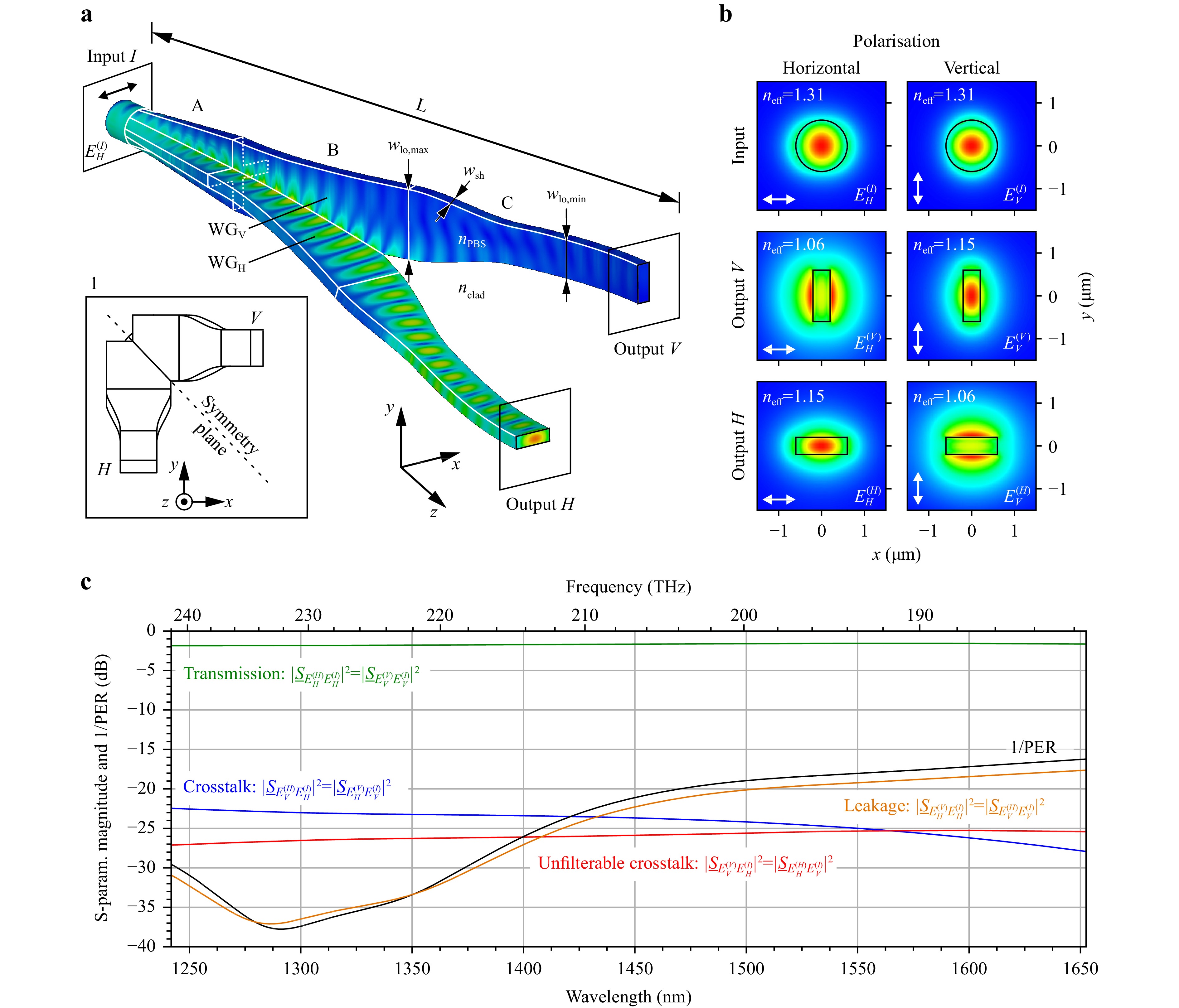
Fig. 2 Concept and design of 3D-printed waveguide-based PBS. a 3D model of the PBS, comprising an input waveguide port with a circular cross section and a pair of output waveguide ports with rectangular cross sections of high aspect ratio. The two orthogonally polarised modes at the input port are denoted as $ {E}_{H}^{\left(I\right)} $ and $ {E}_{V}^{\left(I\right)} $, whereas $ {E}_{H}^{\left(V\right)} $ refers to the horizontally and $ {E}_{V}^{\left(V\right)} $ to the vertically polarised mode at the vertical output V, while $ {E}_{V}^{\left(H\right)} $ denotes the vertically and $ {E}_{H}^{\left(H\right)} $ the horizontally polarised mode at the horizontal output H. The PBS consists of three segments denoted by A, B, and C. Within Segment A, the circular cross section at the input port is adiabatically morphed into a cross-shaped cross section. Within Segment B, the structure can be represented by two spatially overlapping partial waveguides WGH and WGV with high-aspect-ratio rectangular cross sections, which are gradually separated to drag the strongly guided eigenmodes into the two distinct waveguides at the input of Segment C. The 3D rendering of the structure also depicts the simulated electric field distribution for a horizontally polarised excitation $ {E}_{H}^{\left(I\right)} $ at the input port at a wavelength of 1550 nm. The PBS exhibits full geometrical symmetry with respect to a plane that is oriented at 45° between the horizontal and the vertical direction, see Inset 1. The refractive index of the 3D-printed PBS core region amounts to nPBS = 1.53, and the cladding material is air, nclad = 1. b Electric field plots (|E|) of the fundamental modes for both polarisations at all three ports of the PBS, calculated for a wavelength of 1550 nm. The arrows indicate the orientation of the dominant transverse component of the electric field. The strongly guided target modes $ {E}_{H}^{\left(H\right)} $ and $ {E}_{V}^{\left(V\right)} $ at the horizontal and vertical output exhibit a higher effective index and a stronger confinement to the rectangular core than the undesired modes $ {E}_{V}^{\left(H\right)} $ and $ {E}_{H}^{\left(V\right)} $. c Simulated wavelength dependence of the squared magnitudes of complex scattering parameters (S-parameters) and the reciprocal of the polarisation extinction ratio (1/PER) of the PBS on a logarithmic scale. The transmission is better than –2.0 dB with a maximum of approximately –1.55 dB near λ = 1550 nm. The reciprocal of the polarisation extinction ratio (1/PER) and the spurious coupling $\big| $S$ {}_{{E}_{V}^{\left(H\right)}{E}_{H}^{\left(I\right)}}\big|^{2}=\big| $S${}_{{E}_{H}^{\left(V\right)}{E}_{V}^{\left(I\right)}}\big|^{2} $, $\big| $S$ {}_{{E}_{H}^{\left(H\right)}{E}_{V}^{\left(I\right)}}\big|^{2}=\big| $S${}_{{E}_{V}^{\left(V\right)}{E}_{H}^{\left(I\right)}}\big|^{2} $, and $\big| $S${}_{{E}_{H}^{\left(V\right)}{E}_{H}^{\left(I\right)}}\big|^{2}=\big| $S${}_{{E}_{V}^{\left(H\right)}{E}_{V}^{\left(I\right)}}\big|^{2} $ between input and output modes are below –16 dB over the 400 nm wide wavelength range. These parameters can be further reduced for smaller wavelength ranges. Details on how to extract the PER from the simulations can be found in Supplementary Information Section S3.
For a more detailed discussion, we subdivide the PBS into three segments, denoted by A, B, and C, where Segment A is directly adjacent to the input port. Owing to its circular cross section, the input port has two degenerate fundamental modes of orthogonal polarisations with identical effective refractive indices neff. Without loss of generality, we select two basis modes at the input with the dominant transverse component of the electric field aligned in the vertical and horizontal directions, as defined by the two output ports, and denote them as $ {E}_{H}^{\left(I\right)} $ and $ {E}_{V}^{\left(I\right)} $ respectively, as shown in the first row of Fig. 2b for the associated mode-field distributions. Within Segment A, the circular cross section at the input port is adiabatically morphed into a cross-shaped cross section at the transition to Segment B. At this transition, the waveguide can be represented by two spatially overlapping partial waveguides, WGH and WGV with high-aspect-ratio rectangular cross-sections. Owing to the adiabatic transition from a circular cross section to a cross-shaped one in Segment A, the two degenerate basis modes, denoted as $ {E}_{H}^{\left(I\right)} $ and $ {E}_{V}^{\left(I\right)} $ are transformed into the strongly guided modes of these rectangular partial waveguides. In this context, the term ‘strongly guided’ denotes the mode of a rectangular waveguide with its dominant transverse electric field component polarised along the long side of the rectangle. This mode exhibits a higher effective refractive index than its weakly guided counterpart, which is polarised along the short side of the rectangular waveguide core. In Segment B, partial waveguides WGH and WGV are gradually separated, dragging the corresponding strongly guided eigenmodes into two distinct waveguides at the input of Segment C.
Within Segment C, the two distinct output waveguides can be adiabatically tapered and bent to suppress unwanted higher-order modes and route the waveguides to the two output ports V and H. Furthermore, 3D-printed freeform waveguide structures can be directly connected to these output ports, for example, for polarisation rotation, see Fig. 1. The second and third rows of Fig. 2b show various mode-field profiles at the output, where $ {E}_{H}^{\left(V\right)} $ refers to the horizontally and $ {E}_{V}^{\left(V\right)} $ to the vertically polarised modes at the vertical output V, whereas $ {E}_{V}^{\left(H\right)} $denotes the vertically and $ {E}_{H}^{\left(H\right)} $ the horizontally polarised mode at the horizontal output H. In an ideal device, the powers of the degenerate $ {E}_{H}^{\left(I\right)} $ and $ {E}_{V}^{\left(I\right)} $ modes are completely coupled to the strongly guided modes $ {E}_{H}^{\left(H\right)} $ and $ {E}_{V}^{\left(V\right)} $, whereas the weakly guided modes $ {E}_{H}^{\left(V\right)} $ and $ {E}_{V}^{\left(H\right)} $are not excited.
The exact dimensions of the PBS structure shown in Fig. 2a were finally obtained from the numerical simulations. For good performance, the aspect ratio of the rectangular cross-sections of the partial waveguides in Section B should be as high as possible while maintaining compatibility with the resolution of the 3D printing system. In the simulated structure, the short side of the rectangular cross section was chosen to be $ {w}_{\mathrm{s}\mathrm{h}}=400\;\mathrm{n}\mathrm{m} $ based on the resolution of the underling lithography system, see Materials and Methods, whereas the long side varies in the range $ {w}_{\mathrm{l}\mathrm{o}}=$1.2−2.2 µm along the propagation direction. The exact shapes and lengths of the various waveguide sections were obtained by numerical optimisation, where the main goals were to maximise the transmission and PER while keeping the overall PBS structure as small as possible. During this optimisation, we designed the exact trajectories of various freeform waveguides, the trajectories of which were modelled using kink-free B-splines. The resulting length of the structure including all three segments amounts to $ L=21\; {\text {µm}} $. The overall design is reasonably robust with respect to variations in various geometric parameters, thus rendering the PBS concept amenable to high-throughput mass production by in situ laser printing (see Supplementary Information, Section S6).
In Fig. 2a, we illustrate the magnitude of the E-field within the device for operation at a wavelength of 1550 nm for horizontal polarisation at the input. The E-field distribution for vertical input polarisation is obtained by reflection about the symmetry plane. To describe the coupling between various modes at the input and output ports, we used the complex-valued scattering parameters (S-parameters) SIJ. In this description, SIJ refers to the amplitude transmission from $ J $ to $ I $ where $ I,J\in \left\{{E}_{H}^{\left(I\right)},{E}_{V}^{\left(I\right)},{E}_{H}^{\left(H\right)},{E}_{V}^{\left(H\right)},{E}_{H}^{\left(V\right)},{E}_{V}^{\left(V\right)}\right\} $ denote the various modes at the ports of the device. The results for the various simulated power-coupling coefficients, which are obtained by squaring the magnitudes of the corresponding S-parameters, are shown in Fig. 2c. Evaluating the power transmission $\big| $S${}_{{E}_{H}^{\left(H\right)}{E}_{H}^{\left(I\right)}}\big|^{2}=\big|$S${}_{{E}_{V}^{\left(V\right)}{E}_{V}^{\left(I\right)}}\big|^{2} $ from the input to the desired mode of the respective output port, we find an insertion loss of less than 2 dB over the entire wavelength range between 1250 nm and 1650 nm, with a minimum of 1.55 dB near 1550 nm, see green line in Fig. 2c. For each polarisation at the input port, we further extract the power that is coupled to the undesired mode at the corresponding ‘correct’ output port, which is quantified by the crosstalk $\big| $S$ {}_{{E}_{V}^{\left(H\right)}{E}_{H}^{\left(I\right)}}\big|^{2}=\big| $S${}_{{E}_{H}^{\left(V\right)}{E}_{V}^{\left(I\right)}}\big|^{2} $ and which is below –22 dB throughout the simulated wavelength range, see blue line in Fig. 2c. This crosstalk can be suppressed by subsequent polarisation filtering. We further calculate the power coupled to the desired output modes $ {E}_{H}^{\left(H\right)} $ and $ {E}_{V}^{\left(V\right)} $ from the ‘incorrect’ input modes $ {E}_{V}^{\left(I\right)} $ and $ {E}_{H}^{\left(I\right)} $, respectively, which cannot be suppressed by subsequent polarisation filters. This unfilterable crosstalk, $\big| $S${}_{{E}_{H}^{\left(H\right)}{E}_{V}^{\left(I\right)}}\big|^{2}=\big| $S${}_{{E}_{V}^{\left(V\right)}{E}_{H}^{\left(I\right)}}\big|^{2} $ is represented by the red line in Fig. 2c and is below –25 dB throughout the 400 nm-wide wavelength range of interest. We also extract the polarisation leakage $\big| $S${}_{{E}_{H}^{\left(V\right)}{E}_{H}^{\left(I\right)}}\big|^{2}=\big| $S${}_{{E}_{V}^{\left(H\right)}{E}_{V}^{\left(I\right)}}\big|^{2} $, which quantifies the power coupled to the undesired polarisation at the ‘incorrect’ output port for a given polarisation at the input port, thus maintaining its polarisation direction. For our structure, the polarisation leakage is below –17 dB throughout the simulated wavelength range, see orange line in Fig. 2c, and can be further suppressed by subsequent polarisation filters. Finally, we extracted the PER, that is, the ratio of the maximum and minimum powers observed in both modes of an output port when varying the excitation at the input over all possible polarisation states. For each output port, the PER can be obtained from the singular-value decomposition of the corresponding Jones matrix (see Supplementary Information Section S3 for details). We found that the PER was better than 16 dB within the investigated wavelength range and showed a strong increase towards longer wavelengths. Note that the PER and polarisation leakage are better than 30 dB over the wavelength range of 1250–1365 nm, and that this high-performance wavelength range can be shifted by adapting the design of the structure. Note also that, for practical applications, 3D-printed waveguides commonly need to be overclad by an additional material that may serve as mechanical support and environmental protection. However, the presence of the cladding material might require some design adaptations to deal with the associated changes in the refractive index contrast (see Supplementary Section S1), which also includes a more detailed discussion on the fabrication tolerances and robustness of the PBS and the PBS and PR designs in the presence of process variations.
-
To experimentally prove the viability of our concept, we fabricated a series of 3D-printed PBS that are directly connected to the cores of SMFs. We characterise the performance of these devices and use them as part of a receiver in a polarisation-division multiplexing (PDM) data transmission experiment.
In the first experiment, we fabricated a series of free-standing PBS on the facets of an SMF array and measured their performance using an infra-red (IR)-sensitive microscope IR microscope), see Fig. 3a. To ensure low-loss coupling to the SMF core, the structures were equipped with adiabatic mode-field adapters attached to Segment A of the PBS. A scanning electron microscope (SEM) image of the PBS and the mode-field adapter is shown in Fig. 3b. Light was fed to the SMF by a laser emitting at a wavelength of $ \lambda =1510\;{\rm{nm}} $, and a subsequent polarisation controller. At the two PBS outputs, light was radiated into free space and detected by an IR microscope. The centres of the white circles in the images in Fig. 3c match the centres of the corresponding PBS output ports, and the areas of the circles denote the areas that were considered in calculating the corresponding power levels. In the first set of measurements, we showed that the radiated light could be switched between the two output ports of the PBS by varying the polarisation at the input, see Column 1 of Fig. 3c. Specifically, Subfigures 1.1 and 2.1 refer to the cases where the polarisation controller was adjusted for maximum radiation from output ports V and H, with vertically and horizontally oriented waveguide cross-sections, respectively.
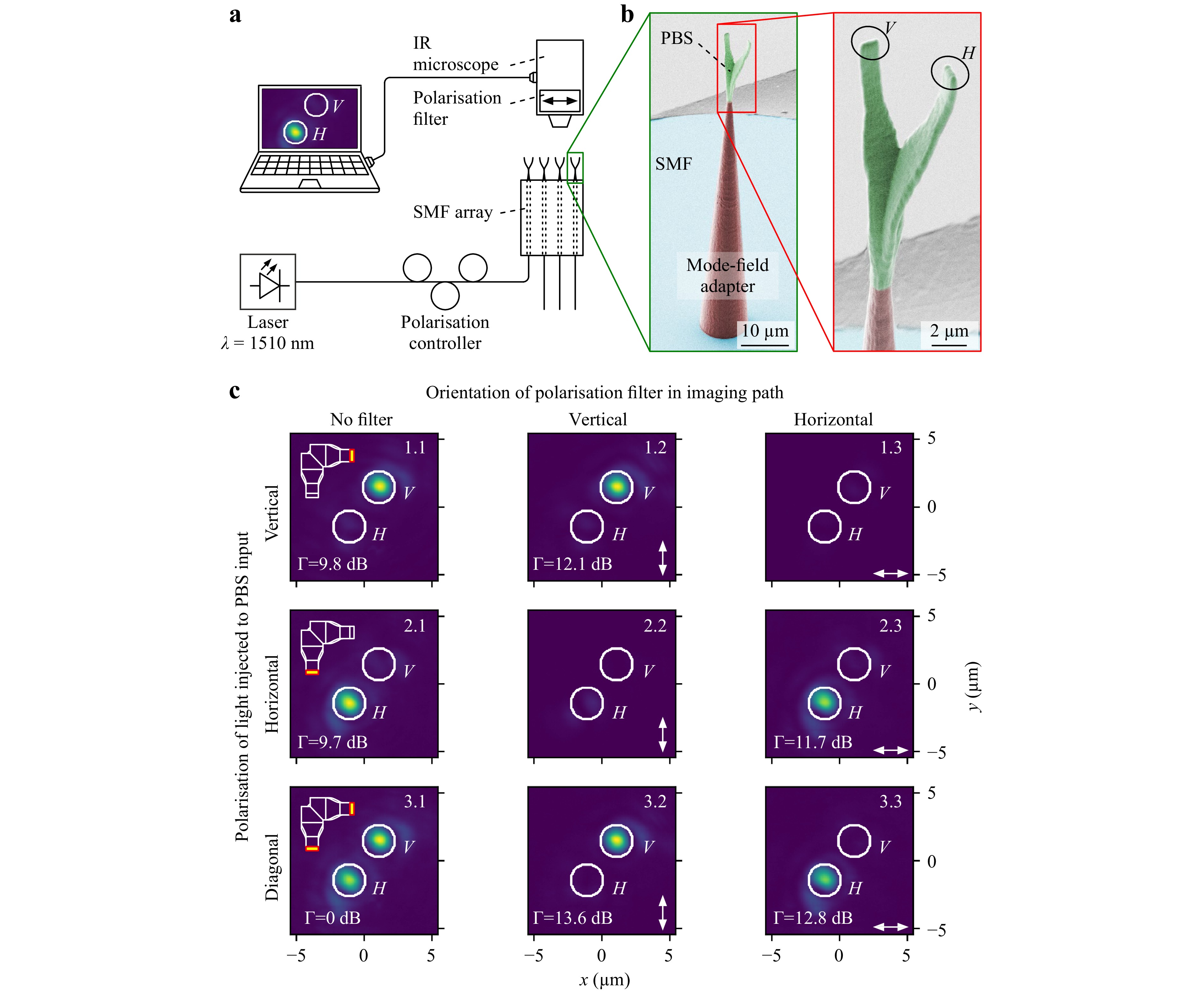
Fig. 3 Characterisation of 3D-printed PBS using an infra-red (IR)-sensitive microscope. a Experimental setup: As test structures, we use a series of PBS that are 3D-printed on the facets of a single-mode fibre (SMF) array. Light at a wavelength of 1510 nm is fed to the devices by a laser and a subsequent polarisation controller. Light emitted from the PBS is characterised by an IR microscope equipped with polarisation filter (PF). b Scanning-electron microscope (SEM) images of a fabricated structure on the fibre array. A linear taper structure, shaded in red, is used at the input of the PBS to adapt the mode-field diameter of the SMF to the one of the PBS input. Within the PBS, which is shaded in green, the light is split into two orthogonal polarisations and emitted from the outputs (V and H) towards the IR microscope. Colours were added by image processing. c Recordings on the IR microscope for different combinations of input polarisation states, indicated by the different rows: Row 1 – vertical input polarisation only, Row 2 – horizontal input polarisation only, and Row 3 – both vertical and horizontal input polarisations. The columns correspond to the measurement of the radiated power without (Column 1) and with vertically and horizontally oriented polarisation filter (Columns 2 and 3, respectively) in the imaging path of the IR microscope. The output power of each port is estimated by integrating the measured intensity over the areas within the white circles, and a power ratio $ \Gamma $ in dB is calculated by dividing the larger by the smaller power. A top view of the PBS structure and the respective ‘active’ output port for each row is additionally illustrated in Column 1. The orientation of the polarisation axis of the PF is illustrated by the double arrows in the lower right-hand corner of the displays in Columns 2 and 3.
In both cases, we measured the ratio $ \Gamma $ of the optical power at the targeted output port to the residual power emitted at the respective other output port, which amounts to 9.8 dB and 9.7 dB, respectively. We also adjusted the input polarisation to yield equal power at both ports, see Subfigure 3.1 in Fig. 3c. To check the polarisation states of the light radiated from the two outputs, we repeated the experiment with a vertically and horizontally oriented polarisation filter (PF) between the microscope objective and the IR camera, as shown in Columns 2 and 3 of Fig. 3c. The PF has an extinction ratio greater than 34 dB. Assuming an excitation with pure vertical polarisation in Row 1 of Fig. 3c, the vertically oriented PF in Subfigure 1.2 suppresses the spurious horizontal polarisation at Port V, which corresponds to the crosstalk S${}_{{E}_{H}^{\left(V\right)}{E}_{V}^{\left(I\right)}}$, and the spurious horizontal polarisation at Port H, which represents the unfilterable crosstalk S${}_{{E}_{H}^{\left(H\right)}{E}_{V}^{\left(I\right)}} $. The measured power ratio $ \Gamma $ of the emitted light after the PF amounts to 12.1 dB and corresponds to the ratio $\big| $S$ {}_{{E}_{V}^{\left(V\right)}{E}_{V}^{\left(I\right)}}\big|^{2}\big/\big| $S${}_{{E}_{V}^{\left(H\right)}{E}_{V}^{\left(I\right)}}\big|^{2} $ of the power transmission at Port V and the leakage at Port H. The measured ratio is smaller than approximately 18 dB expected from the simulation results, see Fig. 2c. We attribute these deviations to the geometrical inaccuracies of the fabricated structures. In Subfigure 2.2, the polarisation controller is adjusted for the maximum radiation from output H, but the PF is oriented vertically such that only spurious horizontal polarisations at both outputs, $\big| $S${}_{{E}_{H}^{\left(H\right)}{E}_{V}^{\left(I\right)}}\big|^{2} $ and $\big| $S${}_{{E}_{H}^{\left(V\right)}{E}_{V}^{\left(I\right)}}\big|^{2} $ can be seen on the IR camera. As expected, the camera image does not exhibit significant power. In Subfigure 3.2, where light exits both the output arms of the PBS, the light radiated from Port H is completely suppressed by the vertically oriented PF, whereas the light radiated from Port V does not experience significant attenuation. The same experiment was repeated with a horizontally oriented PF, see Column 3 of Fig. 3c, thereby reproducing the findings described for the data in the second column. This simple experiment demonstrated that the device works qualitatively as expected.
In the second experiment, we tested our PBS structures by measuring the PER over a broad range of wavelengths. To this end, the polarisation at the input of the structure was varied randomly using a polarisation scrambler, while the Stokes vector and power at the device output were continuously recorded using a polarimeter (see Supplementary Information Sections S2–S4). The measurement was repeated for each output port to reveal the output polarisation state of the maximum and minimum power transmissions as well as the associated PER. The PBS test structure used in this experiment was again 3D-printed on the facet of an SMF array connected to a polarisation scrambler. At the output, the structure was equipped with a pair of PRs realised by rectangular waveguides twisted along the propagation direction32,33. Twisting one waveguide by +45° and the other by –45° thus leads to identical polarisations at both output ports, see Fig. 1 and Fig. 4a. For better probing of the output, the structure was equipped with adiabatic mode field adapters held by a table-like mechanical support structure, as shown in Fig. 4a. Hence, the output ports can be individually read out by an SMF (see Supplementary Information, Section S2, for details on the experiment). We obtained a measured PER better than 11 dB in the wavelength range of 1270–1620 nm, which was limited by the tuning range of the underlying laser sources (see Fig. 4b). The measured insertion losses at 1550 nm for Output I and Output II correspond to 4.4 dB and 3.8 dB, respectively, including the loss of the PBS, of the subsequent PR, and of the adiabatic mode-field adapters see Fig. 2c. A more detailed comparison of the measurement results and simulations is provided in Supplementary Information, Section S2.
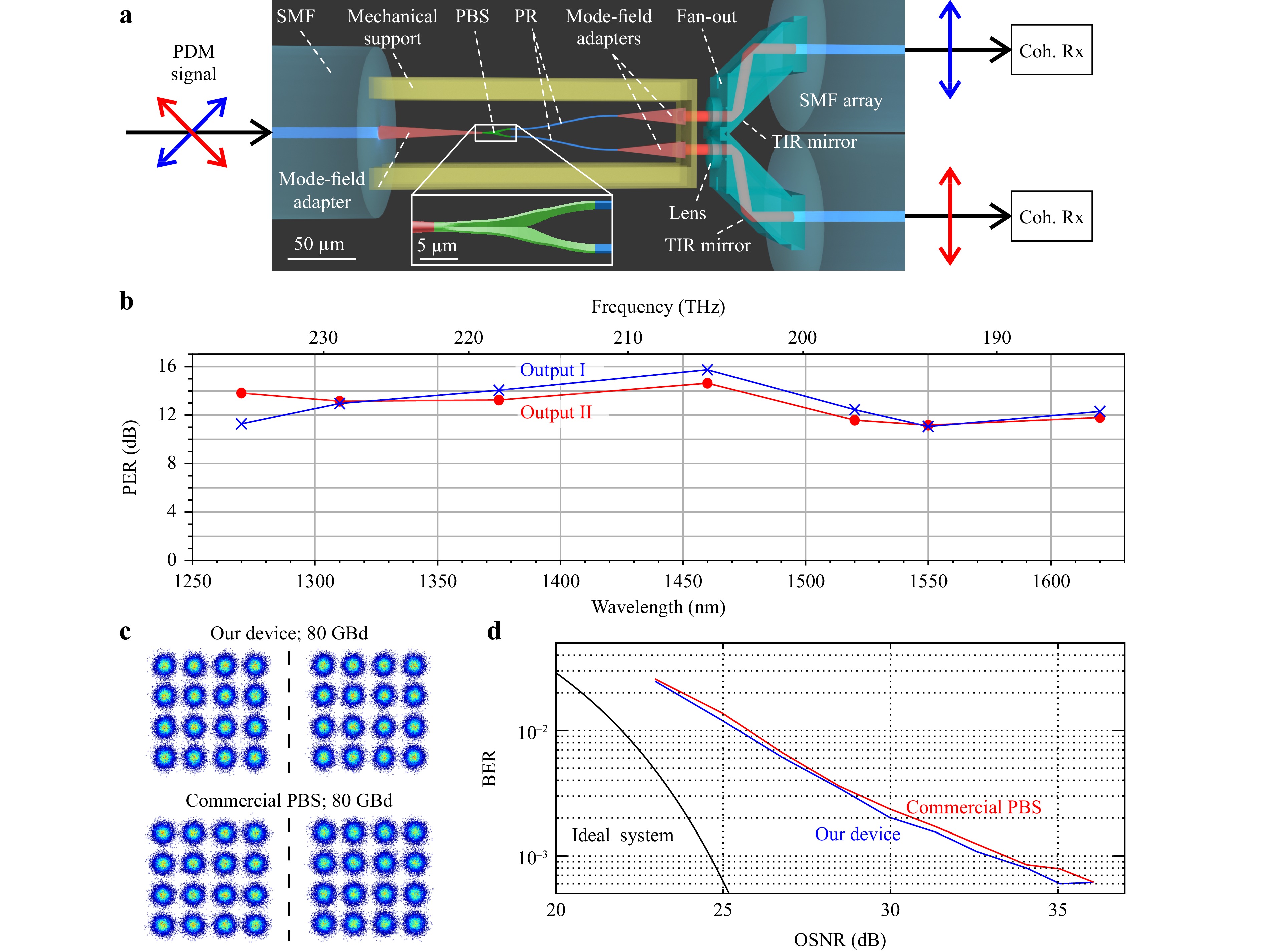
Fig. 4 Experimental setup and results of proof-of-concept data transmission experiment. a Simplified experimental setup: The polarisation-division-multiplexed (PDM) 16QAM signal is fed to an SMF having a mode-field adapter and a 3D-printed polarisation beam splitter (PBS) on its facet. The PBS is additionally equipped with 3D-printed polarisation rotators (PR) in the form of twisted waveguides, which rotate the polarisations in both output ports to an identical direction. We simultaneously probe the two output signals by a fan-out structure that is 3D-printed on a second SMF array. The fan-out consists of two lenses and two pairs of total-internal-reflection (TIR) mirrors to adapt the 25 µm pitch of the PBS/PR outputs to the 127 µm pitch of the SMF in the array. The signals are subsequently decoded by a pair of commercial coherent receivers (Coh. Rx). To benchmark our device, we repeat the experiment by replacing the PBS/PR assembly and the fan-out by a commercial fibre-coupled PBS. b Measurement of the PER for both outputs: The PER is better than 11 dB in the wavelength range 1270−1620 nm, which was only limited by the tuning range of the underlying laser sources. c Constellation diagrams of received 80 GBd 16QAM signals for an optical signal-to-noise ratio (OSNR) of 36 dB. Upper row: experiment with our device. Lower row: experiment with the commercial PBS. d Bit-error-ratio (BER) vs. OSNR. Black: Theoretical curve for an ideal transmission system. Blue: Experiment with our 3D-printed PBS/PR assembly. Red: Experiment with the commercial PBS. Our device does not introduce an OSNR penalty with respect to the commercial PBS. At a BER of 1.25 × 10⁻², which corresponds to the threshold of forward error correction with 15 % coding overhead, our transmission setup exhibits an implementation penalty of approximately 3 dB, see Supplementary Information Section S5 for details.
To demonstrate the technical viability of the 3D-printed PBS, we performed a polarisation-division multiplexing (PDM) data transmission experiment that emulates the application scenario illustrated in Fig. 1. The experimental setup and results are shown in Figs. 4a, c, d. Details of the experimental setup can be found in Supplementary Information, Section S5. The experiment relied on a PBS/PR combination, as used in the previous experiment, complemented by an additional fan-out structure, see Fig. 4a. This fan-out structure is 3D-printed on a second fibre array and allows to simultaneously couple both PBS outputs to a pair of outgoing SMF with a standard pitch of 127 µm. The fan-out structure is equipped with two lenses with a pitch of 25 µm that pick-up light from the two PBS outputs, followed by a pair of total-internal-reflection (TIR) mirrors in each path to adjust the lateral offset of the beams at the output. At $ \lambda =1550\;\mathrm{n}\mathrm{m} $, the measured insertion losses of the two channels of the fan-out are 1.2 dB and 1.9 dB, with a crosstalk between channels below –46 dB.
In the data transmission experiment, we launched a 16QAM PDM signal at a symbol rate of 80 GBd and a centre wavelength of λ = 1550 nm into the PBS/PR input, and fed the two output signals of the device to a pair of coherent receivers (see Supplementary Information Section S5 for details). We performed the experiment both with our 3D-printed PBS assembly and with a commercially available fibre-coupled PBS having a PER in excess of 30 dB. In both cases, we swept the optical signal-to-noise ratio (OSNR) at the input of the PBS and recorded constellation diagrams along with the corresponding bit error ratios (BER), as shown in Figs. 4c, d. At a BER of 1.25 × 10⁻², our transmission setup exhibits an OSNR penalty of approximately 3 dB with respect to an ideal intradyne transmission system, as shown in Fig. 4d. This rather high implementation penalty occurs because our experiment had to rely on a heterodyne receiver scheme, which leads to additional impairments caused by amplified spontaneous emission (ASE) noise that would not be observed in a more commonly used intradyne receiver. The additional ASE impairments are responsible for approximately 2 dB of the measured 3 dB OSNR implementation penalty (see Supplementary Information Section S5 for details). Nevertheless, our experiments show that the 3D-printed PBS/PR assembly does not introduce any additional OSNR penalty with respect to commercial PBS, although the respective PER differ significantly. This may be attributed to the fact that the polarisation-sensitive mixing of data signals with the LO of the coherent optical receiver in combination with the digital polarisation demultiplexing algorithms of the PDM receiver can easily compensate for the finite PER of our 3D-printed PBS. Hence, even though there is still room for improvement in the performance of our 3D-printed PBS/PR assemblies, the current devices already offer an attractive route towards highly scalable ultra-compact dual-polarisation receivers, as shown in Fig. 1.
Finally, we compared the performance of our PBS/PR assembly with that of competing approaches. Our device exhibited a measured PER of better than 11 dB for wavelengths between 1270 and 1620 nm. The insertion loss is between 3.8 dB and 4.4 dB at a wavelength of 1550 nm and may be further reduced towards 2.5 dB, see Section S2 of the Supplementary Information. These loss figures are comparable to those obtained from polarisation-splitting grating couplers (PS-GC) with backside metal mirrors12, which exhibit measured insertion losses of 2.4 dB for both polarisations at a wavelength of 1550 nm. However, note that these insertion losses were measured by optimising the position of the optical fibre with respect to the PS-GC individually for each polarisation, and that they are expected to increase to 3.8 dB for a fixed fibre position12. Note also that the PS-GC is intrinsically narrowband and the insertion loss increases by at least 7 dB within a wavelength range of 60 nm, as shown in Fig. 3 of Ref. 12. Moreover, PS-GC often leads to technically unfavourable packaging geometries, with fibres mounted too close to the surface-normal position of the chip. Nevertheless, the measured PER of the PS-GC is 25 dB at a wavelength of 1550 nm, which clearly outperforms our current devices; however, we believe that these deficiencies can be overcome by further optimisation of the 3D-printed structures (see Section S2 for details). Other approaches9,34,35 rely on waveguide-based polarisation splitters and rotators that can be fabricated in multilayer silicon nitride structures. Such devices were demonstrated34,35 to exhibit a PER greater than 16 dB within a 60 nm-wide wavelength range35, whereas the measured insertion losses34 were approximately 1 dB. Similar performance was obtained7 for PBS/PR structures based on mode conversion in standard silicon photonic (SiP) waveguides, offering a 13 dB PER and a 1.5 dB insertion loss over a wavelength range of 50 nm. These losses, however, do not include the coupling between an optical fibre and an on-chip waveguide, which would typically add another 1.5–2 dB of loss36, thus leading to overall losses of 3–3.5 dB. These values are comparable to the losses achieved using our devices. Note also that integrated waveguide-based PBS/PR rely on rather long structures with typical lengths9,34,35 of 400 µm to 800 µm. Hence, our approach should also be able to compete with PBS/PR concepts based on rather large on-chip structures in terms of both PER and insertion loss.
-
We demonstrated 3D-printed waveguide-based PBSs that can be efficiently integrated into the chip-chip and fibre–chip interfaces of optical assemblies. The devices rely on adiabatic Y-branches of geometrically birefringent waveguides with high-aspect-ratio cross sections and can be complemented by PRs that exploit twisted 3D freeform waveguides. PBS/PR can be efficiently fabricated by direct-write two-photon lithography together with other 3D-printed elements such as photonic wire bonds19,20, 3D-printed microlenses16–18,23,24, or 3D-printed waveguide overpasses37. In our proof-of-concept experiments, we demonstrated broadband operation in the wavelength range of 1270–1620 nm, which is limited only by the available equipment. We further proved the practical viability of the concept in a high-speed data transmission experiment in which our 3D-printed PBS/PR assemblies were used to separate polarisation-multiplexed data signals at the receiver. The quality of the received signals was on par with that obtained using a conventional high-performance fibre-coupled PBS. Although this concept leaves room for further optimisation, we believe that the 3D-printed PBS/PR can pave the way for efficient polarisation manipulation in integrated optical systems with unprecedented compactness and scalability.
-
For the simulations shown in Fig. 2, the 3D structure of the PBS was modelled using a commercially available 3D numerical time-domain solver (CST Studio Suite, Dassault Systèmes, Vélizy-Villacoublay, France). The final design of the PBS was the result of manual optimisation based on several parameter sweeps.
-
All 3D-printed structures were fabricated using a home-built two-photon lithography system equipped with a 63× microscope objective lens (numerical aperture 1.4, field number 25 mm) and galvanometer mirrors for rapid beam movement in the lateral directions. As the lithography light source, we used a femtosecond laser with a pulse length of less than 80 fs (C-Fiber 780 Femtosecond Fiber Laser; Menlo Systems GmbH, Planegg, Germany) and a repetition rate of 100 MHz. The lithography system is equipped with dedicated control software that allows for precise localisation of the optical fibre core, as well as for automated fabrication of the PBS with high shape fidelity. The system further comprises a confocal imaging unit using the lithography laser and its beam deflectors for the acquisition of 3D images that are perfectly aligned to the lithography coordinate system and hence to any lithographically fabricated structure. For confocal imaging, the laser power was reduced to avoid unwanted polymerisation in the photoresist. In the lithography process, a liquid negative-tone photoresist (Nanoscribe IP-Dip, refractive index of the unexposed material n = 1.52 at 780 nm; see Ref. 38) simultaneously acted as an immersion medium for the objective lens. The unexposed photoresist was removed by a two-step development process using propylene-glycol-methyl-ether-acetate (PGMEA) as the developer for 20 min, followed by rinsing in isopropyl alcohol (2-propanol).
Because of the confocal imaging unit, the alignment accuracy of the volumetric pixels (voxels) of the two-photon lithography system with respect to the facets of the connected optical devices is typically better than 100 nm. The size of the smallest printable structural feature is specified by the resolution of the system, which is dictated by the voxel shape and size. In our lithography system, the voxel is an ellipsoid with two principal axes of 400 nm in the lateral direction and the third principal axis of about 1 µm in the axial direction of the printing beam. In the future, the resolution of two-photon lithography systems may be further improved by using super-resolution 3D-lithography techniques inspired by the concept of stimulated-emission-depletion (STED) microscopy39. The current fabrication time for 3D-printed PBS strongly depends on the shape and volume of the printed structure. For the structures shown in Fig. 4a, printing took approximately 10 min, including the rather large mechanical support structures, which required approximately 80% of the printing time, as well as the massive mode-field adapters. The printing time of the PBS waveguide sections was approximately one minute, and we expect that dedicated acceleration techniques can considerably reduce this time, thereby paving the way for high-throughput production of 3D-printed PBS in advanced photonic assemblies.
The fabricated structures were found to be reasonably robust for practical applications. Specifically, during the experiments, our laboratories were subjected to significant temperature fluctuations that did not affect the performance of the structure. The long-term stability of 3D-printed micro-optical structures has been previously demonstrated for both photonic wire bonds (PWB)20 and facet-attached microlenses23. Such 3D printed structures are remarkably robust with respect to vibrations, and we tested this aspect in the context of facet-attached micro-lenses (FaMLs)23 for random vibrations and accelerations of up to 500 g (see Ref. 23). However, direct mechanical contact with the structure will irreversibly destroy it and should be avoided.
-
For PRs and output waveguides, careful planning of the 3D trajectory is important to ensure efficient coupling between the PBS and other optical structures. To this end, we used a parameterised trajectory and optimised it for low curvature, and hence, low radiation loss. Along this trajectory, the waveguide cross section is extruded to form a 3D model of the structure, which is then lithographically fabricated. Low-loss coupling between PBS and the standard SMF (Corning SMF-28) at its input is achieved by a linearly tapered mode-field adapter, designed for a mode-field diameter (MFD) of (10.3 ± 0.4) µm at 1550 nm at the fibre side. The MFD is defined as the diameter at which the intensity decreases to 1/e² of its maximum value measured at the centre of the fibre core. These methods were derived from the photonic wire bonding process, the details of which can be found in Ref. 20.
-
To characterise the 3D-printed PBS in Fig. 3, we used an IR camera (Goldeye G-032 SWIR, Allied Vision) attached to a microscope (DMRXA with a variable zoom unit DMRD, Leica/Leitz) equipped with an IR objective (LMPlan IR 100×/0.80NA, Olympus). An optional rotatable linear polariser (LPIREA100-C, Thorlabs, PER > 34 dB at 1550 nm) can be inserted into the collimated optical beam path of the microscope. Light generated by a tunable external-cavity laser (IQS-2600B, EXFO) was injected into the SMF, and the polarisation was adjusted using a standard fibre-based polarisation controller. Each acquired image was corrected for background signal observed when the laser was turned off.
-
The PER was measured using an optical component analyser (Keysight N7788B) comprising an integrated fast polarisation controller and a polarimeter. The polarisation controller randomly scrambles the polarisation state, thereby uniformly covering the entire Poincaré sphere. The polarisation state and power at the output of the PBS structure were measured simultaneously using the polarimeter (see Supplementary Information Section S2 for details). The PER was extracted from these measurements (see Supplementary Information, Section S4, for details). The PER was measured at seven discrete wavelengths between 1270 and 1620 nm using three tunable laser sources (Ando AQ4321D, TUNICS T1005-HP, Agilent 81600B).
-
In our data transmission experiments, we used four output channels from an AWG (Keysight M8194A) to generate the drive signals for the dual-polarisation IQ modulator (see Supplementary Information Section S5 for a sketch of the underlying experimental setup). The signals are derived from random bit patterns with different seeds, such that each polarisation carries uncorrelated data, and are pre-distorted to compensate for the measured frequency response of the transmitter. For the OSNR sweep, band-limited ASE noise was generated using an ASE source (Orion Laser Technology ASE-C/CL) and added to the data signal. The noise-loaded signal was then fed to the receiver, which comprised an erbium-doped fibre amplifier (EDFA) for preamplification, followed by a bandpass filter (full width at half maximum of 1 nm) to suppress out-of-band ASE noise. The signal was then fed into the 3D-printed PBS/PR, as shown in Fig. 4a, where the two orthogonal polarisation states were split and rotated. The two partial signals were then detected using a coherent heterodyne scheme, where the optical LO tone (Keysight N7714A) was tuned to the edge of the signal spectrum, and two balanced photodiodes (Finisar BPDV2150RQ) removed both the signal-signal and LO-LO interference (see Supplementary Information Section S5 for details). The photodiode outputs were digitised using a 256 GSa/s real-time oscilloscope (Keysight UXR1004A) and recorded for offline digital signal processing (DSP). In the first DSP step, the signals were shifted in frequency by the difference between the carrier and LO tones. After timing recovery, a 2 × 2 MIMO equaliser was used for polarisation demultiplexing, followed by carrier recovery (see Supplementary Information Section S5 for details). Finally, the signals are passed through a least-mean-square equaliser before decoding.
-
This work was supported by the Deutsche Forschungsgemeinschaft (DFG, German Research Foundation) in the framework of the Collaborative Research Center (CRC) Wave Phenomena (SFB 1173, project-ID 258734477) and under Germany´s Excellence Strategy via the Excellence Cluster 3D Matter Made to Order (EXC-2082/1 – 390761711), by the Bundesministerium für Bildung und Forschung (BMBF) within the projects PRIMA (# 13N14630), DiFeMiS (# 16ES0948), and Open6GHub (# 16KISK010), by the European Research Council (ERC Consolidator Grant ‘TeraSHAPE’, # 773248), by the Photonic Packaging Pilot Line PIXAPP (# 731954), by the Alfried Krupp von Bohlen und Halbach Foundation, by the Karlsruhe School of Optics and Photonics (KSOP), and by the Karlsruhe Nano-Micro Facility (KNMF). A.N. was supported by the Erasmus Mundus Joint Doctorate Programme Europhotonics (grant number 159224-1-2009-1-FR-ERA MUNDUS-EMJD).
Ultra-broadband polarisation beam splitters and rotators based on 3D-printed waveguides
-
Aleksandar Nesic1, *, ,
 ,
, - Matthias Blaicher1, 2,
- Pablo Marin-Palomo1,
- Christoph Füllner1,
- Sebastian Randel1,
- Wolfgang Freude1,
-
Christian Koos1, 2, 3, *, ,
- Light: Advanced Manufacturing 4, Article number: 22 (2023)
- Received: 19 December 2022
- Revised: 15 July 2023
- Accepted: 18 July 2023 Published online: 05 September 2023
doi: https://doi.org/10.37188/lam.2023.022
Abstract: Multi-photon lithography has emerged as a powerful tool for photonic integration, allowing to complement planar photonic circuits by 3D-printed freeform structures such as waveguides or micro-optical elements. These structures can be fabricated with a high precision on the facets of optical devices and enable highly efficient package-level chip–chip connections in photonic assemblies. However, plain light transport and efficient coupling is far from exploiting the full geometrical design freedom offered by 3D laser lithography. Here, we extended the functionality of 3D-printed optical structures to manipulation of optical polarisation states. We demonstrate compact ultra-broadband polarisation beam splitters (PBSs) that can be combined with polarisation rotators and mode-field adapters into a monolithic 3D-printed structure, fabricated directly on the facets of optical devices. In a proof-of-concept experiment, we demonstrate measured polarisation extinction ratios beyond 11 dB over a bandwidth of 350 nm at near-infrared telecommunication wavelengths around 1550 nm. We demonstrate the viability of the device by receiving a 640 Gbit/s dual-polarisation data signal using 16-state quadrature amplitude modulation (16QAM), without any measurable optical-signal-to-noise-ratio penalty compared to a commercial PBS.
Rights and permissions
Open Access This article is licensed under a Creative Commons Attribution 4.0 International License, which permits use, sharing, adaptation, distribution and reproduction in any medium or format, as long as you give appropriate credit to the original author(s) and the source, provide a link to the Creative Commons license, and indicate if changes were made. The images or other third party material in this article are included in the article′s Creative Commons license, unless indicated otherwise in a credit line to the material. If material is not included in the article′s Creative Commons license and your intended use is not permitted by statutory regulation or exceeds the permitted use, you will need to obtain permission directly from the copyright holder. To view a copy of this license, visit http://creativecommons.org/licenses/by/4.0/.

 DownLoad: