
2023 Vol. 4, No. 3
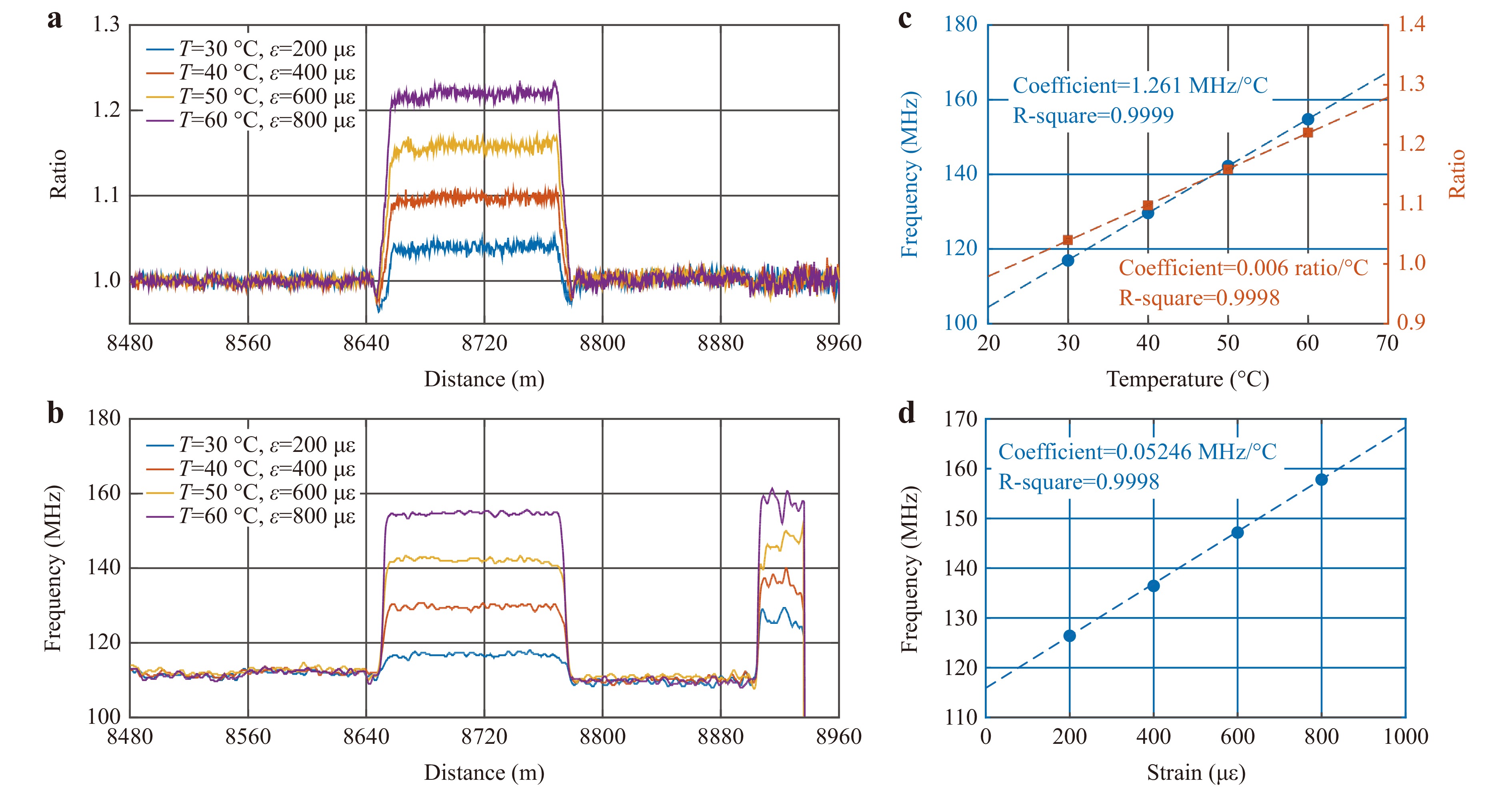
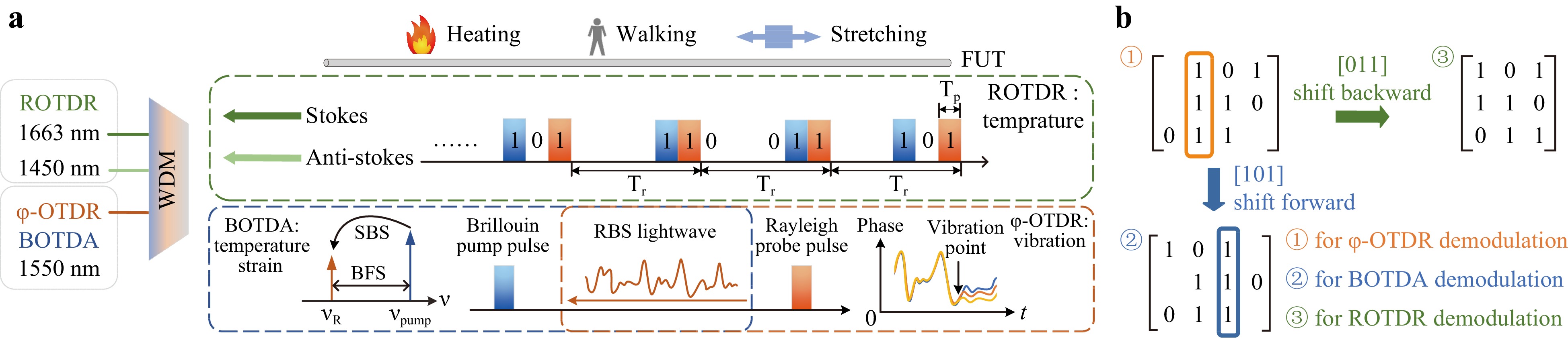
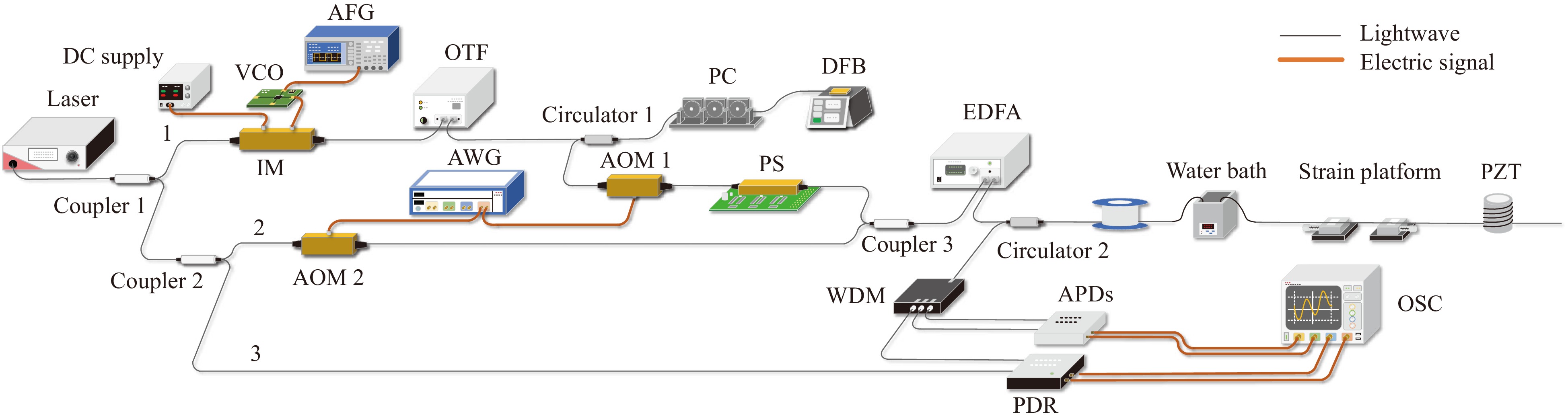
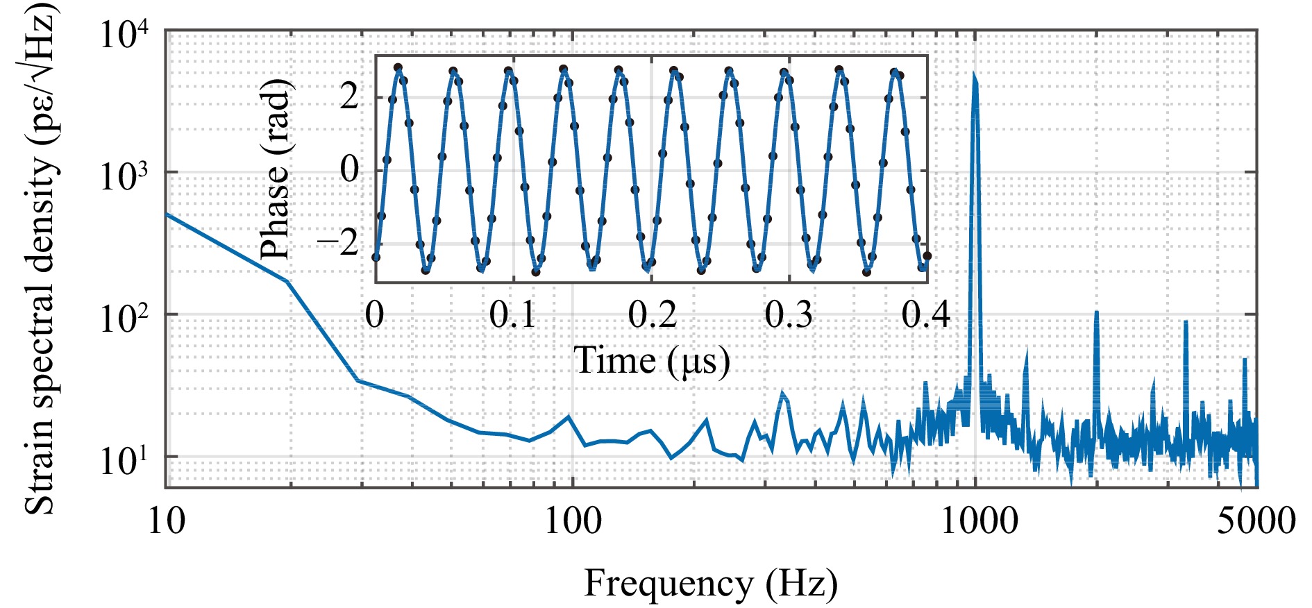
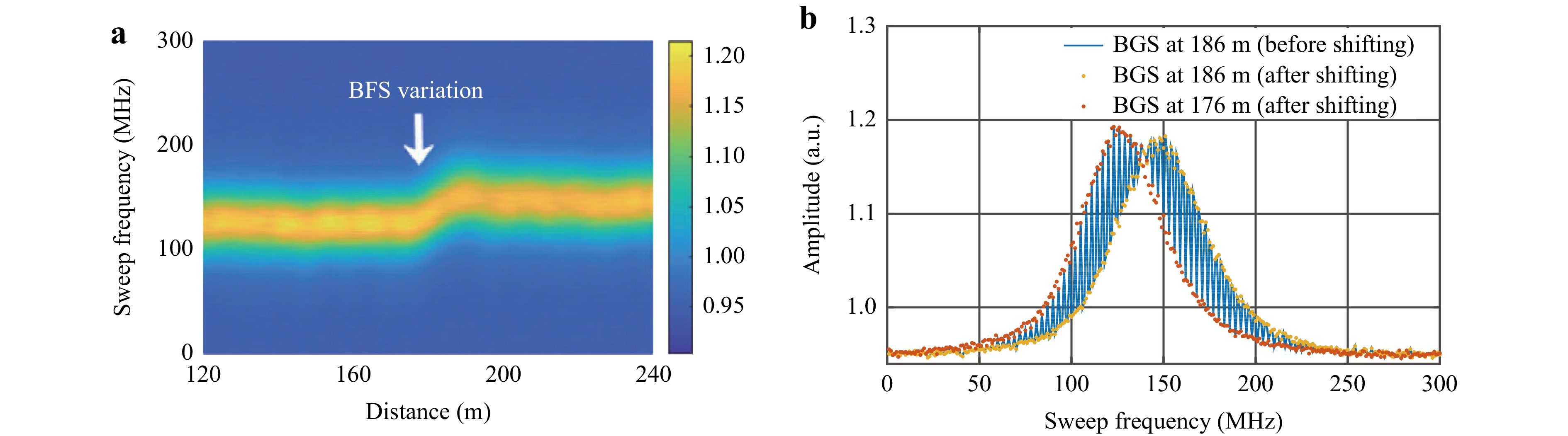
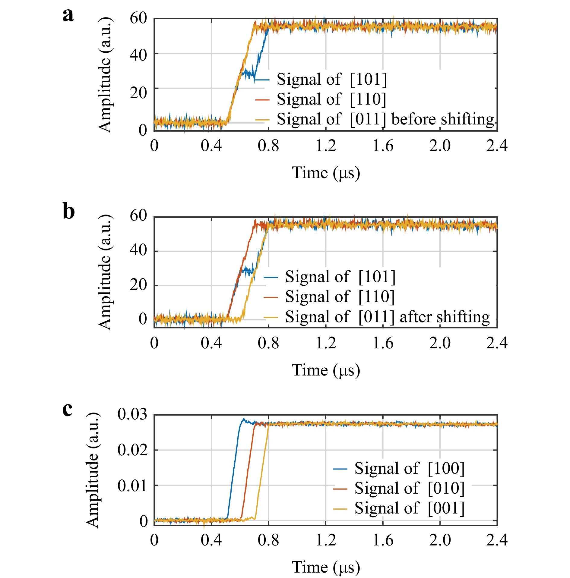
Backscattered lightwaves from an optical fibre are used to realise distributed fibre optic sensing (DFOS) systems for measuring various parameters. Rayleigh, Brillouin, and Raman backscattering provide different sensitivities to different measurands and have garnered the attention of researchers. A system combining the three principles above can effectively separate the measured strain and temperature completely as well as provide measurements of both dynamic and static parameters. However, the combined system is extremely complicated if the three systems are independent of each other. Hence, we propose a single-end hybrid DFOS system that uses two successive pulses to realise the Brillouin amplification of Rayleigh backscattering lightwaves for combining Rayleigh and Brillouin systems. A 3-bit pulse-coding method is employed to demodulate the Raman scattering of the two pulses to integrate Raman optical time-domain reflectometry into the hybrid system. Using this hybrid scheme, a simultaneous measurement of multiple parameters is realised, and a favourable measurement accuracy is achieved.
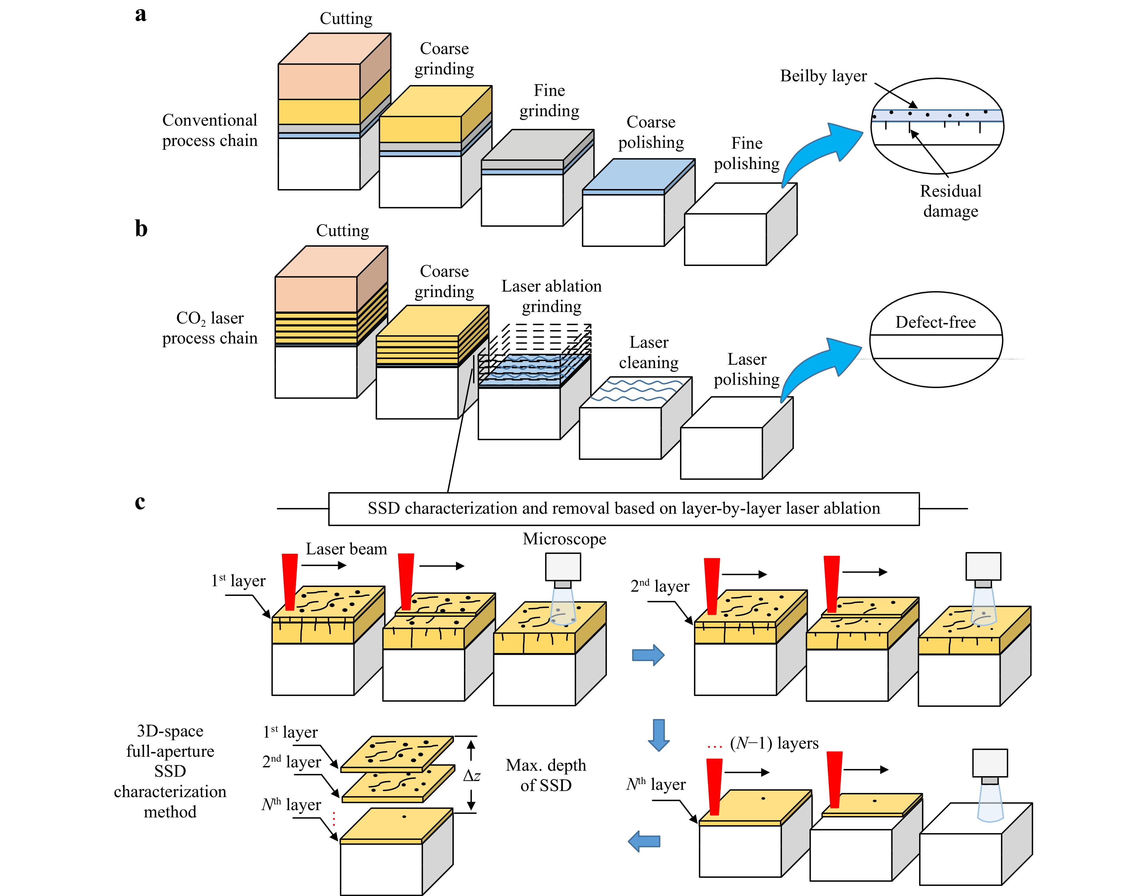
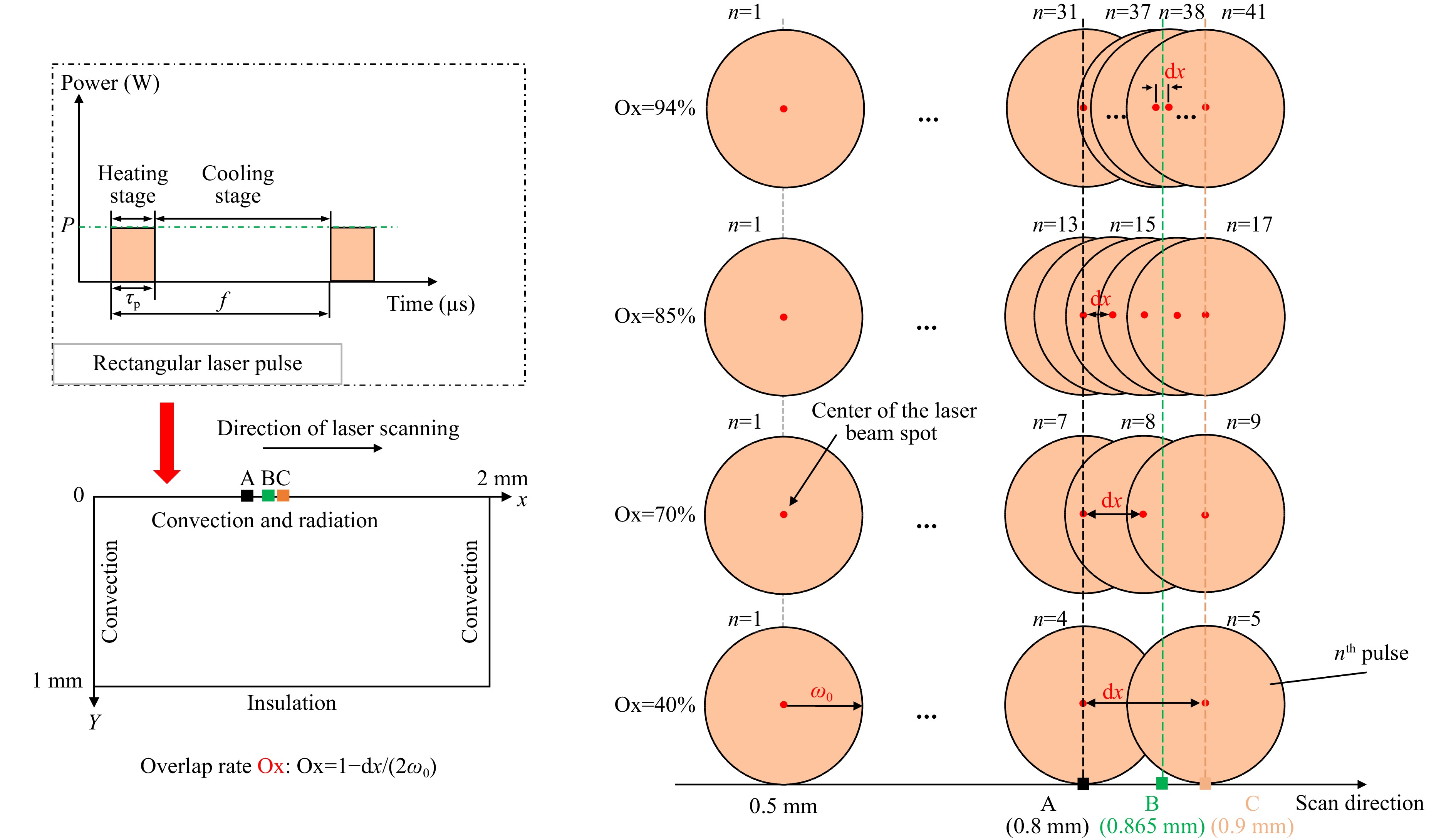
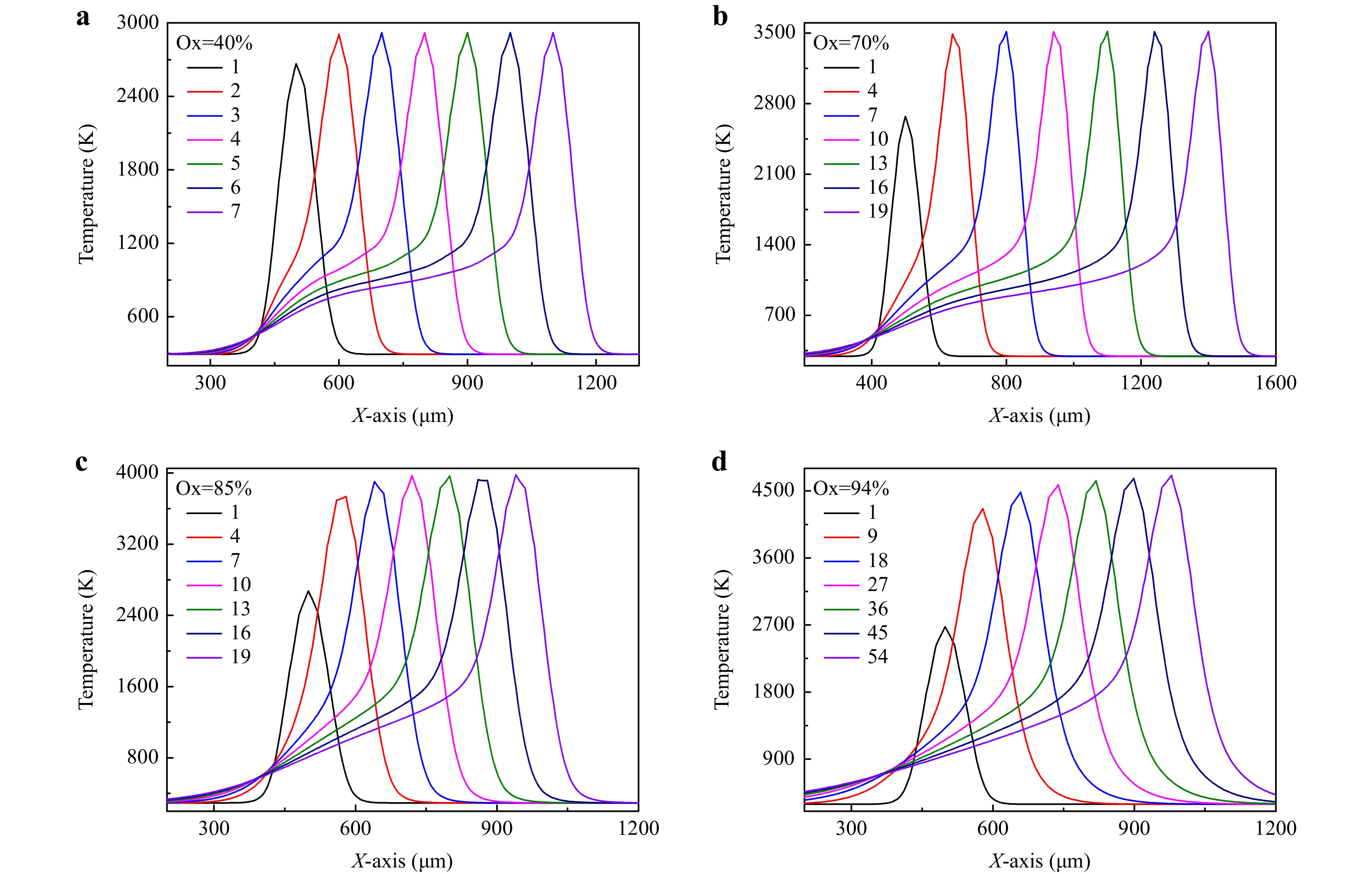
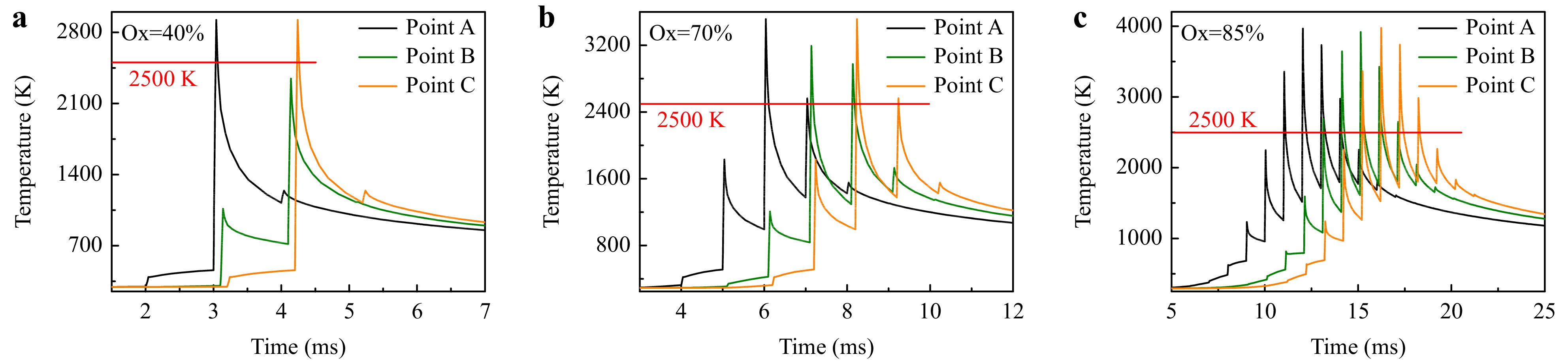
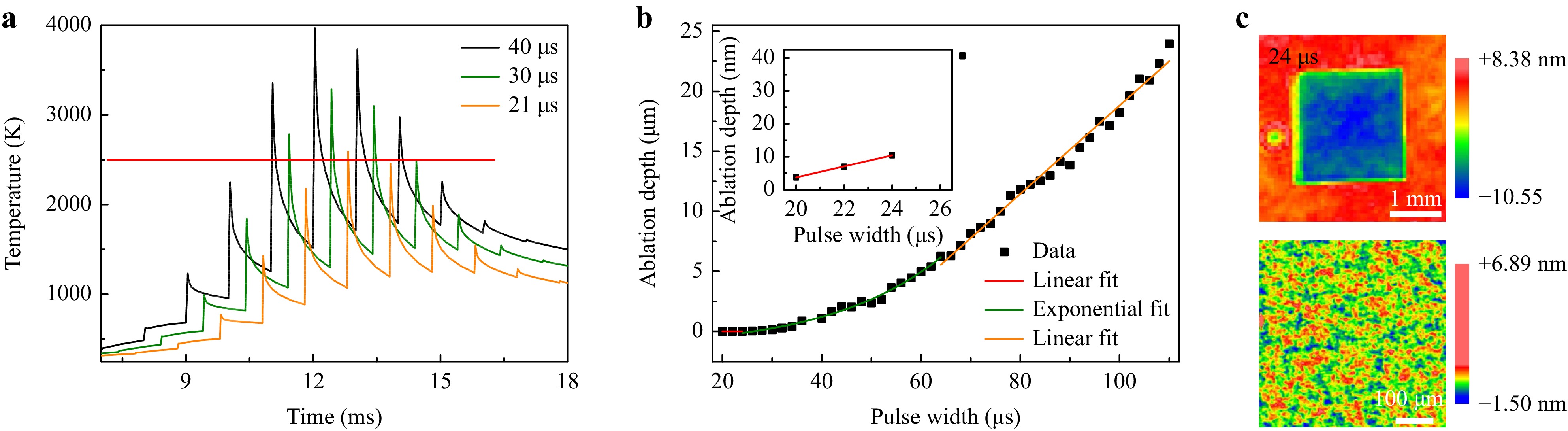
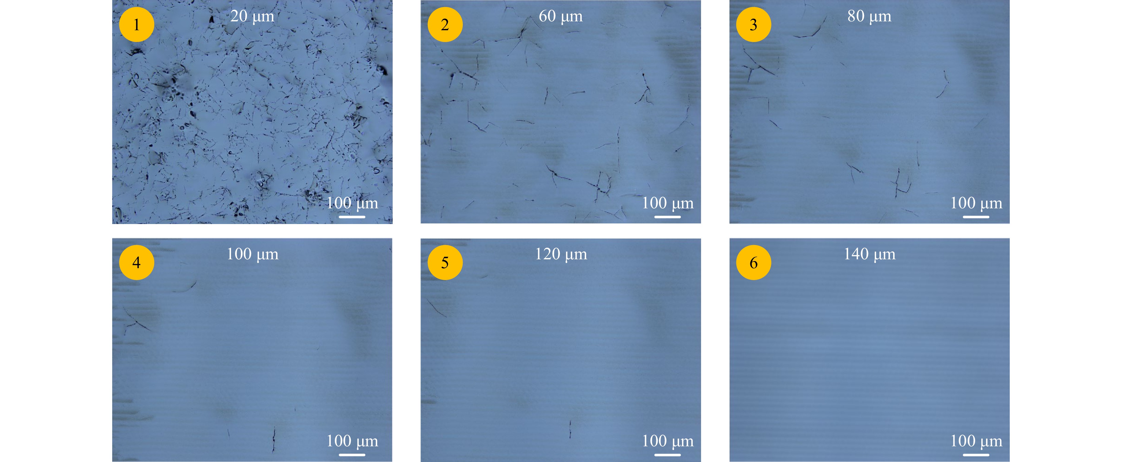
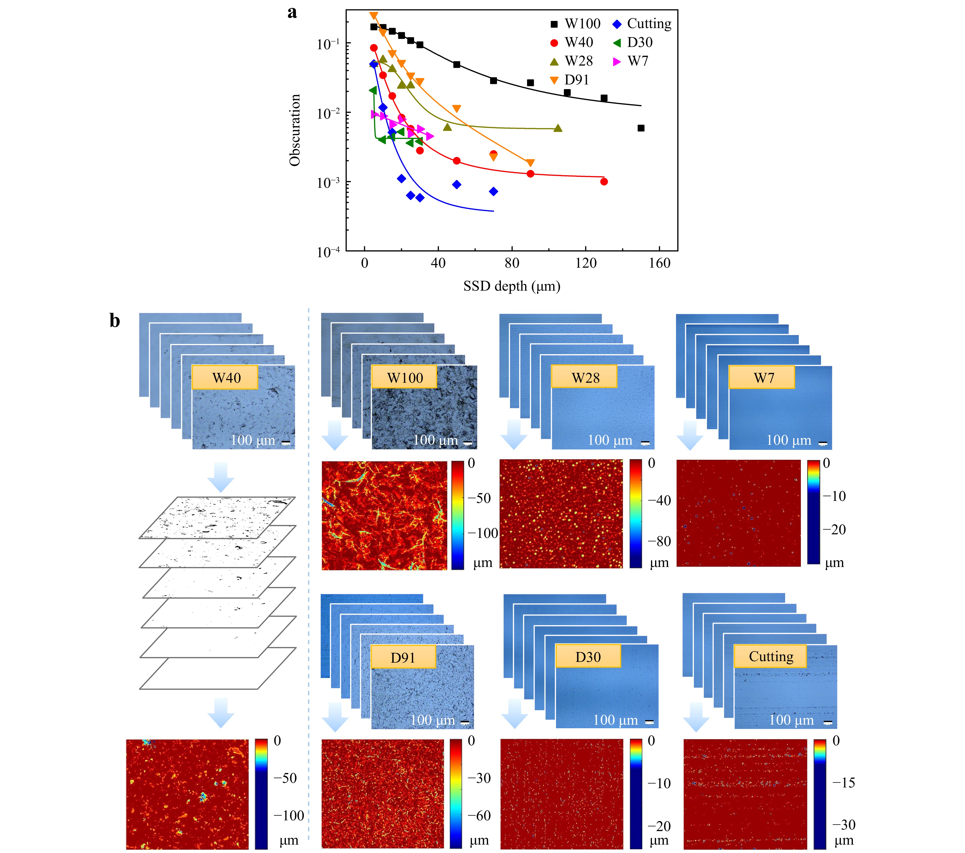
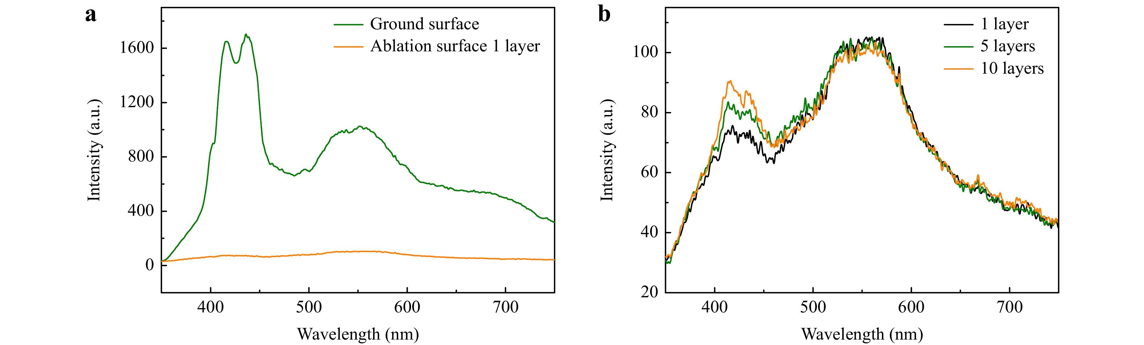
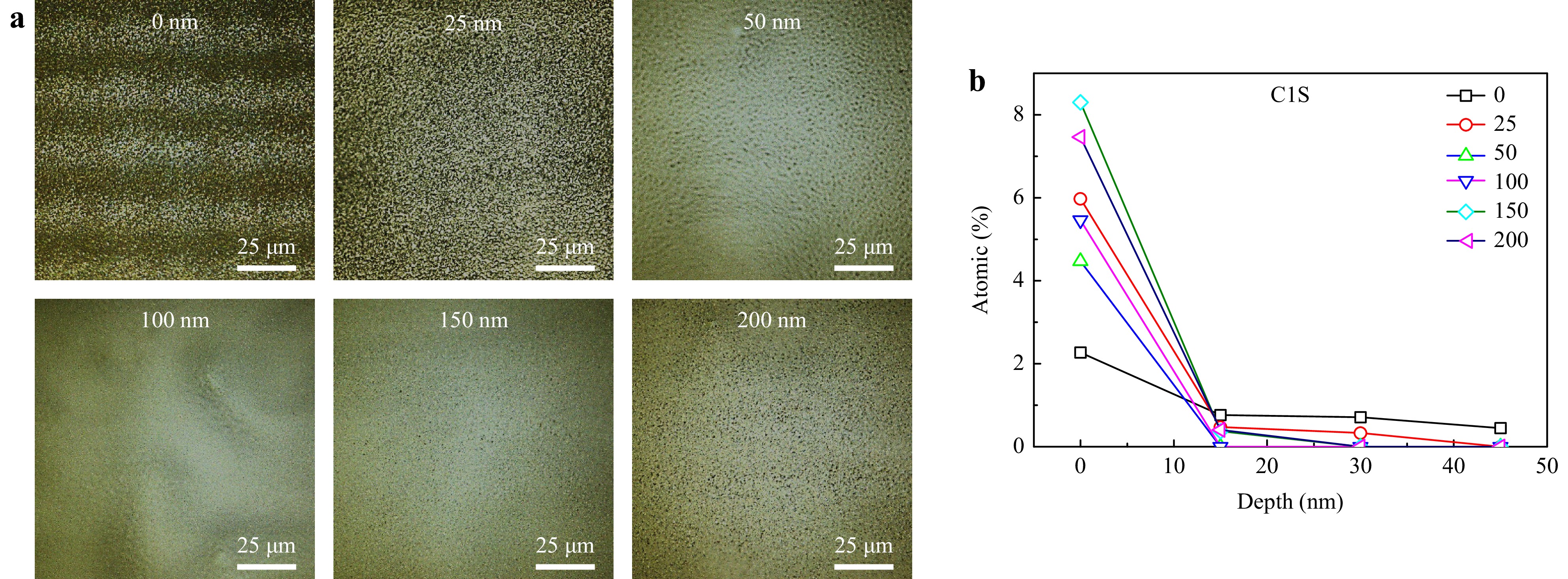
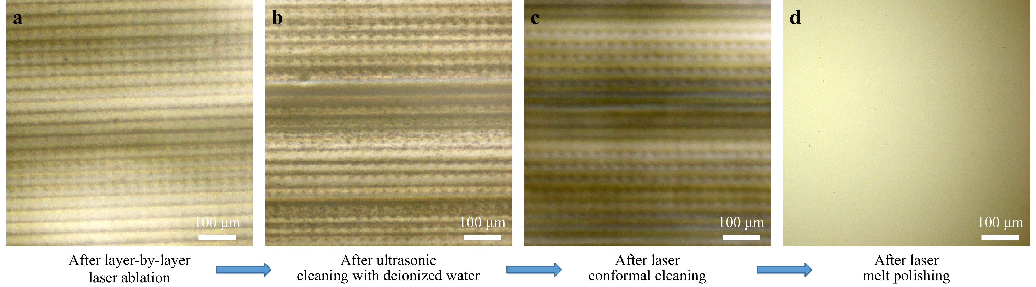
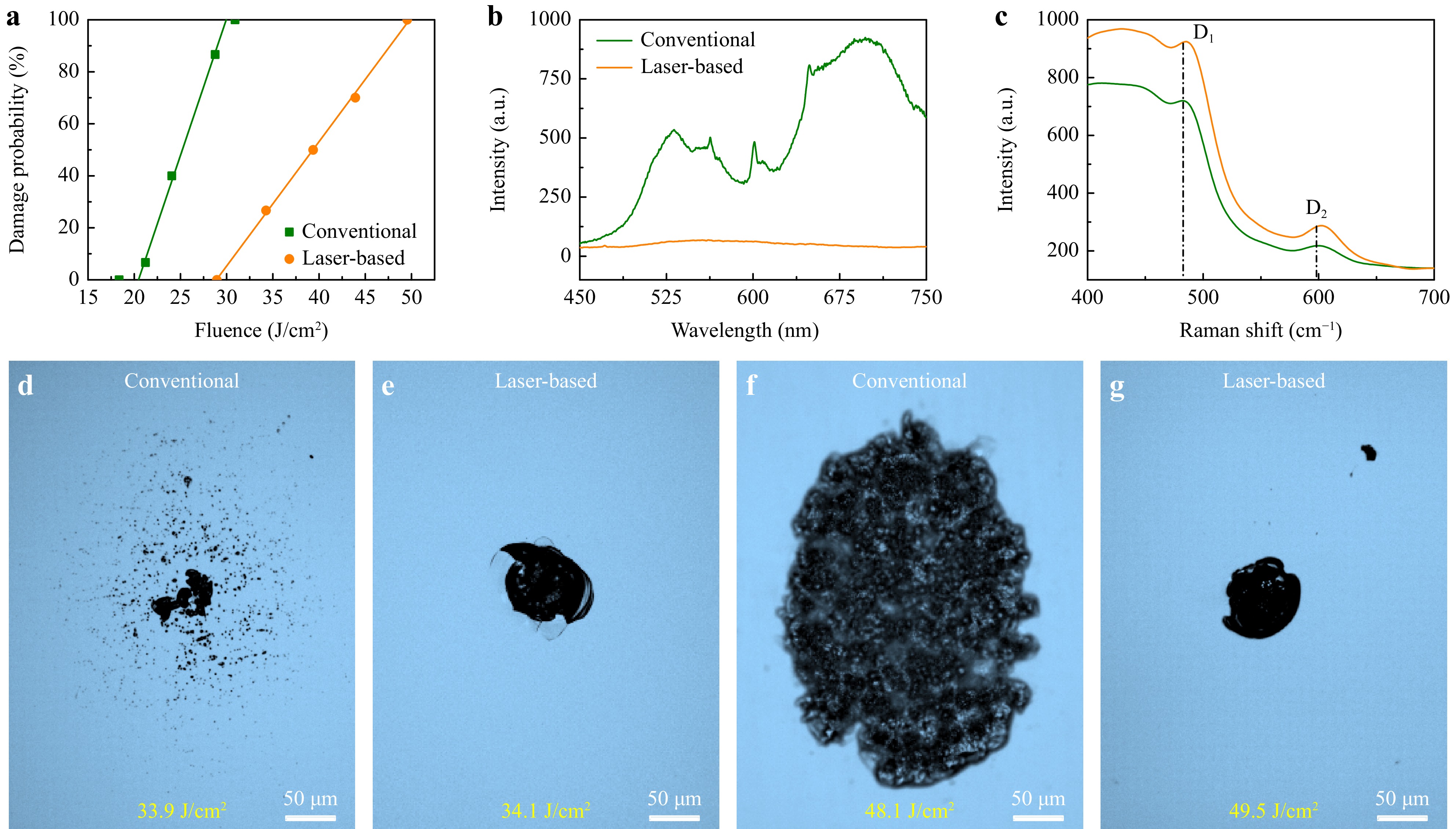
Residual processing defects during the contact processing processes greatly reduce the anti-ultraviolet (UV) laser damage performance of fused silica optics, which significantly limited development of high-energy laser systems. In this study, we demonstrate the manufacturing of fused silica optics with a high damage threshold using a CO2 laser process chain. Based on theoretical and experimental studies, the proposed uniform layer-by-layer laser ablation technique can be used to characterize the subsurface mechanical damage in three-dimensional full aperture. Longitudinal ablation resolutions ranging from nanometers to micrometers can be realized; the minimum longitudinal resolution is < 5 nm. This technique can also be used as a crack-free grinding tool to completely remove subsurface mechanical damage, and as a cleaning tool to effectively clean surface/subsurface contamination. Through effective control of defects in the entire chain, the laser-induced damage thresholds of samples fabricated by the CO2 laser process chain were 41% (0% probability) and 65.7% (100% probability) higher than those of samples fabricated using the conventional process chain. This laser-based defect characterization and removal process provides a new tool to guide optimization of the conventional finishing process and represents a new direction for fabrication of highly damage-resistant fused silica optics for high-energy laser applications.
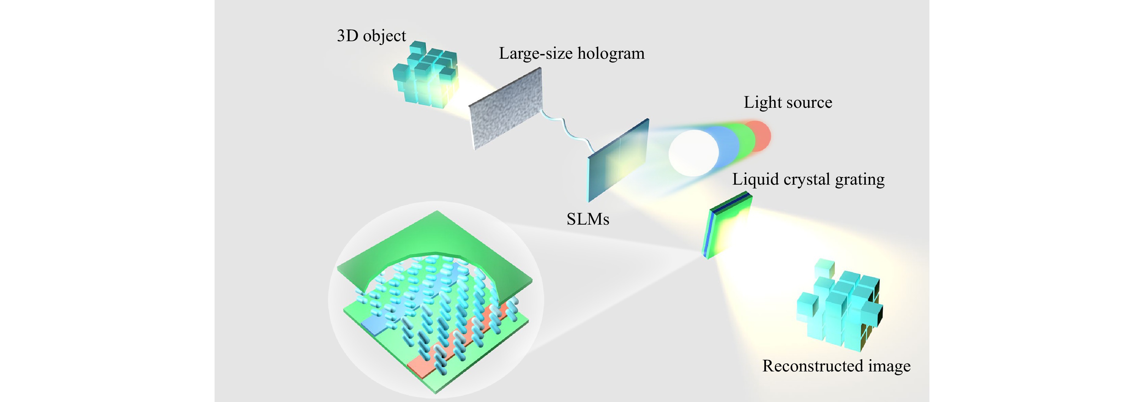
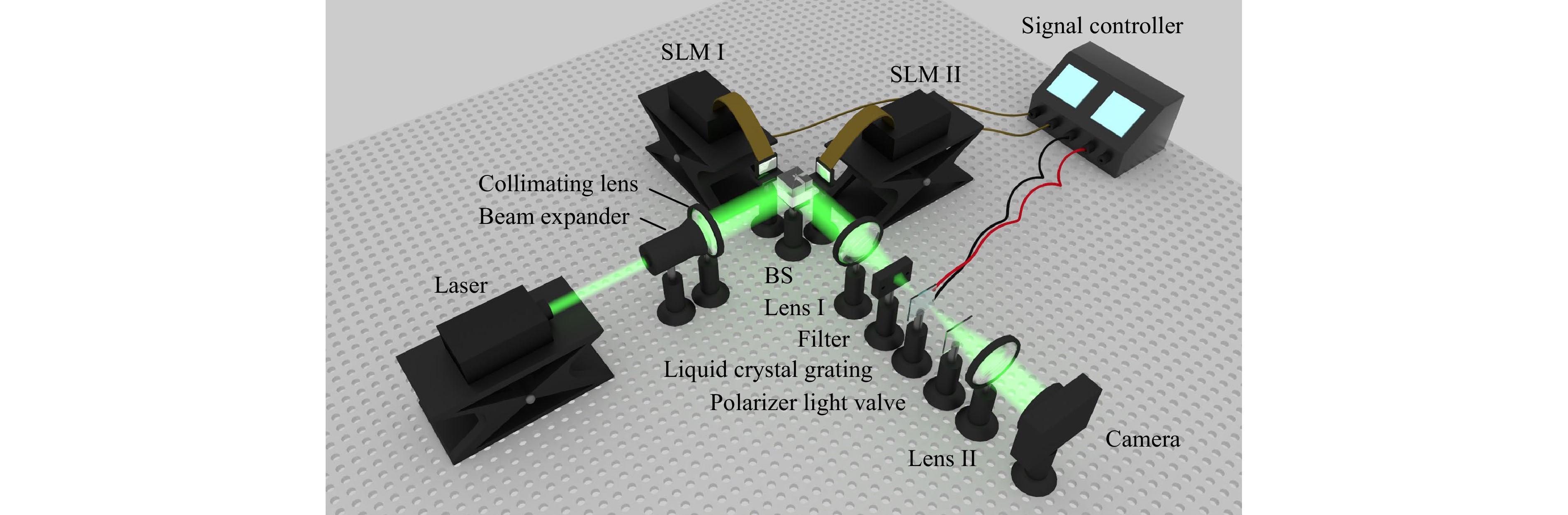
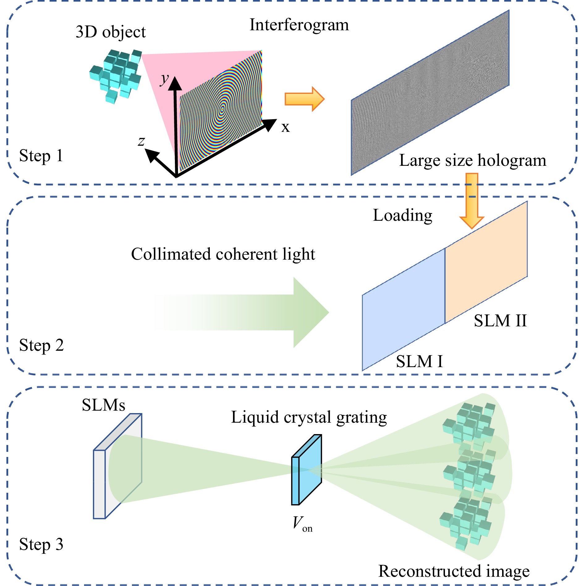
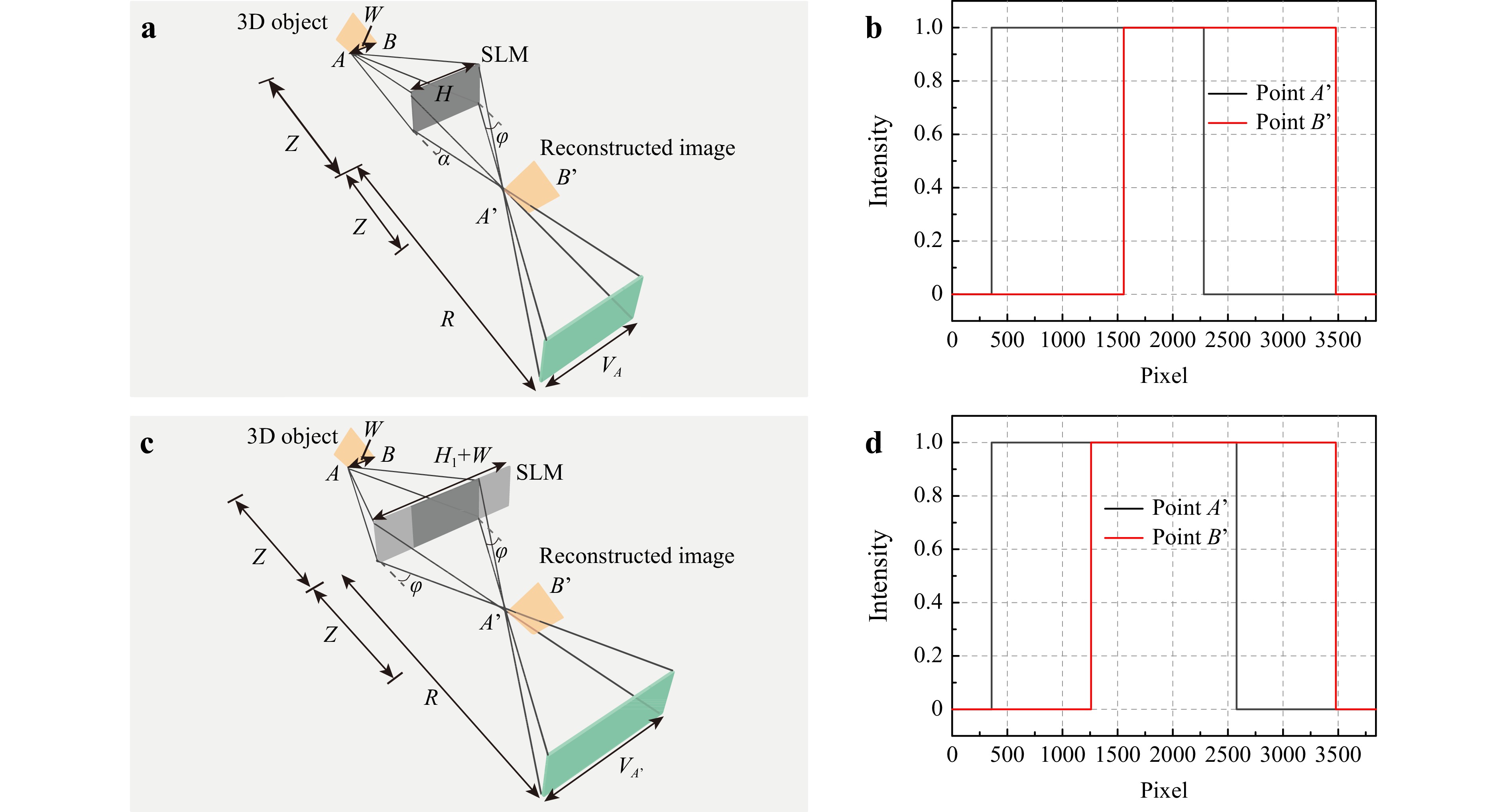
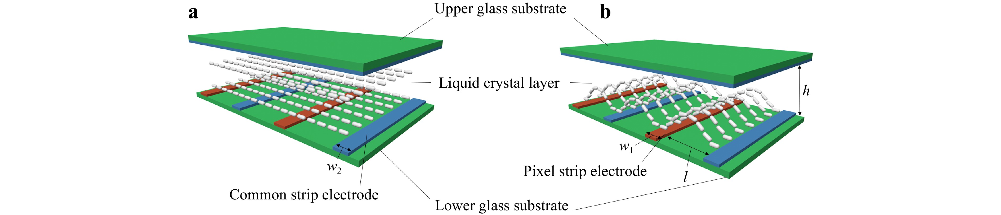
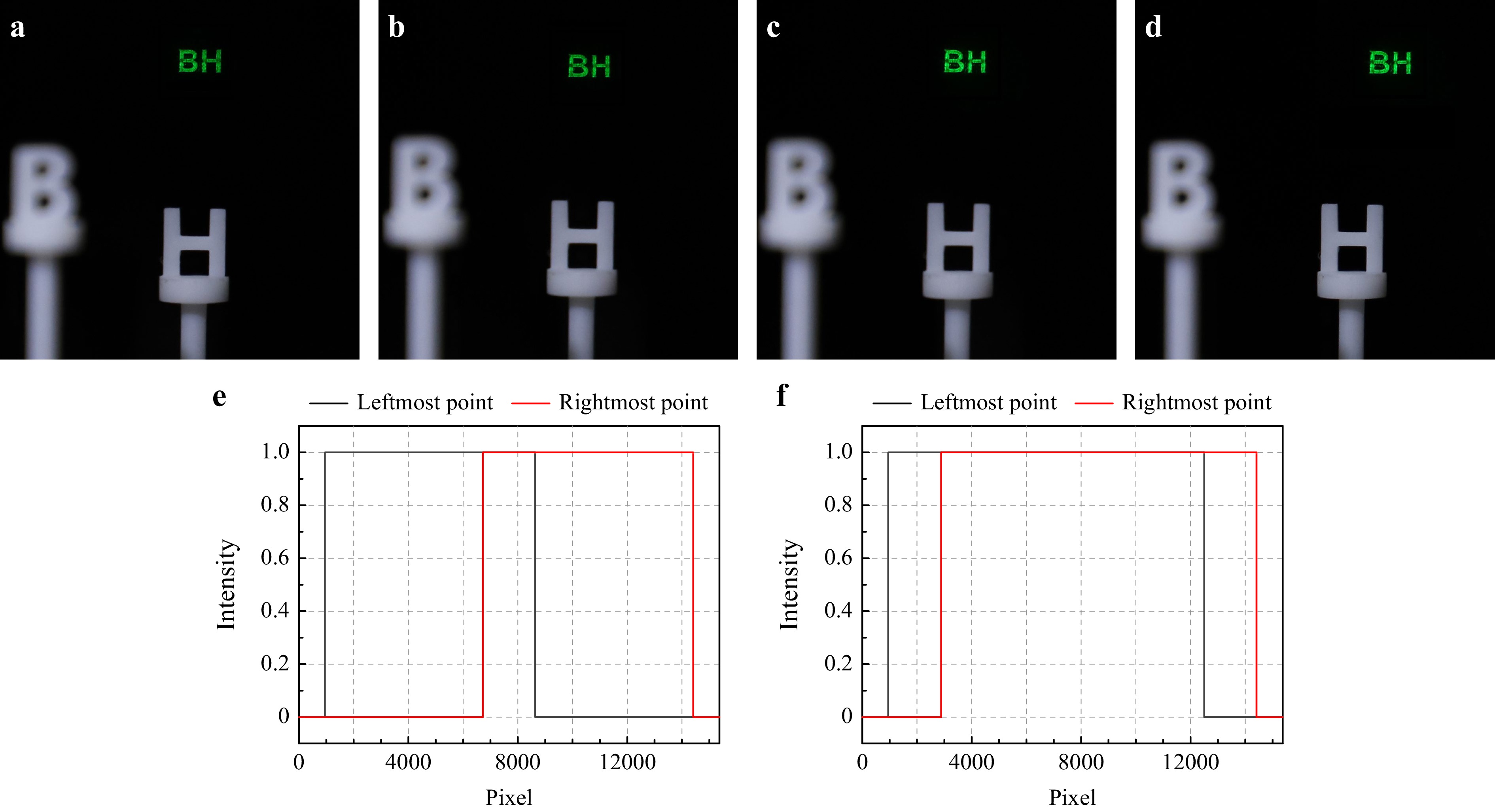
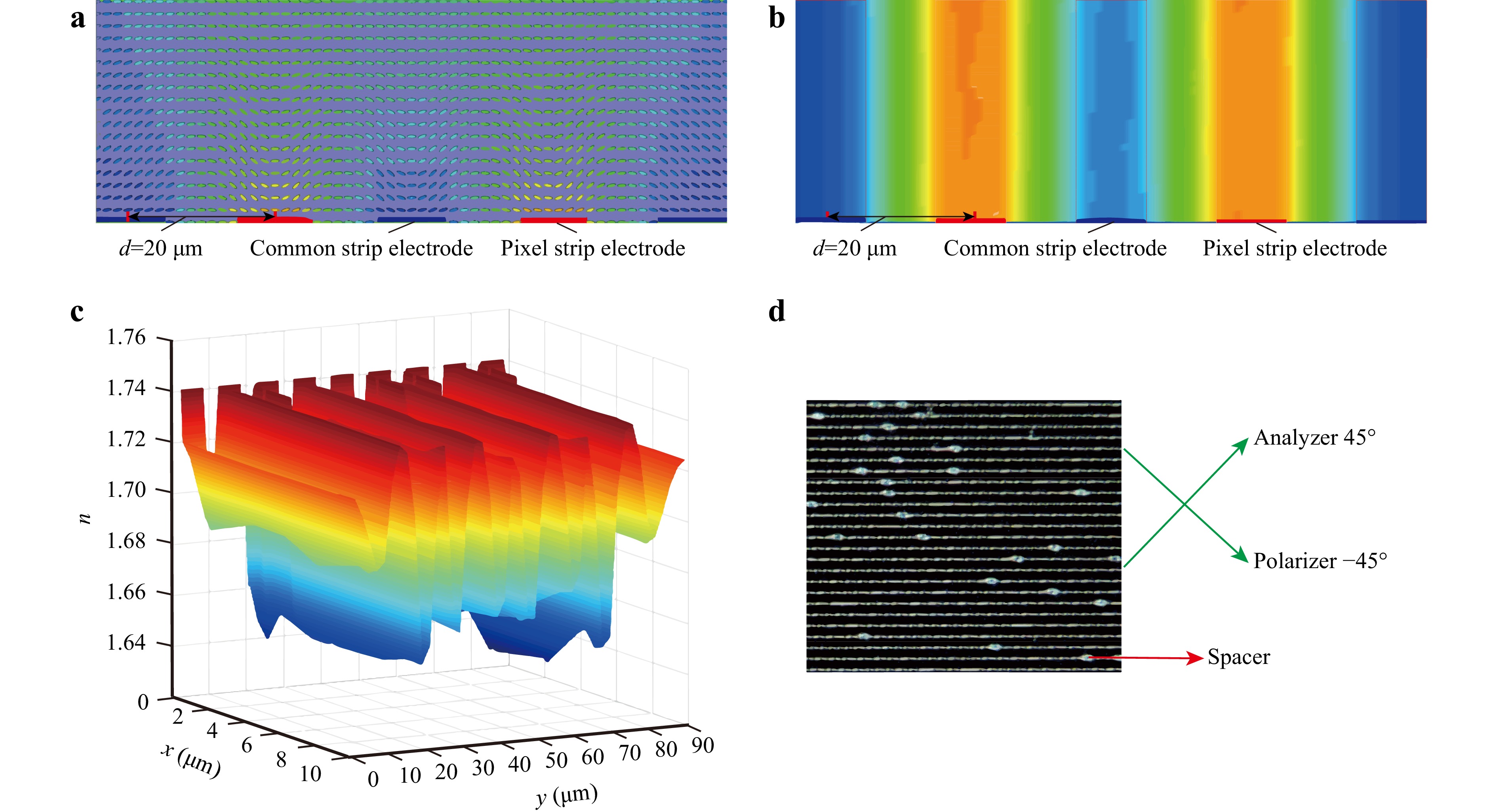
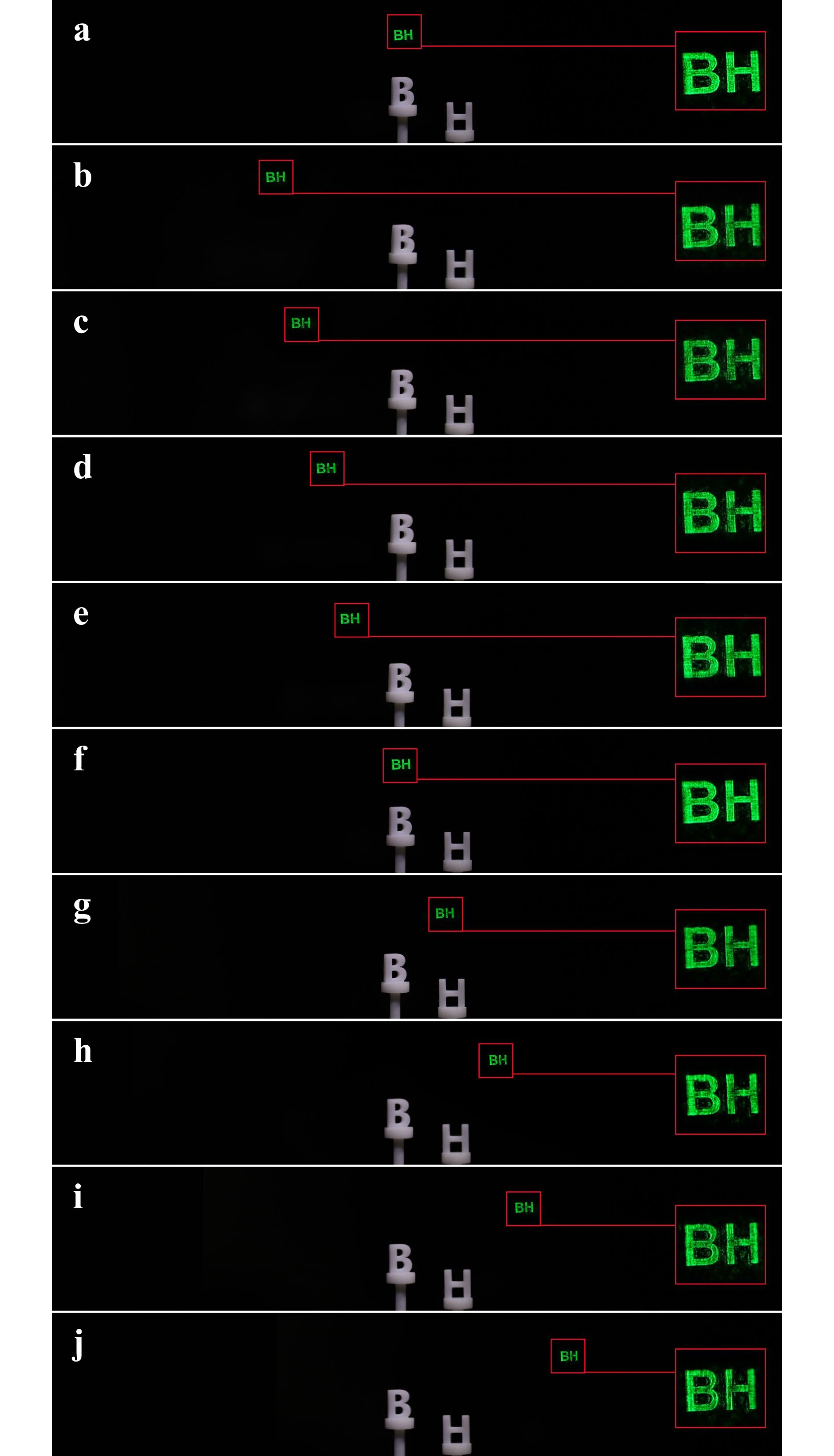
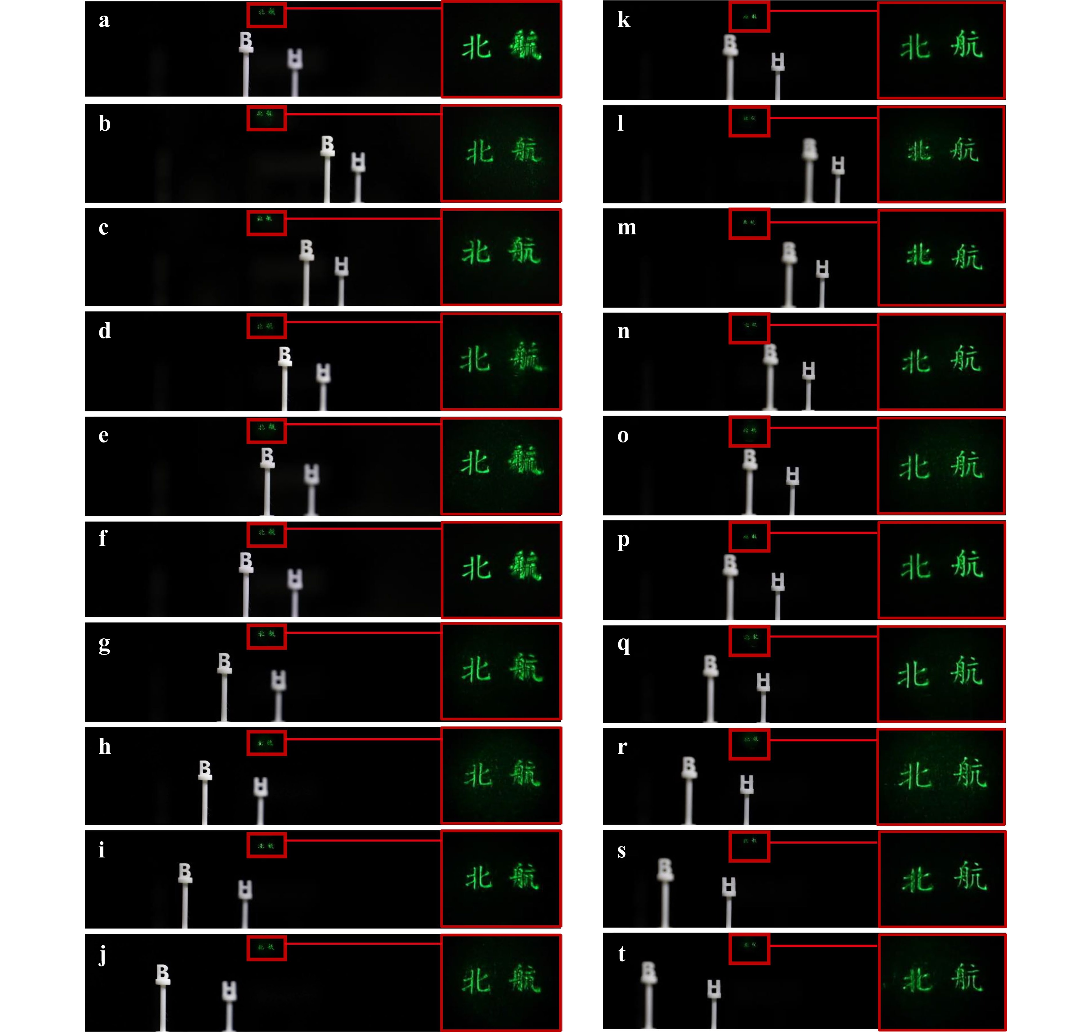
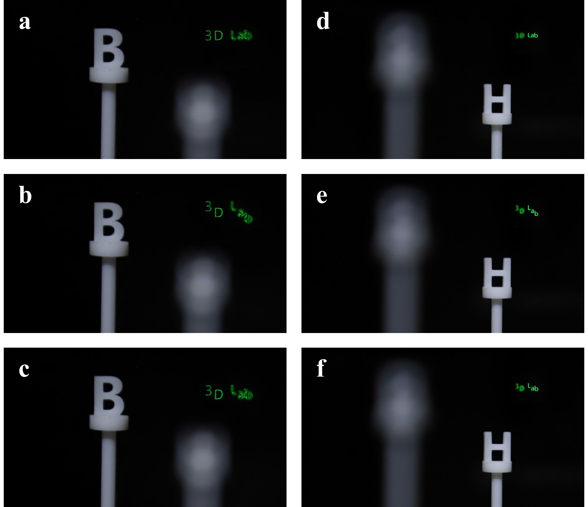
An ideal holographic 3D display should have the characteristics of large viewing angle, full color, and low speckle noise. However, the viewing angle of the holographic 3D display is usually limited by existing strategies, which vastly hinders its extensive application. In this paper, a large viewing angle holographic 3D display system based on maximum diffraction modulation is proposed. The core of the proposed system comprises the spatial light modulators (SLMs) and liquid crystal grating. We also present a new feasible scheme for the realization of large viewing angle holographic 3D display. This is achieved by considering the maximum diffraction angle of SLM as the limited diffraction modulation range of each image point. By doing so, we could not only give access to the maximum hologram size of the object, but also tune the reconstructed image of secondary diffraction by using a self-engineered liquid crystal grating. More importantly, the proposed maximum diffraction modulation scheme enables the viewing angle of the proposed system to be enlarged to 73.4°. The proposed system has huge application potential in the fields such as education, culture, and entertainment.
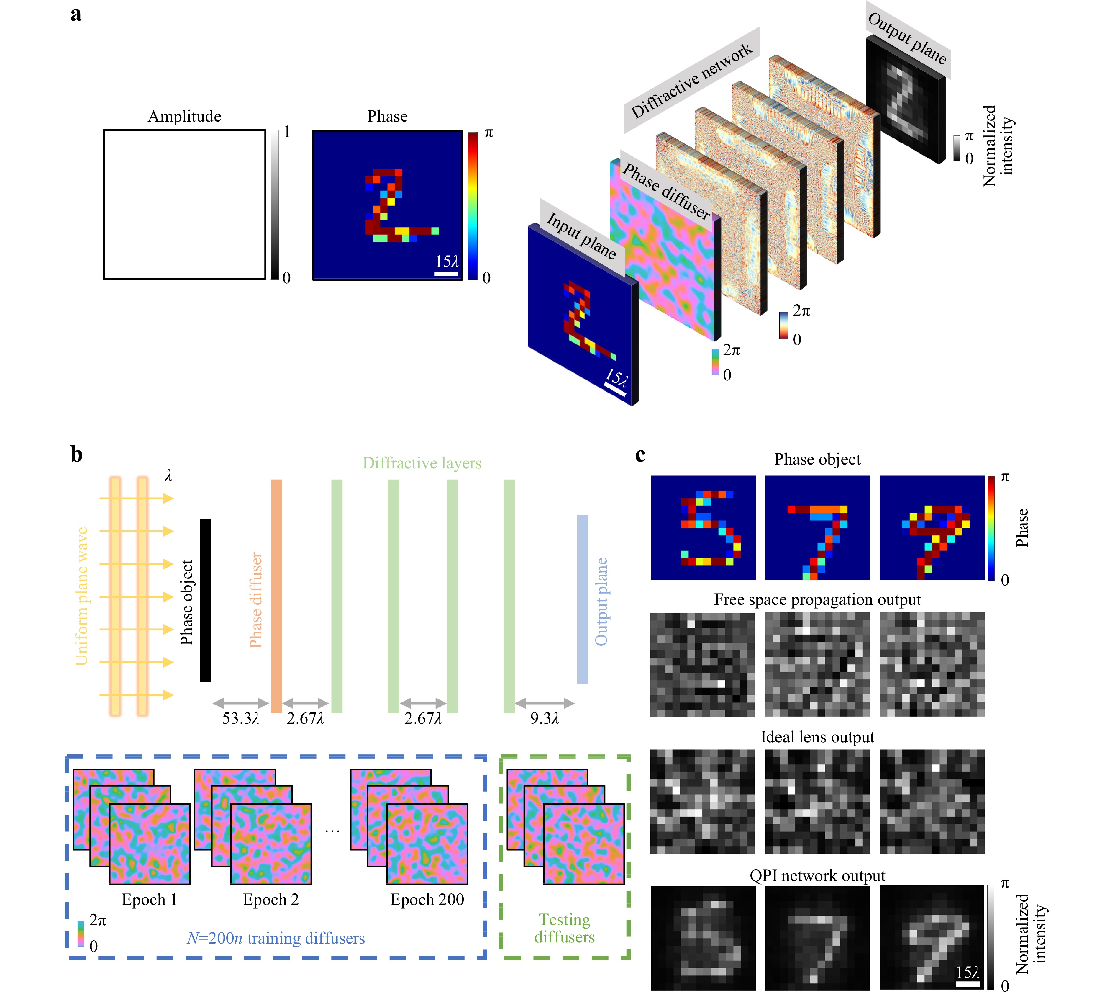
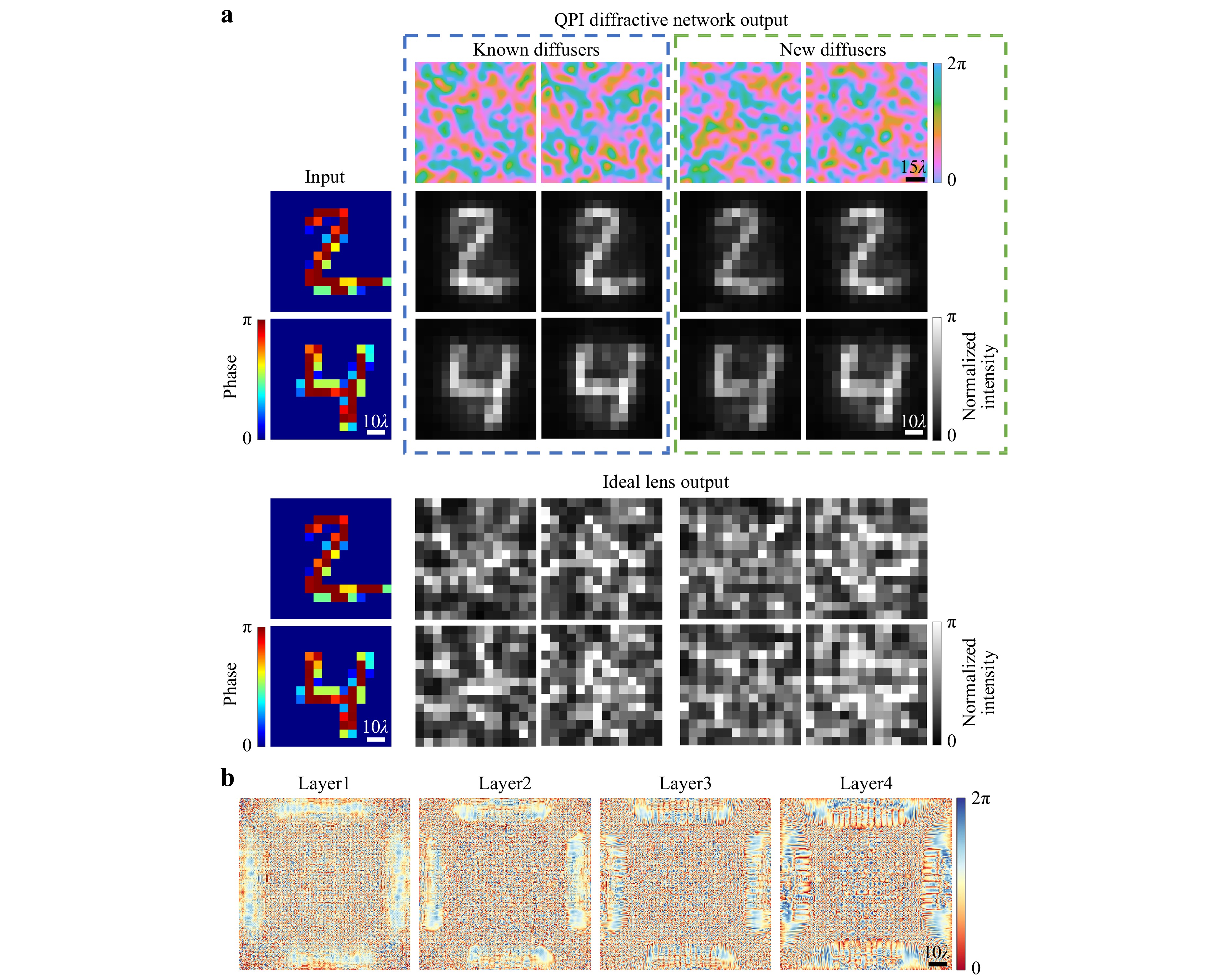
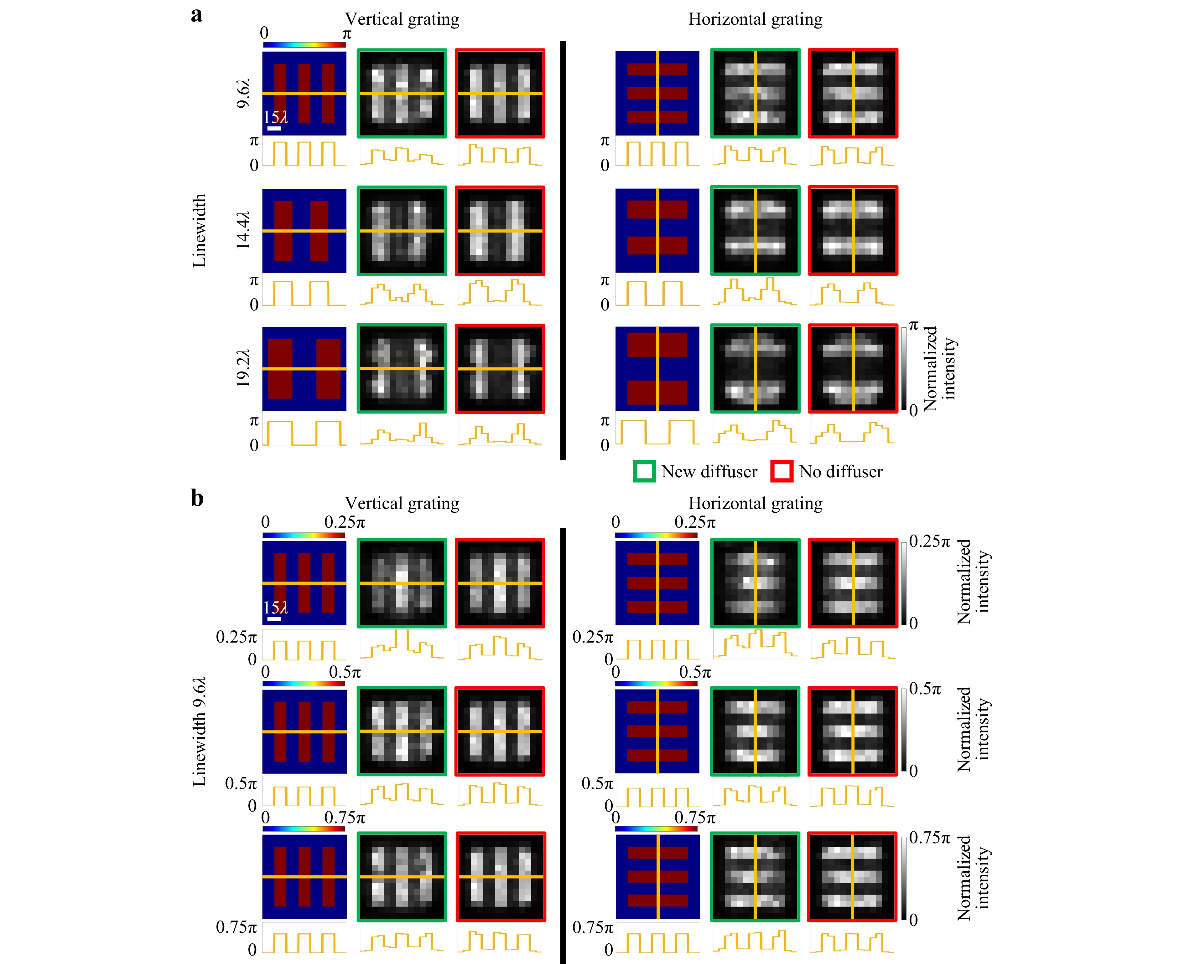
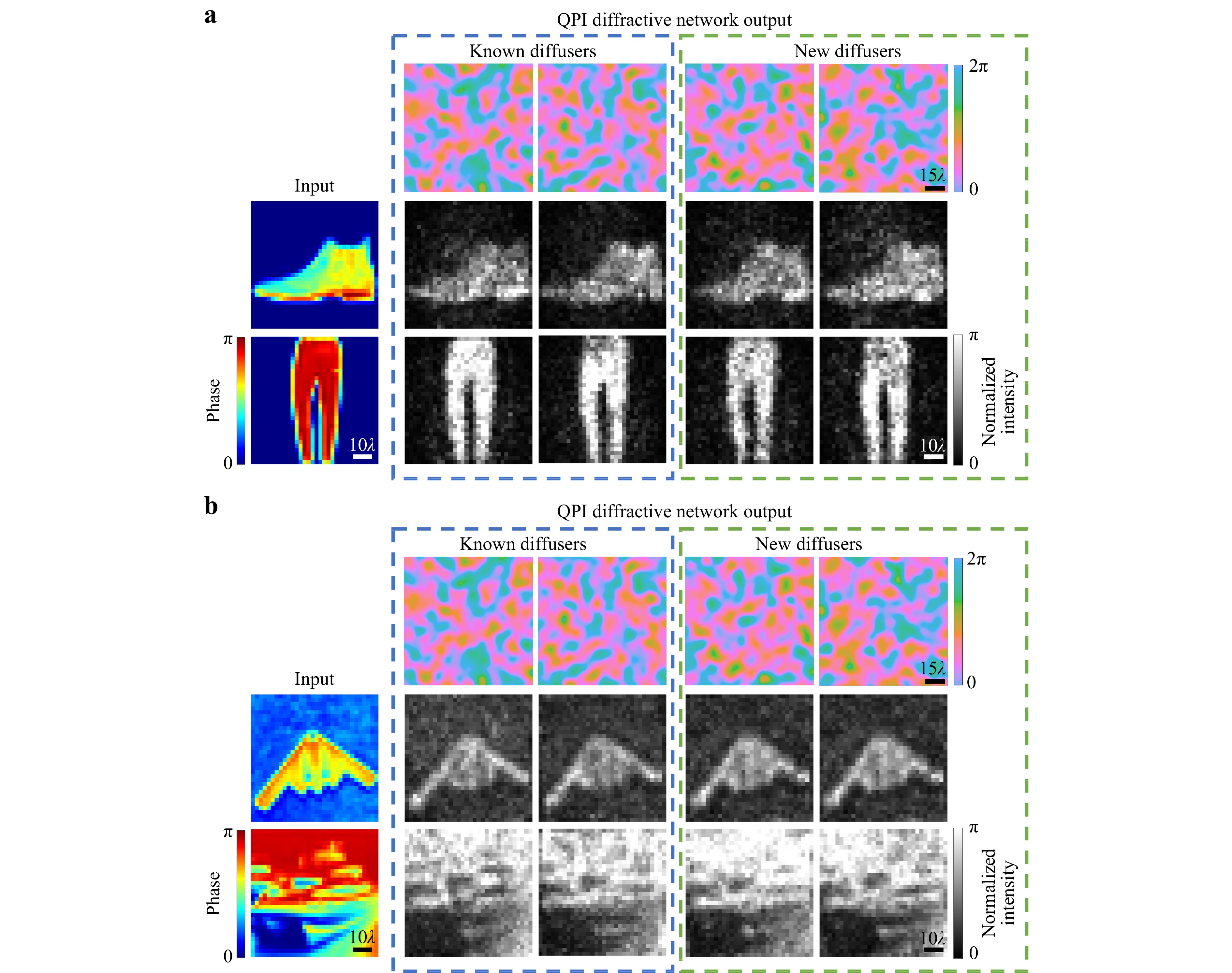
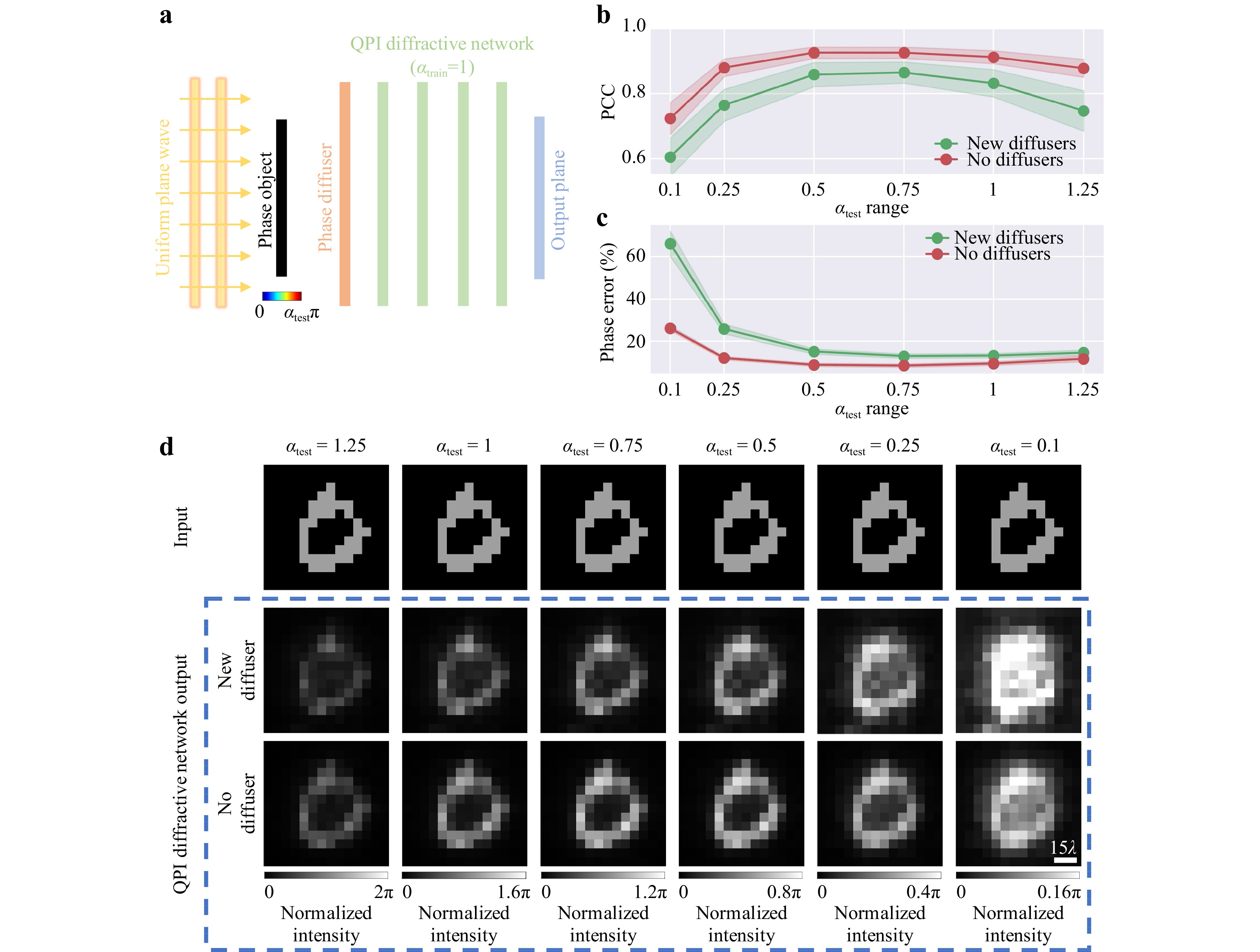
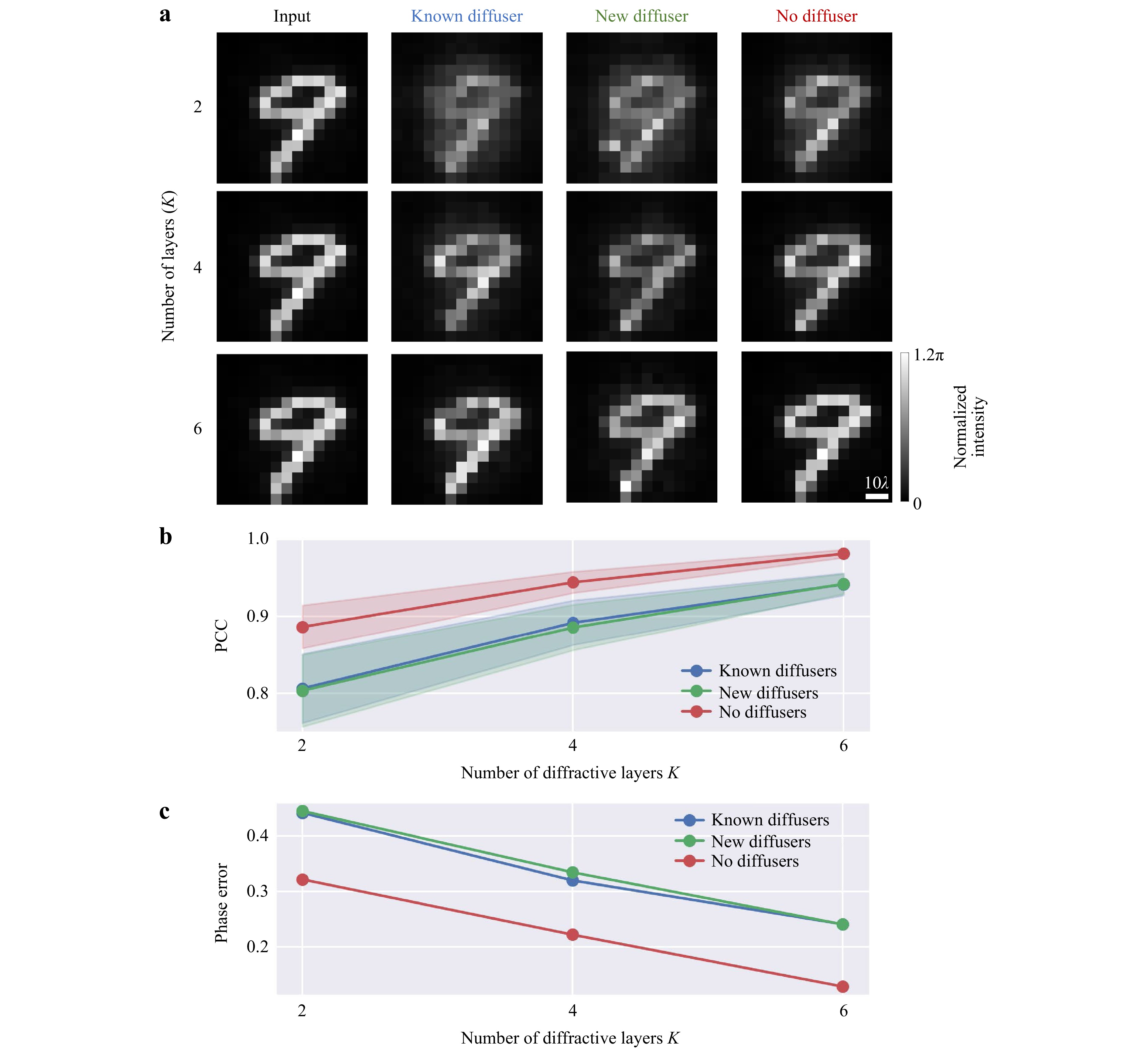
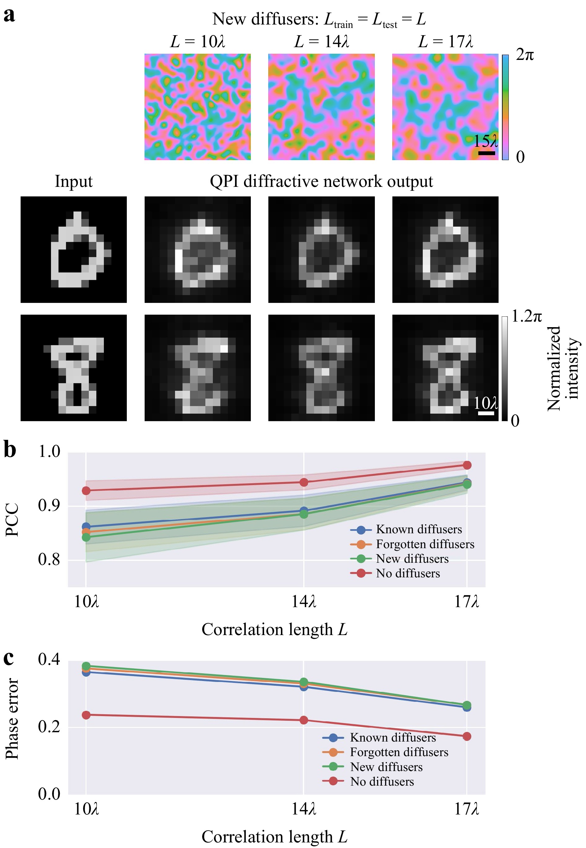
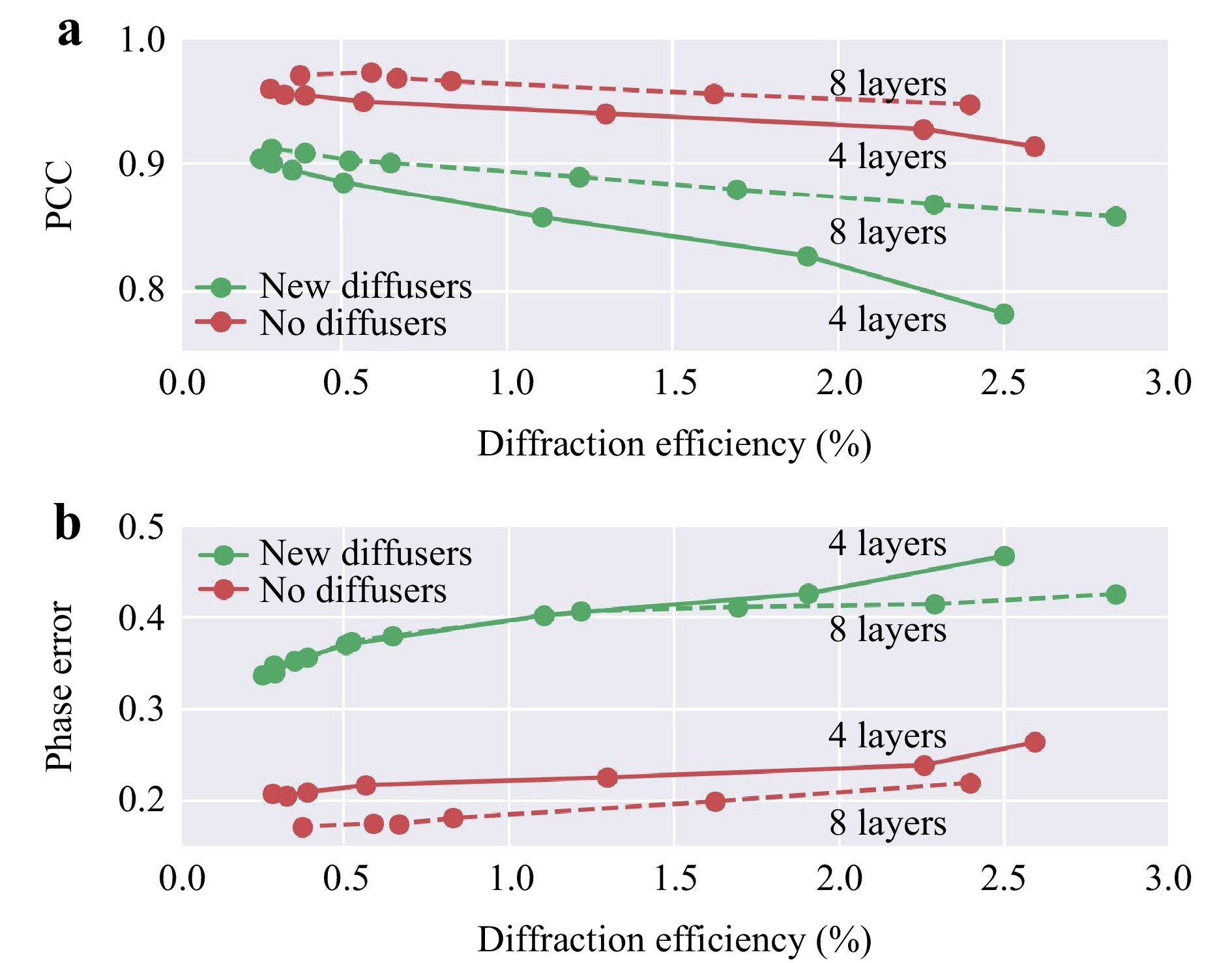
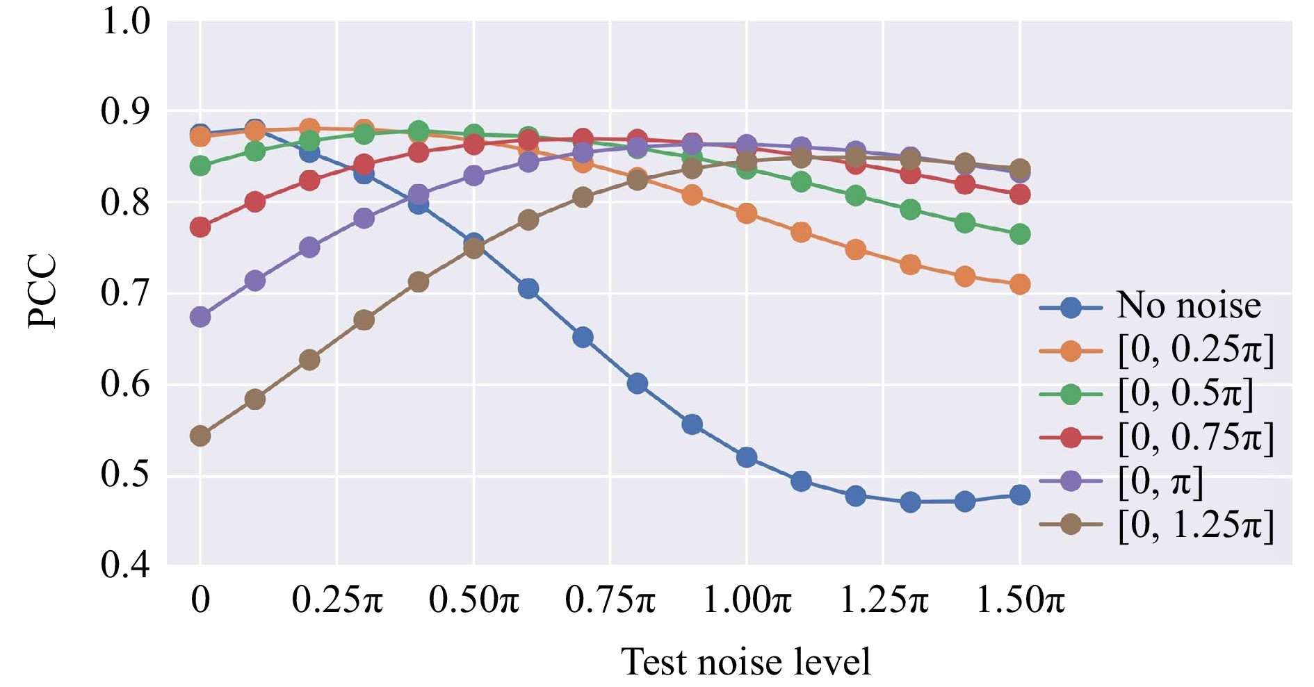
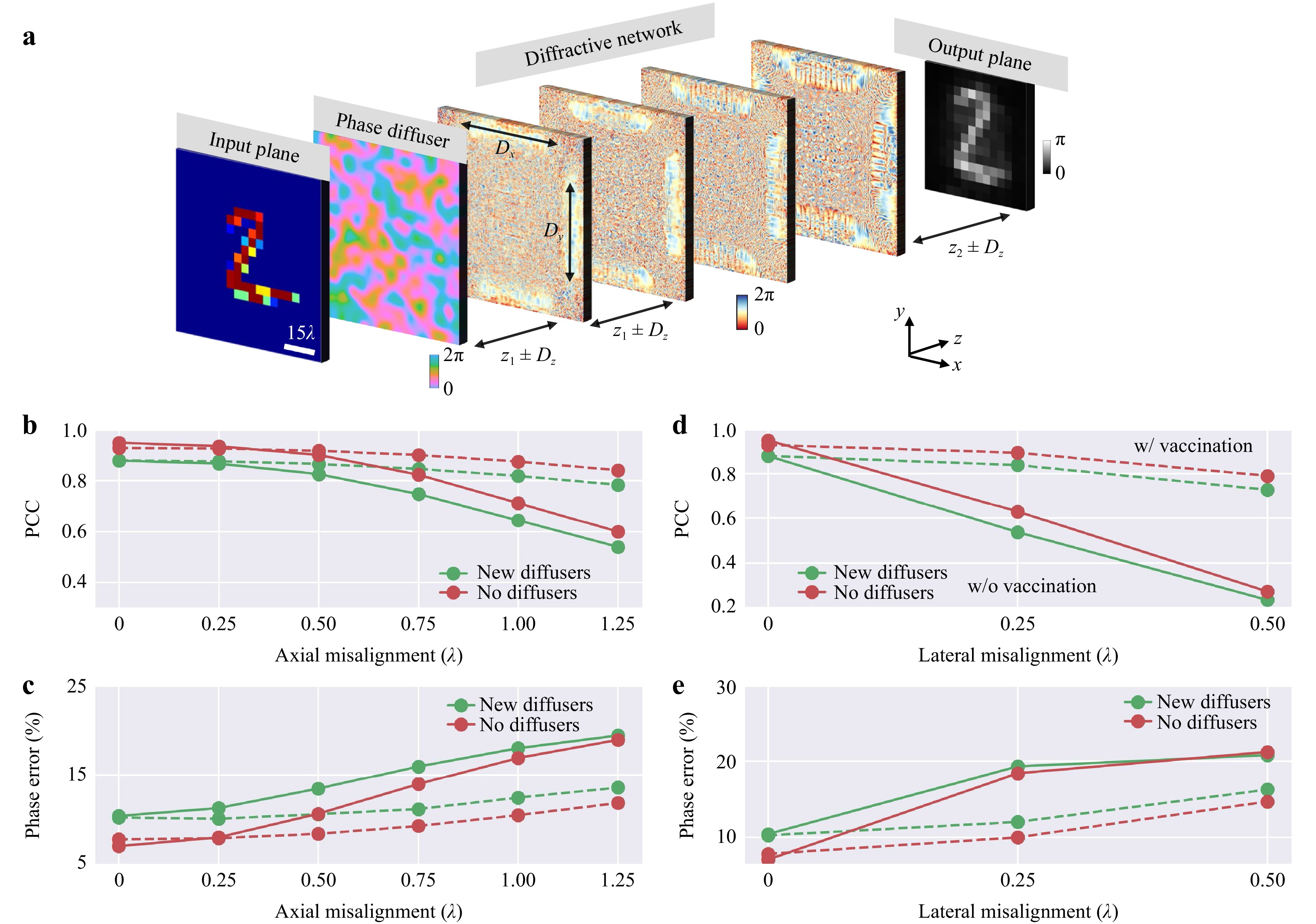
Quantitative phase imaging (QPI) is a label-free computational imaging technique used in various fields, including biology and medical research. Modern QPI systems typically rely on digital processing using iterative algorithms for phase retrieval and image reconstruction. Here, we report a diffractive optical network trained to convert the phase information of input objects positioned behind random diffusers into intensity variations at the output plane, all-optically performing phase recovery and quantitative imaging of phase objects completely hidden by unknown, random phase diffusers. This QPI diffractive network is composed of successive diffractive layers, axially spanning in total ~70
, where
is the illumination wavelength; unlike existing digital image reconstruction and phase retrieval methods, it forms an all-optical processor that does not require external power beyond the illumination beam to complete its QPI reconstruction at the speed of light propagation. This all-optical diffractive processor can provide a low-power, high frame rate and compact alternative for quantitative imaging of phase objects through random, unknown diffusers and can operate at different parts of the electromagnetic spectrum for various applications in biomedical imaging and sensing. The presented QPI diffractive designs can be integrated onto the active area of standard CCD/CMOS-based image sensors to convert an existing optical microscope into a diffractive QPI microscope, performing phase recovery and image reconstruction on a chip through light diffraction within passive structured layers.
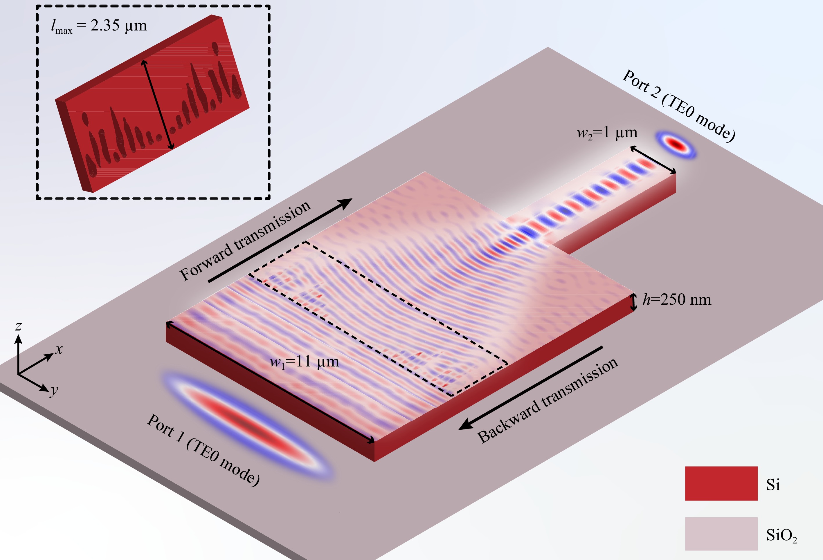
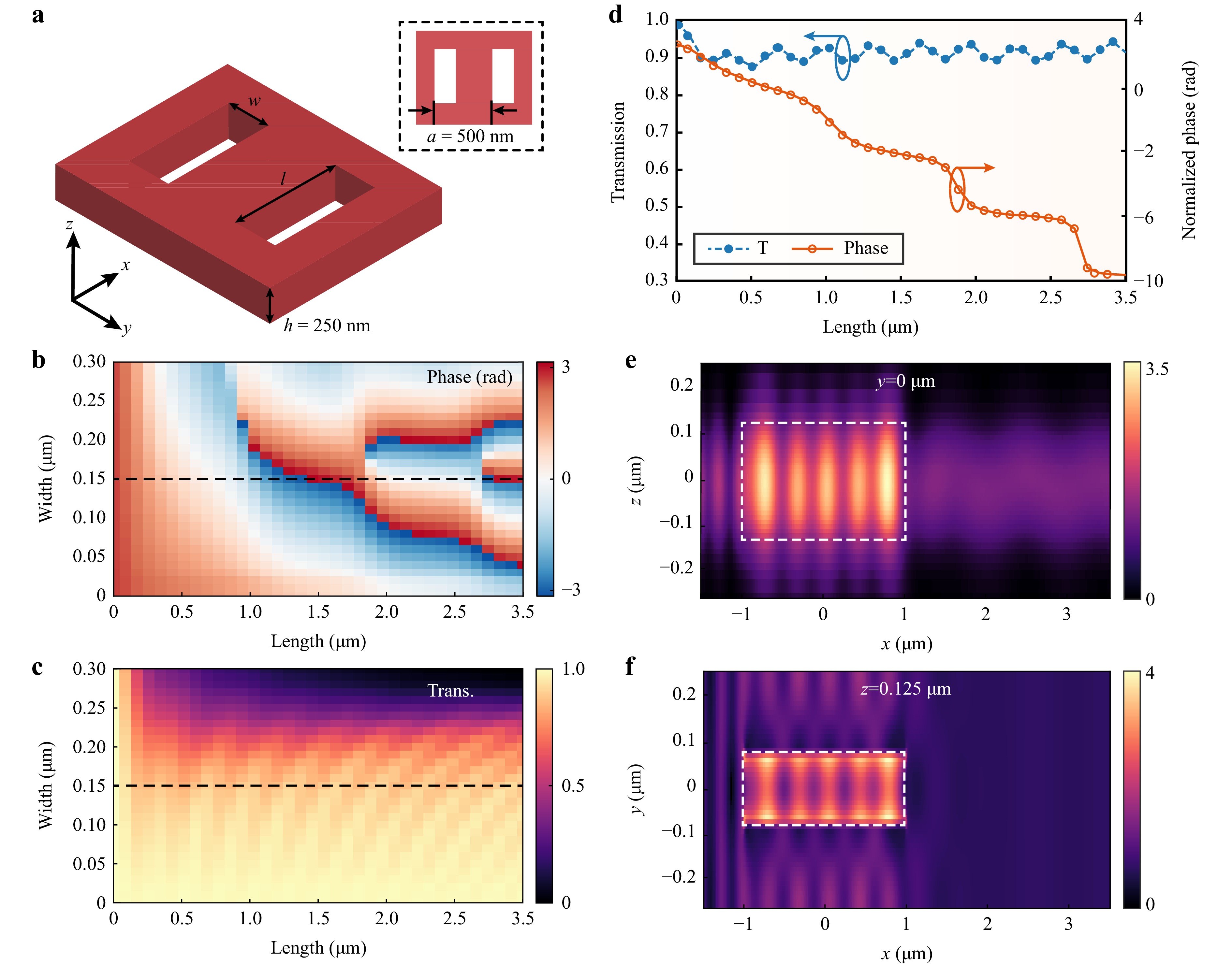
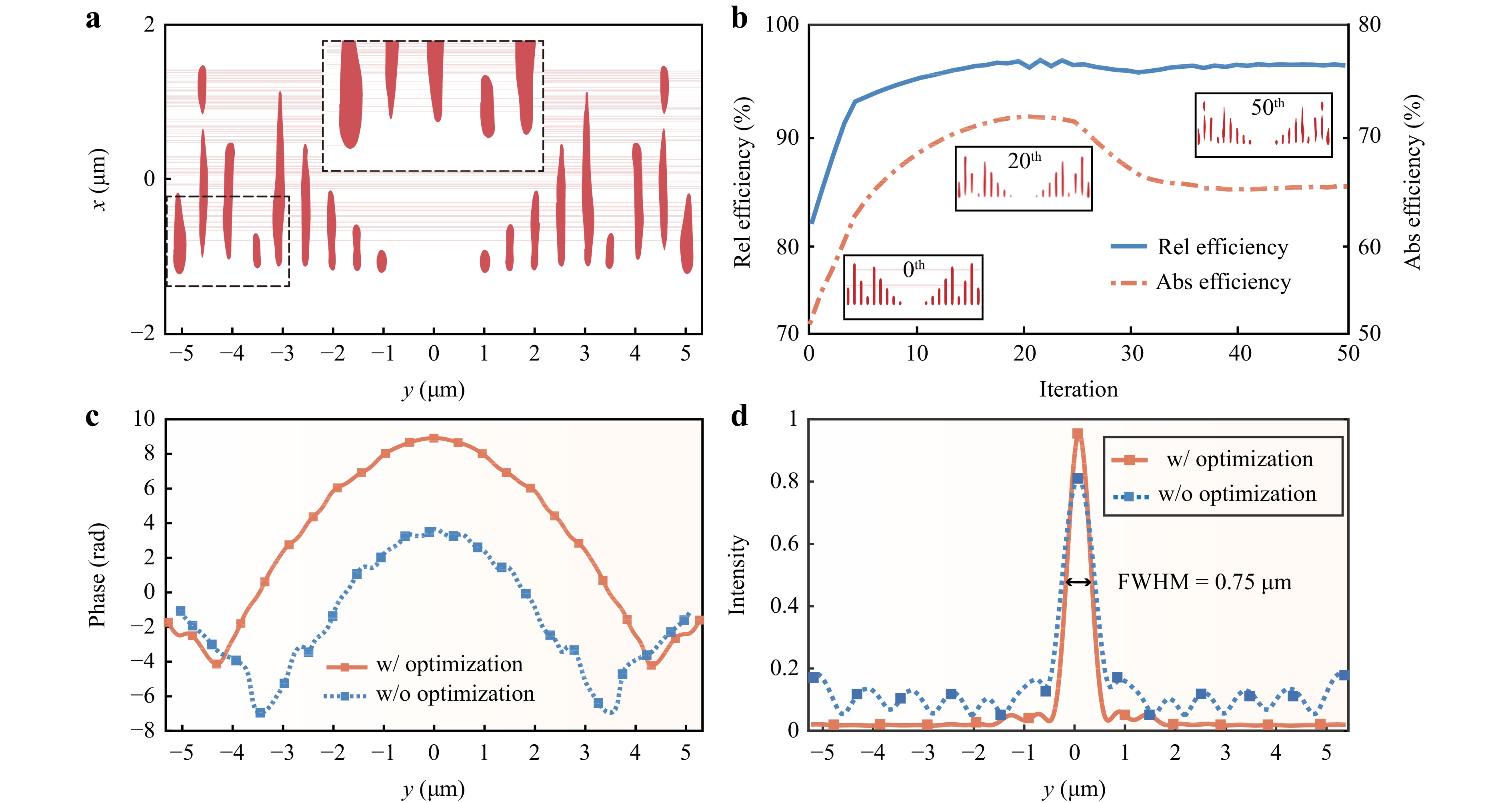
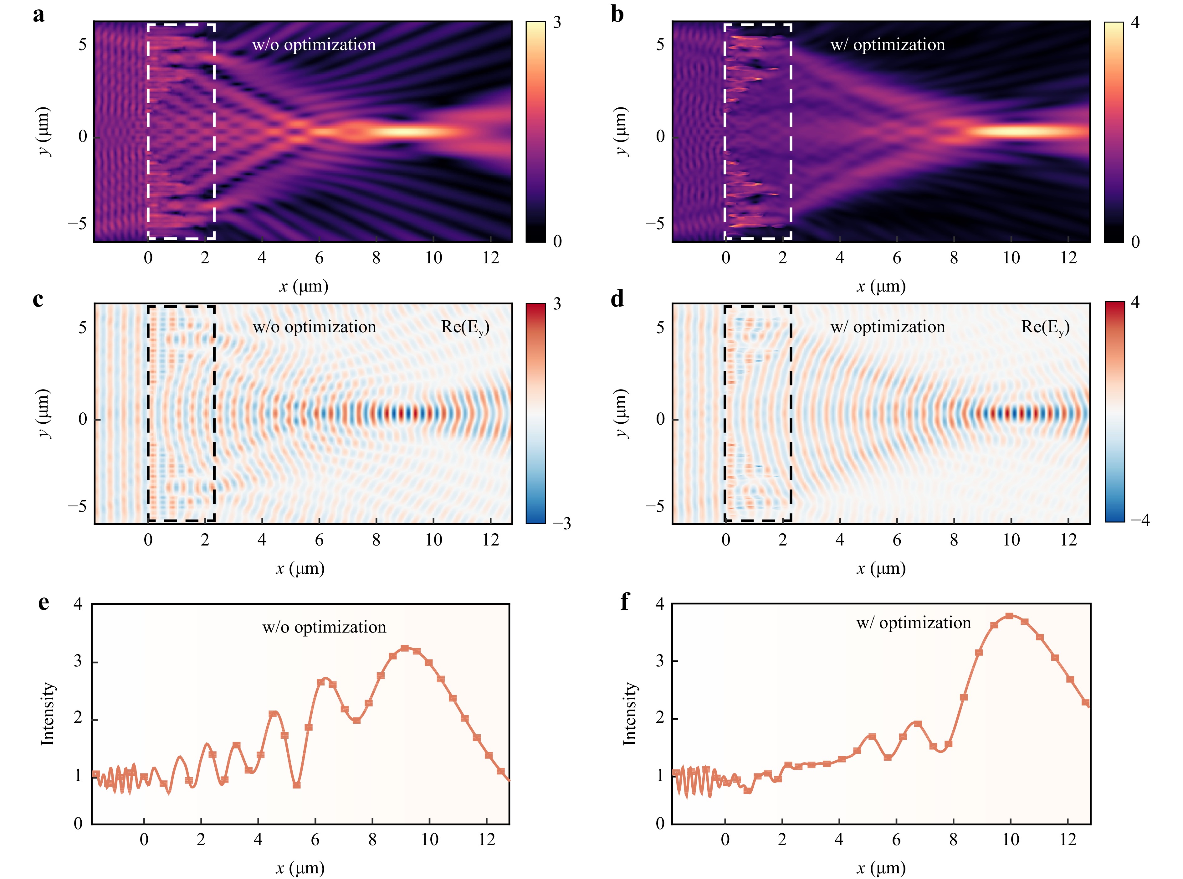
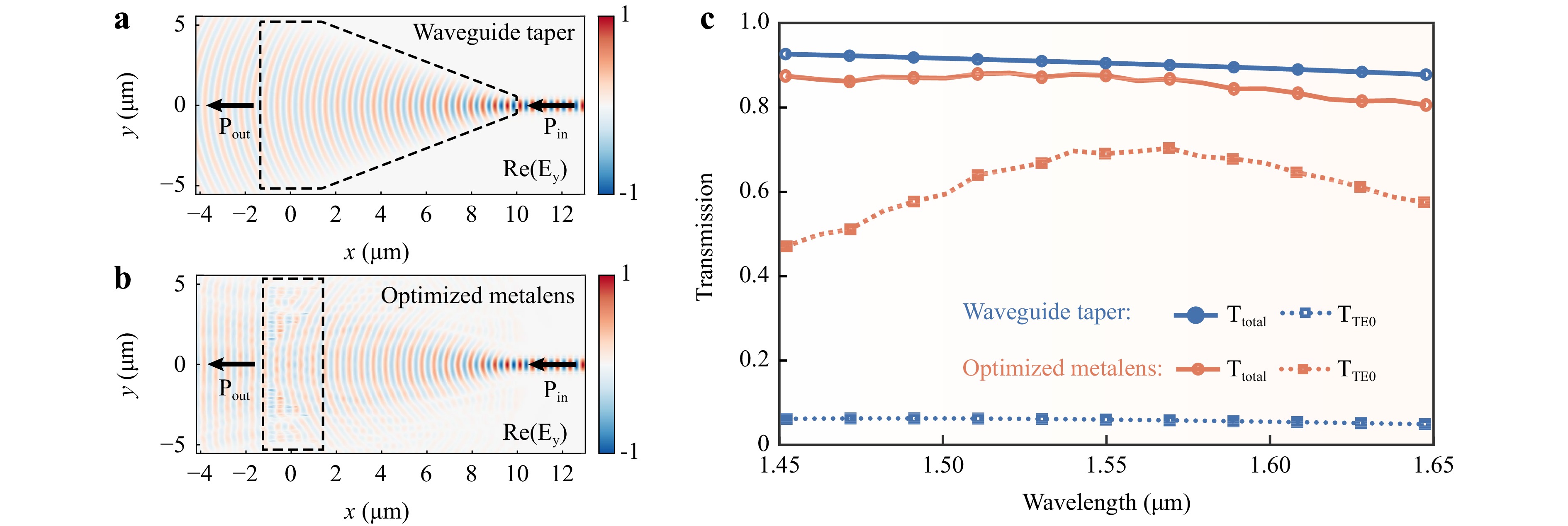
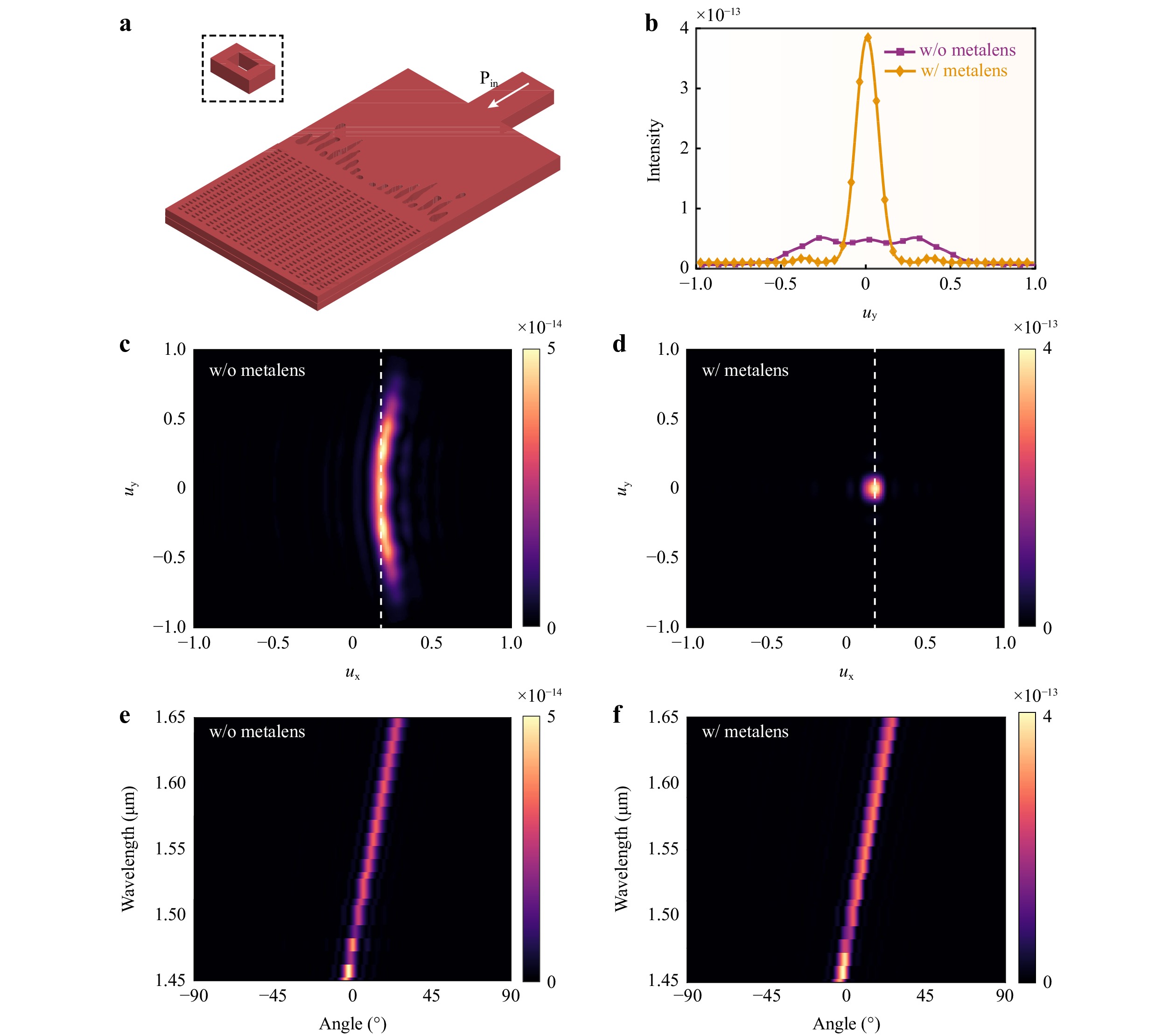
Photonic integrated circuits (PICs) have attracted significant interest in communication, computation, and biomedical applications. However, most rely on highly integrated PICs devices, which require a low-loss and high-integration guided wave path. Owing to the various dimensions of different integrated photonic devices, their interconnections typically require waveguide tapers. Although a waveguide taper can overcome the width mismatch of different devices, its inherent tapering width typically results in a long length, which fundamentally limits the efficient interconnection between devices with a high scaling ratio over a short distance. Herein, we proposed a highly integrated on-chip metalens that enables optical interconnections between devices with high width-scaling ratios by embedding a free-form metasurface in a silicon-on-insulator film. The special geometric features endow the designed metalens with high coupling efficiency and high integration. The device has a footprint of only 2.35 μm in the longitudinal direction and numerical aperture of 2.03, enabling beam focusing and collimation of less than 10 μm between devices with width-scaling ratio of 11. For the fundamental transverse electric field (TE0) mode, the relative transmittance is as high as 96% for forward incidence (from wide to narrow waveguides), whereas the metalens can realize wavefront shaping for backward incidence, which can be used in optical phase arrays. This study provides new ideas for optical interconnect design and wavefront shaping in high-integration PICs. Our design approach has potential applications in directional radiators, LiDAR, on-chip optical information processing, analogue computing, and imaging.
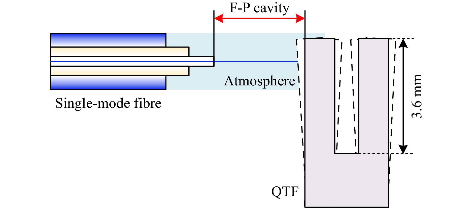
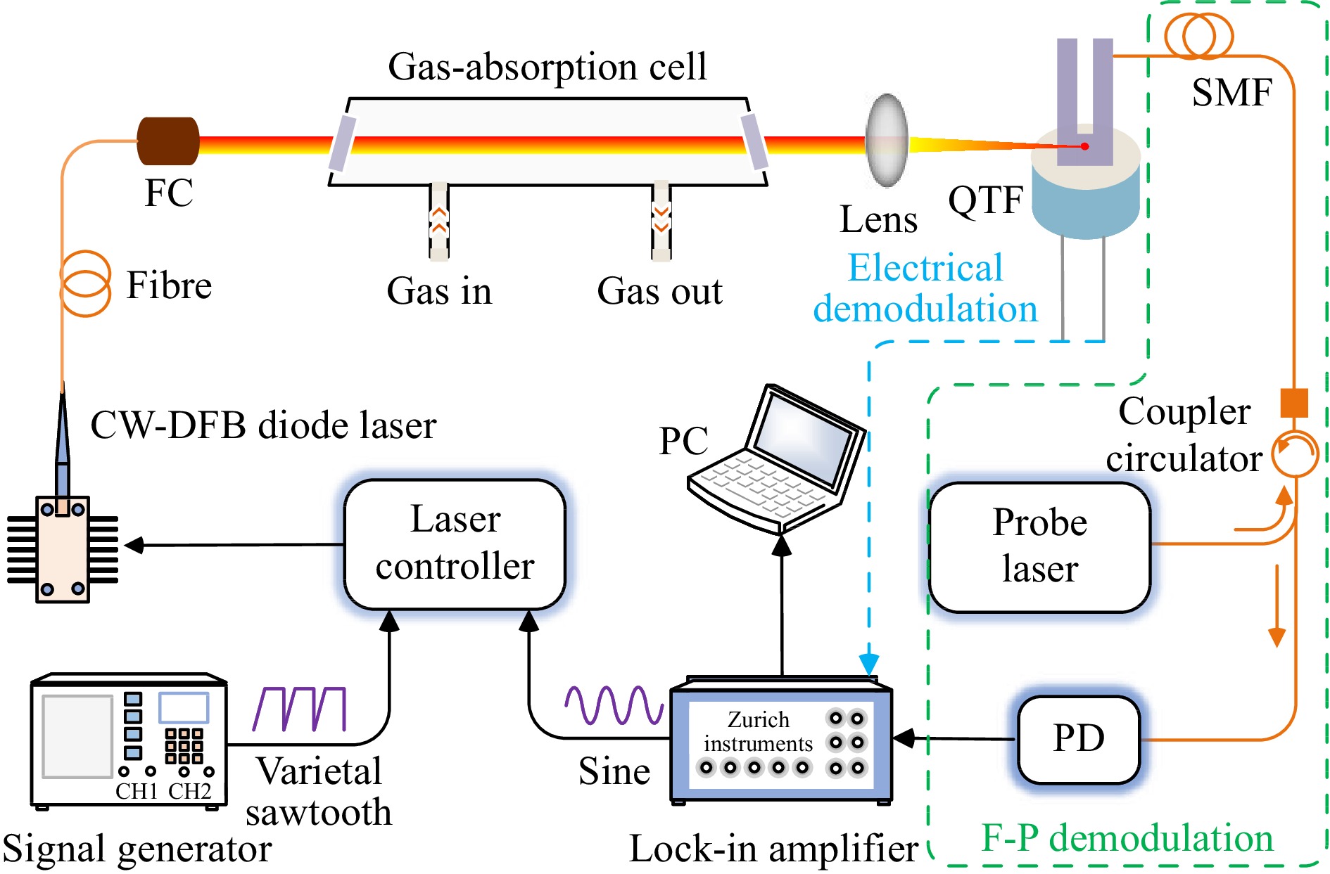
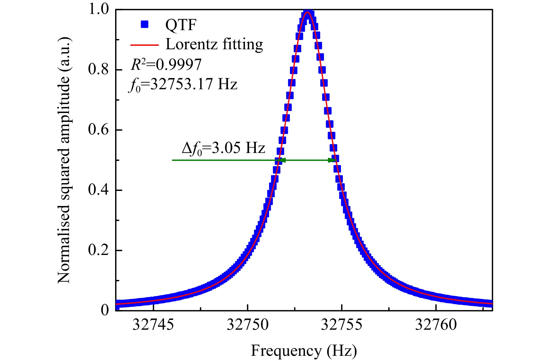
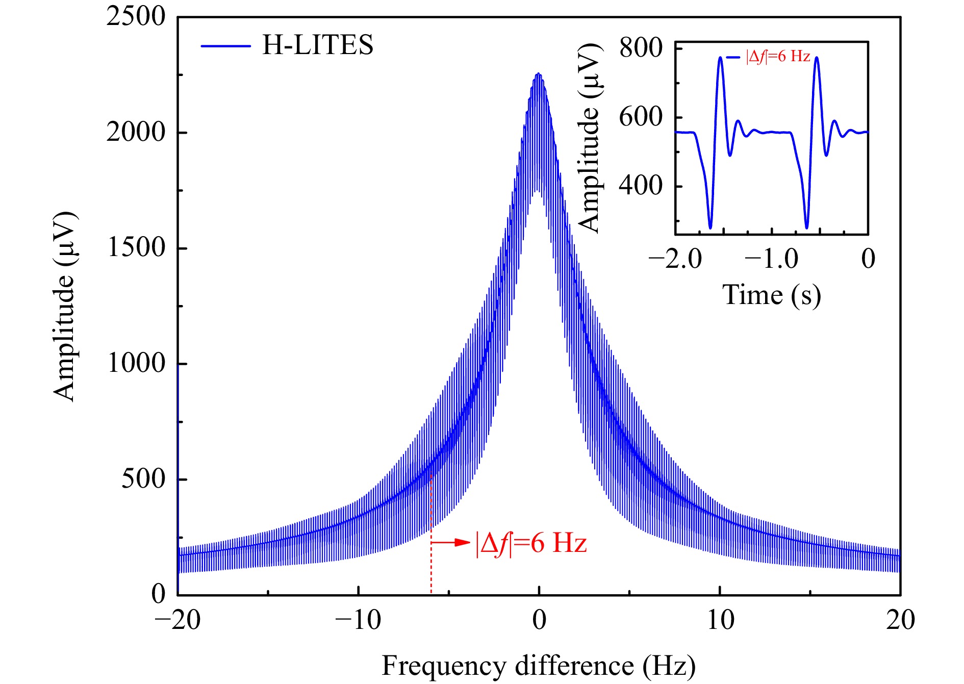
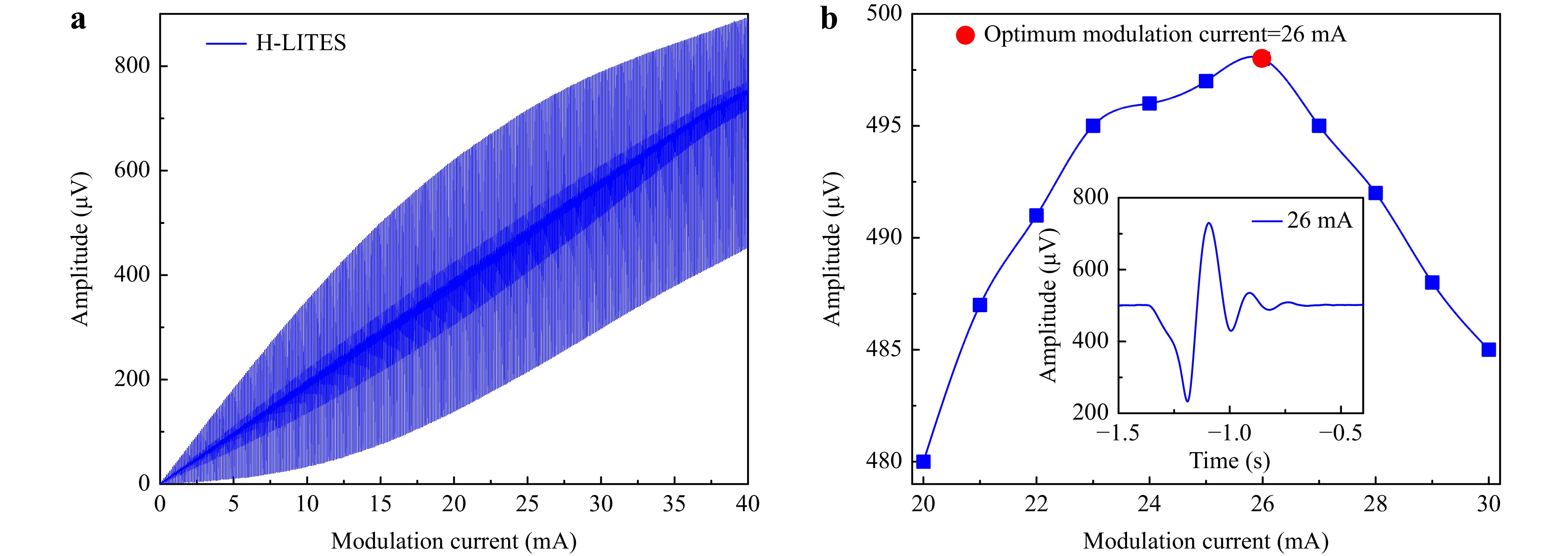
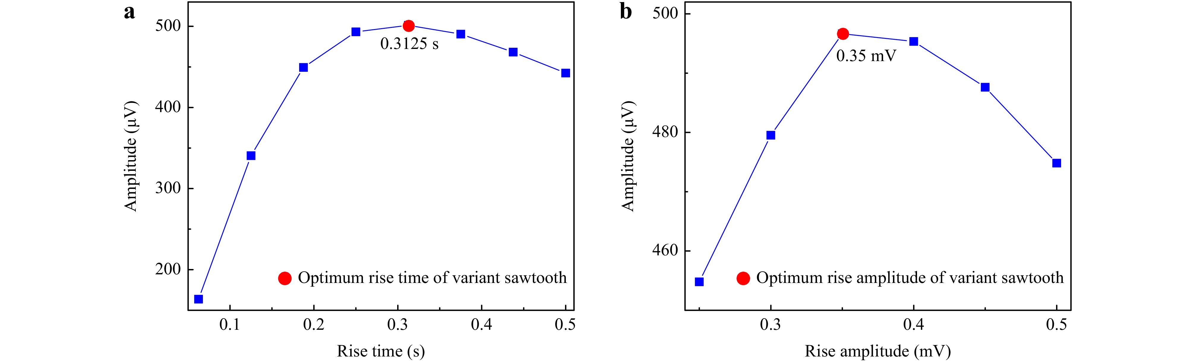
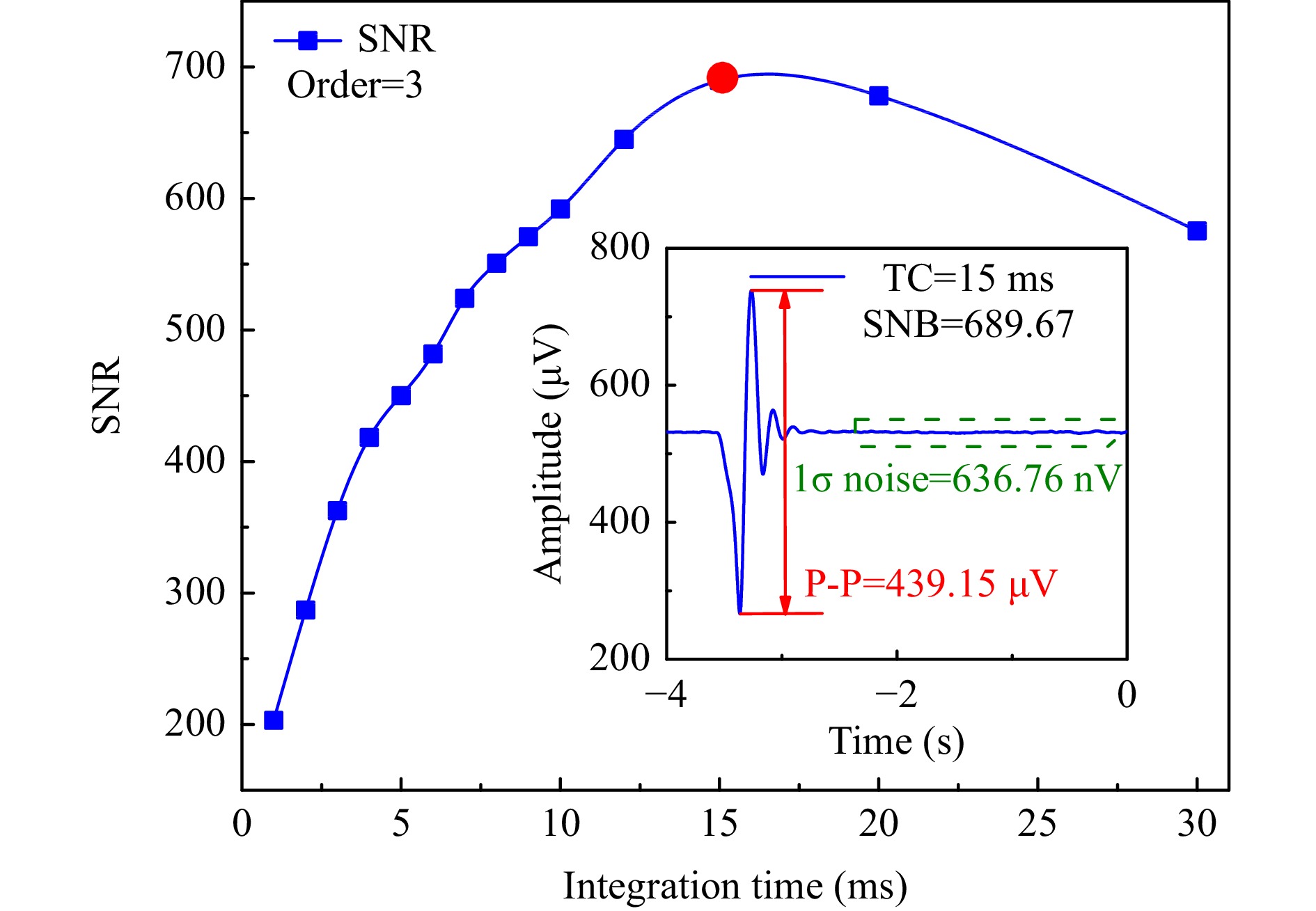
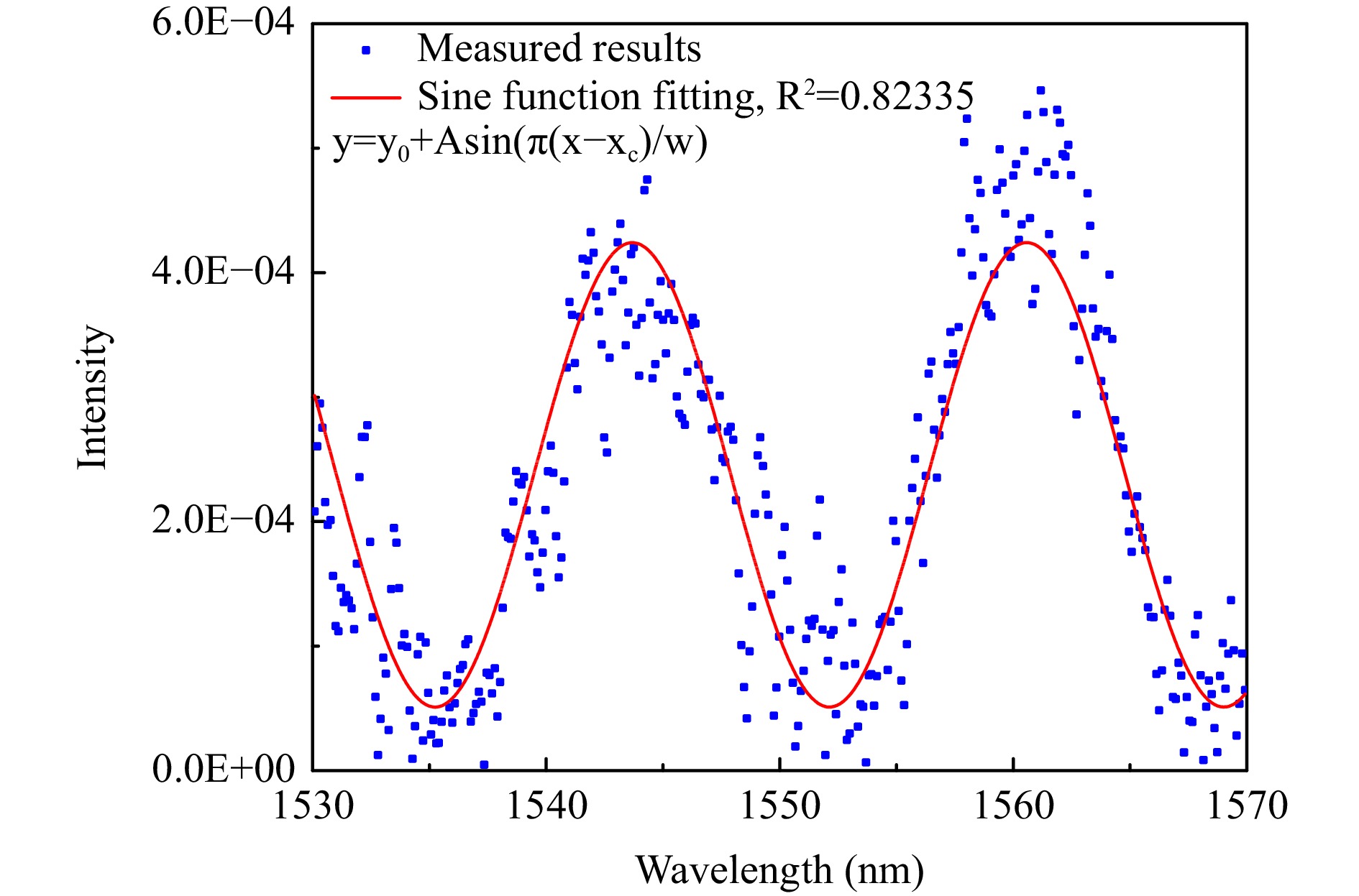
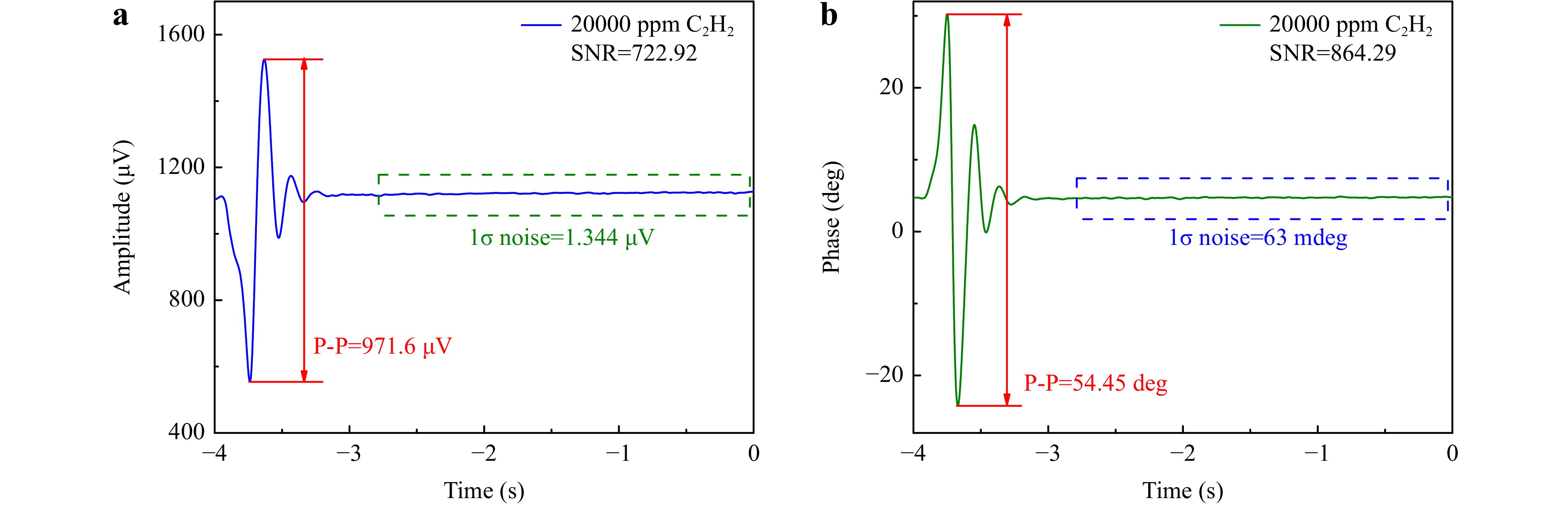
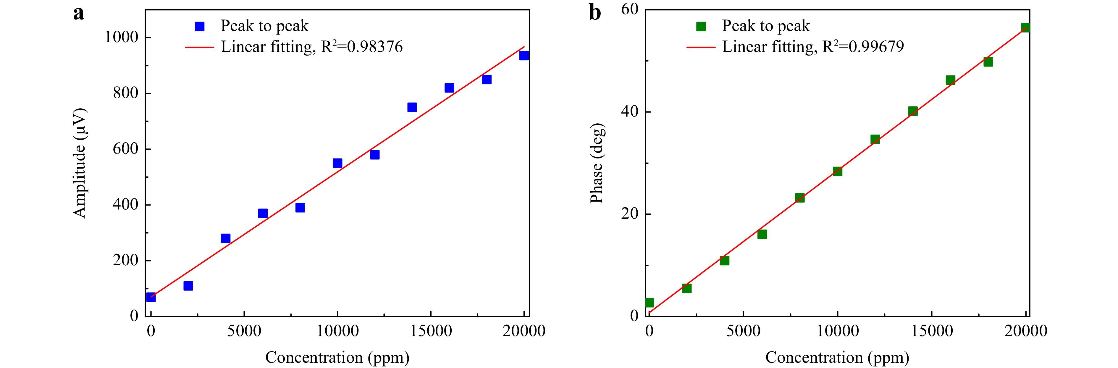
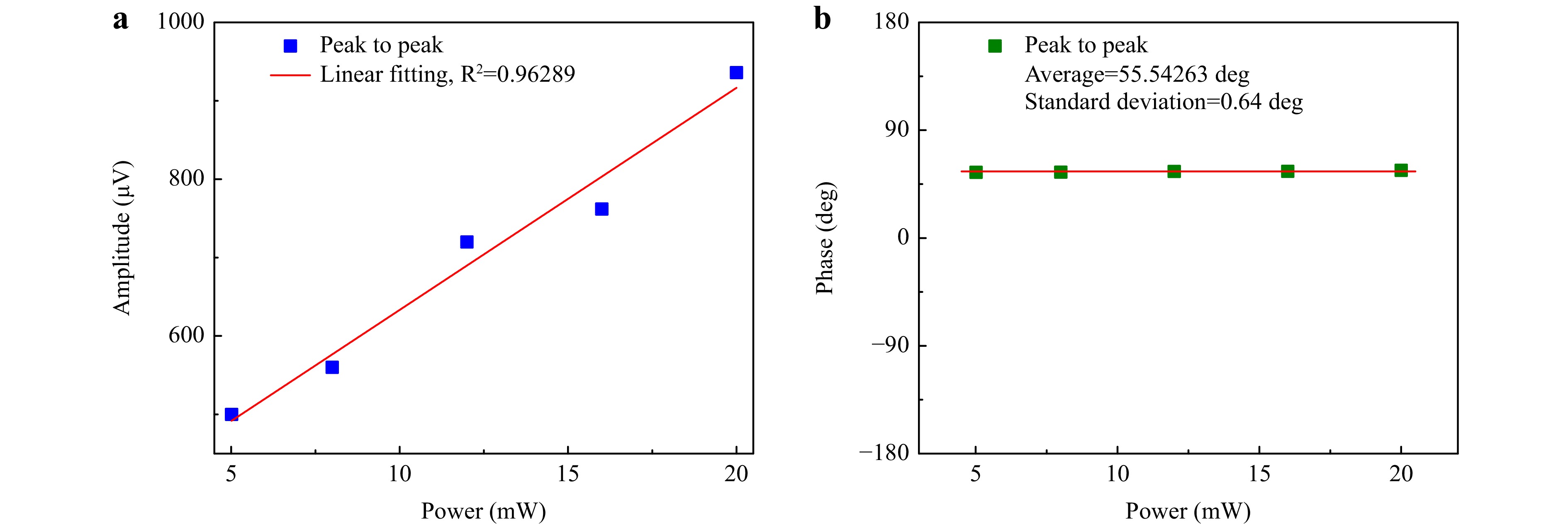
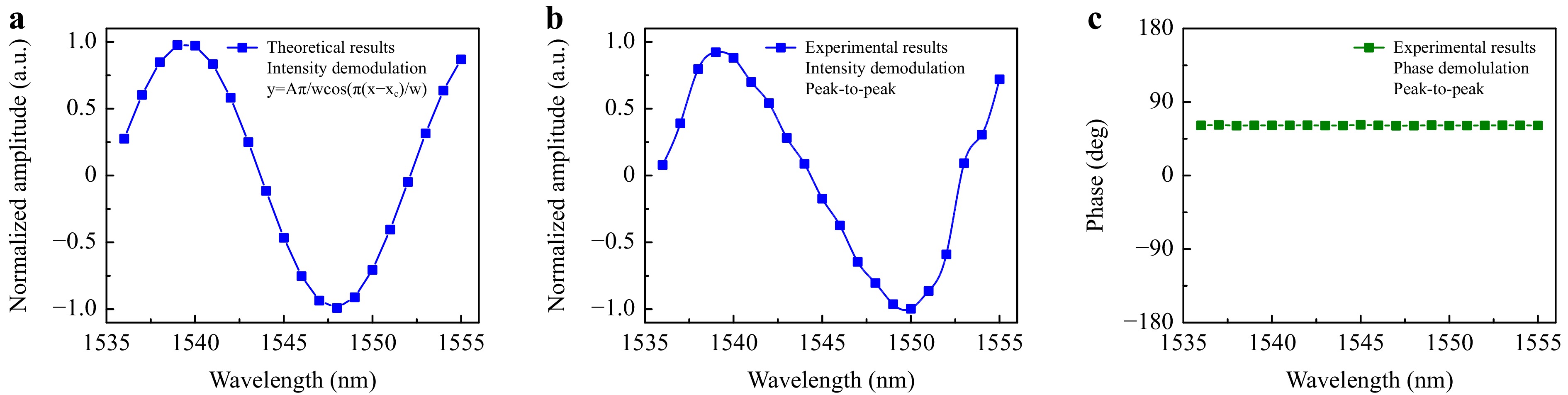
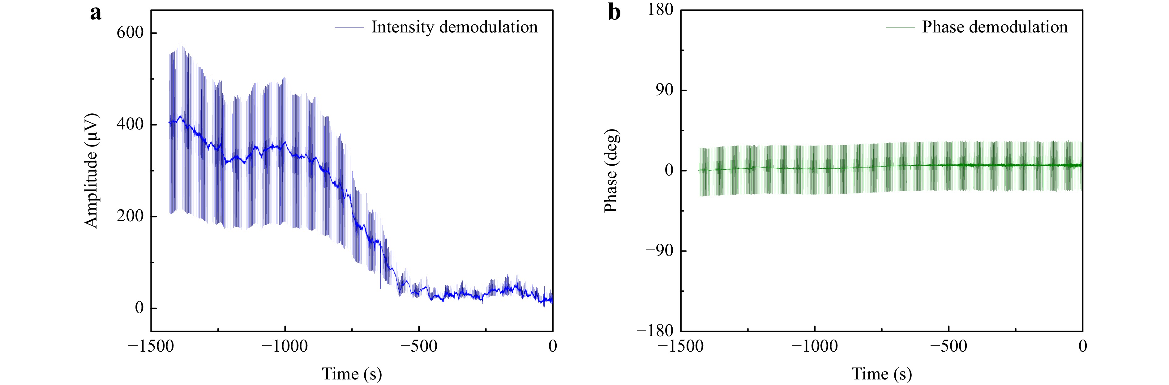
Fabry–Perot (F–P)-based phase demodulation of heterodyne light-induced thermoelastic spectroscopy (H-LITES) was demonstrated for the first time in this study. The vibration of a quartz tuning fork (QTF) was detected using the F–P interference principle instead of an electrical signal through the piezoelectric effect of the QTF in traditional LITES to avoid thermal noise. Given that an Fabry–Perot interferometer (FPI) is vulnerable to disturbances, a phase demodulation method that has been demonstrated theoretically and experimentally to be an effective solution for instability was used in H-LITES. The sensitivity of the F–P phase demodulation method based on the H-LITES sensor was not associated with the wavelength or power of the probe laser. Thus, stabilising the quadrature working point (Q-point) was no longer necessary. This new method of phase demodulation is structurally simple and was found to be resistant to interference from light sources and the surroundings using the LITES technique.
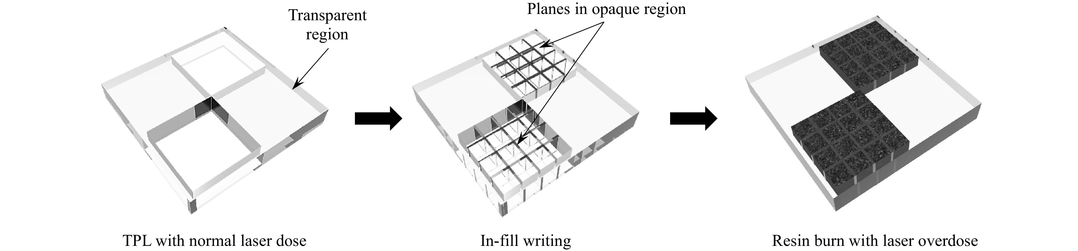
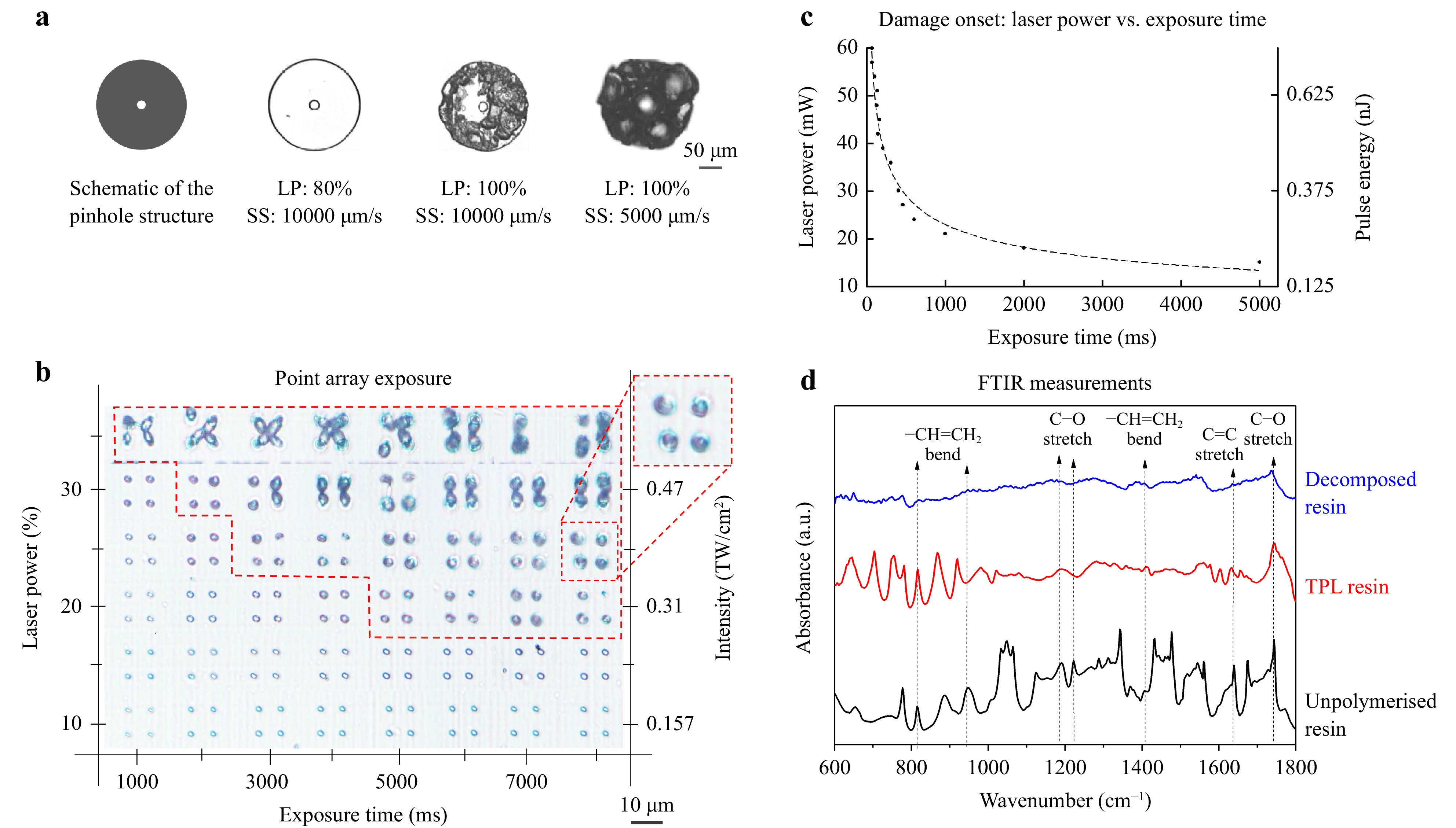
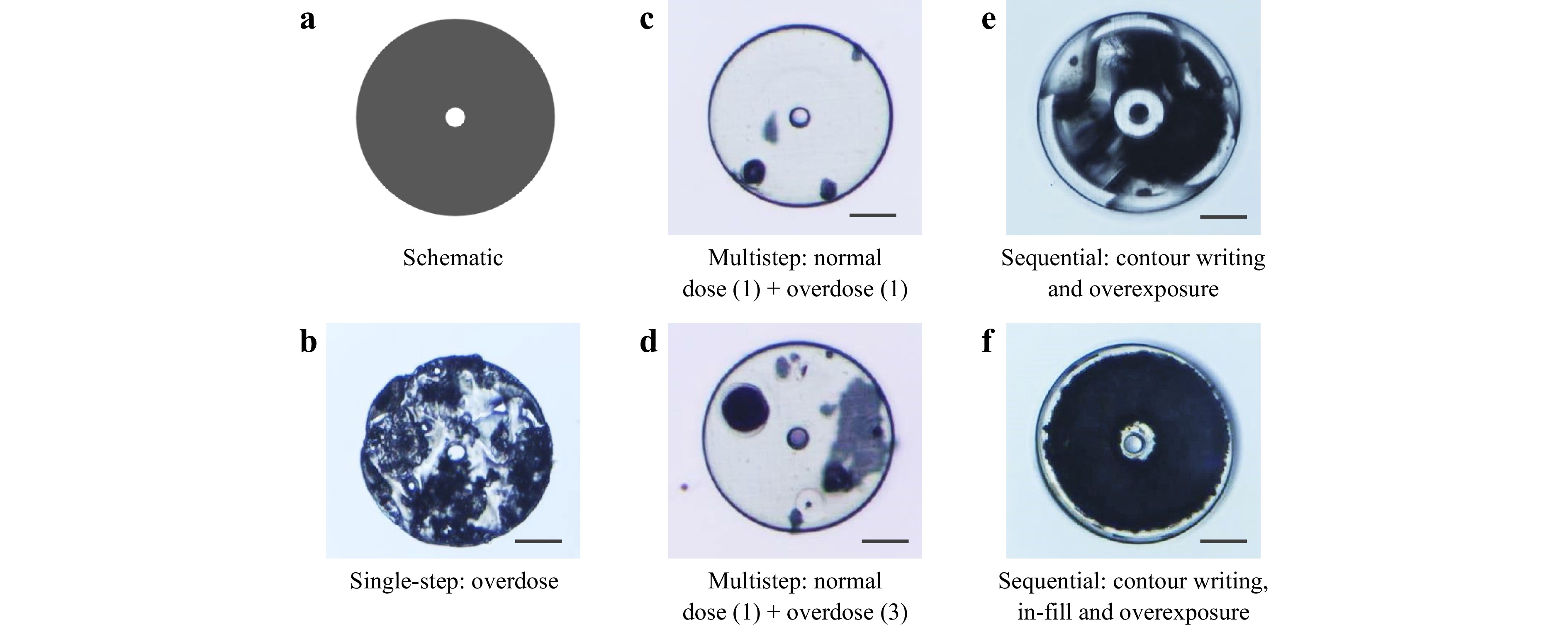
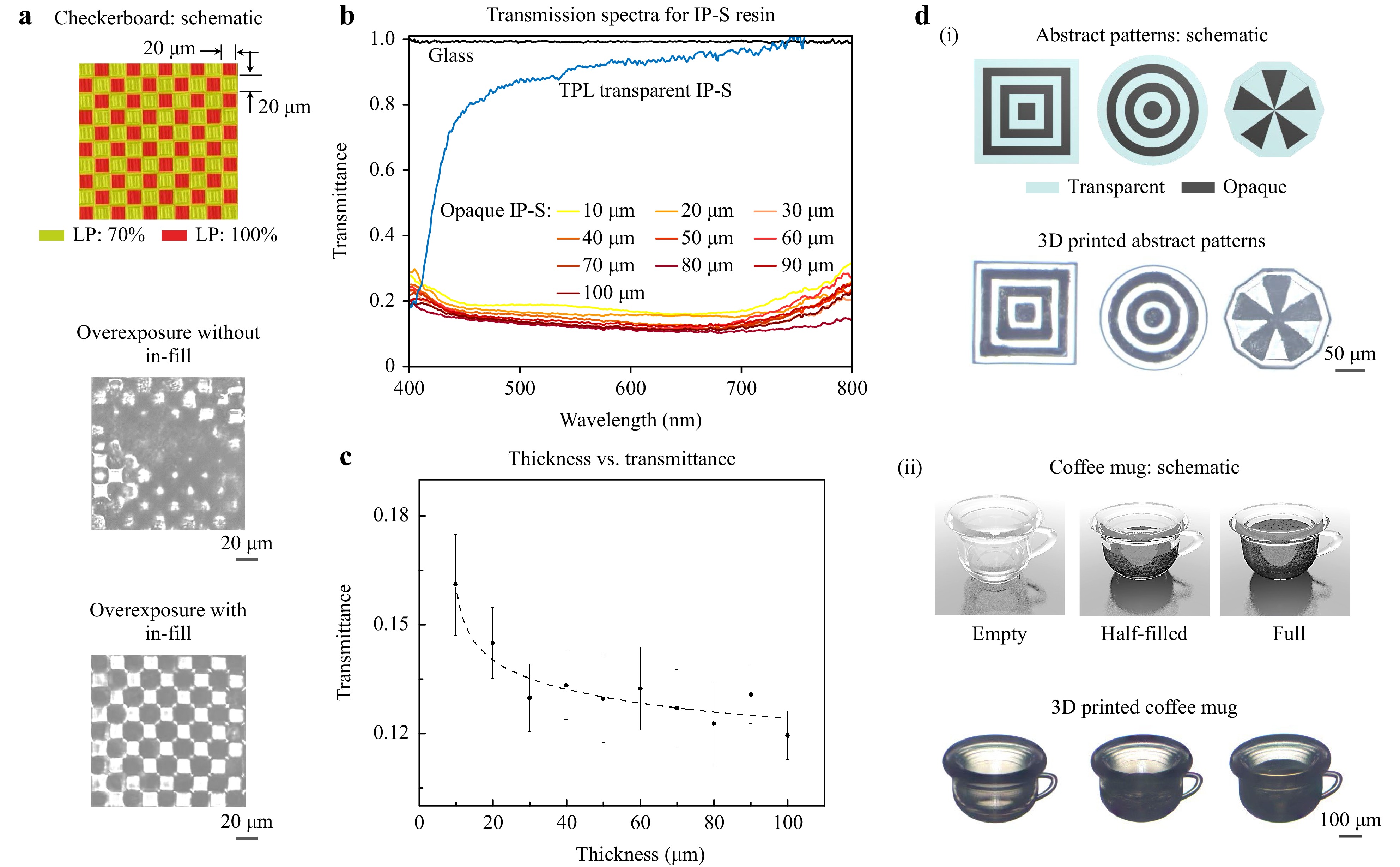
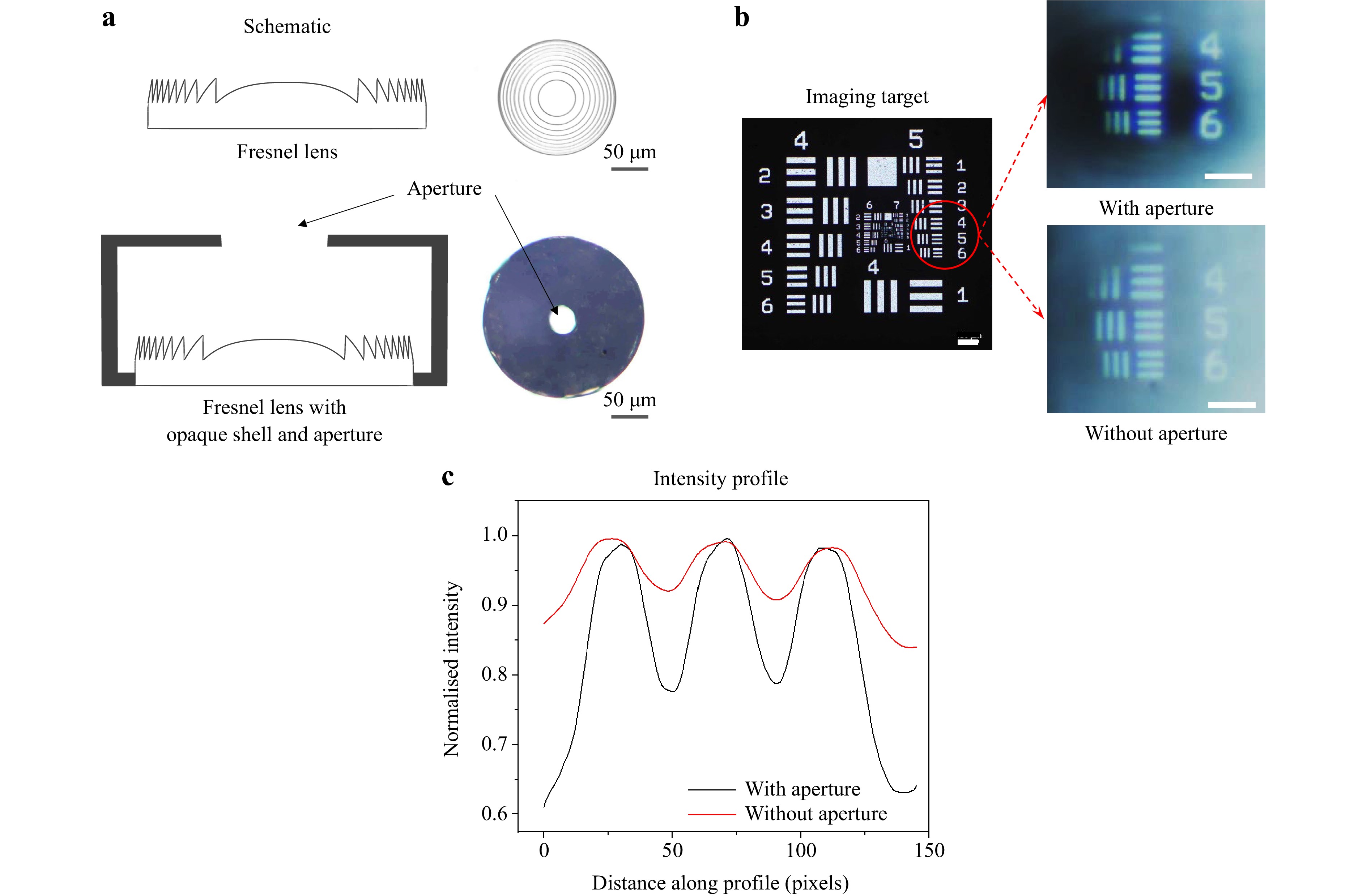
Two-photon polymerisation lithography enables the three-dimensional (3D)-printing of high-resolution micron- and nano-scale structures. Structures that are 3D-printed using proprietary resins are transparent and are suitable as optical components. However, achieving a mix of opaque and transparent structures in a single optical component is challenging and requires multiple material systems or the manual introduction of ink after fabrication. In this study, we investigated an overexposure printing process for laser decomposition, which typically produces uncontrollable and random ‘burnt’ structures. Specifically, we present a printing strategy to control this decomposition process, realising the on-demand printing of opaque or transparent structures in a single lithographic step using a single resin. Using this method, opaque structures can be printed with a minimum feature size of approximately 10 µm, which exhibit<15% transmittance at a thickness of approximately 30 µm. We applied this process to print an opaque aperture integrated with a transparent lens to demonstrate an improved imaging contrast.
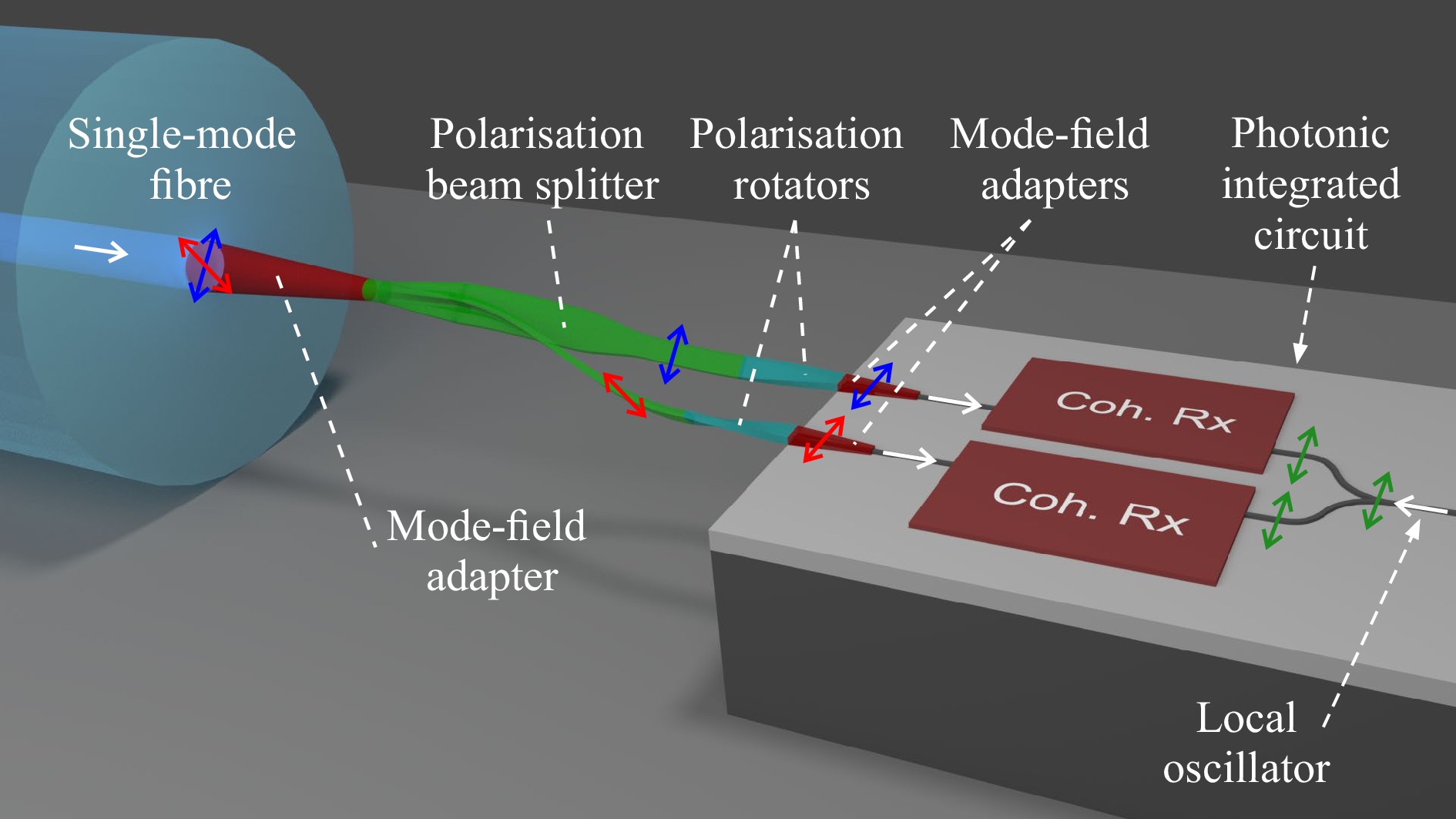
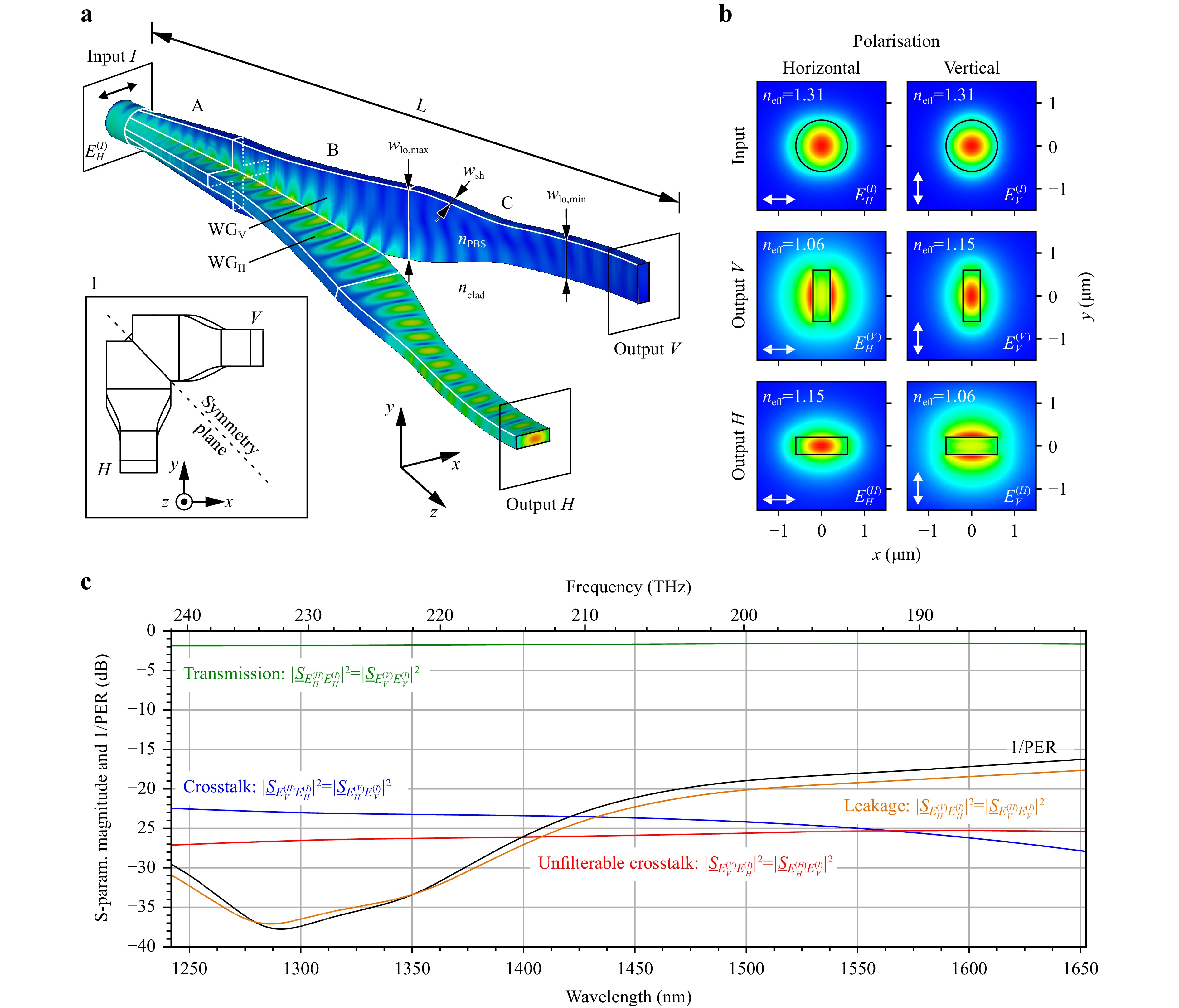
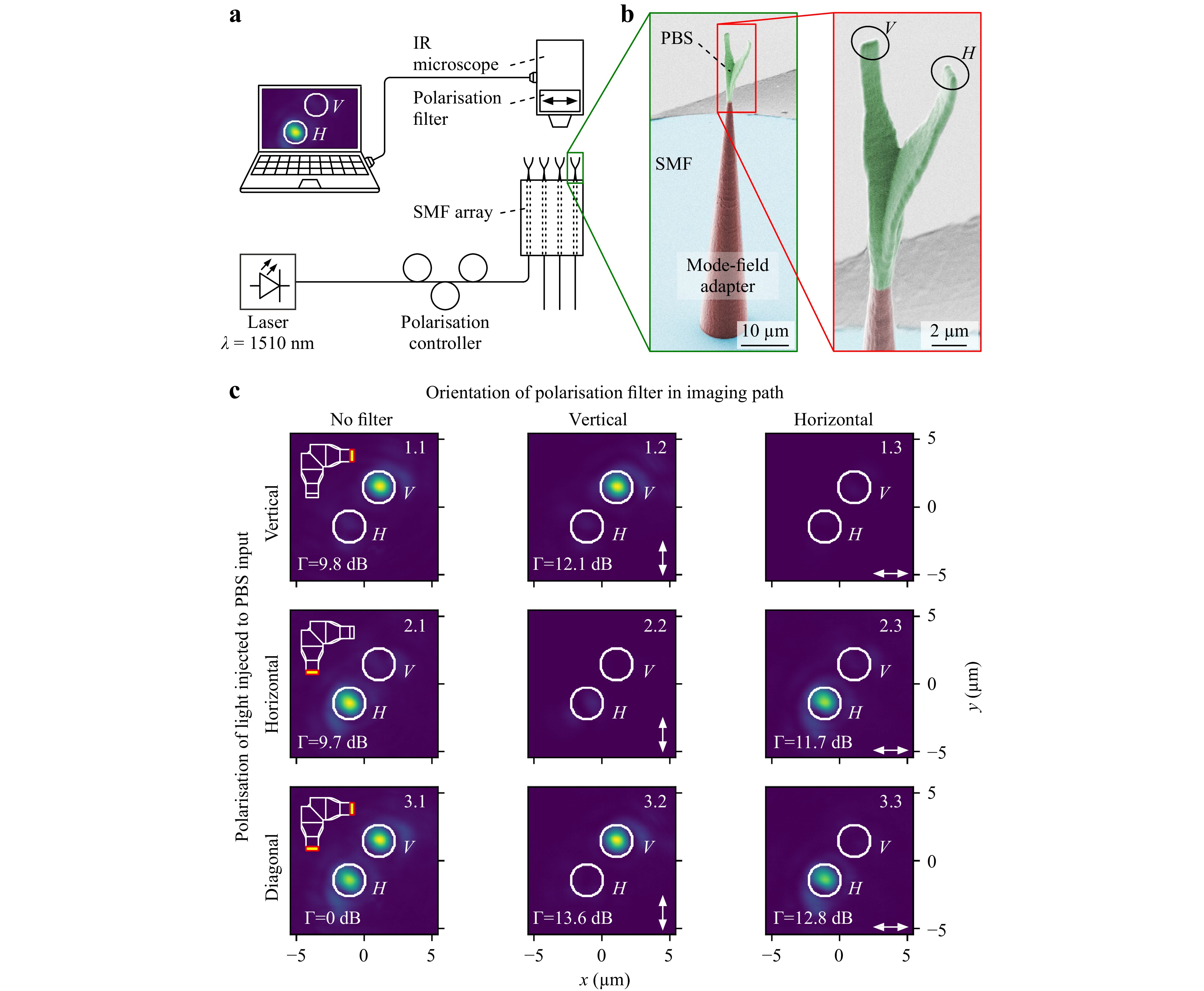
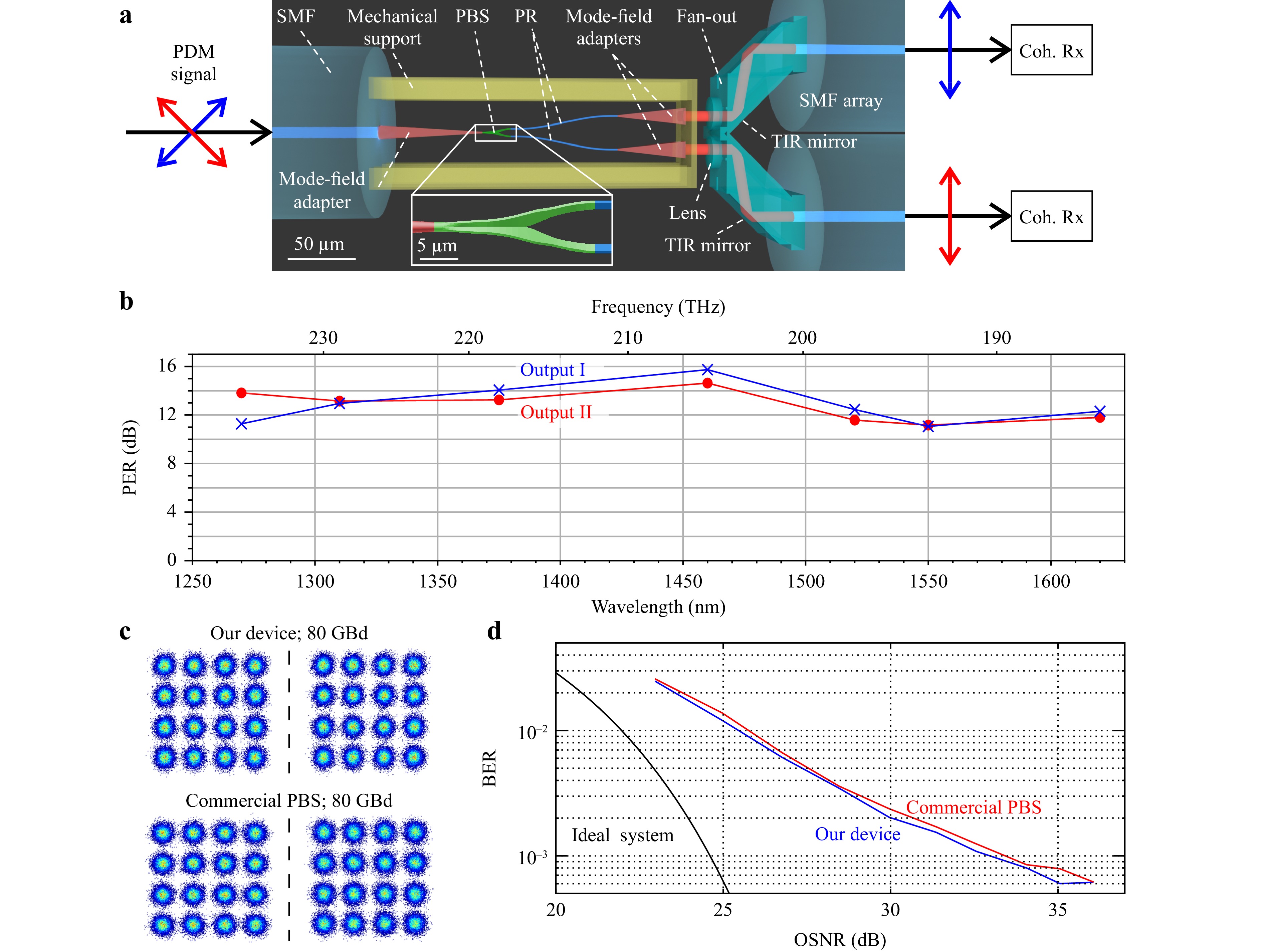
Multi-photon lithography has emerged as a powerful tool for photonic integration, allowing to complement planar photonic circuits by 3D-printed freeform structures such as waveguides or micro-optical elements. These structures can be fabricated with a high precision on the facets of optical devices and enable highly efficient package-level chip–chip connections in photonic assemblies. However, plain light transport and efficient coupling is far from exploiting the full geometrical design freedom offered by 3D laser lithography. Here, we extended the functionality of 3D-printed optical structures to manipulation of optical polarisation states. We demonstrate compact ultra-broadband polarisation beam splitters (PBSs) that can be combined with polarisation rotators and mode-field adapters into a monolithic 3D-printed structure, fabricated directly on the facets of optical devices. In a proof-of-concept experiment, we demonstrate measured polarisation extinction ratios beyond 11 dB over a bandwidth of 350 nm at near-infrared telecommunication wavelengths around 1550 nm. We demonstrate the viability of the device by receiving a 640 Gbit/s dual-polarisation data signal using 16-state quadrature amplitude modulation (16QAM), without any measurable optical-signal-to-noise-ratio penalty compared to a commercial PBS.
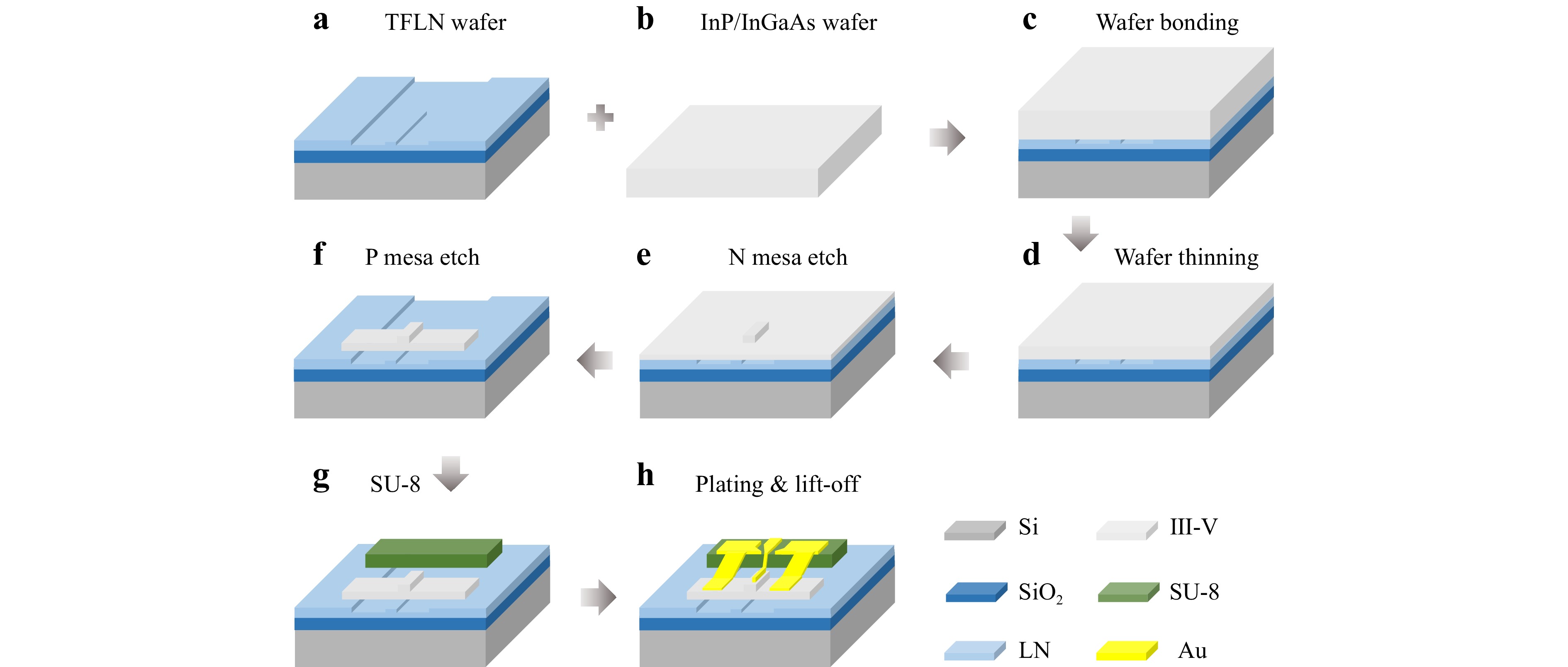
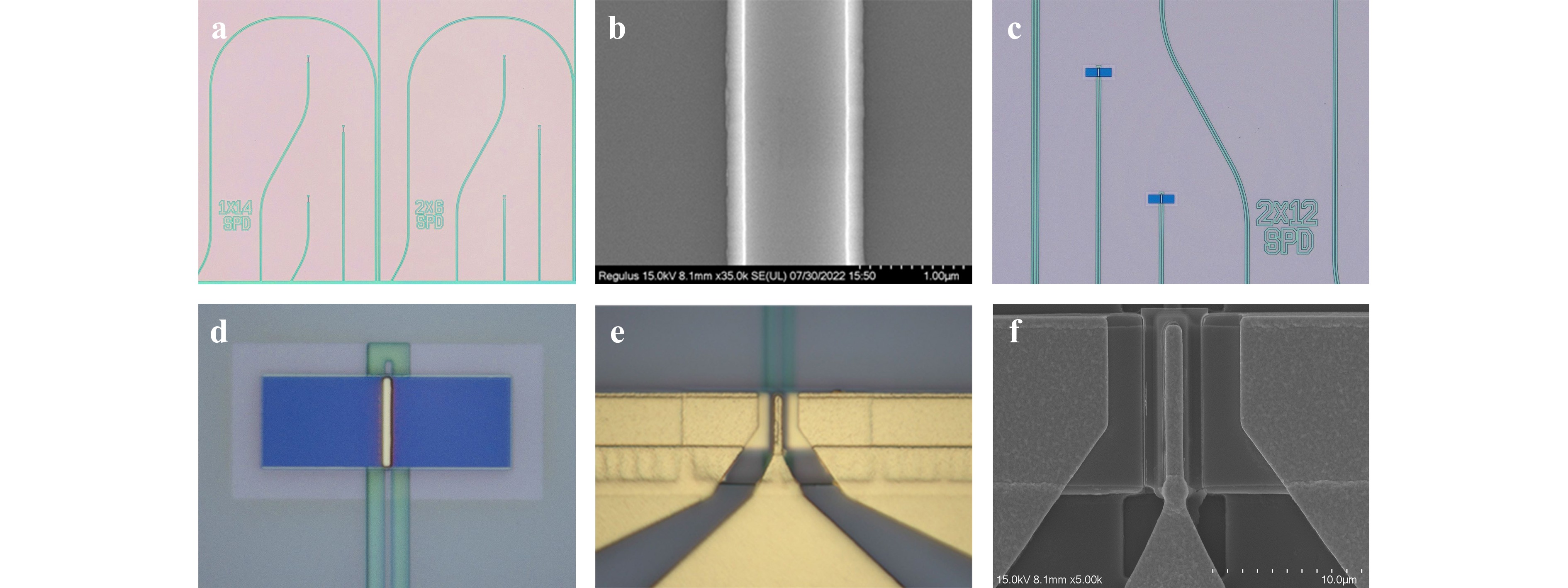
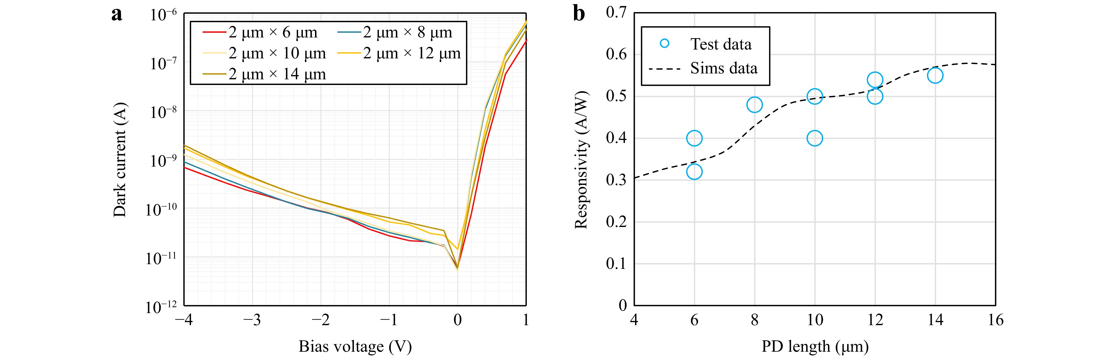
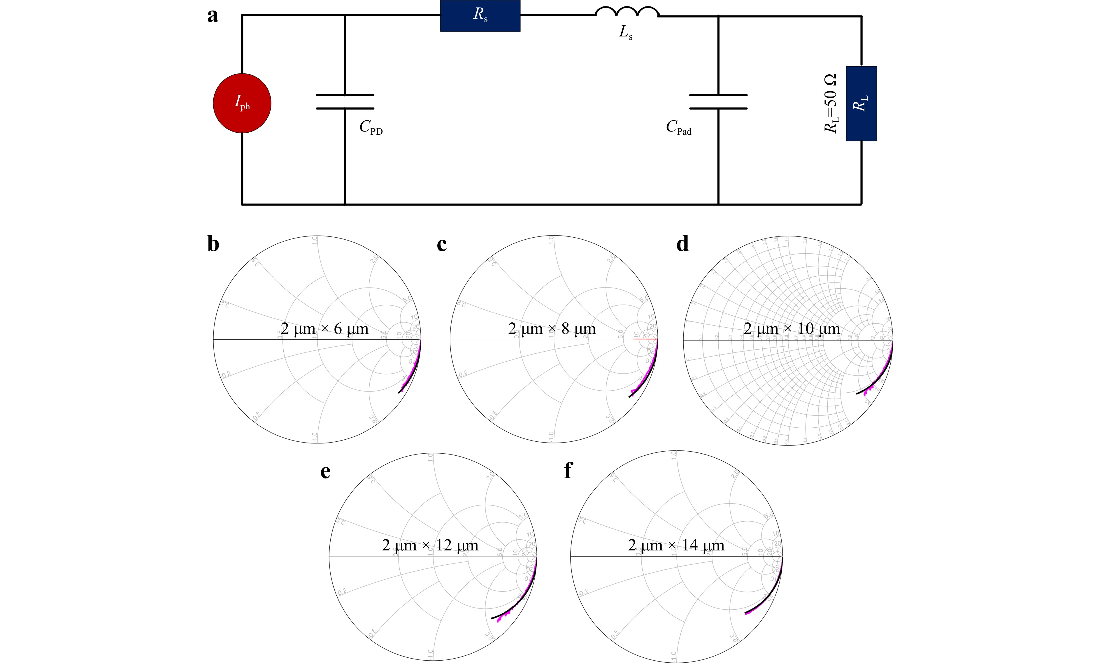
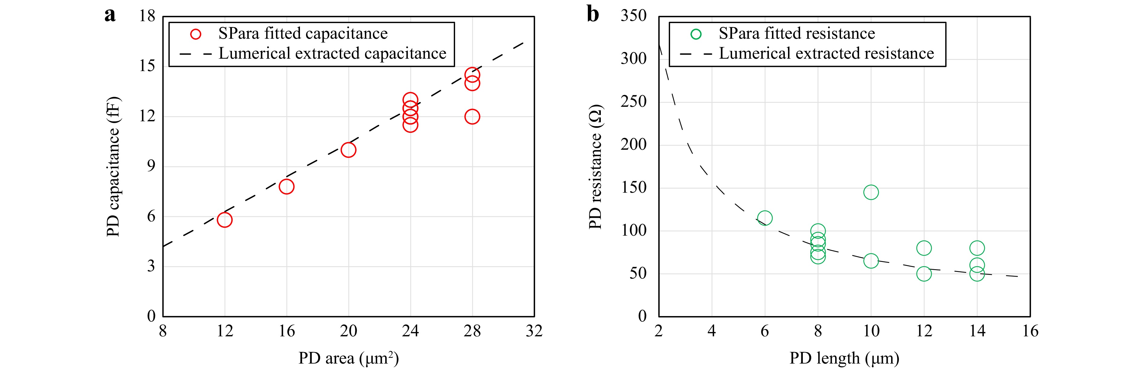
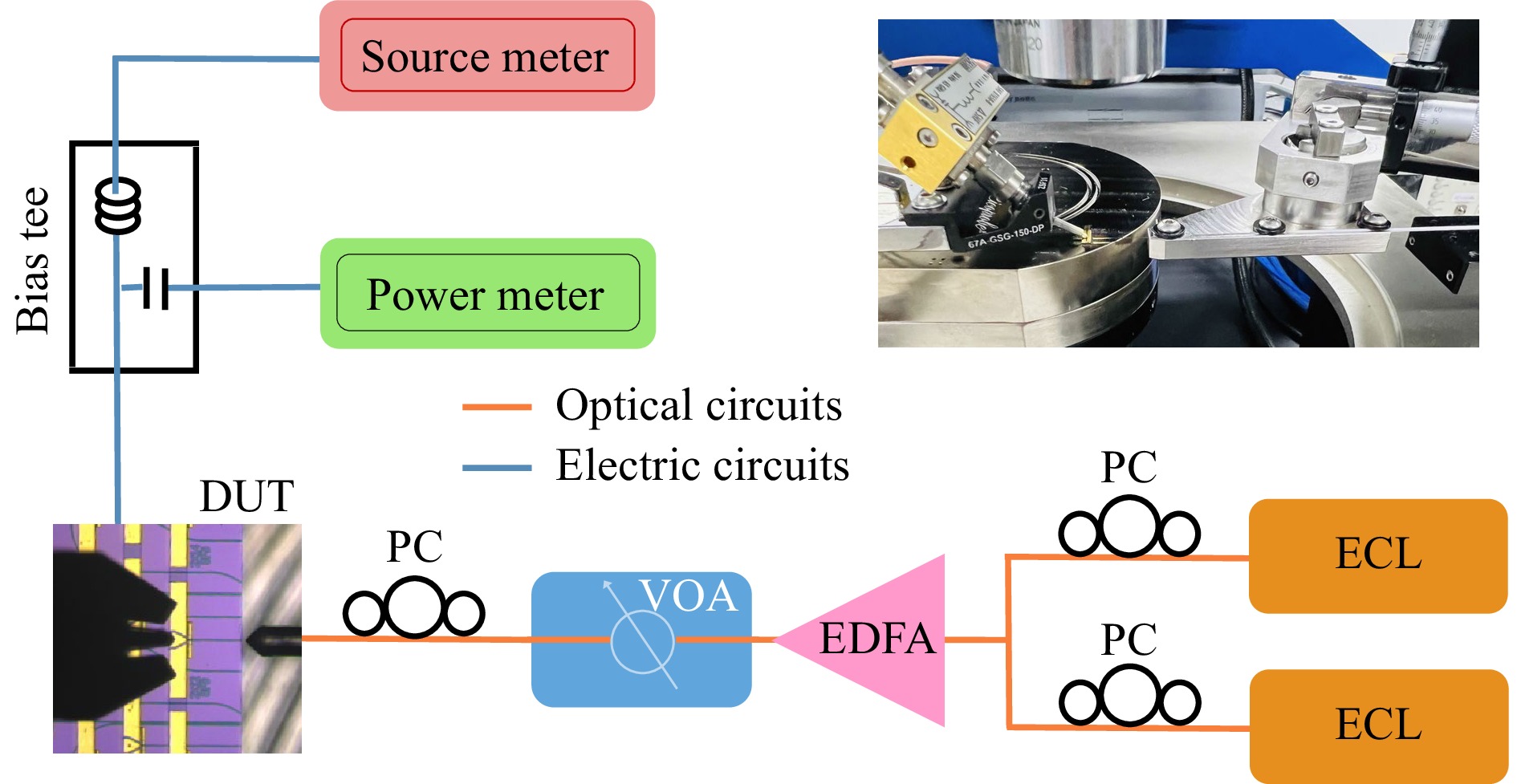
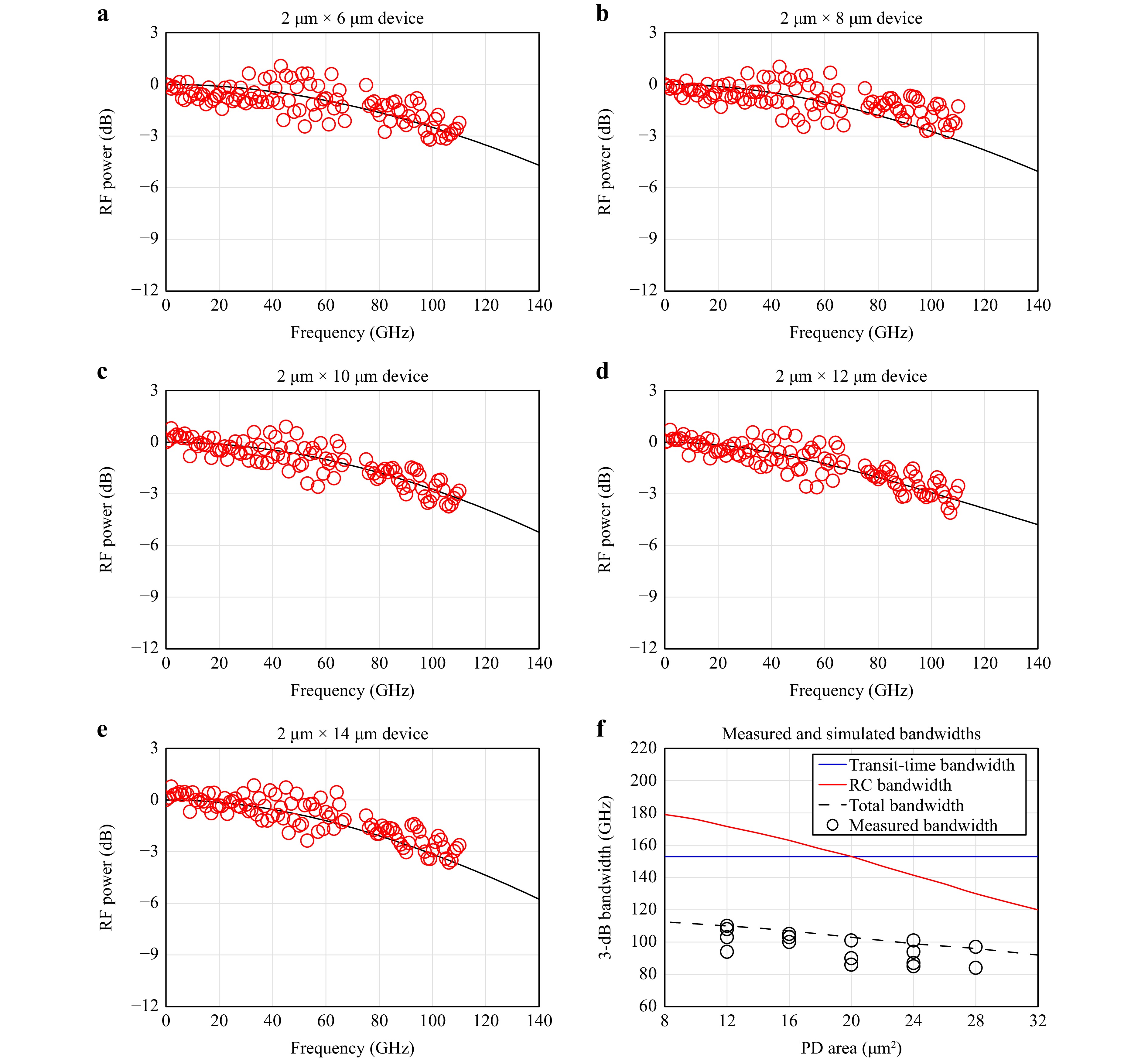
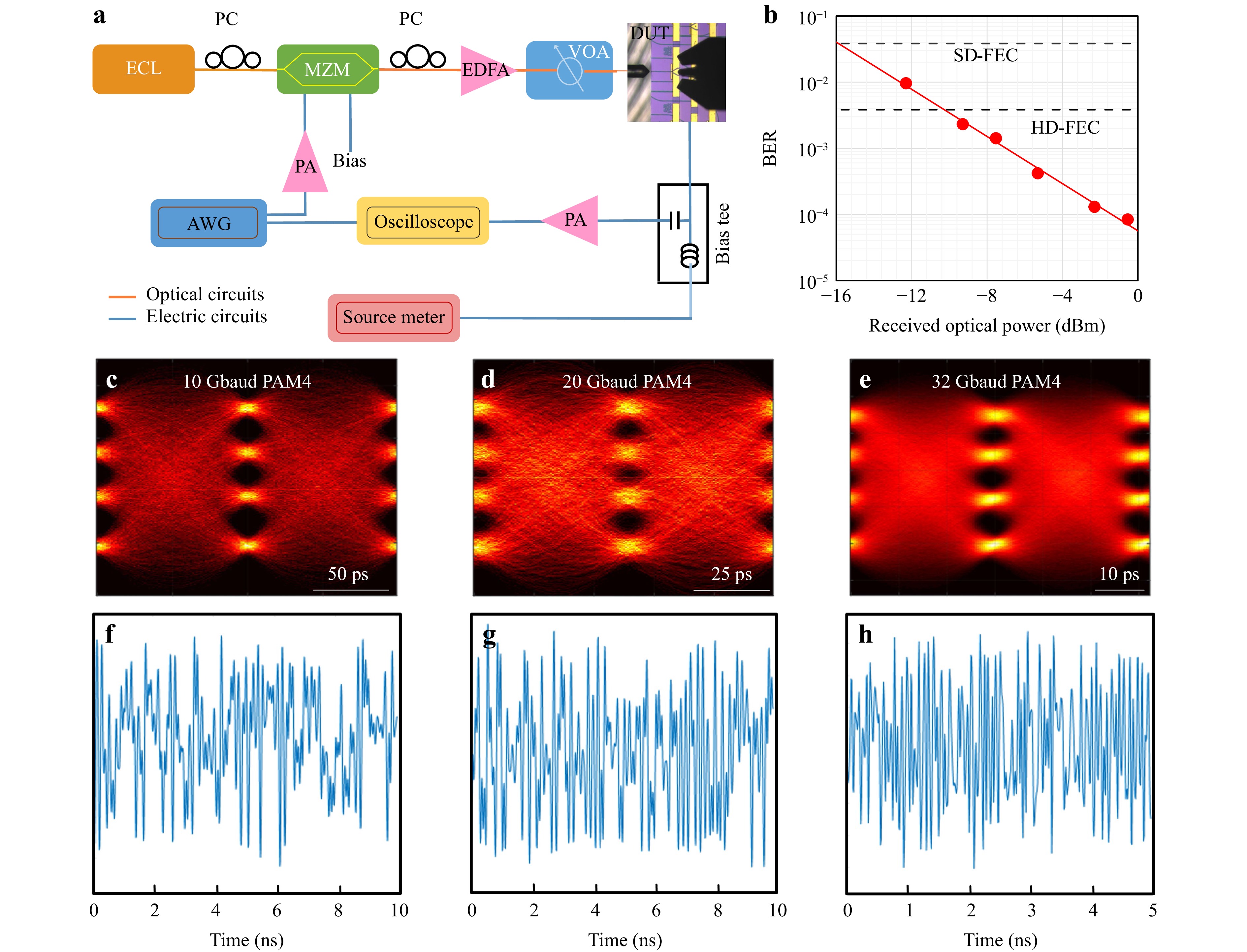
With the advantages of large electro-optical coefficient, wide transparency window, and strong optical confinement, thin-film lithium niobate (TFLN) technique has enabled the development of various high-performance optoelectronics devices, ranging from the ultra-wideband electro-optic modulators to the high-efficient quantum sources. However, the TFLN platform does not natively promise lasers and photodiodes. This study presents an InP/InGaAs modified uni-traveling carrier (MUTC) photodiodes heterogeneously integrated on the TFLN platform with a record-high 3-dB bandwidth of 110 GHz and a responsivity of 0.4 A/W at a 1,550-nm wavelength. It is implemented in a wafer-level TFLN-InP heterogeneous integration platform and is suitable for the large-scale, multi-function, and high-performance TFLN photonic integrated circuits.
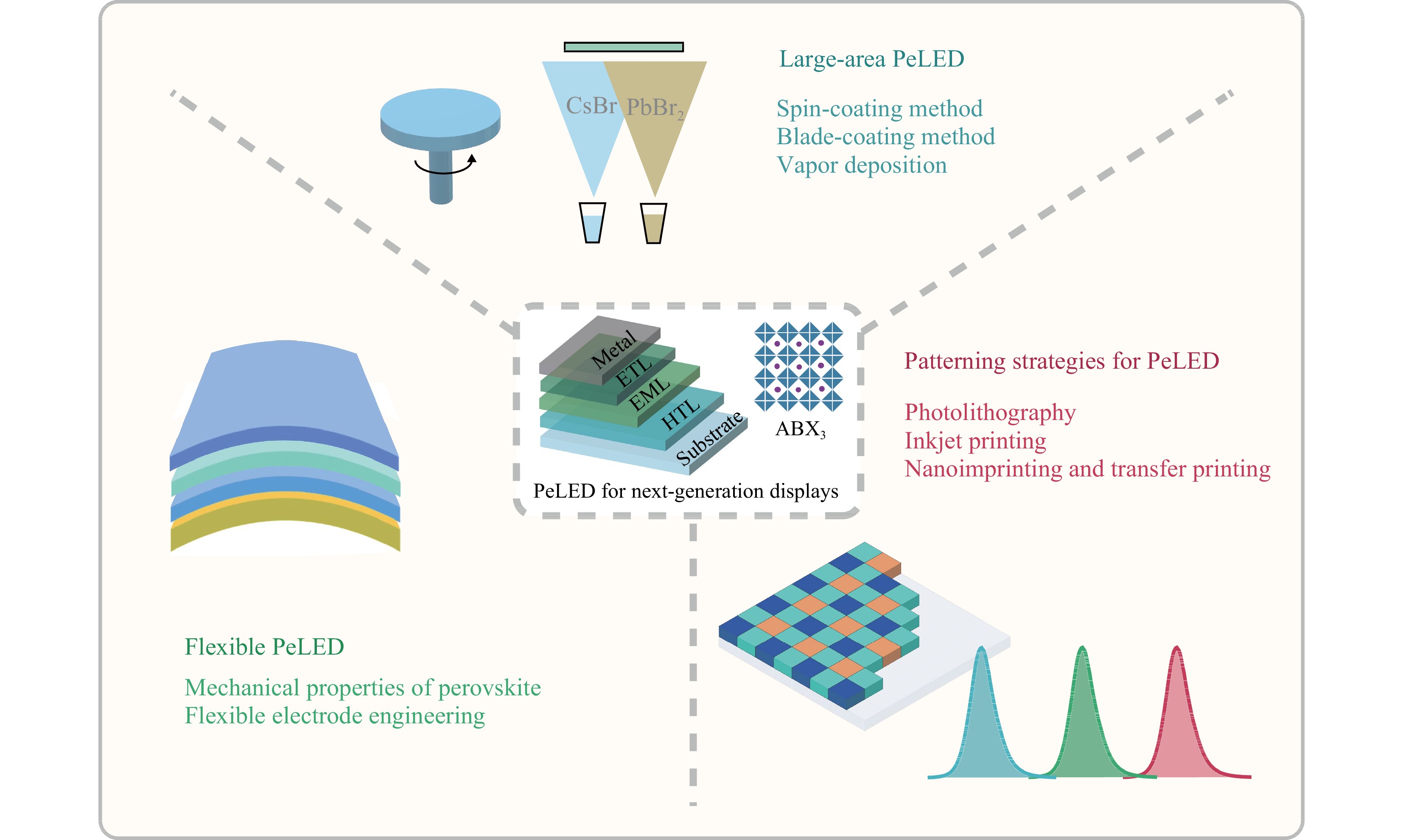
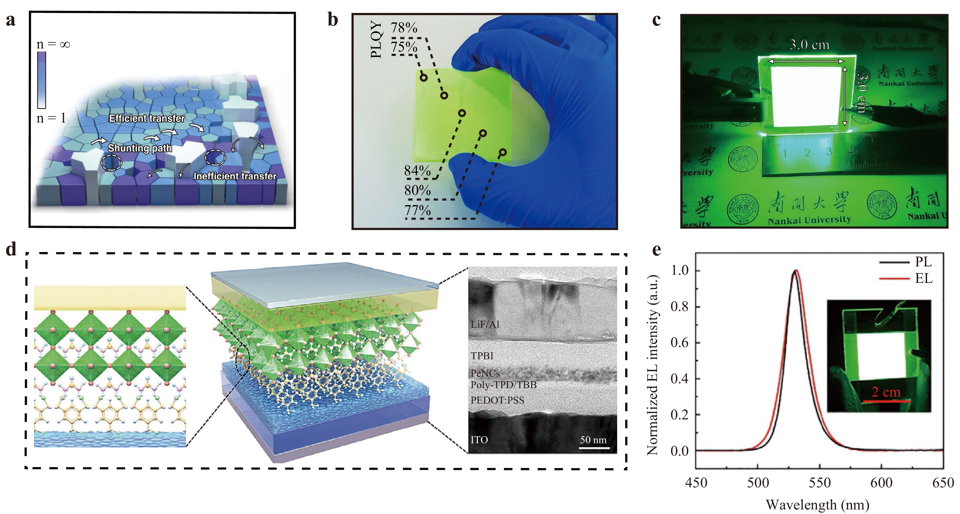
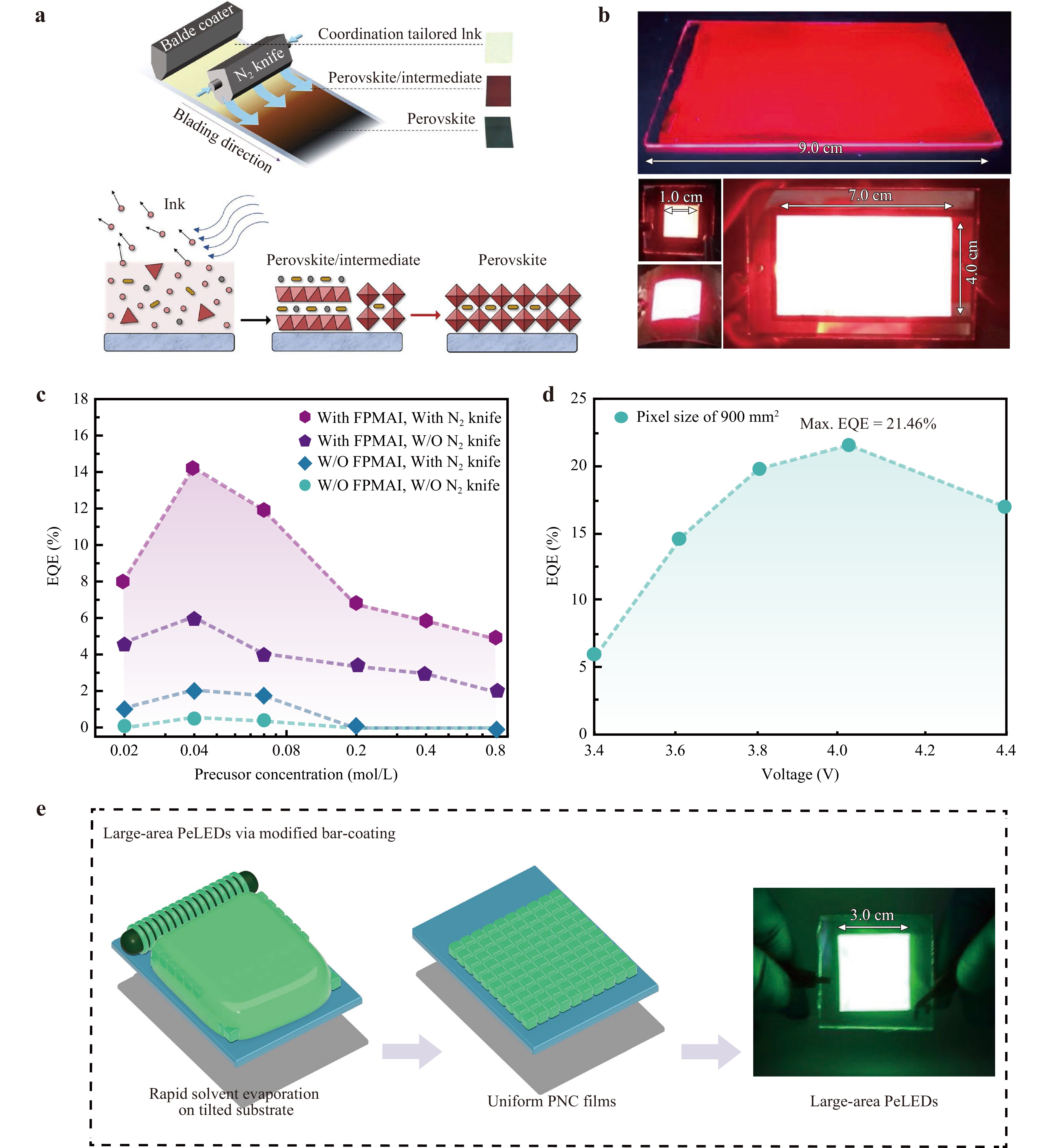
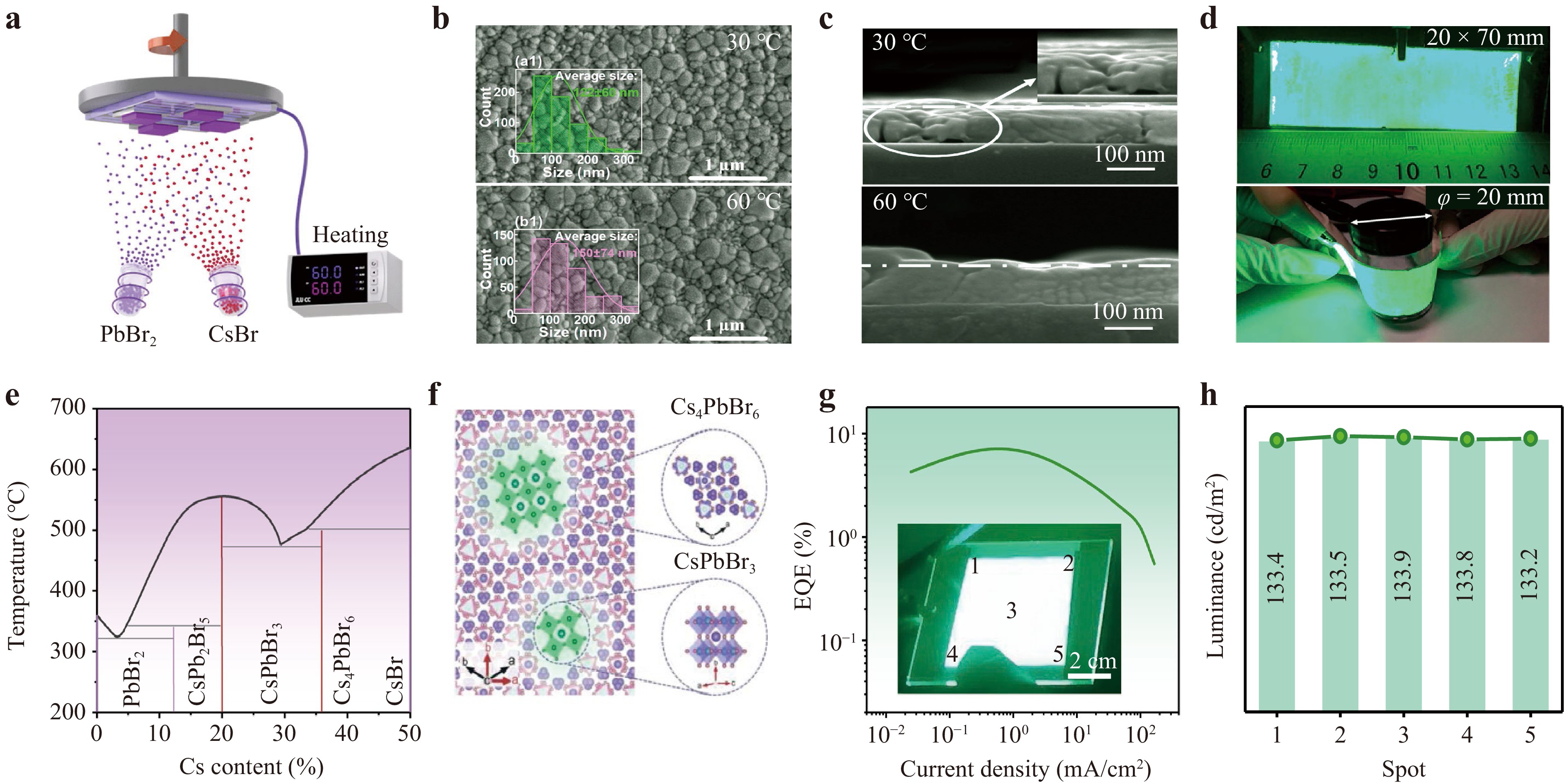
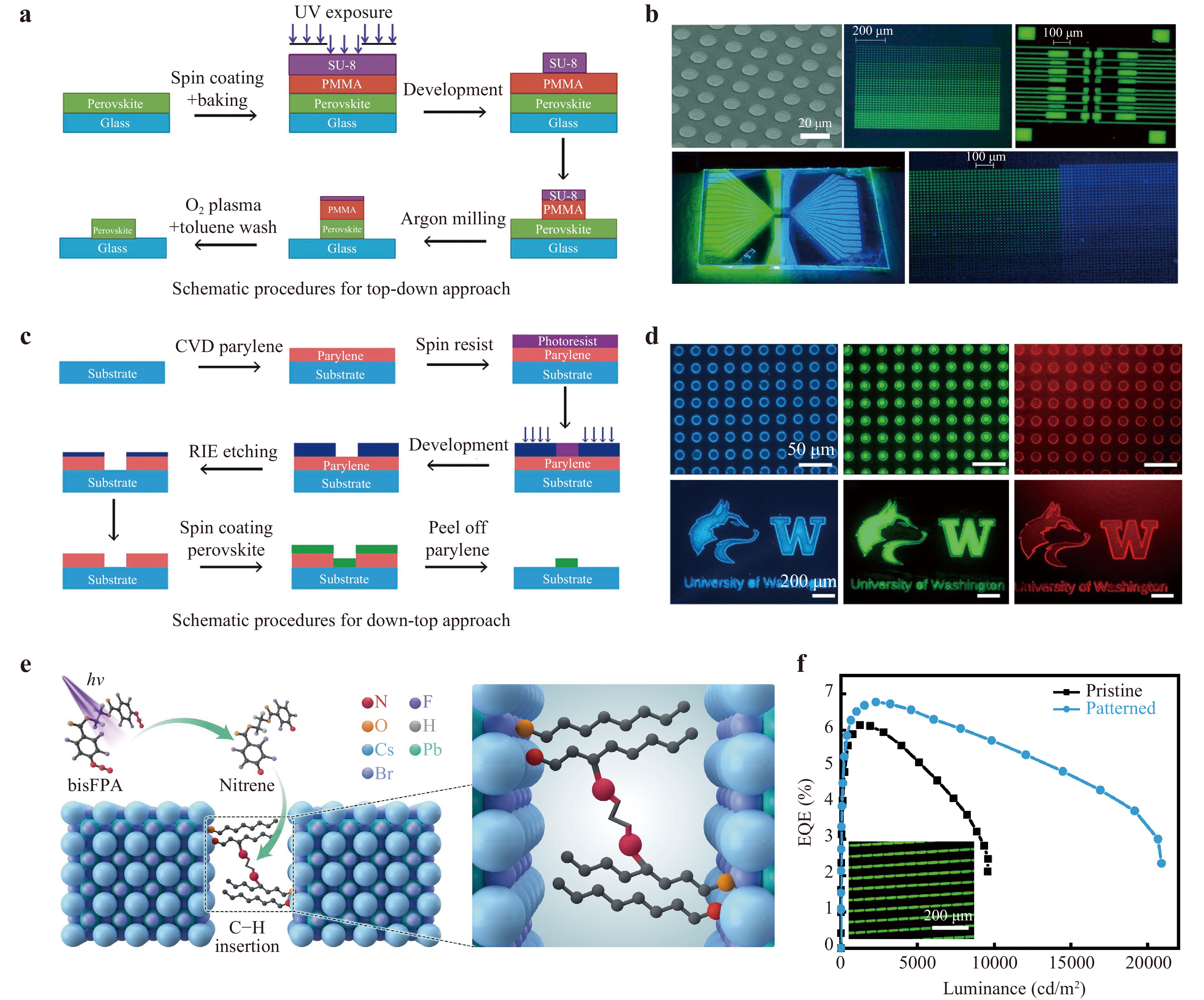
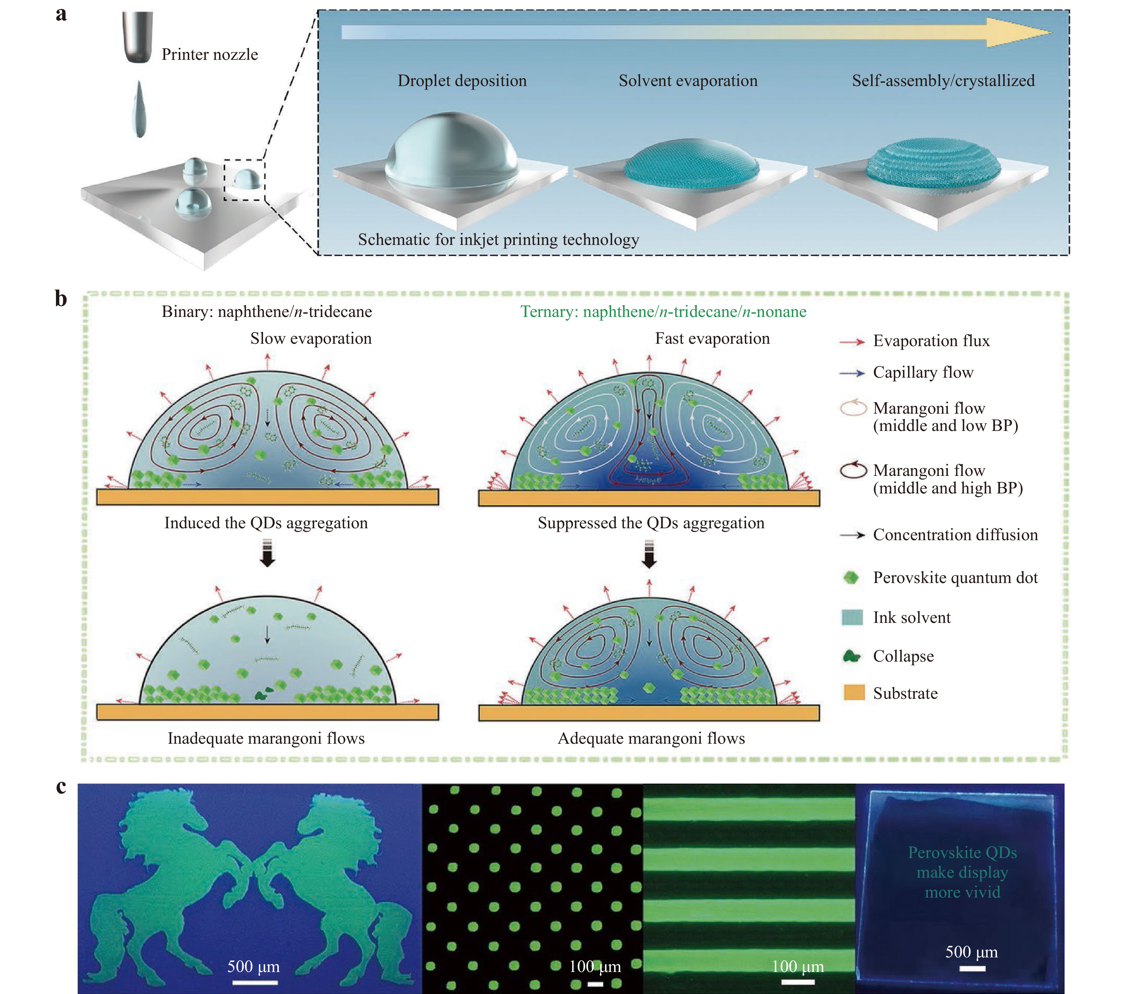
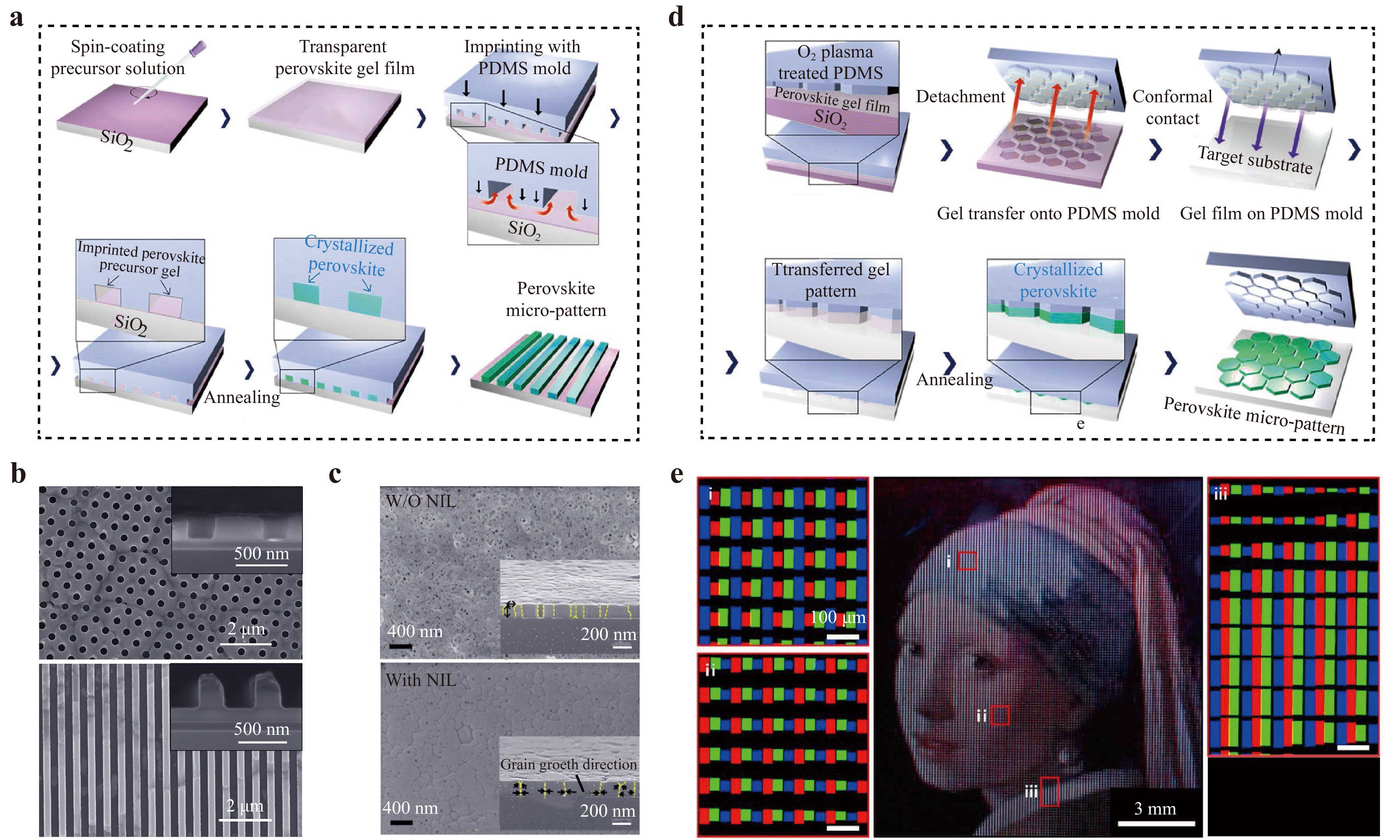
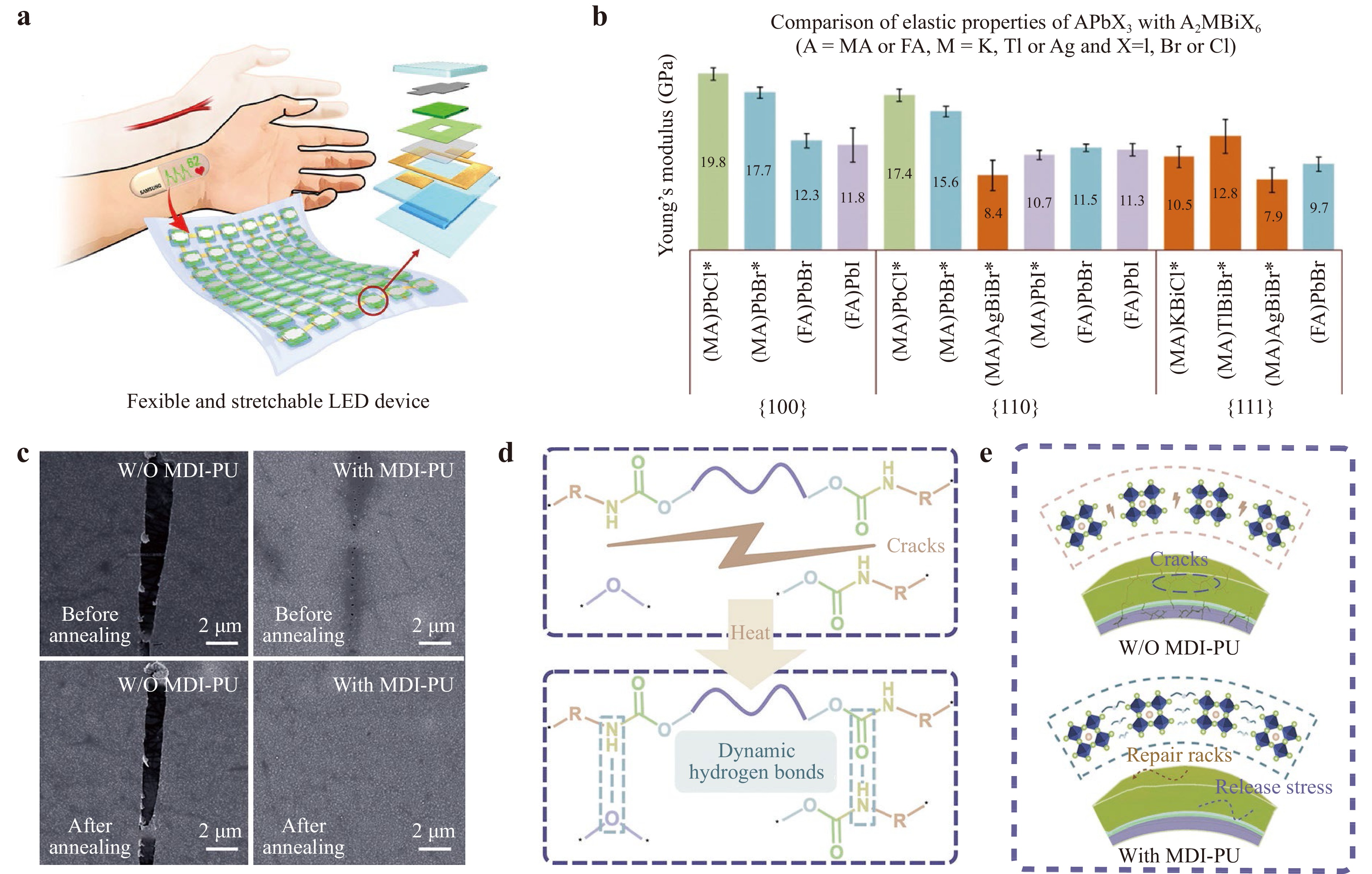
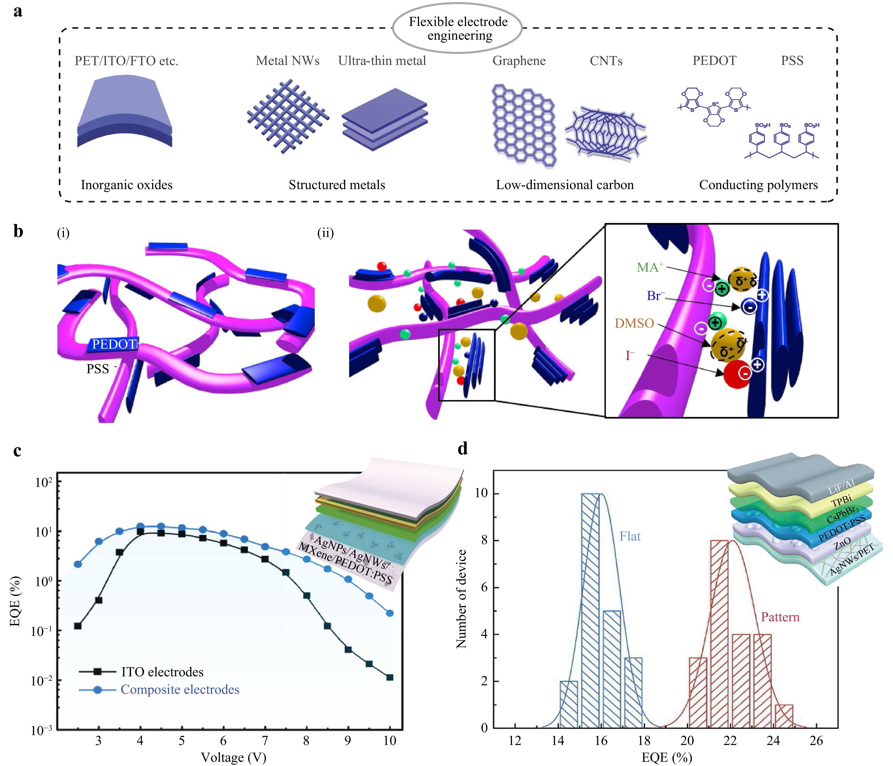
Metal-halide perovskite light-emitting diodes (PeLEDs) possess wide colour gamut, high luminescence efficiency, and low-cost synthesis, making them a promising photonic source for next-generation display applications. Since the first room-temperature emission PeLED was demonstrated in 2014, their performance has improved rapidly within a few years, leading to considerable attention from academia and industry. In this review, we discuss the primary technical bottlenecks of PeLEDs for commercial display applications, including large-area PeLED preparation, patterning strategies, and flexible PeLED devices. We review the technical approaches for achieving these targets and highlight the current challenges while providing an outlook for these perovskite materials and PeLED devices to meet the requirements of the next-generation high-colour-purity full-colour display market.
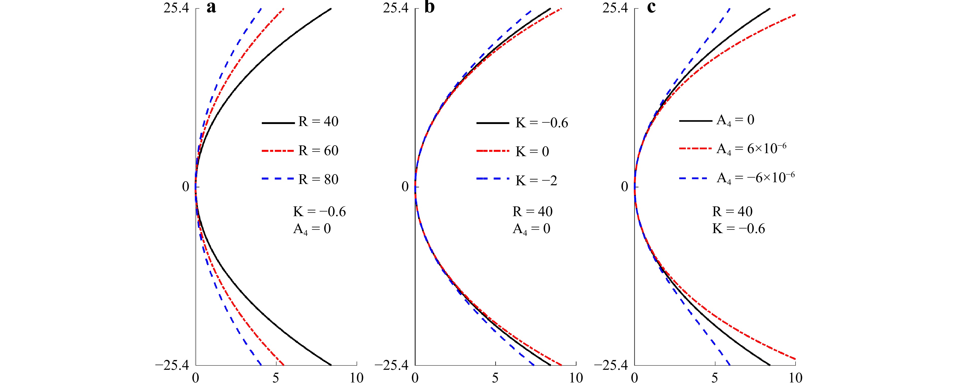
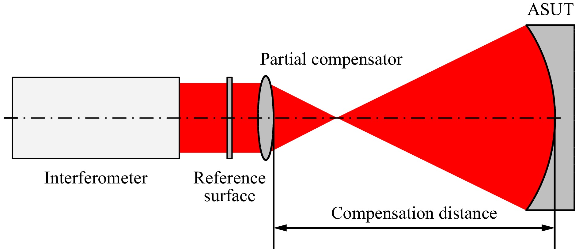
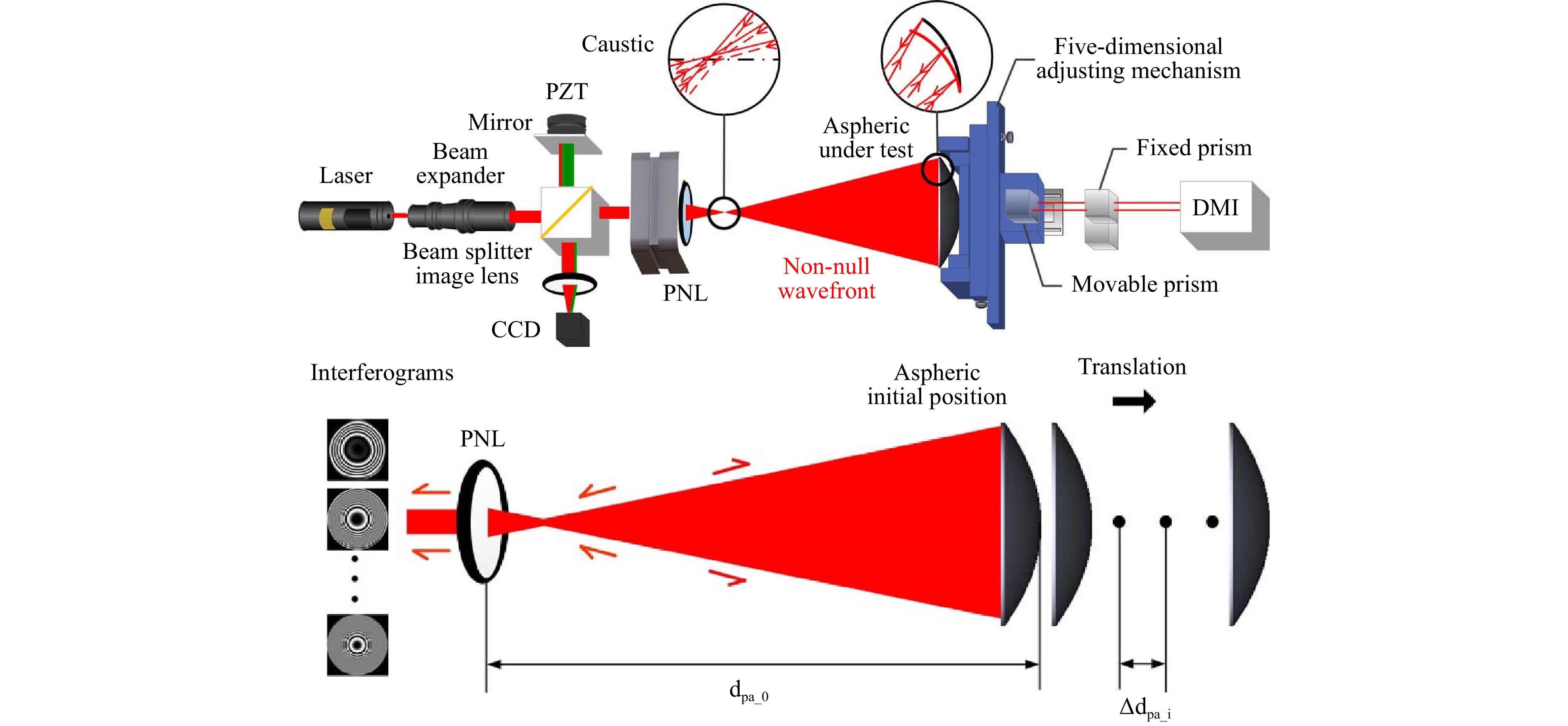
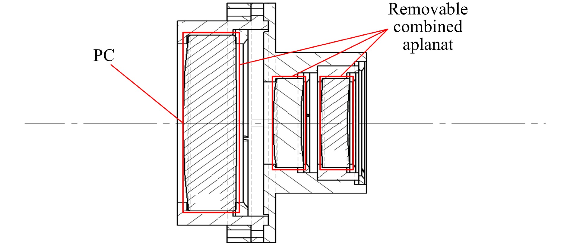
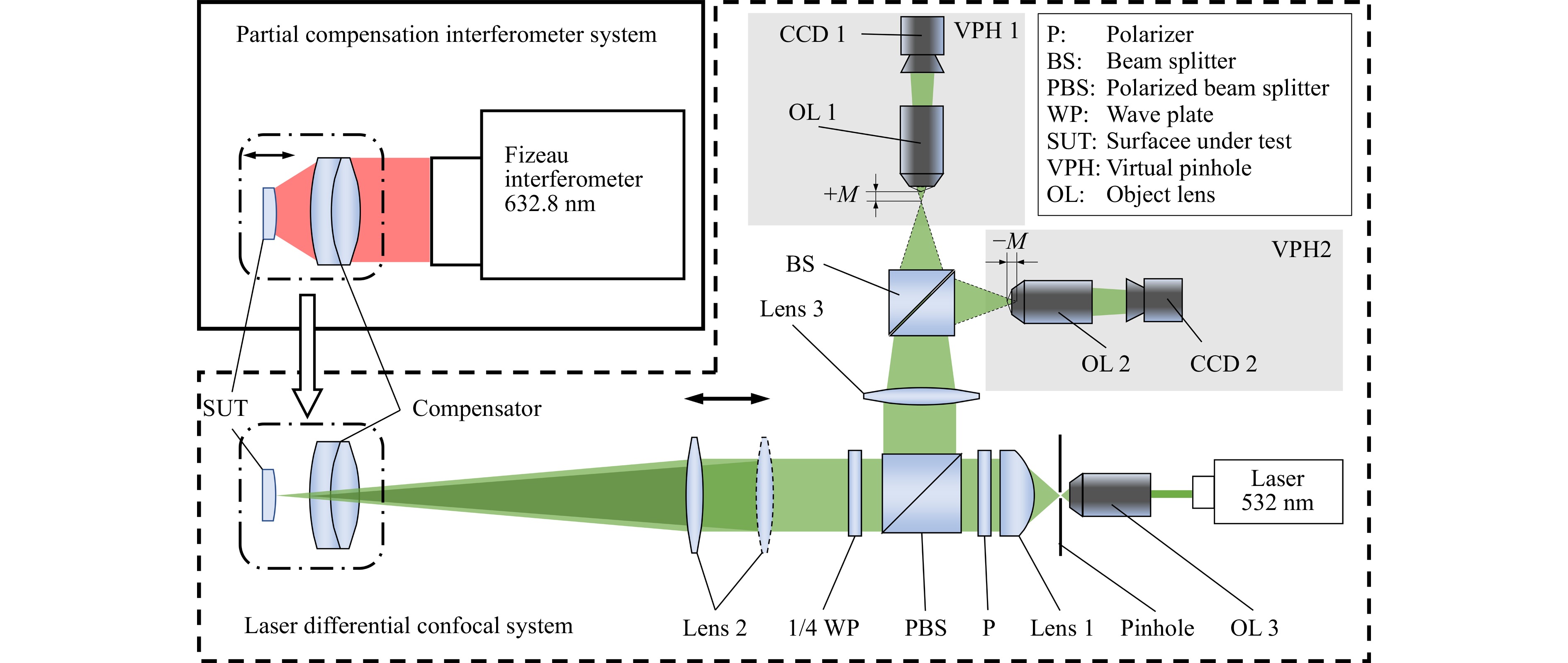
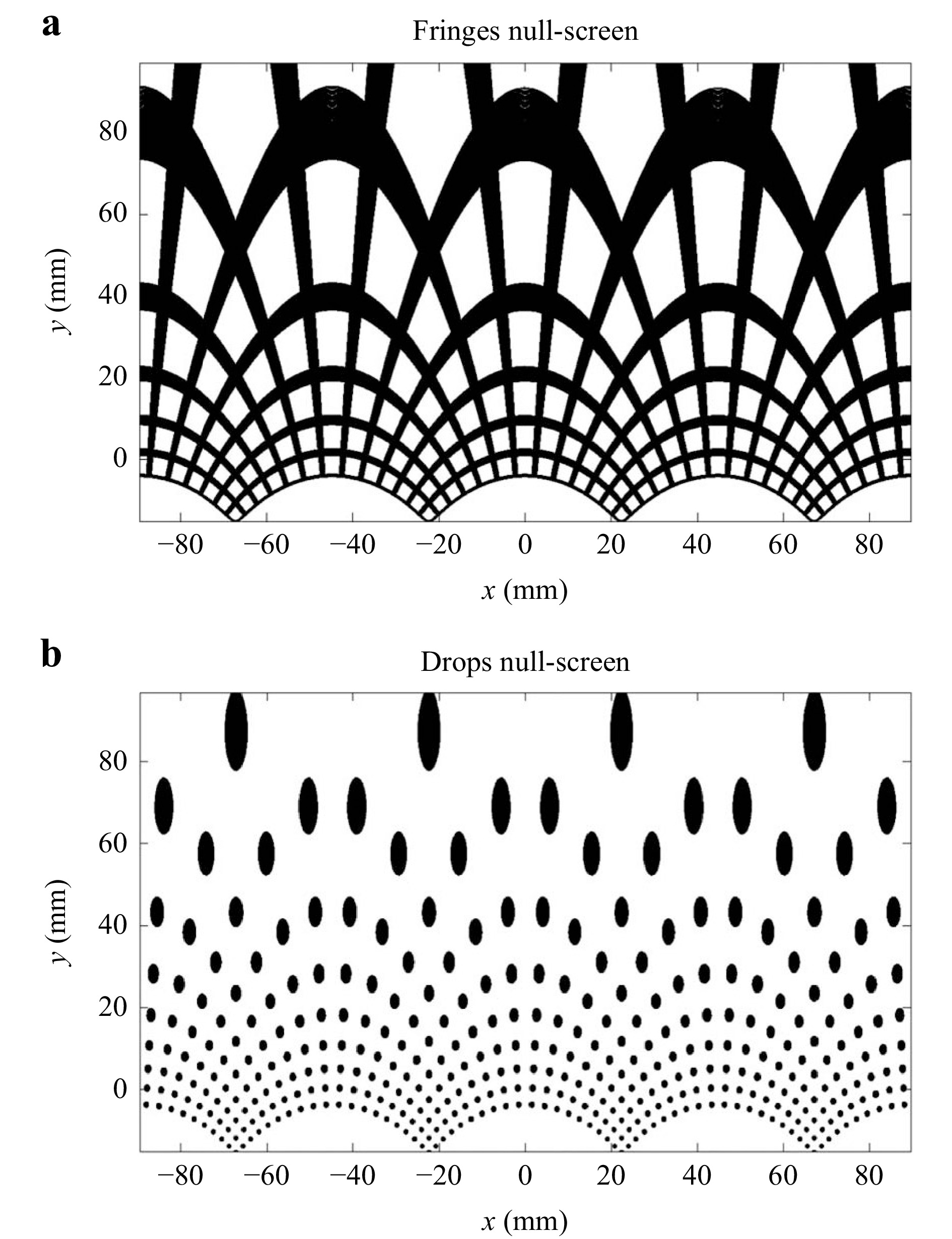
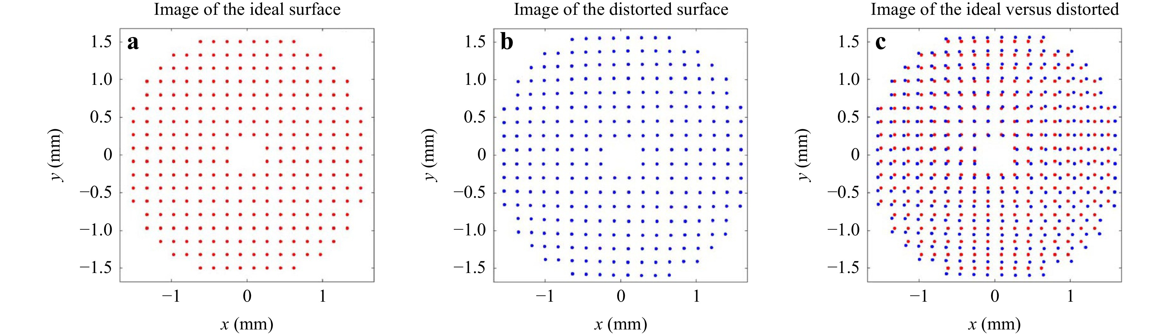
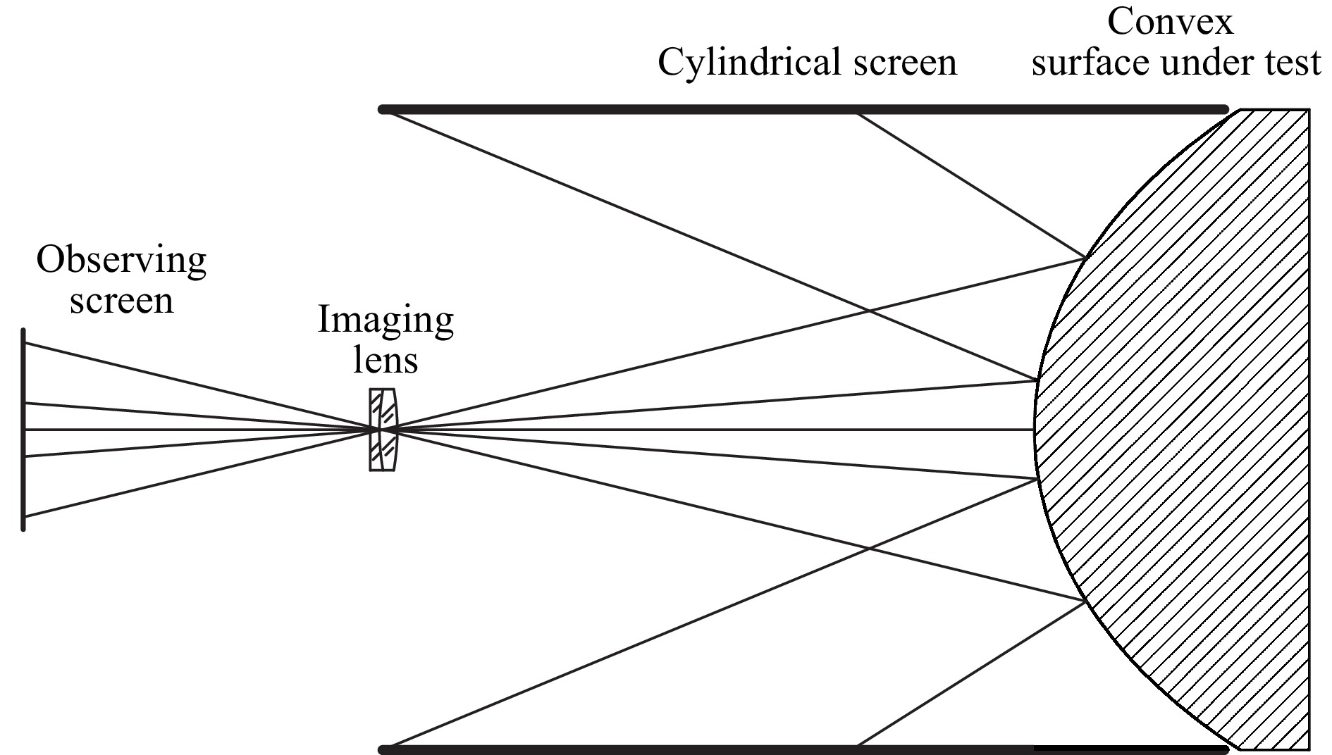
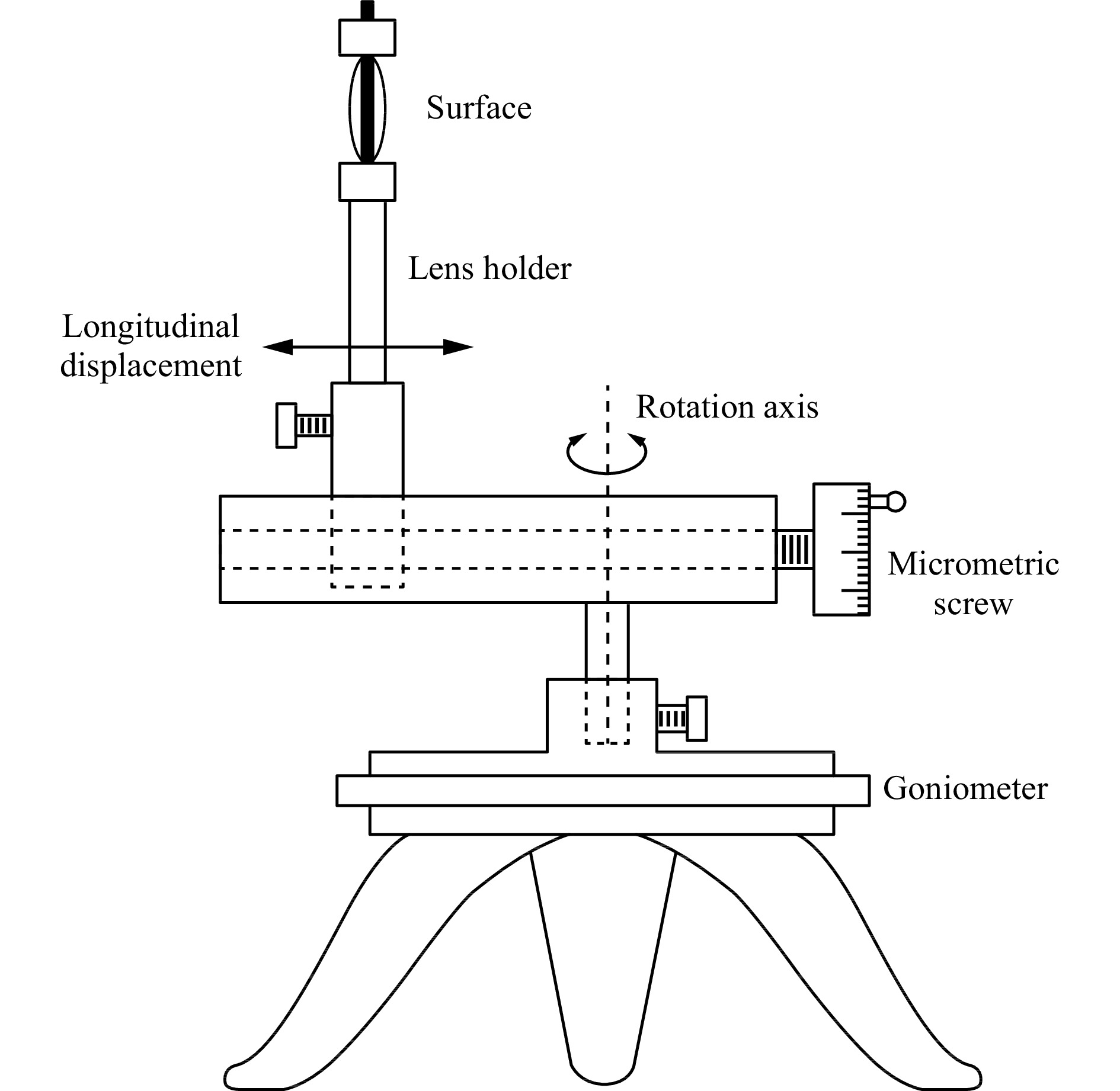
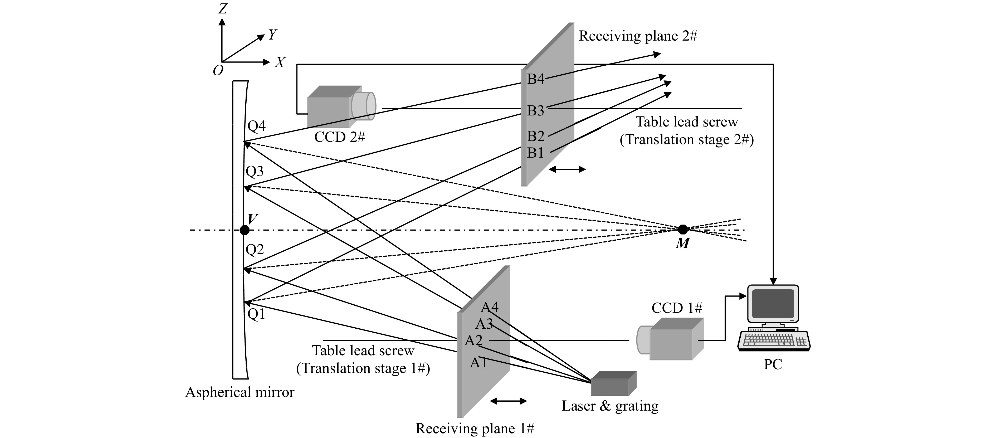
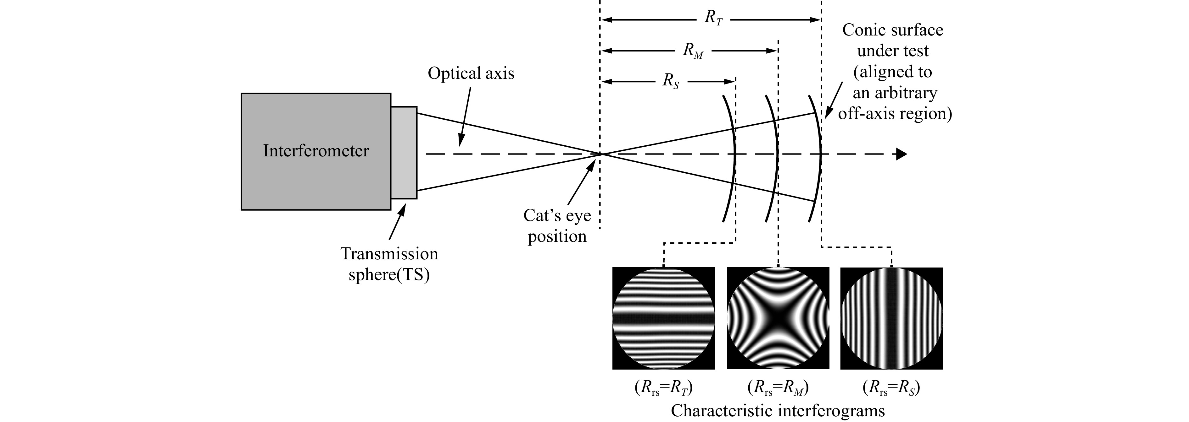
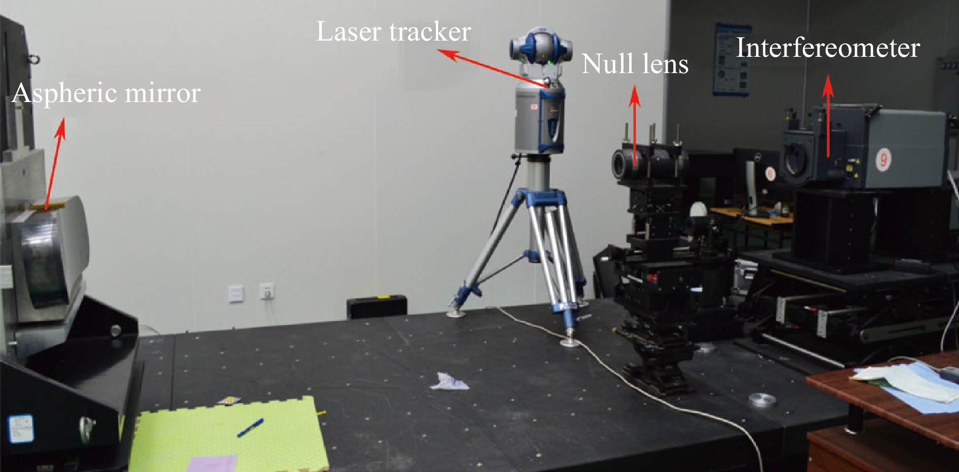
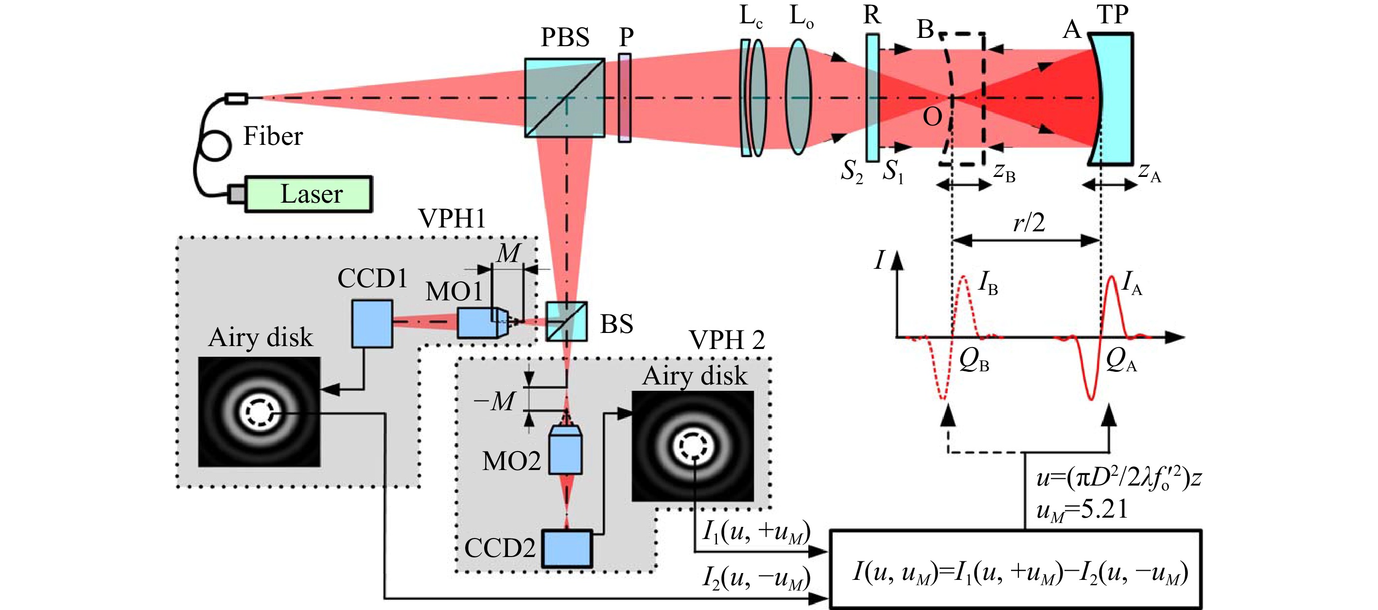
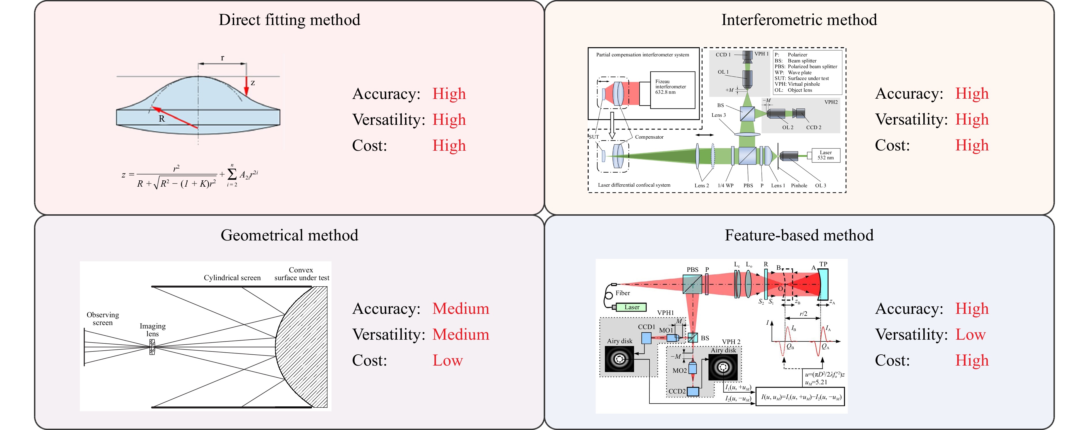
Aspheric surfaces are widely used in advanced optical instruments. Measuring the aspheric surface parameters (ASPs) with high accuracy is vital for manufacturing and aligning optical aspheric surfaces. This paper provides a review of various techniques for measuring ASPs and discusses the advantages/disadvantages of these approaches. The aim of this review is to contribute to advancements in the fabrication and testing of aspheric optical elements and their practical applications in diverse fields.

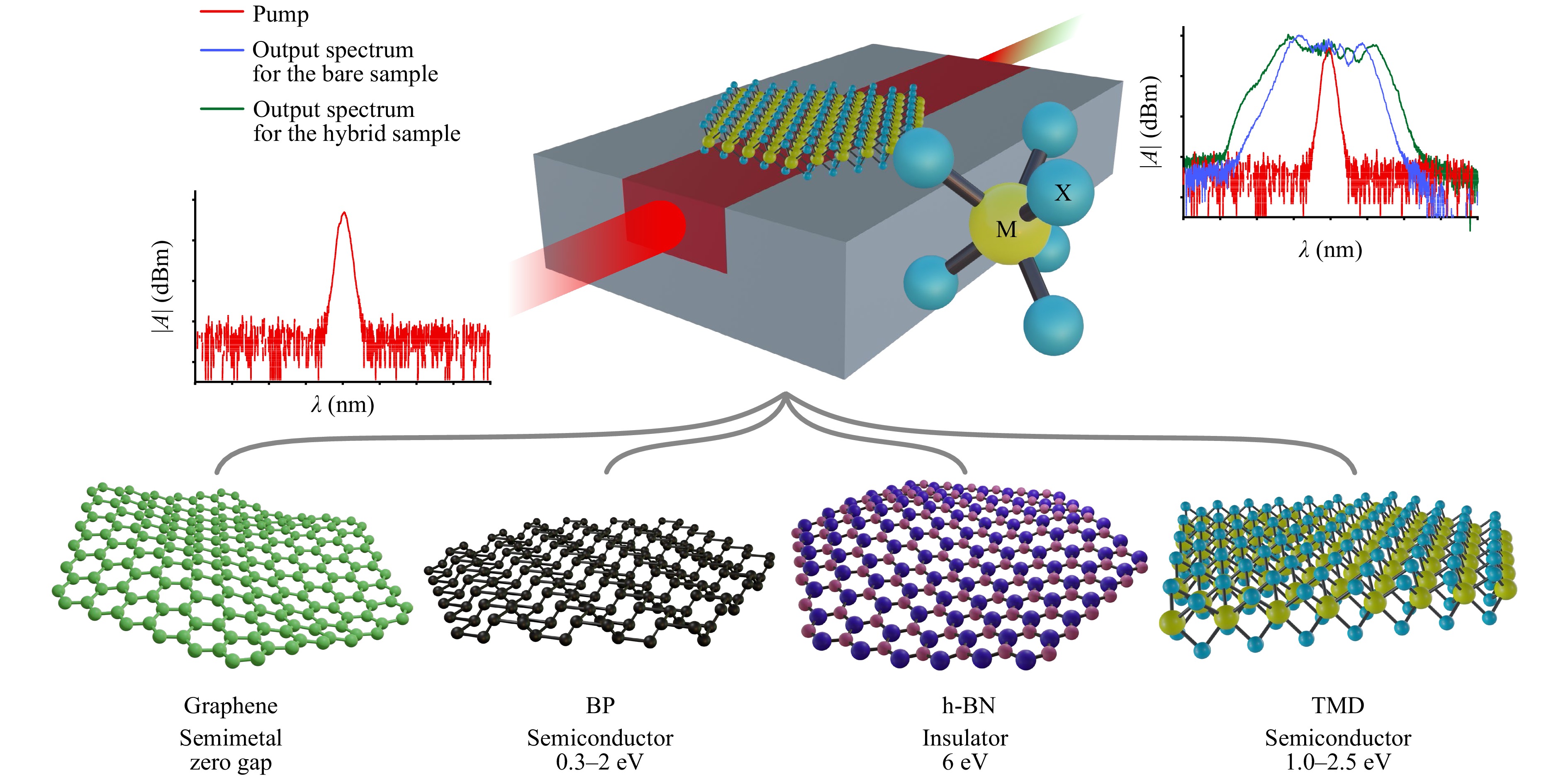
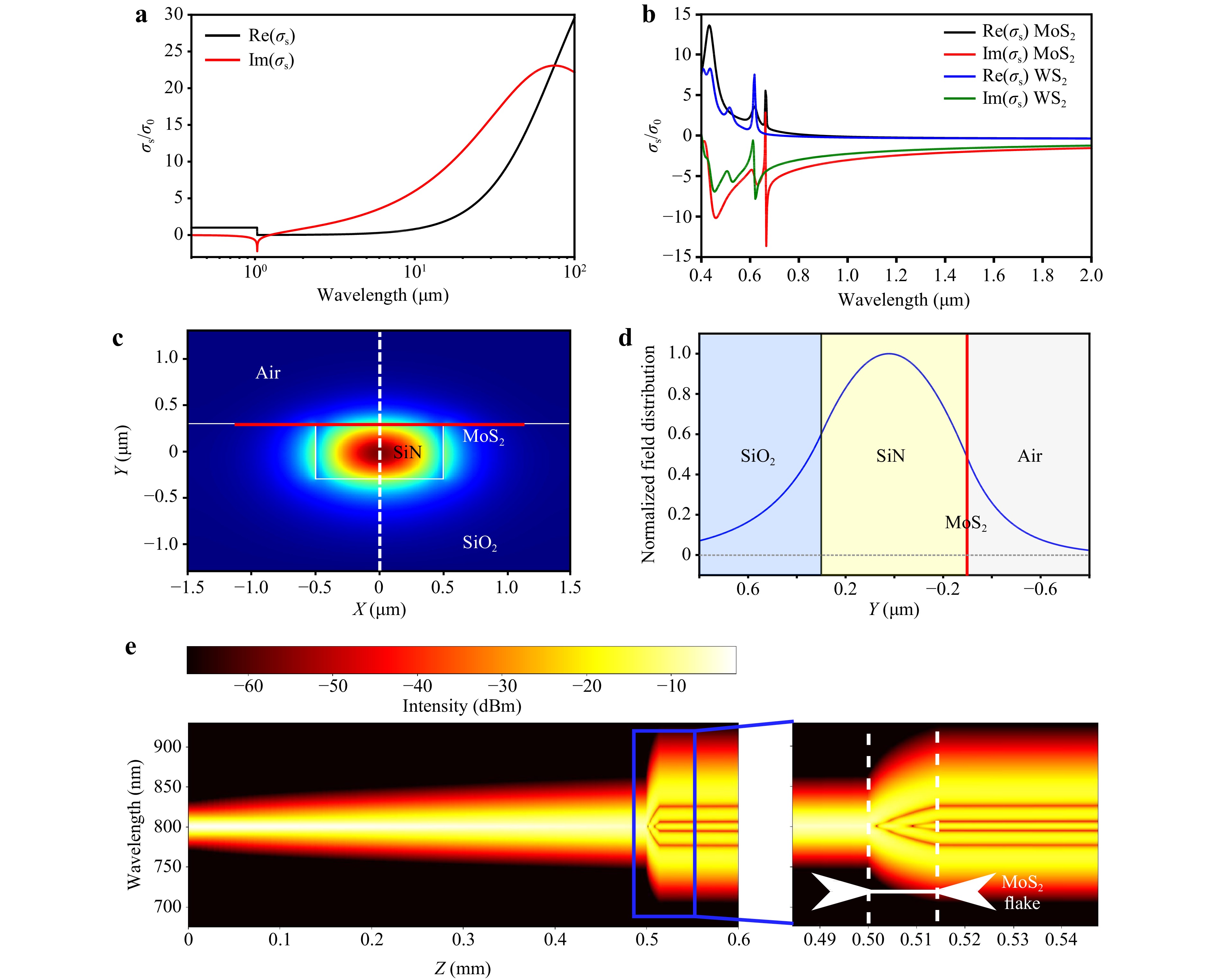
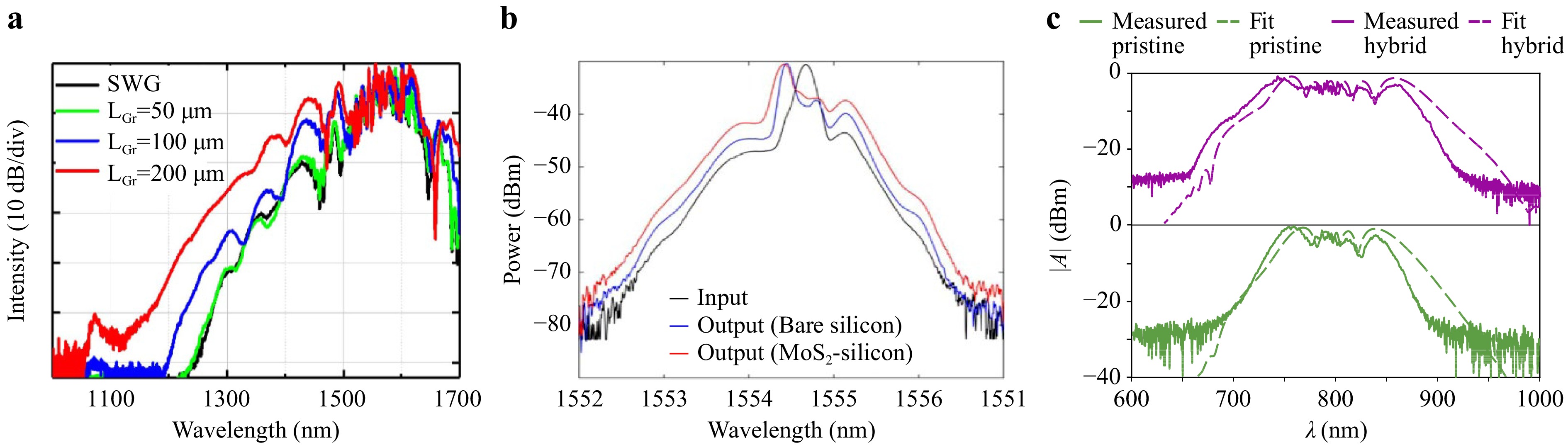
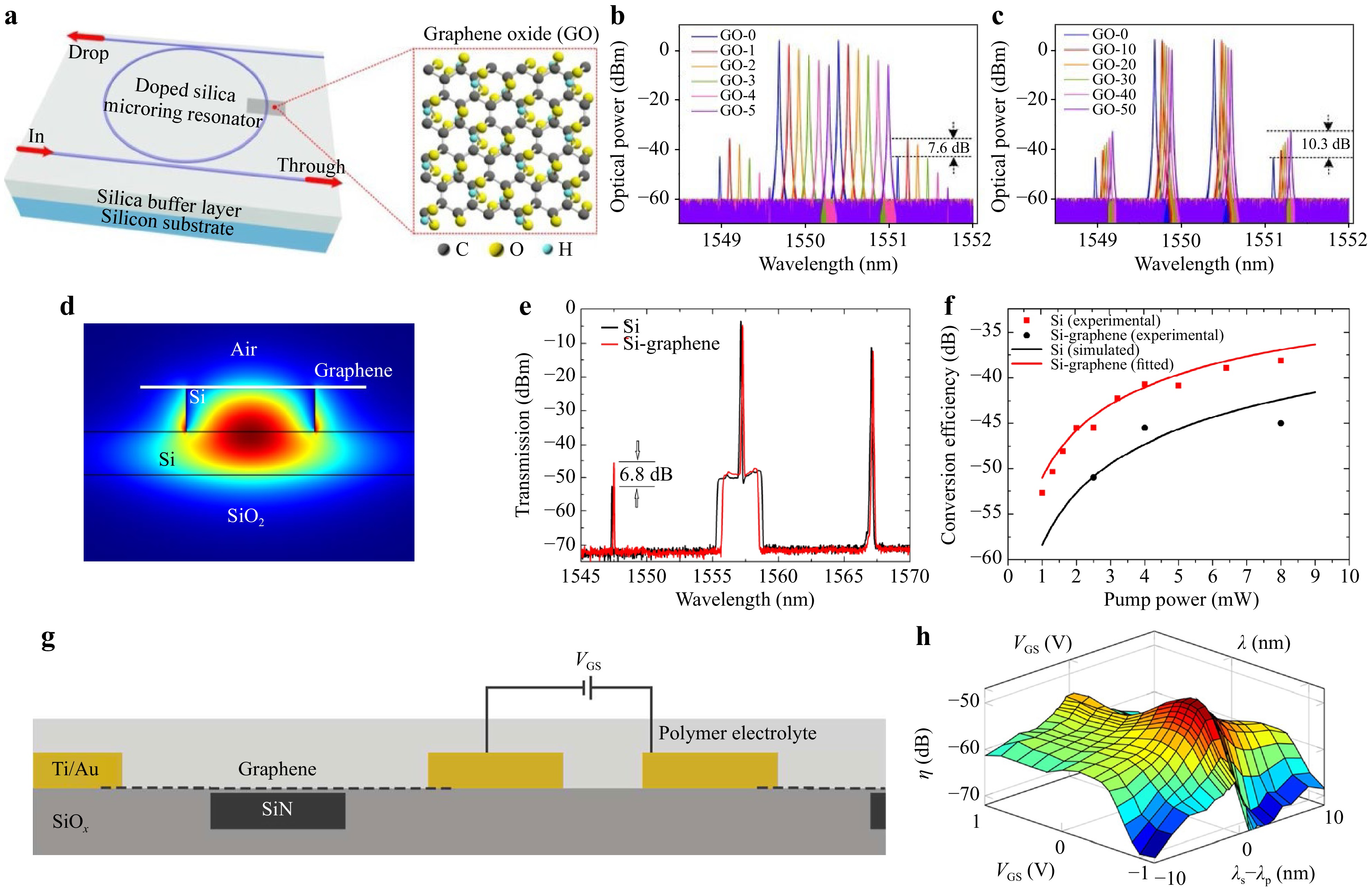
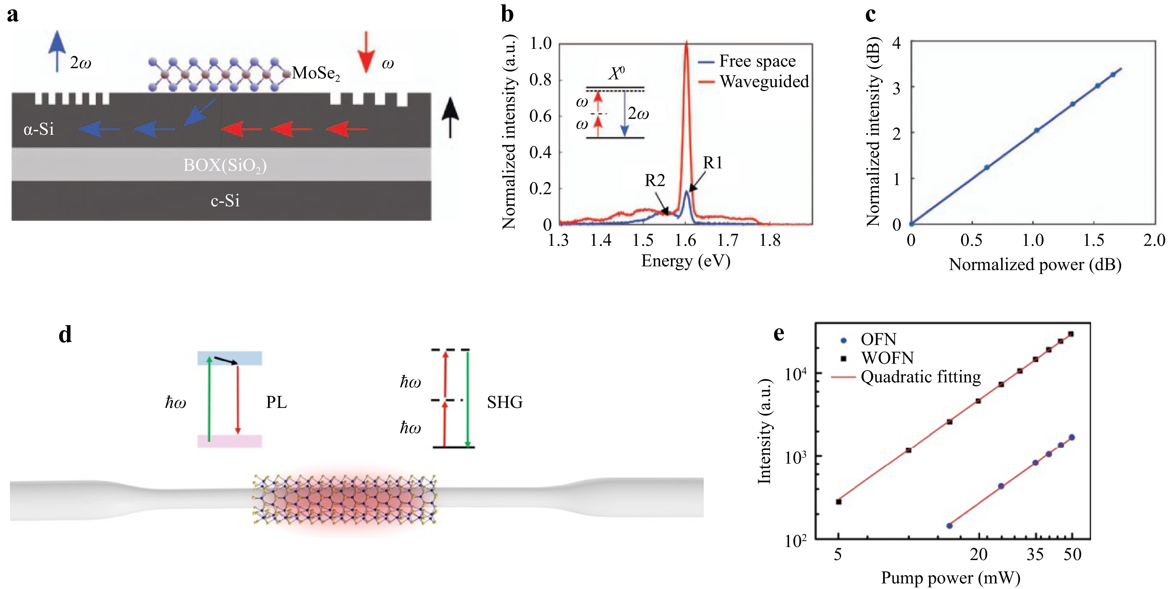
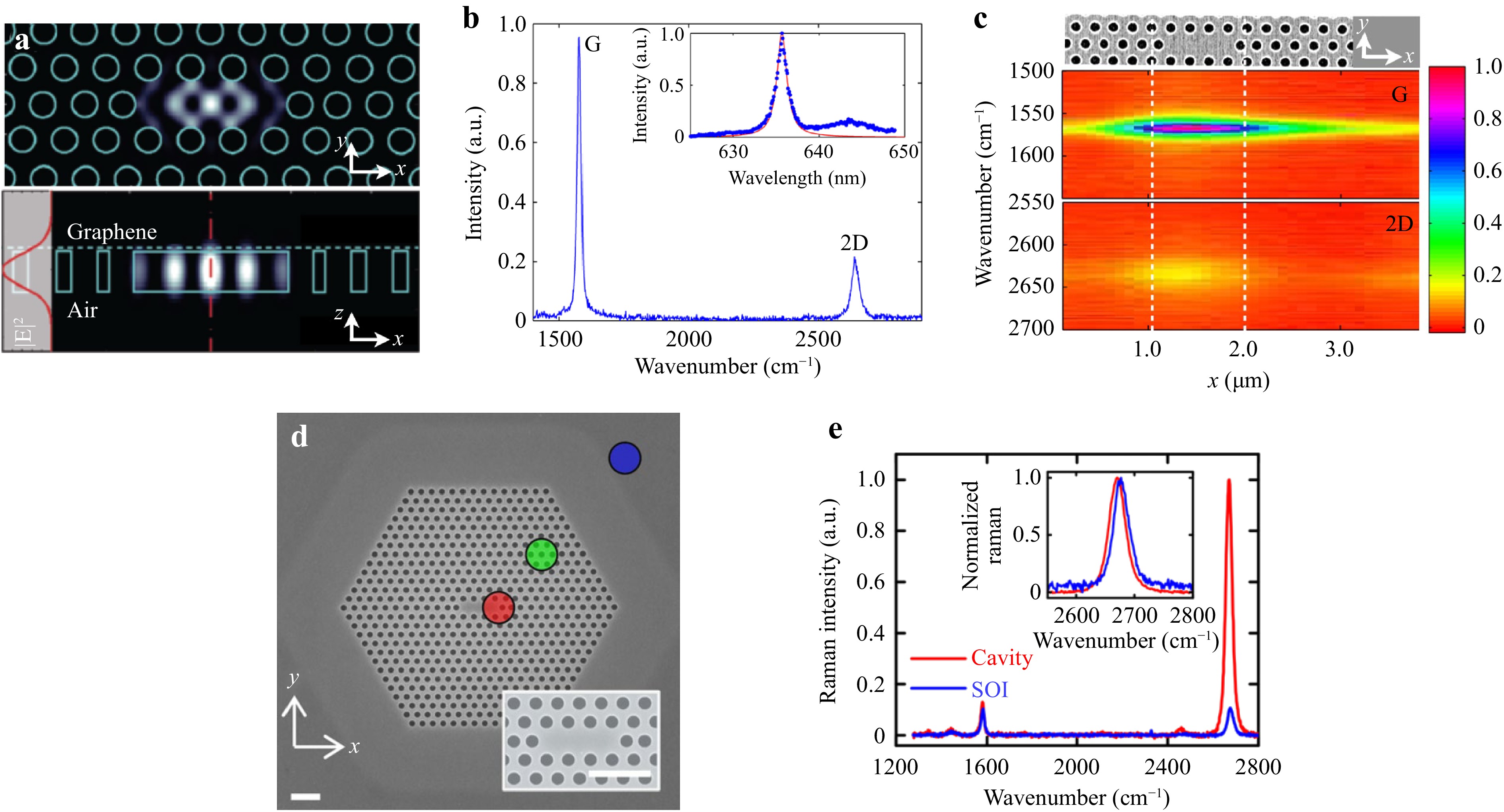
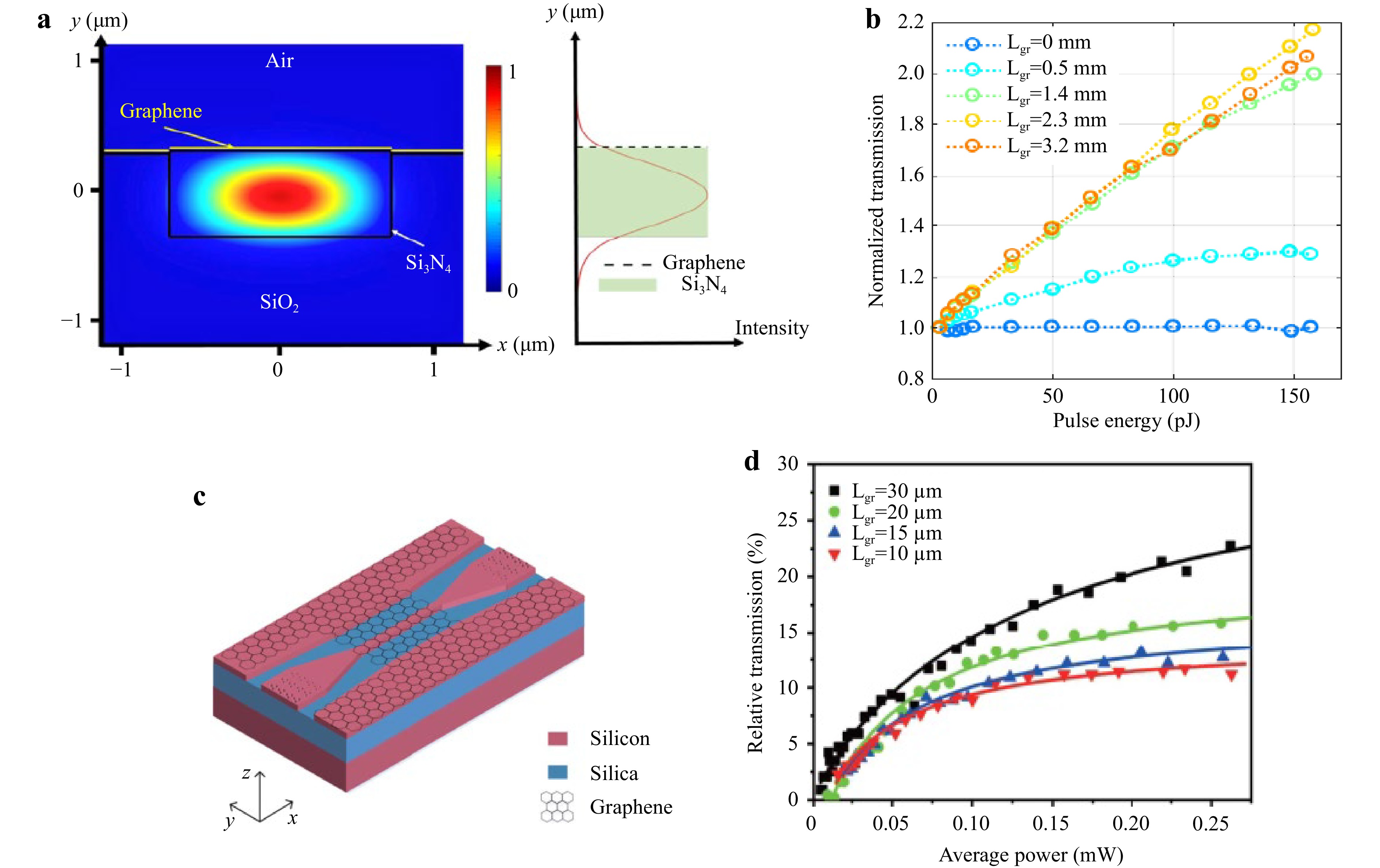
Interests surrounding the development of on-chip nonlinear optical devices have been consistently growing in the past decades due to the tremendous applications, such as quantum photonics, all-optical communications, optical computing, on-chip metrology, and sensing. Developing efficient on-chip nonlinear optical devices to meet the requirements of those applications brings the need for new directions to improve the existing photonic approaches. Recent research has directed the field of on-chip nonlinear optics toward the hybrid integration of two-dimensional layered materials (such as graphene, transition metal dichalcogenides, and black phosphorous) with various integrated platforms. The combination of well-known photonic chip design platforms (e.g., silicon, silicon nitride) and different two-dimensional layered materials has opened the road for more versatile and efficient structures and devices, which has the great potential to unlock numerous new possibilities. This review discusses the modeling and characterization of different hybrid photonic integration structures with two-dimensional materials, highlights the current state of the art examples, and presents an outlook for future prospects.

 Email
Email RSS
RSS