-
In recent years, metal halide perovskites have become well-deserved “star” materials among various semiconductors owing to their excellent optoelectronics properties1–5, such as high photoluminescence (PL) quantum yield (QY), high absorption coefficient, tuneable bandgaps, long carrier diffusion lengths, and high defect tolerance, thereby attracting considerable attention from both academia and industry. Consequently, perovskite optoelectronic devices6–9 such as solar cells, light-emitting diodes (LEDs), photodetectors, and lasers have been rapidly developed. For example, the power conversion efficiency (PCE) of the first organic-inorganic halide perovskite solar cell (PSC) reported in 2009 was only 3.8%10. Currently, the PCE of the state-of-the-art PSC exceeds 25%11. Such rapid progress is impressive because it took nearly 70 years for silicon solar cells to achieve similar PCE.
However, stability problem due to factors such as oxygen, moisture, heat, and light, is the main issue hindering the commercialisation of perovskite optoelectronic devices12. Although erosion caused by oxygen and moisture can be effectively avoided by hermetic packing, some light-induced detrimental phenomena are intrinsic to perovskites owing to their ionic properties. Properties such as ion migration13 and phase segregation14 cause the anomalous photocurrent density–voltage hysteresis in PSCs and deteriorate optoelectronic devices15. In addition, prolonged light irradiation leads to a strong coupling between photoinduced carriers and the perovskite lattice, thereby destroying perovskite films and forming degradation products16–18 because of the soft lattices19. However, in some special cases, the defect density of perovskite films can be effectively reduced by light soaking, resulting in improved PL intensities and lifetimes; this is known as the light-induced self-repairing effect20,21. Thus, the phenomenon of light–matter interactions in perovskites is complex and fascinating.
Integrating various optoelectronic devices onto a single chip is a crucial step in satisfying the requirements of advanced integrated optics and is poised to play a pivotal role in the development of next-generation information technology. Various micro-/nano-manufacturing techniques22–24 including photolithography, electron beam lithography, focused ion beam (FIB) lithography, direct laser writing (DLW), ink printing, and direct vapour-phase growth, have been developed to fabricate complex structures on perovskites to realise multiple functions. The achievable resolution of the fabricated microfeatures and variation in the crystal structure during fabrication have a direct impact on the performance of the final optoelectronic device. In practical applications, multiple factors such as manufacturing costs, processing efficiency, and scalability of production must be considered. For example, photolithography provides a high resolution of a few nanometres; however, the polar solvent and photoresist have a huge impact on the perovskites and damage the crystal structures because of their ionic properties and poor stability25. The fabrication processes using electron beam26 and FIB27 are highly precise; however, they are relatively inefficient and the equipment is rather expensive, which is challenging for mass production. Template-assisted vapour-phase growth is a bottom-up approach. Thus, single-crystalline perovskites can be directly grown on various substrates to form arrays, thereby preserving the crystal structure28. However, the resolution is low and depends on the template or the arrayed seeds.
DLW is based on the interaction between light and matter and is an efficient, contactless, mask-free, and depth-resolved micropatterning technique. It is typically performed by coupling a laser beam with a high-resolution microscope to minimise the output focal spot29,30. The resolution of DLW depends on the diameter of the output focal spot and threshold response of the material31,32. Due to the diffractive nature of light, the diameter of the laser focal spot is limited to 1.22 λ/NA, where λ is the wavelength of the laser and NA is the numerical aperture of the objective lens. Thus, a shorter wavelength and larger NA can result in a higher resolution. Depending on the fabrication mechanism and material threshold response, the best resolution is usually between a few and a few hundred nanometres. Furthermore, the DLW technique is scalable. The focused laser field can be changed into specific shapes, or multiple focal spots can be generated simultaneously using a spatial light modulator32–34, which considerably increases the fabrication flexibility, lowers the fabrication cost, and makes it suitable for large-scale production. Moreover, the processing laser can act as the excitation light for PL spectral measurements, which can be used to monitor the fabrication process.
DLW relies mainly on nonlinear processes, including multiphoton polymerisation, photon-induced ablation, and phase changes to enable three-dimensional (3D) fabrication35. Thus, an ultrafast laser with a high peak power is preferable. Femtosecond (fs) lasers are widely used in commercial systems for 3D printing and laser micromachining36,37. Recently, continuous wave (CW) lasers with low instantaneous power have also been used to fabricate patterns on perovskite microplatelets (MPs) and modify their crystal structures based on the thermal effect owing to the soft lattice of perovskites38. CW lasers are not only considerably cheaper than fs lasers, which lowers the requirement for equipment, but can also slightly process the surface of perovskite MPs to realise microencryption38. Similarly, the low formation energy (−7.09 eV for CsPbBr3)3 enables the in-situ nucleation and crystallisation of perovskite precursors under laser irradiation39,40. Even when the precursors are embedded in glass, the halide ions can migrate and form different crystal structures by modifying the laser power density, resulting in different emission wavelengths41,42. Therefore, owing to the ionic properties of perovskites, the DLW technique is extremely simple and efficient. Moreover, the research on DLW deepens the fundamental understanding on the interaction mechanisms between light and perovskites, paving the way for designing optoelectronic devices with improved performances.
In this review, we summarise the recent research progress in DLW on perovskites. In Section 2, the interaction mechanisms between laser and perovskite are divided into six categories: laser ablation, laser-induced crystallisation, laser-induced ion migration, laser-induced phase segregation, laser-induced photoreaction, and other laser-induced transitions. In Section 3, we focus on the applications of perovskites with micro-/nano-patterns and array structures, such as displays, optical information encryption, solar cells, LEDs, lasers, photodetectors, and planar lenses. The advantages of the patterned structures are highlighted. Finally, the current challenges for DLW on perovskites are discussed, and our perspectives on their future development are also presented.
-
A laser is an excellent tool for manipulating, fabricating, and processing nano/microstructures on semiconductors, with the unique advantages of high precision and contactless, easy, and mask-free operation. DLW based on different interaction mechanisms between lasers and perovskites have been developed owing to the special structure of perovskites. The detailed interaction mechanism sensitively depends on the laser properties, such as the wavelength, pulse/CW, power, and repetition rate, thereby providing a flexible and powerful tool for processing perovskites with precisely controlled nano/microstructures. The wide variety of interaction mechanisms indicates the considerable potential of DLW for various applications in microelectronics, photonics, and optoelectronics.
-
Since the 1990s, ultrafast lasers have emerged as effective tools for manipulating the structure of materials and have been widely applied in precision mechanical processing and micro-/nano-manufacturing30,43,44. The extremely high peak power and ultrashort pulse duration of ultrafast lasers allow for the direct ablation of material surfaces based on strong light-matter interaction-induced nonlinear absorption. Generally, laser ablation is a complex multiphysics process dominated by thermalisation45–47. Beginning with the rapid deposition of pulsed energy, electrons generated by multiphoton ionization are heated and transmitted to the lattice. The solid material is then melted into a superheated liquid via thermalisation. After breaking through the ablation threshold, the vaporisation of material leads to the formation of plasma and ejection of nanoparticles (NPs), forming a hole at the laser-focused spot and accomplishing the removal of materials. A schematic of the laser ablation mechanism of perovskites, referring to Kanaujia et al.48, is shown in Fig. 1a.
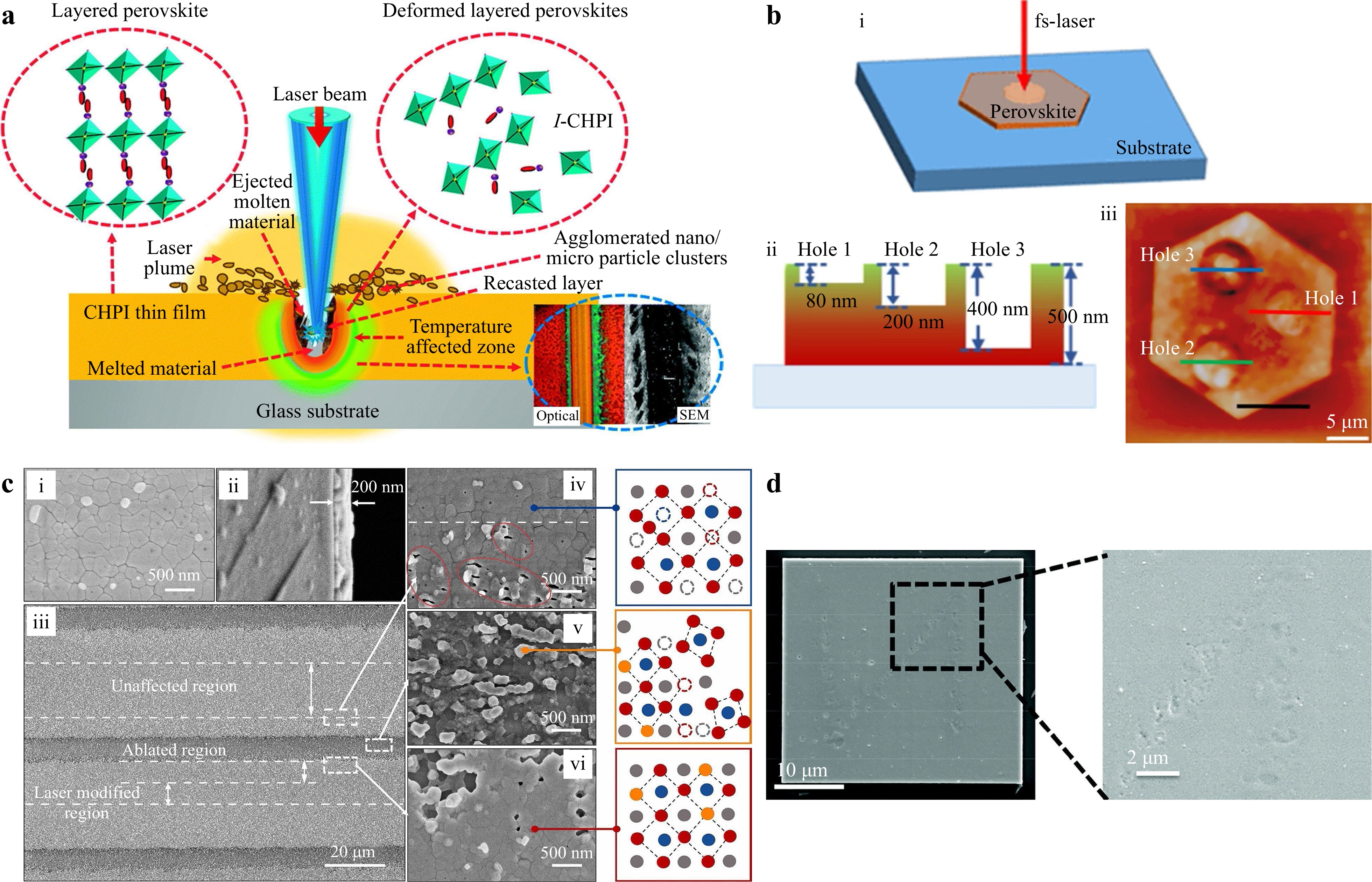
Fig. 1 a Schematic of laser ablation mechanism. Reproduced with permission48. Copyright 2016, Royal Society of Chemistry. b Schematic of i) DLW process, ii) three holes with different depths fabricated on NPs by DLW, and iii) corresponding atomic force microscopic (AFM) image of the DLW-processed perovskite NPs. Adapted with permission49. Copyright 2019, American Chemical Society. c Scanning electron microscopy (SEM) images of MAPbBr3 polycrystalline thin film (i) before laser ablation, (ii) from cross-sectional view, and (iii) and after laser ablation (iii); and (iv)-(vi) Magnified SEM images of corresponding dotted regions. Reproduced with permission53. Copyright 2023, Elsevier. d SEM images of a mild laser ablated CsPbBr3 MP (left) and the magnified image of the dotted region (right). Reproduced with permission38. Copyright 2021, Royal Society of Chemistry.
Ultrafast lasers have been extensively employed to fabricate precise microstructures of various perovskites based on ablation effects49–53. Owing to the high spatial resolution and reduced thermal influence of fs-DLW, micropatterns were fabricated on single perovskite nanoplatelets with gradient bandgaps (Fig. 1b)49. By controlling the processing depth, the perovskite nanoplatelets exhibited spatially resolved multicolour emissions. Rajan et al.53 investigated the fs-laser ablation effect on MAPbBr3 (MA=methylammonium) polycrystalline thin films (Fig. 1c); the ablation strip was divided into three regions: ablated, laser-modified, and unaffected. The agglomerated nano/microparticles at the edge of the laser-modified region significantly increased the local PL intensity and reduced the random lasing threshold by seven times owing to non-radiative defect passivation. Although the PL properties were enhanced at the boundaries of the microstructures, the resolution and quality of the microstructures were reduced by this residual debris. Therefore, a different structure in which the CsPbBr3 film was sandwiched between two layers of glass was introduced to avoid the ejection of debris during laser ablation52. By controlling the DLW parameters, such as the laser fluence and scanning speed, the materials in the ablated regions were completely removed. Consequently, the fabricated micropatterns exhibited high-quality and well-defined edges.
Unlike traditional DLW, a CW laser with a short wavelength is strong enough to ablate perovskites for micropatterning owing to the soft lattice of perovskite and its high absorption coefficient. This process is dominated by single-photon absorption38,48,54. For example, Kanaujia et al.48 successfully modified the optical and structural properties of two-dimensional (2D) layered inorganic-organic perovskites and shaped them into different sizes using a 410-nm CW laser. A prolonged processing time resulted in the accumulation of NPs at the boundaries along the laser tracks, leading to an improvement in the PL intensity. As reported in our previous work38, mild CW laser ablation can cause small dents in CsPbBr3 perovskite MPs (Fig. 1d), which have been proven to be significant for micro-encryption.
During the DLW process, the laser is focused on the substrate to achieve a high resolution for micro-manufacturing. In principle, the resolution of micropatterns fabricated by DLW is typically lower than those fabricated via traditional nano-manufacturing techniques using electron beam or ion beam lithography, and it is difficult to reach the subwavelength scale owing to the diffraction limit of the laser. To overcome this limitation, Liang et al.55 proposed regulatory focus ablation on perovskites by modulating the focal depth of the laser. The minimum width of the annular nanostructure reached 200 nm (Fig. 2a−c), which was one-tenth of the hole diameter at the focus. In this way, more precise micropatterns were fabricated on the CsPbBr3 films compared with the regular DLW process. However, this approach cannot fabricate perovskite arrays with subwavelength resolution, owing to the excessively ablated region around the annular nanostructure. Zhizhchenko et al.51 fabricated surface gratings on CsPbBr3 microcrystals by fs-DLW using a stripe-shaped laser beam (Fig. 2d). These microgratings were used as microlenses to focus the laser beam into a small spot with subwavelength resolution and increase the penetration depth (Fig. 2e), which was verified by finite-difference time-domain simulation results (Fig. 2f). A series of microstructures were successfully fabricated (Fig. 2g−i) by the irradiation of a polarised beam on the perovskite surface microgratings. However, this approach is limited by predesigned microgratings; thus, arbitrary micropatterns with subwavelength spatial resolution cannot be fabricated. Perovskite micropatterns fabricated by laser ablation possess high resolution and precise structures, which are widely applied in optoelectronic devices and advanced photonic applications. Further details are presented in Section 3.
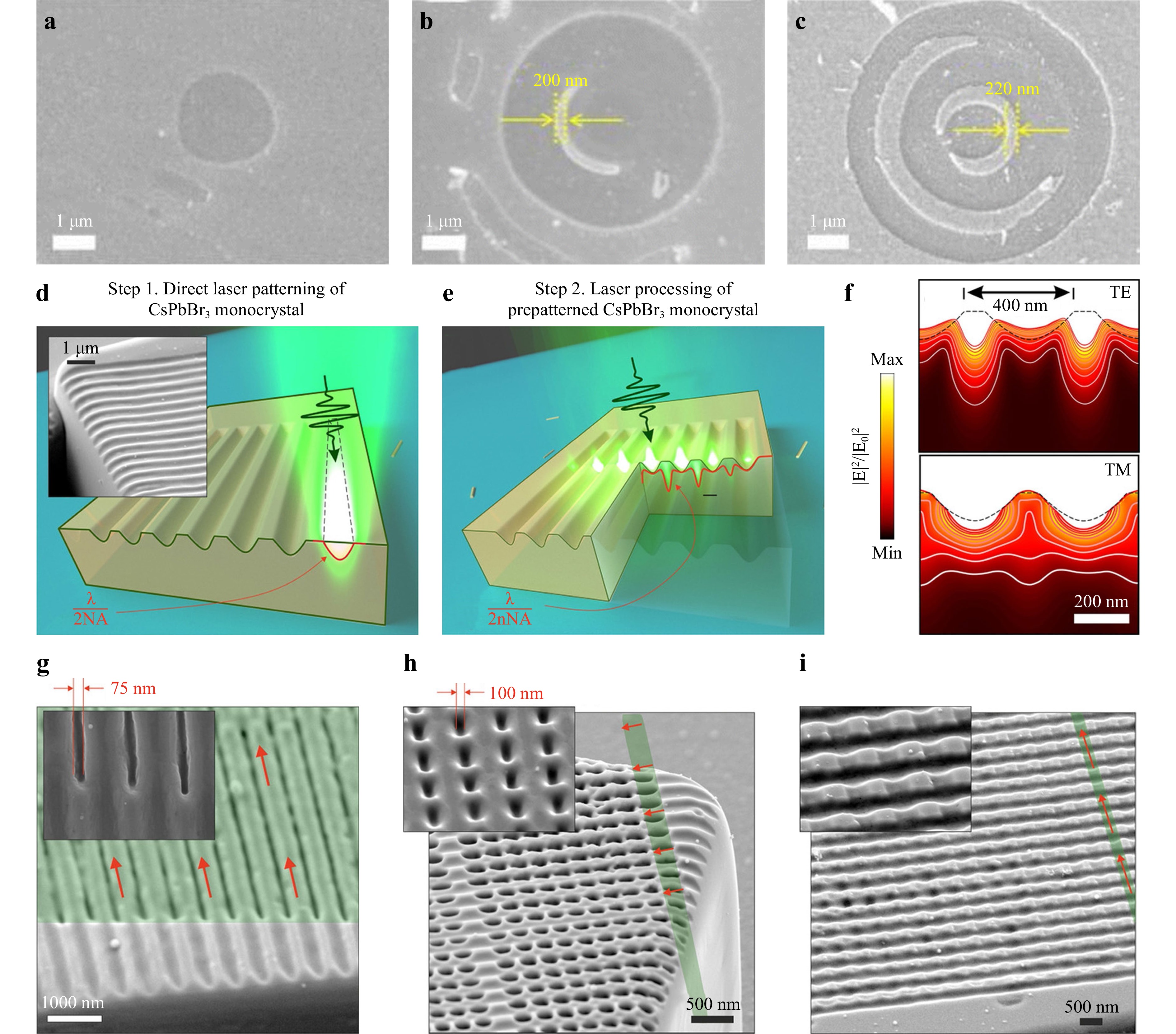
Fig. 2 a−c SEM images of micro-holes fabricated on perovskite films via fs-laser ablation at various focus depths. Reproduced with permission55. Copyright 2023, Royal Society of Chemistry. d Schematic of laser patterning process on CsPbBr3 micro-crystals using a stripe-shaped beam with a pitch of 400 nm. Inset: SEM image of the CsPbBr3 micro-crystals surface grating from a side-view51. e Schematic of the second step involving subwavelength laser patterning process, based on the focusing effect of surface micro-grating structures51. f Calculated squared electric-field amplitude |E(r, z)|2 during laser irradiation51. g−i SEM images of the patterned micro-structures on CsPbBr3 micro-crystals. Inset: corresponding magnified SEM images, presenting the subwavelength resolution. Reproduced with permission51. Copyright 2021, Wiley-VCH.
-
Perovskite precursors can be readily crystallised through the thermal effect of laser irradiation39,56–60 owing to their low formation energies and ionic properties. However, it is difficult to directly induce the crystallization of perovskite on transparent substrates using CW laser with relatively low instantaneous power density without heat accumulation. Therefore, cross-shaped platinum metal or Au/C thin films were deposited on a glass substrate as light absorption pads or layers to accumulate heat (Fig. 3a, b)56. The substrate was then immersed in the MAPbBr3 perovskite precursor solution and irradiated using a CW laser. By controlling the precursor concentration and DLW conditions, MAPbBr3 was crystallised in situ into arbitrary micropatterns. In contrast, fs-laser irradiation can directly induce localised heat accumulation on substrates owing to its high instantaneous power density. For example, Arciniegas et al.40 utilised a fs laser to directly irradiate perovskite precursors composed of N-methylformamide, PbBr2, and HBr on a Si substrate (Fig. 3c). The Si substrate was then selectively heated through light absorption, which in turn transferred heat to the liquid layer. The temperature of the irradiated spot was higher than that of the outer ring, generating a temperature gradient that led to the formation of smaller MAPbBr3 perovskite crystals in the inner region owing to the temperature-dependent nucleation-driven growth mechanism (Fig. 3d). By changing the DLW parameters, such as the laser power, stage displacement speed, and exposure time, the shape and size of the perovskite crystals can be controlled.
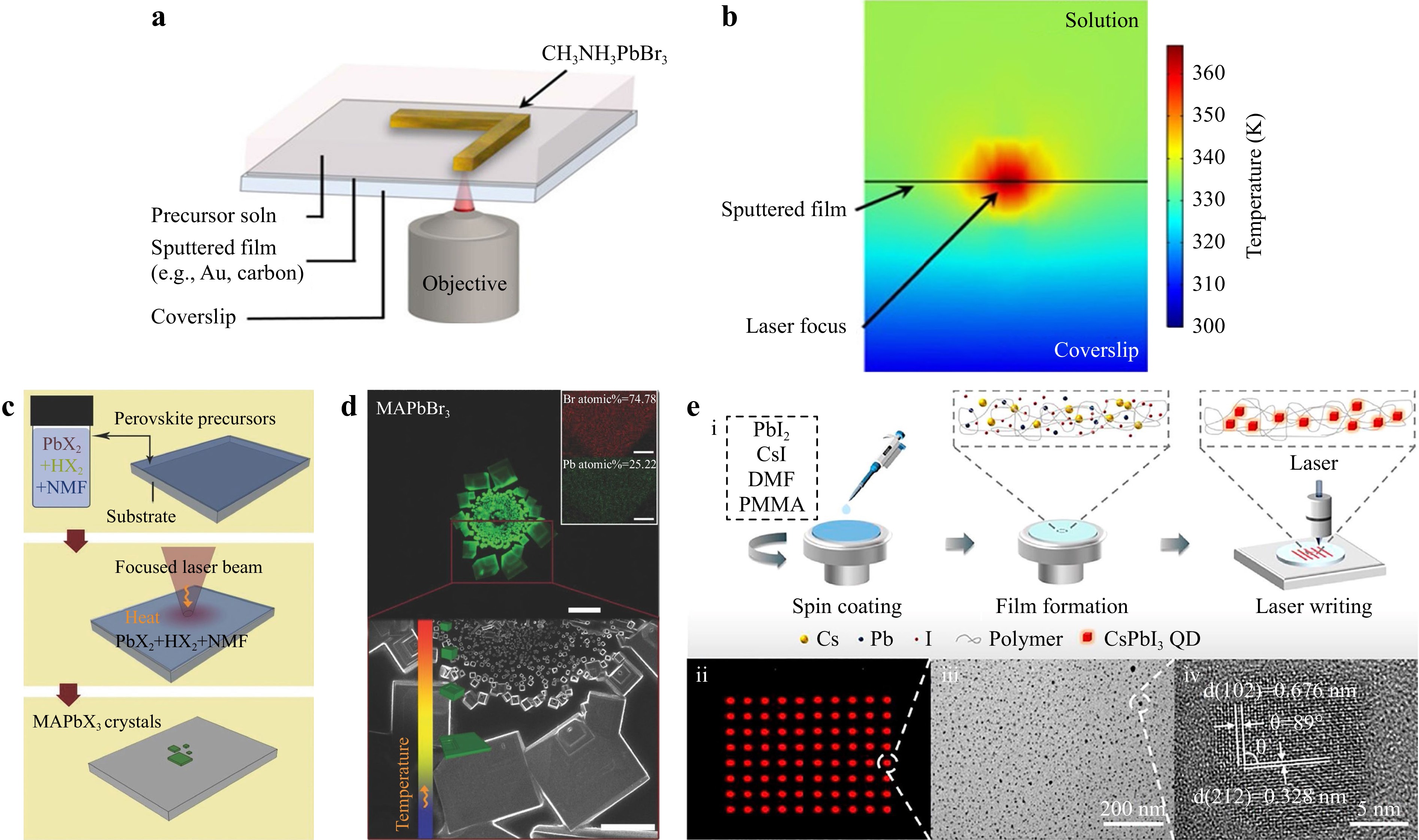
Fig. 3 a Schematic of the laser-induced crystallization of MAPbBr356. b Simulation of temperature distribution under 1-mW focused laser irradiation. Reproduced with permission56. Copyright 2016, American Chemical Society. c Schematic of DLW on perovskite precursors and formation of MAPbX3 crystals by the thermal gradient on a Si substrate40. d Fluorescence image of the formed MAPbBr3 crystals (upper), and SEM image (lower) of the red square region. The scale bars are 100 and 50 μm, respectively. Inset: corresponding halide elemental mapping, and the scale bars are 2 μm. Reproduced with permission40. Copyright 2017, Wiley-VCH. e i) Schematic of the fabrication process of CsPbI3 PQDs by DLW; ii) fluorescence image of the fabricated CsPbI3 PQD arrays; and corresponding (iii) TEM and (iv) HRTEM images of the CsPbI3 PQDs. Reproduced with permission59. Copyright 2021, American Chemical Society.
In most cases, laser irradiation-induced perovskites or micropatterns are directly exposed to the atmosphere, which suffer from the corrosion of moisture and oxygen in the environment, hindering further integration and transfer to different substrates. Zhan et al.59 reported the fabrication of γ-phase CsPbI3 perovskite quantum dot (PQD) micropatterns embedded in a polymeric matrix by 405-nm nanosecond laser writing on the precursors containing PbI2, CsI, dimethyl formamide, and polymethyl methacrylate (PMMA) (Fig. 3e). The PLQY of the resulting red-emitting CsPbI3 PQD micropatterns was 92%. By tuning the DLW parameters, the resolution of the linewidth reached 0.9 μm. Moreover, a fs laser with high pulse energy can directly induce the localised crystallisation of perovskite in glass. Micropatterns of CsPbBr3 PQDs were directly fabricated inside an oxide glass containing the precursor elements Cs, Pb, and Br by fs-laser irradiation57. Benefiting from the protection and high transparency of glass, the perovskite micropatterns possessed high stability against moisture and oxygen and exhibited bright fluorescence. Interestingly, the fluorescent patterns could be easily erased by further fs-laser irradiation because of the degradation of CsPbBr3 PQDs into PbBr2 and CsBr, which were subsequently recovered by thermal annealing (Fig. 4a). The laser-induced reversible formation and degradation of CsPbBr3 inside glass is crucial for information storage and security applications. Moreover, this technique is applicable to fabricating micropatterns of blue-emissive CsPb(Cl/Br)3 inside glass61. Owing to their cubic crystal structures, perovskite precursors preferably form MPs or cubic crystals under a relatively low laser power40,56, whereas the perovskites nanocrystals (PNCs) or PQDs are usually obtained under a high laser power with a strong thermal effect41,57.
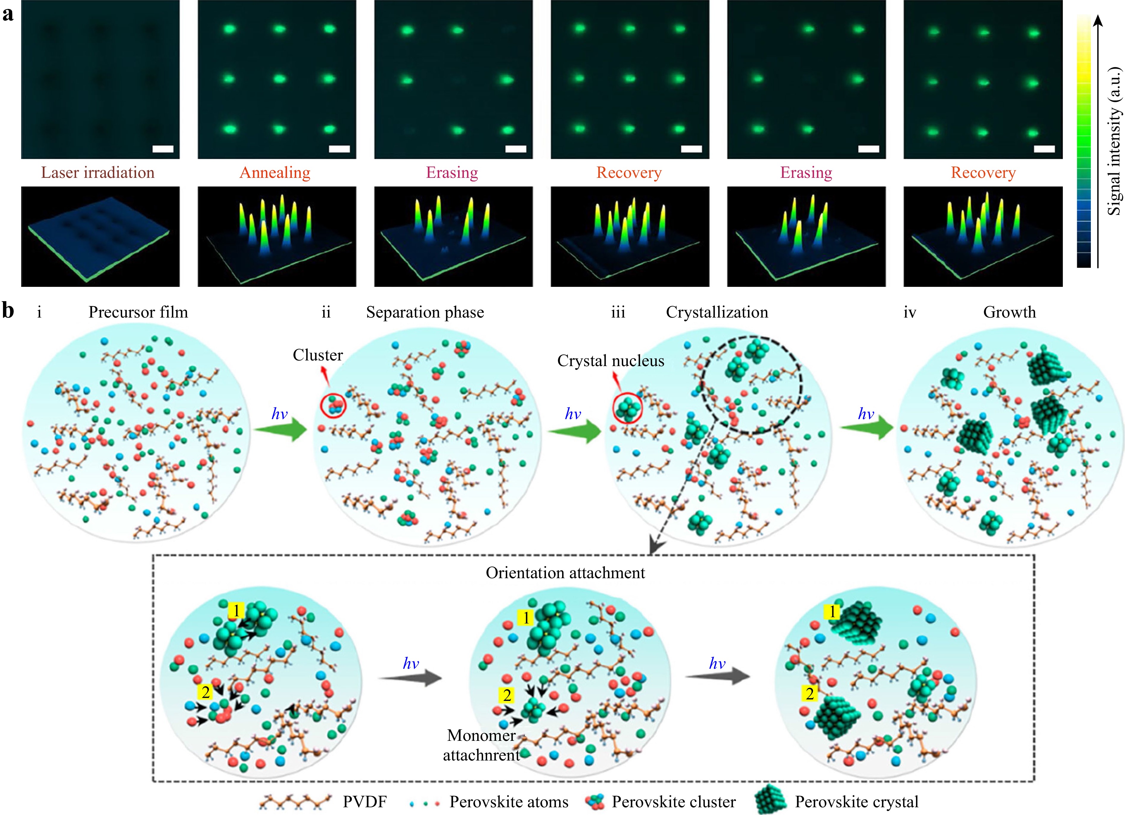
Fig. 4 a Fluorescence images (upper) and mapping images of readout signal intensity (lower) of CsPbBr3 PQD arrays inside glass, during erasing–recovery processes. All the scale bars are 100 μm. Reproduced with permission57. Copyright 2019, Springer Nature. b Schematic of the laser-induced formation mechanism of CsPbBr3 NPs inside a PVDF matrix. Reproduced with permission60. Copyright 2023, American Chemical Society.
It should be noted that the thermal ablation effect induced by ultrafast laser energy deposition usually generates undesirable crystallisation around the focused regions, affecting the resolution of micropatterns and damaging the crystal structures. Nie et al.60 reported the lossless CW-DLW of perovskite NPs inside a polyvinylidene difluoride (PVDF) matrix. This localised crystallisation was triggered by the photon absorption of the precursor film instead of the thermal ablation effect. In-situ TEM results indicated that the attractive van der Waals forces between the precursor complexes and polymer chains were suppressed owing to the electric field gradient generated by laser irradiation (Fig. 4b). After phase separation, crystallisation, and growth of the perovskite precursor complexes, CsPbBr3 NPs were formed inside PVDF. Consequently, multicolour patterned films were successfully fabricated by DLW and were stacked into multiple layers.
-
Photocurrent hysteresis is commonly observed in organometallic PSCs62–64. Various speculations63 such as defect theory, ferroelectric properties, and ion migration have been proposed to explain this hysteresis. Among these, illumination-activated ion migration behaviour was evidenced to be a primary reason65. In most cases, ion migration is considered harmful to the performance and stability of optoelectronic devices63,66. In contrast, several reports have suggested that the PL intensity of perovskite films can be enhanced through ion migration, which is known as the light-induced self-repairing effect20,67,68. For example, Stranks et al.67 demonstrated that photoinduced electrons filled the traps of perovskite films and generated a localised electronic field, which removed the halide ions to fill the nearby vacancies, thus reducing the defect density and increasing the PL.
Mixed ionic-electronic conduction and ion migration behaviour are unique properties of halide perovskites among various semiconductors. Laser-induced PL variations owing to ion migration offer new opportunities for the patterning of fluorescent structures. During the laser processing of CsPbBr3 MPs, halide ions migrate away from the laser spot, accompanied by PL quenching. After the halide ions return to their original positions under dark conditions, the partial PL intensities recover38. The migration of halide ions embedded in glass can be controlled by altering the irradiation time of the fs laser41. Schematic of the laser-induced ion migration during the DLW process is shown in Fig. 5a. Briefly, the high temperature of the laser spot leads to liquid nanophase separation. Subsequently, Br-rich liquid perovskites are firstly formed owing to their smaller radius, lighter ionic weight, and a greater complexation between Pb2+ and Br− compared with I− ions. Driven by the chemical potential gradient, I− ions then diffuse to the Br-rich liquid perovskite region to replace the Br site, resulting in Br/I mixed phases. Therefore, a longer laser irradiation time results in a higher I content of the PNCs and a red shift in the PL wavelength (Fig. 5b, c). Furthermore, controlling the cation migration was also realised in CsCdxPb1−xBr3 PNCs glass system by varying the fs-laser irradiation time (Fig. 5d−f), exhibiting the analogous mechanism42. Interestingly, the stability and PLQY of blue-emitting perovskites were improved by the laser treatment. Therefore, stable multicolour micropatterns can be fabricated by DLW based on the ion migration mechanism.
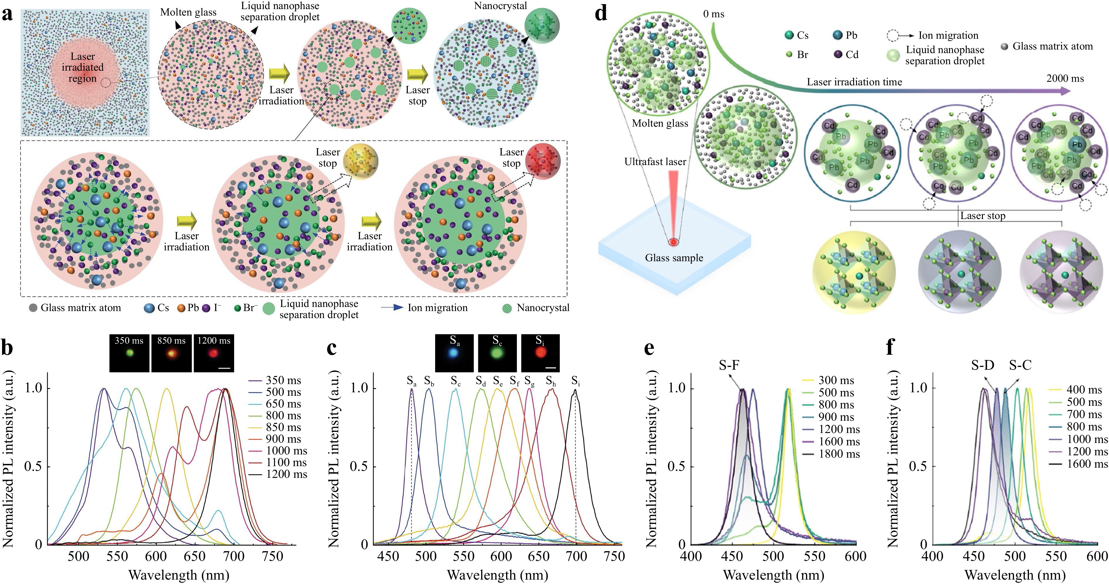
Fig. 5 a Schematic of the laser-induced ion migration and formation of CsPb(Br1−xIx)3 PNCs inside glass41. b, c PL spectra and PL mappings of CsPb(Br1−xIx)3 b and CsPb(Br1−xIx)3/CsPb(Br1−xClx)3 c PNCs obtained under various DLW process parameters. Reproduced with permission41. Copyright 2022, American Association for the Advancement of Science. d Schematic of the laser-induced ion migration and formation of CsCdxPb1−xBr3 PNCs inside glass42. e, f PL spectra and PL mappings of CsCdxPb1−xBr3 PNCs obtained under various DLW process parameters; laser repetition rates were 120 KHz e and 60 KHz f. Reproduced with permission42. Copyright 2023, Wiley-VCH.
-
Perovskite bandgaps can be conveniently manipulated through direct synthesis with different halide composites or by post-treatment with anion exchange. The coverage of the entire visible spectrum has significantly broadened their application in solar cells, LEDs, and full-colour displays69,70. However, these mixed-halide perovskites usually suffer from severe phase segregation, particularly in Br/I mixed systems, causing the degradation of perovskites and deterioration of the performance of optoelectronic devices14. For example, under laser irradiation or electric bias, Br/I mixed-phase perovskites separate into I-rich and Br-rich phase domains, accompanied by a redshift in the absorption wavelengths and PL emissions71–74. Various strategies such as trap passivation, crystallinity control, and A-site cation exchange have been developed to suppress the phase segregation of perovskites and improve phase stability14. Nandi et al.75 improved the phase stability of (FA)PbBr1.8I1.2 (FA=formamidinium) perovskites by substituting FA with 10% MA. The A-site cation exchange increased the activation energy for phase segregation and provided a higher energy barrier.
Currently, the proposed driving forces of phase segregation can be roughly divided into three typical mechanisms76–79, the Coulomb force, lattice strain, and thermodynamic processes. In the thermodynamic model79, the CsPb(BrxI1-x)3 system is stable when the change in Gibbs free energy (ΔG) is negative. Under light illumination, the strain energy increases, whereas ΔG changes from negative to positive, leading to phase segregation. Similar to light-induced ion migration, Belisle et al.77 proposed photoinduced electron trapping by the surface defects of perovskites, which generated a localised electric field and separated the halide ions based on the Coulomb force. In addition, the illumination of perovskites leads to the formation of polarons because of the strong coupling between the photoinduced carriers and lattices, causing lattice distortion. Subsequently, the halide ions are separated by the release of lattice strain energy76.
Phase segregation can be used to create multicolour micropatterns or microheterojunctions in single-crystalline perovskites for on-chip integration. Thus, DLW based on light-induced phase segregation has been used to pattern mixed-halide perovskites. Wang et al.80 proved that vacancy defects are the main pathway for halide ion migration on CsPb(BrxI1-x)3 MP surfaces and proposed the concept of fabricating colourful micropatterns by DLW based on phase segregation. In our previous work81, we reported that the phase segregation process of CsPb(BrxCl1-x)3 MPs was dependent on their structural heterogeneity. Phase segregation readily happened on the heterogeneous CsPb(Brx/Cl1−x)3 MPs, whereas it almost disappeared on the homogeneous CsPb(Brx/Cl1−x)3 MPs with a higher crystallinity and lower defect density (Fig. 6a, b. We revealed that the direction of halide ion migration was closely related to the distribution of defects, allowing the fabrication of micropatterns by the introduction of defects via DLW. As shown in Fig. 6c, after the fabrication of defective micro-patterns, Br− ions migrate to the patterned defects and form Br-rich phases with green emissions under laser irradiation, exhibiting green micro-patterns on blue background.
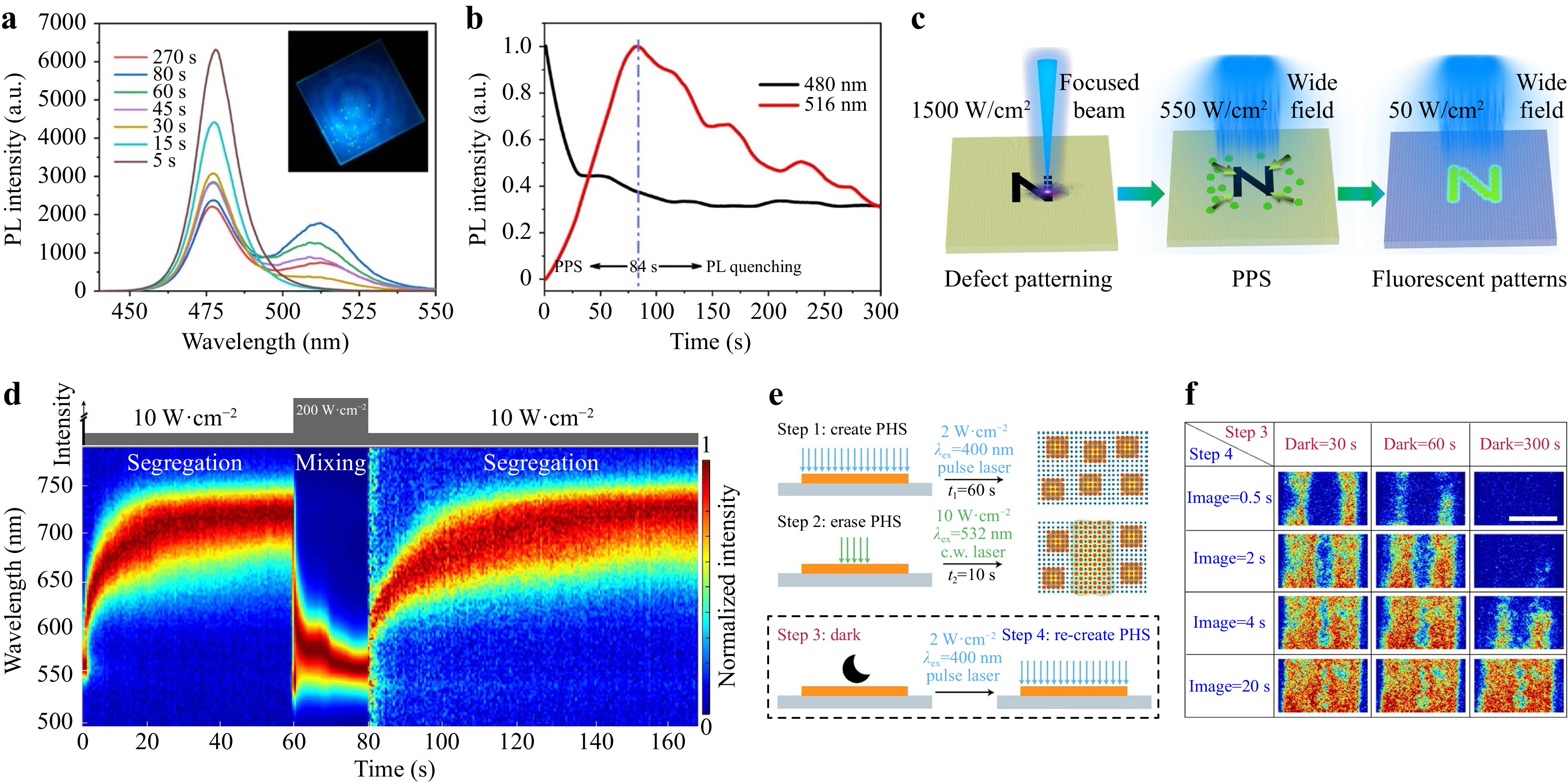
Fig. 6 a PL spectra of a heterogeneous CsPb(Brx/Cl1−x)3 MP during continuous laser irradiation. Inset: corresponding fluorescence image of the perovskite MP after laser irradiation for 80 s81. b PL intensities of the CsPb(Brx/Cl1−x)3 MP versus laser irradiation time81. c Schematic of DLW on CsPb(Brx/Cl1−x)3 MPs by manipulating phase segregation. Reproduced with permission81. Copyright 2022, American Chemical Society. d Normalized PL spectra of a MAPb(Br0.8I0.2)3 MP excited by a pulsed laser with various power densities82. e Schematic of write–read–erase processes on MAPb(Br0.8I0.2)3 MPs under various DLW parameters82. f Time-dependent confocal images of MAPb(Br0.8I0.2)3 MPs in the spectral window of 610–700 nm under various dark storage and laser scanning times. The scale bar is 5 μm. Reproduced with permission82. Copyright 2020, Springer Nature.
Phase segregation is moderately reversible, enabling write–read–erase processes. Mao et al.82 reported that phase segregation occurred in MAPb(Br0.8I0.2)3 MPs at the laser power density of 10 W/cm2, resulting in an emission shift from approximately 550 to 710 nm. Interestingly, the separated phases returned to their initial mixed phases at the high laser power density of 200 W/cm2 (Fig. 6d). Therefore, write–read–erase processes could be performed on the MAPb(Br0.8I0.2)3 MPs by DLW (Fig. 6e, f). Particularly, separated phases were created on perovskite MPs by laser scanning (2 W/cm2) over the entire crystal, and a focused laser (10 W/cm2) was used to irradiate specific regions to generate partial halide-ion mixing. Thus, micropatterns that could be used to store information were formed. This information could be conveniently read under wide-field light illumination. After storage in the dark, all information was erased and next writing could be performed. In other words, the separated phases inevitably recovered their initial state within a few minutes in the dark, implying that information could not be stored for a long time. Recently, the slow recovery of the separated phases on MA0.17FA0.83Pb(I0.5Br0.5)3 thin films, lasting tens of hours, has attracted significant research interest83. In summary, controlling the phase segregation and recovery processes not only provides deep insight into their photophysical processes but also guides the fabrication of colourful micropatterns on perovskites by DLW.
-
Traditional photolithography techniques have been extensively applied to fabricate microstructures on semiconducting electronic components to meet the demands of on-chip integration. This technology is primarily based on the photochemical reactions of photoresists under the ultraviolet (UV) light illumination84. In negative photoresists, crosslinking or polymerisation occurs upon light exposure, whereas decomposition occurs in positive photoresists. However, perovskites are unstable in polar solvents and easily dissolve in nonpolar solvents because of their ionic nature. The photoresist solution, developer, and chemical etchant cause significant damage to the perovskite films during the photolithography process. Therefore, the traditional photolithography technology is incompatible with perovskites.
To solve this problem, several groups have coupled photosensitive ligands with perovskites to make them act as “photoresists”, which has considerably simplified the photolithography procedures and protected perovskites from solvent corrosion85–88. Schematic of conventional photoresist-based photolithography and ligand-assisted direct photolithography (direct optical patterning) are shown in Fig. 7a85. The native ligands of the PNCs (oleic acid and oleylamine) are exchanged with polymer ligands of ammonium halide-terminated poly(2-cinnamoyloxyethyl methacrylate). Under UV irradiation, the ligands are polymerised owing to the cross-linking of the cinnamoyl C=C bond, forming a denser encapsulation layer to resist corrosion by the solvents and keep the PNCs stable. Subsequently, the PNCs located in the mask-covering regions are washed with toluene, leaving the patterned arrays85. Furthermore, Liu et al.87 directly added the photocrosslinker bis(fluorophenyl azide) (bisFPA) to PNC solutions. Under UV light, cross-linking occurred between the native alkyl ligands and the bisFPA of the adjacent PNCs through covalent bonding (Fig. 7b). Therefore, the non-crosslinked PNCs could be easily washed with toluene. The native ligands of the PNCs were well-preserved without deteriorating their PL performance during the direct optical patterning process. Consequently, the LEDs fabricated by these patterned PNCs possess the luminance of over 20,000 cd m−2 and external quantum efficiency of 6.8%. Fig. 7c shows the photopolymerization reactions between the trimethylolpropane tris (3-mercaptopropionate) and triallyl isocyanurate monomers under UV light. The reaction of the thiolene free radical is catalysed by PbBr2 complexes88. In contrast to direct patterning on spin-coated PNC films, perovskite precursor films are patterned first and then grown in situ into MAPbBr3 PQD arrays after annealing, which completely prevents damage to the PQDs during the direct optical patterning process. Thus, the patterned PQDs possessed a high resolution of 2450 pixels per inch with good stability and fluorescence uniformity.
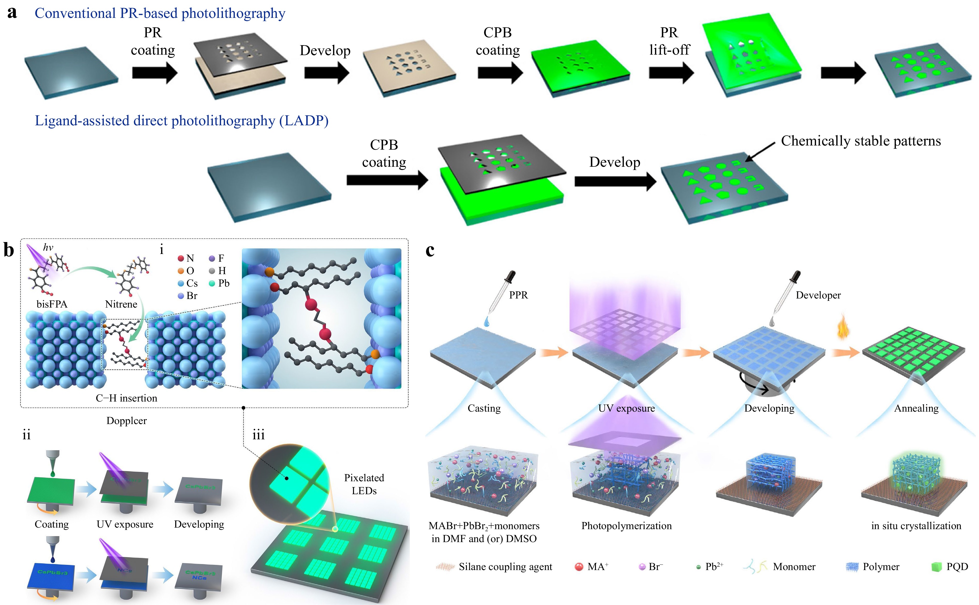
Fig. 7 a Schematic of conventional PR-based photolithography and ligand-assisted direct photolithography processes. PR = photoresist, CPB = CsPbBr3. Reproduced with permission85. Copyright 2021, American Chemical Society. b Schematic of (i) ligand cross-linking mechanism, (ii) direct optical patterning on PNCs, and (iii) applications in pixelated LEDs. Reproduced with permission87. Copyright 2022, American Association for the Advancement of Science. c Schematic of the photolithography on perovskite precursors based on the photopolymerization of monomers. Reproduced with permission under Creative Common CC-BY license88. Copyright 2022, Springer Nature.
Notably, the resolution of the above patterns is strictly limited by the mask. The fabrication of high-resolution masks requires elaborate micropatterning techniques, such as electron beam lithography, which is considerably expensive. DLW can be used to efficiently induce localised photoreactions directly on perovskites and form patterns without a mask. As shown in Fig. 8a, the ligands of the PQD films can be easily removed by 405-nm focused CW laser irradiation89. After immersion in the solvent, the treated regions of the PQD films remain attached to the substrate, whereas the untreated regions are easily removed (Fig. 8b), resulting in green-emissive micropatterns. Martin et al.90 embedded CsPbBr3 PNCs in polymer matrices containing iodododecane (Fig. 8c−e). Under UV laser irradiation, iodododecane decomposed into I− sources. Subsequently, selective patterns with red or green emissions were fabricated by the localised anion exchange between I− and CsPbBr3 PNCs during the DLW processing. The resolution of the patterned lines was approximately 15 μm, which is comparable to the direct optical patterning techniques. However, appropriate photosensitive materials that can release halide ions while being harmless to perovskites are still lacking. Moreover, internal anion exchange continues after DLW, which may break the fabricated micropatterns or structures70. Benefiting from the scalability of DLW, the combination of a UV laser with photosensitive materials to induce localised photoreactions on perovskites is a promising approach for realising arbitrary patterns with multicolour emissions, which significantly improves manufacturing efficiency and reduces costs.
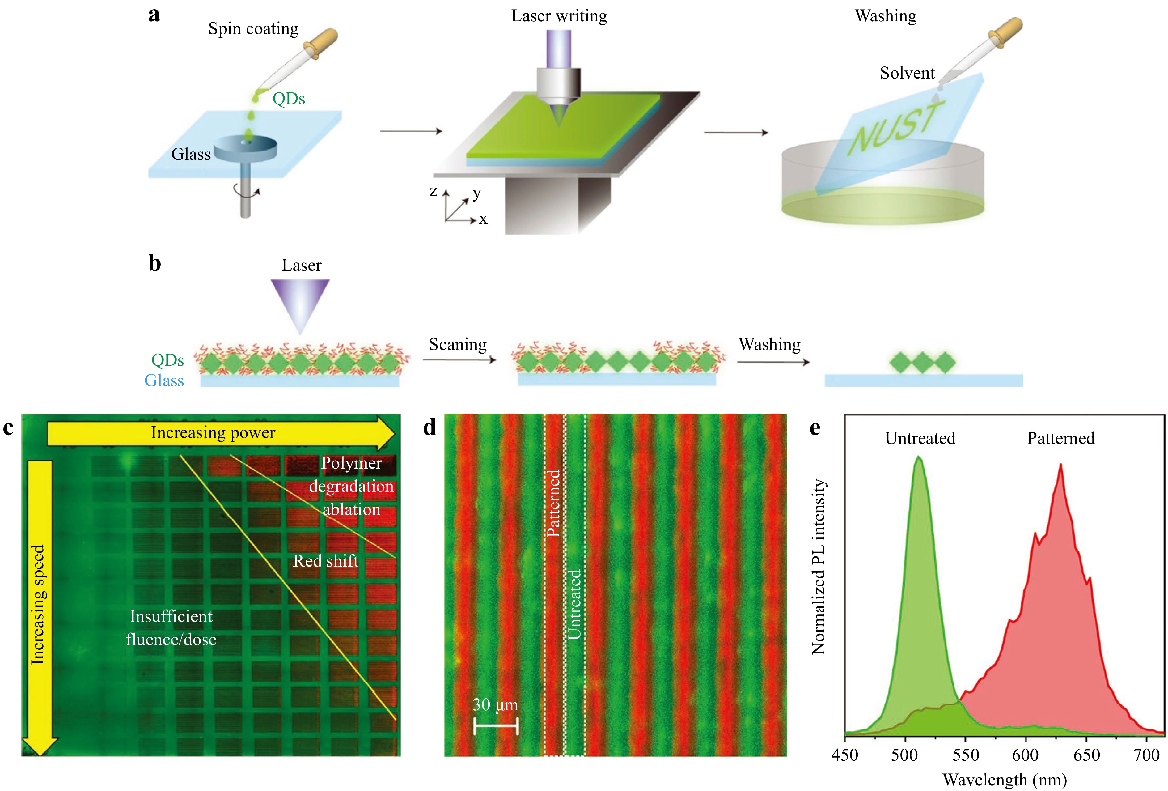
Fig. 8 a, b Schematic of DLW on PQD films a and the corresponding mechanism b. Reproduced with permission89. Copyright 2017, Wiley-VCH. c Example of operating windows with various emission wavelengths fabricated by varying the laser patterning parameters90. d High-resolution x-y-λ imaging of the patterned line tracks90. e PL spectra of perovskite polymer matrix with and without laser irradiation. Reproduced with permission90. Copyright 2022, Wiley-VCH.
-
In addition to the aforementioned mechanisms, other photoinduced transitions have been proposed for DLW. Compared with the non-perovskite δ-phase (yellow-phase) of FAPbI3, the α-phase (black-phase) of FAPbI3 possesses excellent optoelectronic properties, such as the narrow bandgap, which has been widely applied in solar cells91. However, the α-phase of FAPbI3 easily transforms into the undesired δ-phase of FAPbI3 even at room temperature, hindering the performance of solar cells. Therefore, it is necessary to transform the undesired δ-phase into α-phase92,93. Steele et al.94 reported that the 458-nm CW-laser irradiation is an effective way to promote the phase transition from δ-phase to α-phase FAPbI3 perovskites due to surface restructuring by laser-induced thermal effects. Photoinduced phase transitions provide a potential application for DLW.
When the connectivity between adjacent lead-halide octahedra changes, perovskites of various dimensions can be obtained95–97. The photo-induced dimensional transition offers a unique mechanism for DLW on perovskites. As shown in Fig. 9a, the femtosecond laser directly melts the CsPb2Br5 single crystals (SCs) in the irradiated regions owing to the thermal effect. Subsequently, the localised atoms rearrange during the cooling process, leading to the formation of CsPbBr3/CsPb2Br5 composites. Therefore, CsPbBr3 PNCs with bright green emissions are formed in millimetre-scale non-luminescent CsPb2Br5 perovskite SCs by fs-DLW98. Interestingly, the PL of the micropatterns is reversible during the wetting/drying treatment, which further realises multimodal optical encryption. Similarly, in our previous work99, we directly prepared green fluorescent micropatterns on a blue background using a CW laser in Eu-based metal-organic framework (Eu-MOF)/Cs4PbBr6 composites based on the photochromic process from blue emissive 0D Cs4PbBr6 to 3D CsPbBr3. This photochromic process was attributed to the light-induced defect healing of 0D Cs4PbBr6 and transition from 0D Cs4PbBr6 to 3D CsPbBr3 induced by moisture (Fig. 9b). Consequently, different patterns of blue and green emissions were successfully fabricated by DLW (Fig. 9c).
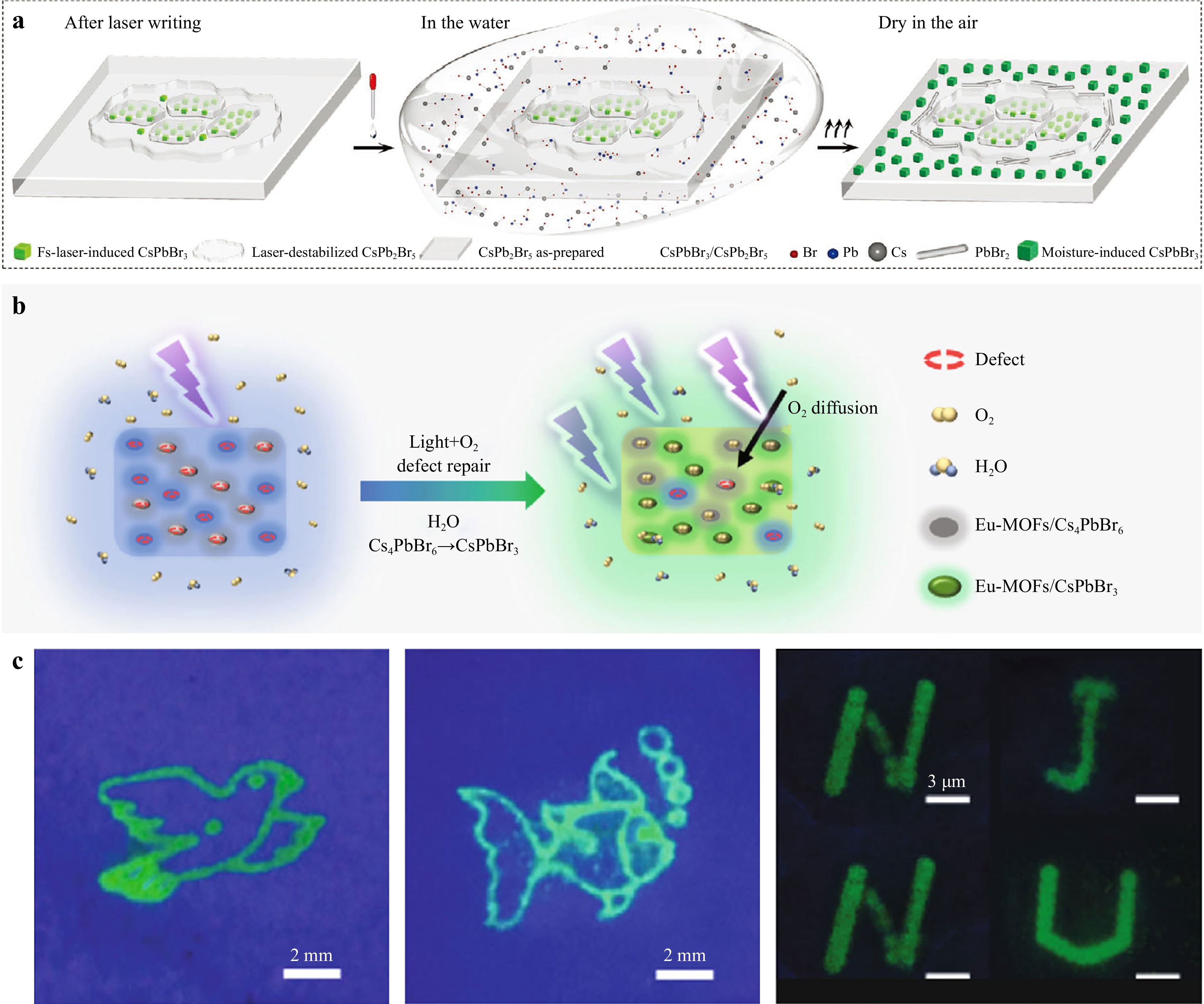
Fig. 9 a Schematic of the degradation and formation processes of CsPbBr3 inside the fs-laser-irradiated CsPb2Br5 SCs during water treatment. Reproduced with permission98. Copyright 2022, Wiley-VCH. b Schematic of the photochromic process of (Eu-MOFs)/Cs-Pb-Br composites99. c Different patterns obtained by DLW. Adapted with permission under Creative Common CC-BY 4.0 license99. Copyright 2022, The Authors.
-
The micropatterns of perovskites fabricated by laser ablation possess a high resolution of a few micrometres and produce colourful emissions, making them very suitable for high-quality displays. Liang et al.100 fabricated vivid micropatterns on 2D perovskite films by altering the DLW parameters (Fig. 10a, b). Furthermore, a QR code with high resolution is shown in Fig. 10c. However, patterned information can be easily read using an unencrypted microscope. To solve this problem, we developed a mild DLW technique based on 405-nm CW laser38. Mild CW laser irradiation caused only slight damage to the surface of the CsPbBr3 MPs, resulting in a fluorescence intensity contrast between the laser-processed spot and untreated regions. The fabricated micropatterns were only observable using a microscope with a selective fluorescence band and could not be observed using a common optical microscope, thereby realising information encryption38. Furthermore, full-colour micropatterns and 3D microhelix arrays were fabricated by Sun et al.41 based on the fs-DLW of perovskites inside glass (Fig. 10d). The fs-laser-induced erasing/recovery of blue-emissive PNCs packed in glass is also suitable for optical information encryption (Fig. 10e, f)61. Similarly, Nie et al.60 used a CW laser to induce perovskite crystallisation inside a PVDF matrix to avoid thermal ablation by DLW. The information represented by different patterns was invisible under the optical and scanning electron microscopes but could be decrypted under UV light excitation, realising information encryption (Fig. 10g). Li et al.98 realised multidimensional optical information encryption by fabricating CsPbBr3 PNCs micropatterns at various depths of CsPb2Br5 SCs by fs-DLW (Fig. 10h). The encrypted information was read in a similar way using a fluorescence microscope when excited with UV light. Unlike other designs, during different water treatment times, the fluorescent micropatterns gradually changed, realising space-resolved and time-resolved optical information encryption.
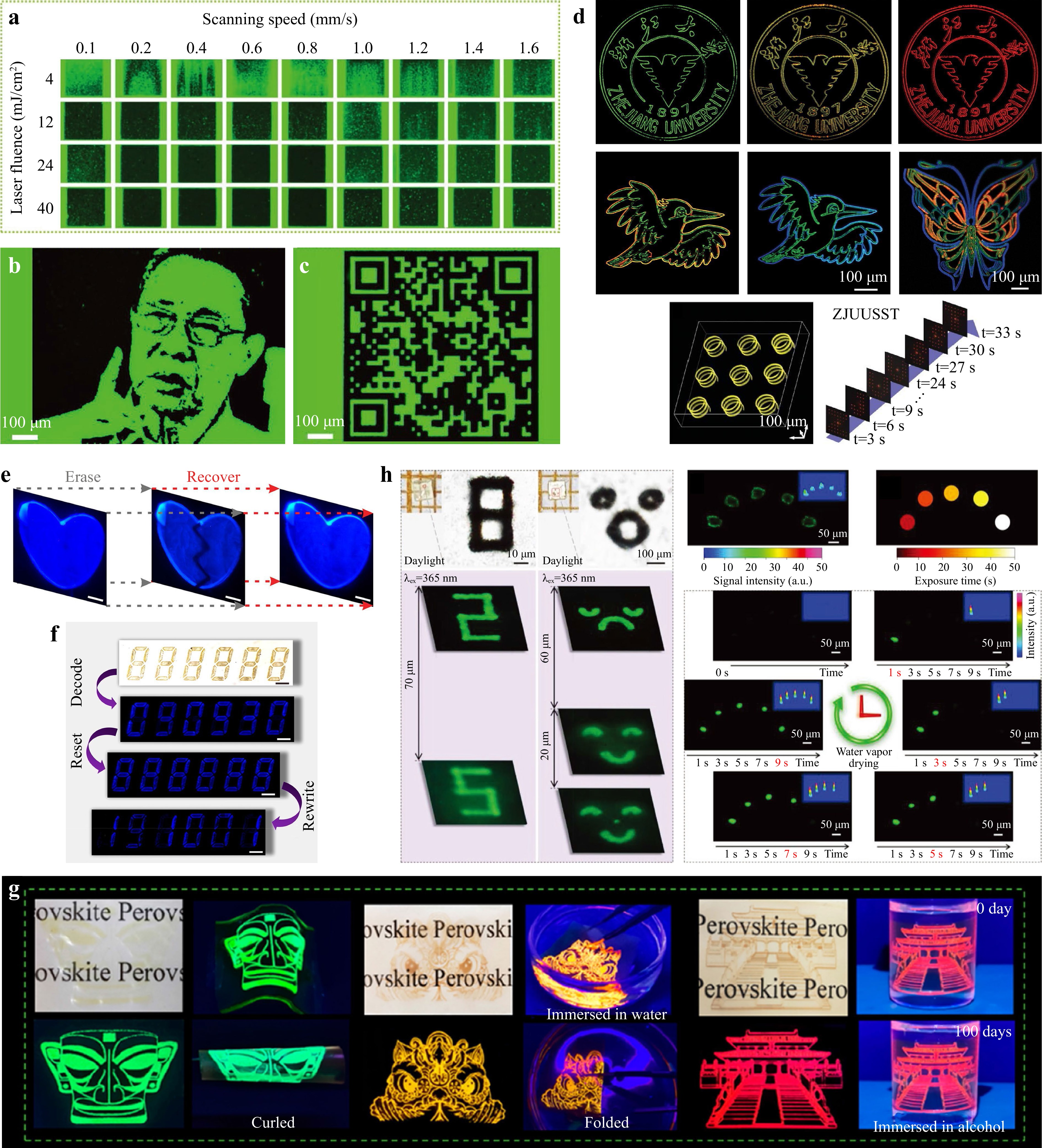
Fig. 10 a−c Fluorescence images of different 2D perovskite micropatterns, a 100 μm × 100 μm squares, b portrait of Mr. Nan-Shan Zhong, and c a QR code, fabricated by DLW. Reproduced with permission100. Copyright 2022, Wiley-VCH. d Fluorescence images of multicolour micropatterns and 3D microhelix arrays of CsPbX3 PNCs with various halide compositions inside glass. Reproduced with permission41. Copyright 2022, American Association for the Advancement of Science. e Fluorescence images of micropatterns showing switchable PL during the laser induced erasing/recovery process. The scale bars are 100 μm61. f Information encryption and decryption processes based on the erasable CsPb(Cl/Br)3 PNC micropatterns inside glass. The scale bars are 200 μm. Reproduced with permission61. Copyright 2020, American Chemical Society. g Different patterns based on flexible perovskite film under sunlight and UV irradiation. Reproduced with permission60. Copyright 2023, American Chemical Society. h Multi-dimensional information encryption based on the variable PL of CsPb2Br5 SCs induced by moisture and DLW. Reprinted with permission98. Copyright 2022, Wiley-VCH.
-
Perovskite films formed by laser-induced crystallisation have a high crystal quality, which is promising for applications in high-performance solar cells. Jeon et al.39 spin-coated perovskite precursors on a conducting substrate, and then used a near-infrared laser to induce the fast crystallization of MAPbI3 perovskites. The performances of solar cells were evaluated (Fig. 11a−c); typically, a maximum PCE of 11.3% was achieved by controlling the laser power density. A laser beam was applied to induce the crystallisation of the perovskite films, and the thermal gradient served as a driving force for the growth of larger grains (Fig. 11d)101. The structure of the solar cell is shown in Fig. 11e. The PCE of the optimised solar cell was 20.98% (Fig. 11f). Furthermore, the process was efficient and suitable for large-scale production. White light illumination can also induce defect reduction in FA(Cs,MA)PbI(Br)3 perovskites by driving excessive halide ions into the film bulk102, similar to the photoinduced healing effect. Consequently, the FA(Cs,MA)PbI(Br)3 PSC exhibited a high PCE of 20.1% with an open-circuit voltage of 1.053 V. To meet the demands of commercialisation, a single PSC is usually connected to PSC modules to improve the output voltage and reduce ohmic losses. Thus, during the fabrication of PSC modules, laser scribing techniques have been widely adopted for the preparation of interconnects owing to their exceptional manufacturing speed and precision103.
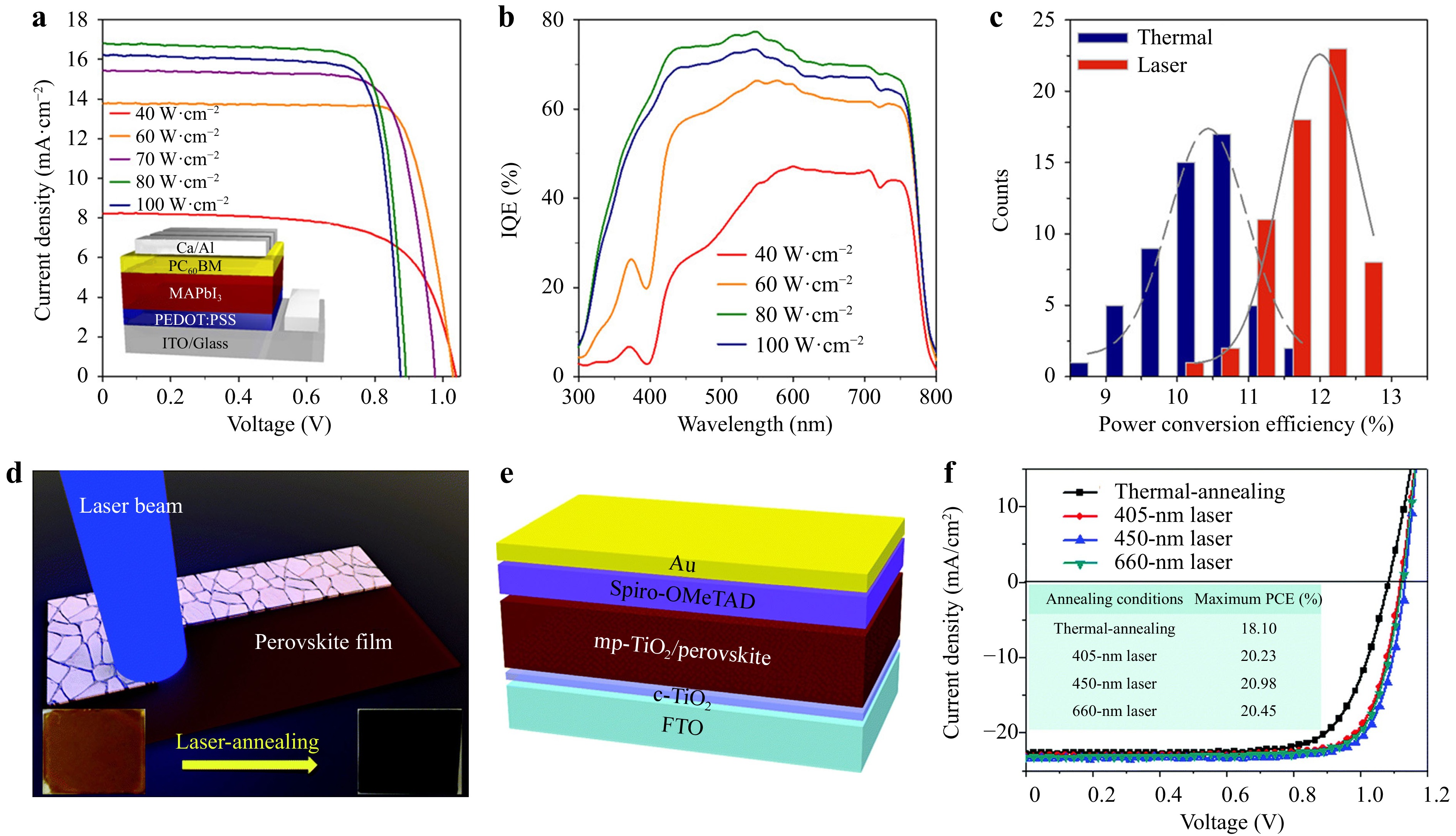
Fig. 11 a, b Current density–voltage characteristics a and internal quantum efficiencies b of PSCs fabricated using various laser power densities. Inset: schematic of solar cell architecture39. c PCE distribution of PSCs fabricated by thermal annealing and laser-induced crystallization. Reproduced with permission39. Copyright 2016, American Chemical Society. d Schematic of the laser-induced crystallization of MAPbI3 perovskite films. Inset: photos of perovskite films before (left) and after laser annealing (right)101. e Schematic of the PSC structure101. f Current density–voltage curves of PSCs fabricated under various annealing conditions. Inset: corresponding PCEs. Reproduced with permission101. Copyright 2020, Royal Society of Chemistry.
-
Micro-LEDs have attracted significant attention in both laboratory and industrial settings because of their superior luminance, wide colour range, and enhanced stability compared with conventional LEDs104,105. With the exception of the epitaxial growth technique, DLW is a high-throughput micropatterning technique that arranges perovskite films into tens of thousands of microscale pixels to meet the demands of micro-LEDs. The fs laser is an effective tool for ablating redundant parts to create micropatterns on a perovskite layer52. Liang et al. demonstrated an LED based on an arrayed perovskite with a maximum luminance and current efficiency of 18,390 cd/m2 and 1.9 cd/A, respectively52.
As mentioned above, DLW can be used to fabricate PNC micropatterns embedded in glass, and is also applicable to micro-LEDs. Hu et al.106 prepared CsPbBr3/CsPbBr2I PNC-embedded glasses with uniform green/red emission colours by heat treatment, and then used a fs laser to selectively destroy the PNCs to fabricate an inverted micropattern (Fig. 12a). Micro-LEDs were obtained by combining red or green emissive arrays of 7680 × 4320 pixels with a commercial blue LED screen. Moreover, by controlling the power density of the fs laser, PNC micropatterns embedded in glass were able to emit multiple colours ranging from green to red41. Then, a white micro-LED was fabricated by combining the emissive glass with a blue LED array41. The structures of the micro-LEDs based on the CsPbBr3 PNC microarrays are shown in Fig. 12b, c. This green LED exhibited a peak external quantum efficiency (EQE) of 6.8% with a luminance of more than 20,000 cd/m2 (Fig. 12d−f)87.
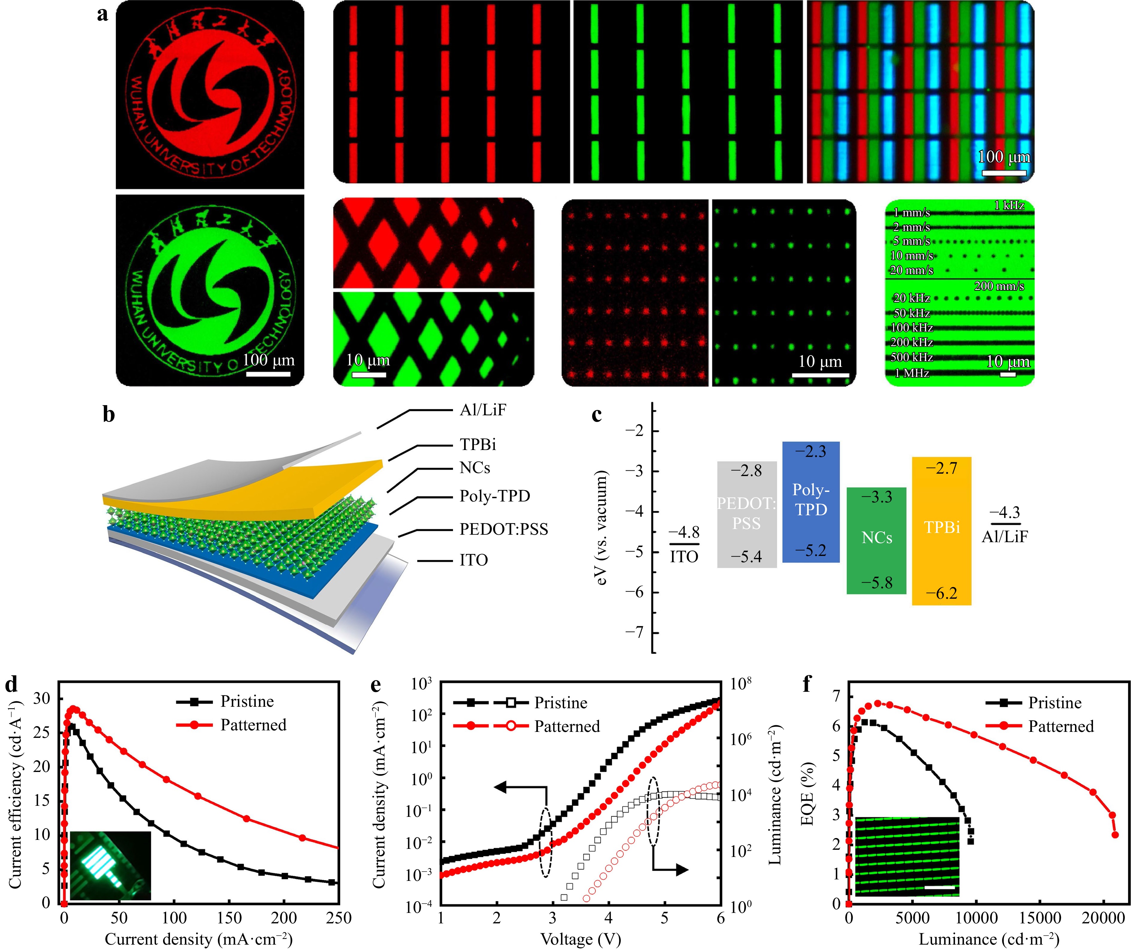
Fig. 12 a Fluorescent images of CsPbX3 PNC-embedded glass with different micropatterns and arrays fabricated by DLW. Reproduced with permission106. Copyright 2023, Elsevier. b Schematic of the LED architecture based on perovskite microarrays87. c Energy band diagram of the LED87. d−f Current efficiency–current density d, current density–voltage–luminance e, and EQE f characteristics of pristine and patterned devices. Inset: a photo of the working device d and an electroluminescent image of a pixelated LED f. The scale bar is 200 μm. Reproduced with permission87. Copyright 2022, American Association for the Advancement of Science.
-
The microstructure of a perovskite plays a crucial role in determining its lasing performance as it enables the perovskite to function as both a gain material and an optical cavity, allowing stimulated emission to be amplified107–109. In addition to directly grown perovskite SCs, the DLW technique is an efficient method for shaping perovskites into various geometries. To date, several groups have reported remarkable stimulated emission performance of perovskites with microstructures. For example, the output Gaussian-shaped laser pulse was shaped into a donut-shaped optical vortex beam to directly fabricate microdisk arrays on MAPbBrxIy perovskite films, which considerably increased the micro-manufacturing efficiency (Fig. 13a)110. The diameters of micro-disks were tuned from 2 to 9 μm. In addition, the perovskite micro-disk served as the whispering gallery cavity, possessing high quality single-mode lasing with quality factors of 5500; the optimal lasing threshold was 7 μJ/cm2 when pumped by a fs laser. The FAPbI3 perovskite microdisks were also fabricated by combining fs-laser writing and thermal co-evaporation. A low laser threshold of 3 μJ/cm2 was obtained111. Zhizhchenko et al.112 directly wrote gratings with a period of 260 nm on CsPbBr3 nanowires (NWs) via ablation using a focused stripe-shaped fs laser beam (Fig. 13b, c). The optical properties of the untreated samples were preserved. Based on the nanograting structure, the stimulated emission was outcoupled with the upper face of the NW at a small divergence angle of approximately 2°. The output laser exhibited excellent monochromaticity with a narrow wavelength-width of 0.08 nm, which was significantly narrower than that of the pristine NW without nanograting (0.18 nm).
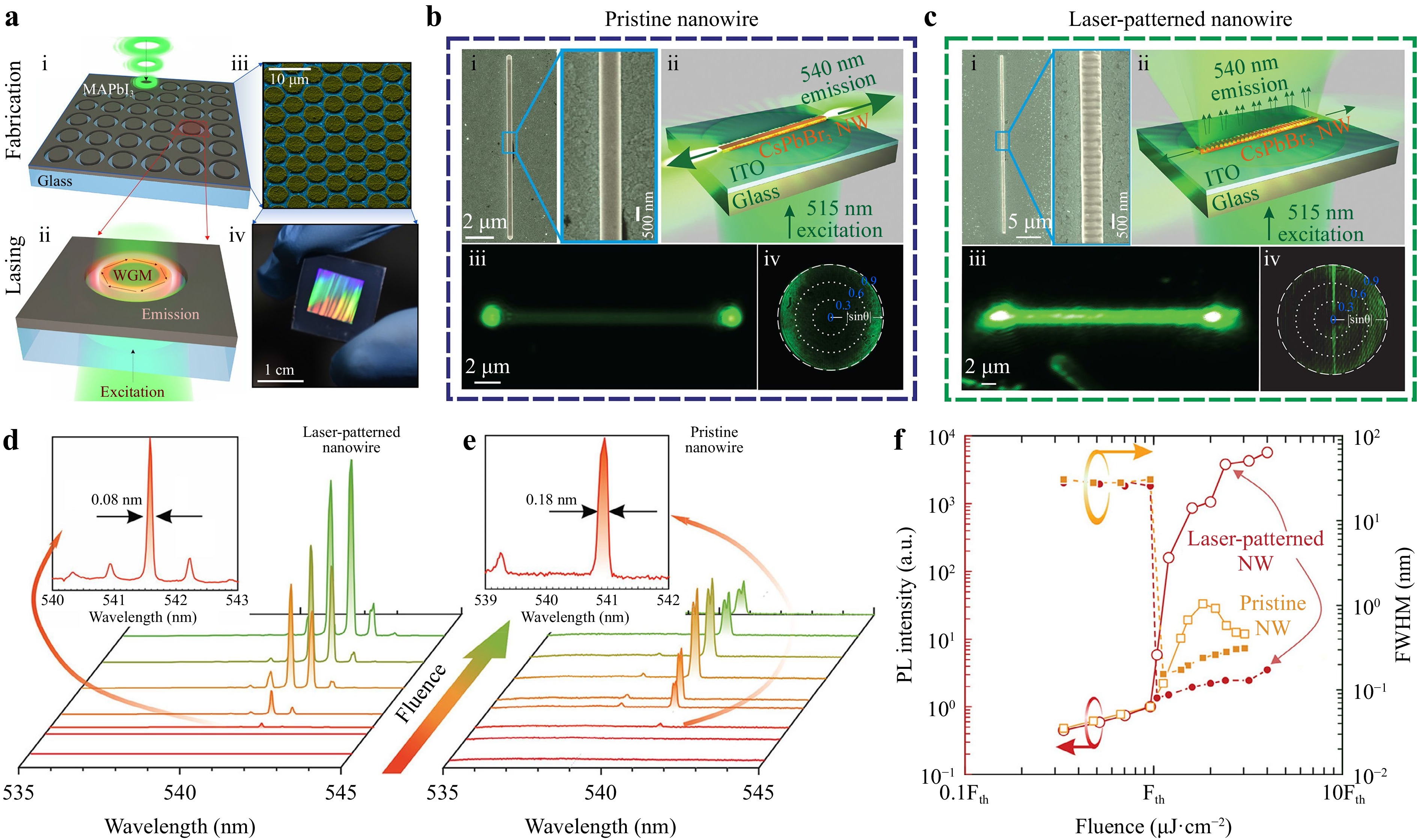
Fig. 13 a Schematic of perovskite microdisk arrays fabricated by DLW (i), and their lasing behaviour (ii). SEM image (iii) and photograph (iv) of the perovskite microdisk arrays. Reproduced with permission110. Copyright 2019, American Chemical Society. b, c SEM images (i), lasing schematic (ii), PL image (iii), and Fourier-plane image (iv) of pristine b and laser-patterned CsPbBr3 NWs c112. d, e Emission spectra of laser-patterned d and pristine e CsPbBr3 NWs under various pumping fluences. Inset: A magnified view of the main emission peaks112. f Emission intensity and FWHM of the main lasing peak versus pumping fluence for pristine and laser-patterned NWs. Adapted with permission112. Copyright 2021, American Chemical Society.
-
Microscale photodetectors typically exhibit high sensitivity and low energy consumption, making them highly desirable for integration into various devices113,114. DLW plays an important role in fabricating perovskite-based photodetectors. For example, Chou et al. fabricated a microphotodetector by the laser-induced crystallisation of a perovskite wire on a microelectrode array. The resulting device exhibited an excellent on/off ratio56. MAPbBr3 wires and MPs synthesised by DLW were used in photodetectors (Fig. 14a)40. These photodetectors achieved a maximum responsivity of 0.83 A/W in the range of 400–500 nm (Fig. 14b). Furthermore, perovskites obtained by laser-induced phase transition and anion exchange exhibited excellent photodetection performances115,116.
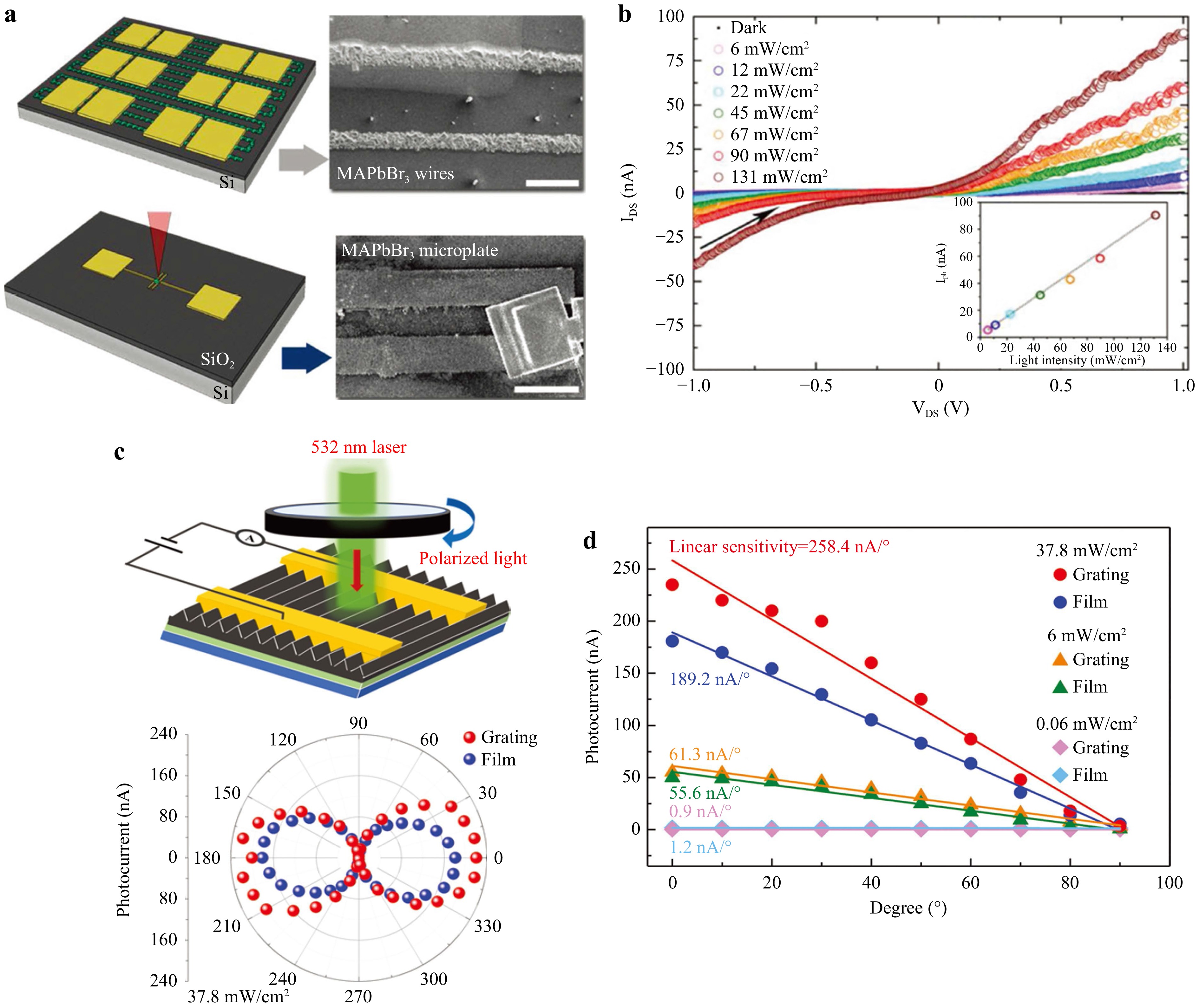
Fig. 14 a Schematic of two photodetector configurations and corresponding SEM images of photodetectors based on MAPbBr3 microwires and microplates fabricated by laser-induced crystallization. The scale bars are 50 μm (top) and 20 μm (bottom), respectively40. b I–V curves of MAPbBr3 micro-plate photodetectors under various illumination intensities. Inset: photocurrent versus applied light power at a bias of 1 V. Reproduced with permission40. Copyright 2017, Wiley-VCH. c Schematic of perovskite grating photodetector for polarization photodetection (upper), and the photocurrent versus polarization angle (lower) of perovskite triangular grating and film photodetectors at 5-V bias under the illumination intensity of 37.8 mW/cm2117. d Photocurrent versus polarization plot of perovskite triangular grating and film photodetectors under various illumination intensities. Reproduced with permission117. Copyright 2022, Wiley-VCH.
A periodic structure usually results in a significant enhancement in light absorption by modulating the distribution of the refractive index, which is significant for photodetectors. Tian et al.117 fabricated triangular microgratings on FAPbI3 perovskite films by fs-laser ablation. The period and depth of the micrograting were controlled by the power of the fs laser. The micrograting structure led to a high absorption intensity, low reflectance, and a significant enhancement of the PL intensity (67 times). Under a bias of 5 V and an illumination intensity of 30 mW/cm2, the photodetectors based on microgratings exhibited a responsivity of 11.7 A/W and detectivity of 7.8 × 1012 cm·Hz1/2/W, and the photocurrent reached 290 nA; these values were several times larger than those of the controlled devices. Moreover, these photodetectors were able to resolve the polarisation (Fig. 14c, d). In addition, laser patterned perovskite wafers also present considerable potential for the detection of high-energy rays, such as X-ray and γ-ray118,119. For example, a ring trench was fabricated on the Au electrodes of CsPbBr3 γ-ray detectors by DLW. These photodetectors exhibited the lateral leakage current of 60 nA at 10 V and mobility-lifetime product of 9.7 × 10⁻⁴ cm2/V118.
-
The low thermal conductivity of perovskites effectively inhibits the excessive thermal influence and removal of materials during the DLW process, thereby enabling precise control over the resolution of microstructures while maintaining good crystallinity. This makes perovskites excellent candidates for planar lenses. For example, Wang et al.120 fabricated concentric ring structures on 2D perovskite nanosheets by fs-laser DLW. As demonstrated in Fig. 15a−c, when incident light passes through the lens, it is focused into a 3D spot, with variations in amplitude and phase resulting from the different refractive indices of the media. Furthermore, changes in both the perovskite nanosheet composition and thickness lead to variations in the optical constants, such as the refractive index and absorption coefficient. Consequently, manipulating the amplitude and phase of the incident light varies the focal spot from 0.5 to 0.9 λ. However, for this Fresnel zone-plate planar lens, further increasing the number of rings and aperture diameter is difficult because the fabrication of edge lines with widths shorter than the subwavelength is limited by the resolution of the DLW technique. To this end, Yang et al.121 designed perovskite nanocrystal ultrathin planar (PUP) lenses based on the detour phase method, allowing for the flexible adjustment of the linewidth by controlling the DLW parameters. Consequently, the PUP lenses exhibited excellent resolution of the 3D focus spot and exceptional imaging capability. These pioneering works on the fabrication of planar lenses on perovskites by DLW have paved the way for new photonic applications, which are important for the development of more advanced photonic devices.

Fig. 15 a, b Schematic of light focusing through a 2D perovskite lens with concentric rings structure, viewed in 3D a and its cross-section b120. c Schematic of light transmission through an atomically thin material (blue plane) and air interface (green plane). Reproduced with permission120. Copyright 2020, Wiley-VCH.
-
The use of DLW techniques presents a promising pathway for the successful integration of flexibly designed microstructured and nanostructured perovskites onto individual chips. The DLW technique considerably speeds up the manufacturing efficiency owing to its facile operation process and high throughput compared with conventional semiconductor fabrication techniques, which are promising for the large-scale fabrication of complex micropatterns with high resolution. DLW is based on different laser–perovskite interaction mechanisms, which are categorised into the laser ablation effect, laser-induced crystallisation, laser-induced ion migration, laser-induced phase segregation, laser-induced photoreaction, and other laser-induced transitions. These mechanisms not only provide deep insights into the intrinsic ions or carrier dynamics in perovskites during laser processing but also provide guidelines for designing high-performance optoelectronic devices. Therefore, laser-induced patterns, microstructures, and pixel arrays have significantly promoted the application of perovskites in optoelectronics such as displays, optical information encryption, solar cells, LEDs, lasers, photodetectors, and planar lenses. State-of-the-art advances in optoelectronic applications are also reviewed.
Cheaper and flexibly controllable fabrication lasers, together with the superior optoelectronic properties of perovskites, have significant application potential for DLW on perovskites122,123. Currently, it is still in its infancy, and a huge boom in both fundamental research and industrial demand is anticipated124. For the future development of DLW on perovskites, few crucial technical bottlenecks must be solved. The challenges and our outlook are as follows.
First, the resolution of the DLW technique on perovskites makes it difficult to reach subwavelength ranges because of the diffractive nature of light and the response of perovskites, which makes it inferior to state-of-the-art lithography techniques. Furthermore, the practical size of a single pixel is usually several times larger than the laser focal spot, which might be caused by the out-of-focus when processing into a deep depth, or the thermal conduction effect. For the former, the two-photon DLW technique may be useful for fabricating subwavelength structures. For the latter, optimising the DLW parameters, such as the short wavelength, ultrashort pulsed fs laser, and optical coupling system, is important to reduce the excessive ablation caused by heat.
Second, it is proposed that the laser-induced self-healing effect is caused by trap passivation, which enhances the PL intensity of the perovskite on the laser spot. The performance of perovskite optoelectronic devices significantly improves upon exposure to mild illumination (100 mW/cm2)20. However, in most cases, prolonged high-laser-power irradiation easily destroys the lattice structures of perovskites, leading to their degradation38,125. Therefore, the illumination conditions are the key factors that determine the enhancement or deterioration of perovskite optoelectronic properties. Extensively and controllably introducing self-healing to various perovskites can significantly enhance the optoelectronic properties and further improve device performance.
Third, although micropatterns fabricated by phase segregation show exciting results, the main issue is that most patterns are only retained for a few minutes. This stability is insufficient for several practical applications, and thus limits further exploration. Therefore, it is important to prolong the existing time of the segregated phases, although this remains a challenge. In addition, laser ablation-induced debris ejection should be avoided during the manufacturing process to improve the precision of the micropatterns. In addition to controlling the DLW processing parameters, various compact buffer layers can cover the perovskite layer to form sandwich structures and reduce debris ejection.
Finally, to satisfy the demands of wearable optoelectronics and integrated photoelectric devices, it is important to extend the micropatterning techniques to flexible substrates. Additionally, the transfer of micropatterns between different substrates should be explored. The applications of perovskites cover almost all optoelectronic and photonic areas, such as single-photon sources, micro/nano lasers, photodetectors, optical gates, optical communication, waveguides, and nonlinear optics. Thus, it is highly promising to construct and integrate photonic devices with various functions based on a single perovskite chip.126,127 An advantage of DLW is its flexibility in fabricating arbitrary structures on the same substrate. This provides the possibility of integrating all the demonstrated elements into one chip using the same fabrication technique.
-
This work was supported by the Natural Science Foundation of Shandong Province (ZR2021YQ32), Taishan Scholar Project of Shandong Province (tsqn201909117), National Natural Science Foundation of China (Nos. 61901222, 21802074, and 11604155), and Natural Science Foundation of Jiangsu Province (BK20190697).
Direct laser writing on halide perovskites: from mechanisms to applications
- Light: Advanced Manufacturing 5, Article number: (2024)
- Received: 20 July 2023
- Revised: 25 December 2023
- Accepted: 29 December 2023 Published online: 13 March 2024
doi: https://doi.org/10.37188/lam.2024.004
Abstract: Metal halide perovskites have emerged as game-changing semiconductor materials in optoelectronics. As an efficient micro-/nano-manufacturing technology, direct laser writing (DLW) has been extensively used to fabricate patterns, micro/nanostructures, and pixel arrays on perovskites to promote their optoelectronic applications. Owing to the unique ionic properties and soft lattices of perovskites, DLW can introduce rich light–matter interactions, including laser ablation, crystallisation, ion migration, phase segregation, photoreaction, and other transitions, which enable diverse functionalities in addition to the intrinsic properties of perovskites. Based on their patterned structures, perovskites have numerous applications in displays, optical information encryption, solar cells, light-emitting diodes, lasers, photodetectors, and planar lenses, which are comprehensively discussed in this review. Finally, we discuss the challenges that must be addressed for the future development of this fascinating field.
Research Summary
Micro-/nano-manufacturing: Efficient laser writing on halide perovskites
In recent years, metal halide perovskites have emerged as game-changing semiconductor materials in optoelectronics due to their excellent optoelectronics properties. As an efficient micro-/nano-manufacturing technology, direct laser writing (DLW) has been extensively used to fabricate patterns, micro/nano structures, and pixel arrays on perovskites to promote their optoelectronic applications. Prof. Zhixing Gan from Nanjing Normal University, Prof. Baohua Jia from RMIT University, and colleagues now review the development of DLW on halide perovskites. The rich light–matter interaction mechanisms introduced by DLW including laser ablation, crystallization, ion migration, phase segregation, photoreaction, and other transitions, enable diverse functionalities in addition to the intrinsic properties of perovskites. Based on their patterned structures, perovskites have numerous applications in displays, optical information encryption, solar cells, light-emitting diodes, lasers, photodetectors, and planar lenses, which are comprehensively discussed in this review.
Rights and permissions
Open Access This article is licensed under a Creative Commons Attribution 4.0 International License, which permits use, sharing, adaptation, distribution and reproduction in any medium or format, as long as you give appropriate credit to the original author(s) and the source, provide a link to the Creative Commons license, and indicate if changes were made. The images or other third party material in this article are included in the article′s Creative Commons license, unless indicated otherwise in a credit line to the material. If material is not included in the article′s Creative Commons license and your intended use is not permitted by statutory regulation or exceeds the permitted use, you will need to obtain permission directly from the copyright holder. To view a copy of this license, visit http://creativecommons.org/licenses/by/4.0/.





 DownLoad: