


-
Complex lead halides with the perovskite structure and general formula APbX3 (A is a cation, either organic methylammonium (MA+) or formamidinium (FA+), or inorganic Cs+; and X is an anion of Br, Cl, or I) has been extensively studied in recent years in terms of radiation hardness. Many researchers found surprisingly high resistance of various perovskite materials towards high-energy electrons1,2, protons3,4, and hard ionization such as X-rays5–8 and gamma-rays9–12. Superior radiation hardness makes a family of perovskite semiconductors an attractive candidate for single- and multijunction solar cells for the space environment13,14 and as X-ray and gamma-ray detectors15–17.
As the space environment does not contain oxygen and moisture, perovskite solar cells are expected to have a longer operating lifetime, compared to terrestrial applications. What is more dangerous in space is the high level of ionization, which is characterized by the total ionizing dose (TID) parameter18. It is estimated, that the accumulated dose can reach 1000 kRad (10 kGy) in 20 years of exploitation18. One of the ways to study the radiation hardness of the materials to be used in space is by exposing them to ionization sources such as 60Co or 137Cs with photon energies 1.1 MeV and 662 keV respectively. A great number of publications are dedicated to the gamma-ray stability of perovskite materials, including such compositions as MAPbI319, FAPbI320, CsPbBr315,16 and many others. Some of the works are focused on mixed cation21 and mixed halide systems22, which, in contrast, exhibit phase segregation induced by gamma-rays. However, such phase segregation has a reversible origin and perovskite material can recover to its initial state. Some systems, such as FA0.95Cs0.05PbI2.7Br0.3 are also suitable as gamma-ray detectors23. Qingfeng Yan claimed that this material is stable after 200 krad (1 kGy) exposure and that the device characteristics have fully recovered after dark storage. In this way, mixed halide systems remain in focus, especially if they have a wide bandgap.
Cs0.17FA0.83PbI1.8Br1.2 perovskite has a direct bandgap of 1.74 eV, which is traditionally considered as wide bandgap (WBG) material suitable for tandem solar cell technologies. It was first reported by Snaith group24 and since then, it has been one of the most studied WBG perovskites. Despite its attractiveness as a top cell material in tandem solar cells, it is hardly studied in terms of radiation hardness.
Herein, we explore recombination dynamics and defect concentration in Cs0.17FA0.83PbI1.8Br1.2 perovskite thin films and solar cells under gamma-rays. We apply such techniques as photoluminescence mapping and time-resolved photoluminescence spectroscopy to polycrystalline films and electrochemical impedance spectroscopy and admittance to solar cells. To the best of our knowledge, this is the first manuscript reporting on the gamma-ray stability of the perovskite material with such a composition.
-
Cs0.17FA0.83PbI1.8Br1.2 films as mentioned earlier should have bandgap close to 1.74 eV24. To confirm the right composition of the perovskite, UV-vis spectra was measured and Tauc plot was built which resulted in 1.75 eV bandgap. The absorption spectra is presented in Fig S1, ESI.
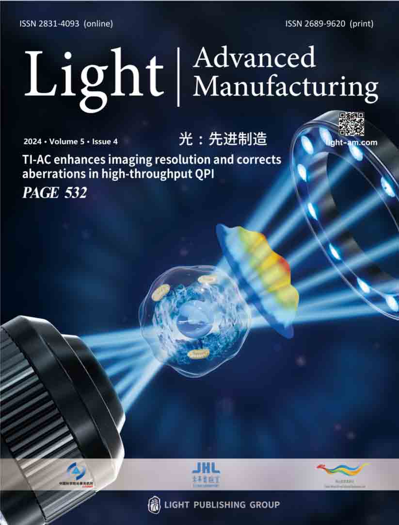
Photoluminescence spectroscopy is a powerful tool that helps to investigate the effectiveness of radiative recombination in semiconductors. It is also one of the most common methods used to study the influence of hard ionization on perovskite polycrystalline films. However, due to the general inhomogeneity of perovskite films prepared from the solution, single-point PL scans are not informative and can result in misleading conclusions. PL mapping is a more effective method to examine the defectiveness of the material as it shows PL intensity from the whole sample area. Fig.1a shows PL maps of fresh and exposed (6, 10, 21 kGy) polycrystalline perovskite films prepared on a glass substrate. The average intensity of the fresh and 6 kGy exposed samples is almost identical, which could be caused by the sample-to-sample variation. Further accumulation of dose results in noticeable PL enhancement. 21 kGy dose breaks the trend and brings PL values back and even below the initial values. Fig.1b represents the comparison of PL peak positions versus gamma- ray exposure. The peak intensity was averaged from the PL mapping data. It is clear that gamma-rays initiate phase segregation in the material, which was previously reported in a similar mixed halide system22. A fresh sample with PL peak @729 nm exhibits minor blue shift upon 6 kGy exposure and a pronounced shift upon 10 kGy exposure. Interestingly, the 21 kGy dose results in a reversible process, with PL peak shifting back to the 729 nm.
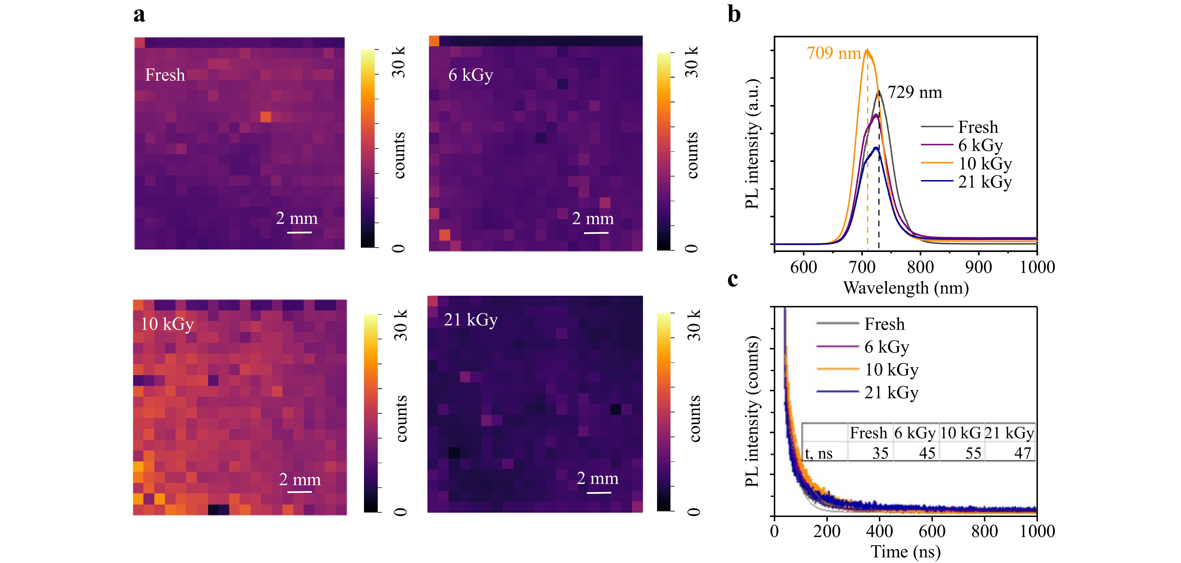
Fig. 1 Comparison of PL maps a and PL peak position b in gamma-ray exposed perovskite films. TRPL decay curves of fresh and exposed perovskite films c.
In this way, steady state PL spectroscopy revealed the gamma-ray threshold for Cs0.17FA0.83PbI1.8Br1.2 at 10 kGy where one can observe a pronounced enhancement of PL intensity and the biggest peak blueshift. Such results might point to some gamma-ray induced structural recrystallization that has a positive influence on radiative recombination and heals some of the defects in the material. More on the origin of the blueshift in exposed samples will be given in the discussion section.
Next, we performed time-resolved photoluminescence (TRPL) measurements to examine charge carrier lifetime evolution. The TRPL curve shows the time required for the excited carrier to recombine. Fig.1c shows decay curves following exponential behavior. There are different mathematical models used to fit TRPL decay curve, depending on type of the samples, excitation power density and other factors25,26. From mathematical point of view, biexponential model will fit better the experimental curve, however, in this case we will have two carrier lifetime components. Some reports use this model and calculate the average lifetime, which does not have physical meaning27,28. Even if we consider multiple recombination processes, TRPL curve still satisfies the single exponential trend25:
$$ {N\left(t\right)=Ae}^{-\frac{\left(t-t0\right)}{\mathrm{\tau }}}+c $$ (1) where: A – PL decay amplitude; t - Time of the decay, ns; τ – Carrier lifetime, ns; c – Constant characterizing diffuse light scattering background and electron noise background.
Table 1 summarizes the extracted parameters of the studied samples. It can be seen, that the carrier lifetime is the largest at 10 kGy dose and equals to 55 ns. Moderate doses up to 10 kGy initiate redistribution and partial passivation of defect states, which result in increase in carrier lifetime and recombination rate. TRPL dynamics over gamma ray dose has the same trend as in steady state PL – both analysis showed nonlinear behavior with the maximum at 10 kGy dose.
A τ c fresh 2149 35 17 6 kGy 1576 45 27 10 kGy 1581 55 15 21 kGy 1214 47 31 Table 1. Calculated parameters from TRPL decay curves.
The impact of gamma-rays on solar cells is more complex, and the role of interfaces becomes predominant. At the same time, we need to make sure, that there is no internal factors that could affect the experiment results. Fig 2S, ESI shows the comparison of EQE measured from the same sample after fabrication and after 6000 h of storage in glovebox. It can be seen that, the chosen configuration has a good internal stability and the contribution of internal factors in this experiment can be excluded. We prepared solar cells with the same perovskite composition and exposed them to gamma-rays. Fig. 2 shows the JV curve and solar cell structure before the exposure (a), EQE values (c) and maximum power point tracking curves of fresh and 21 kGy-exposed SCs (d). Fig. 3 shows the comparison of normalized short circuit current density (JSC), open circuit voltage (VOC), fill factor (FF) and power conversion efficiency (PCE) of fresh and exposed samples.
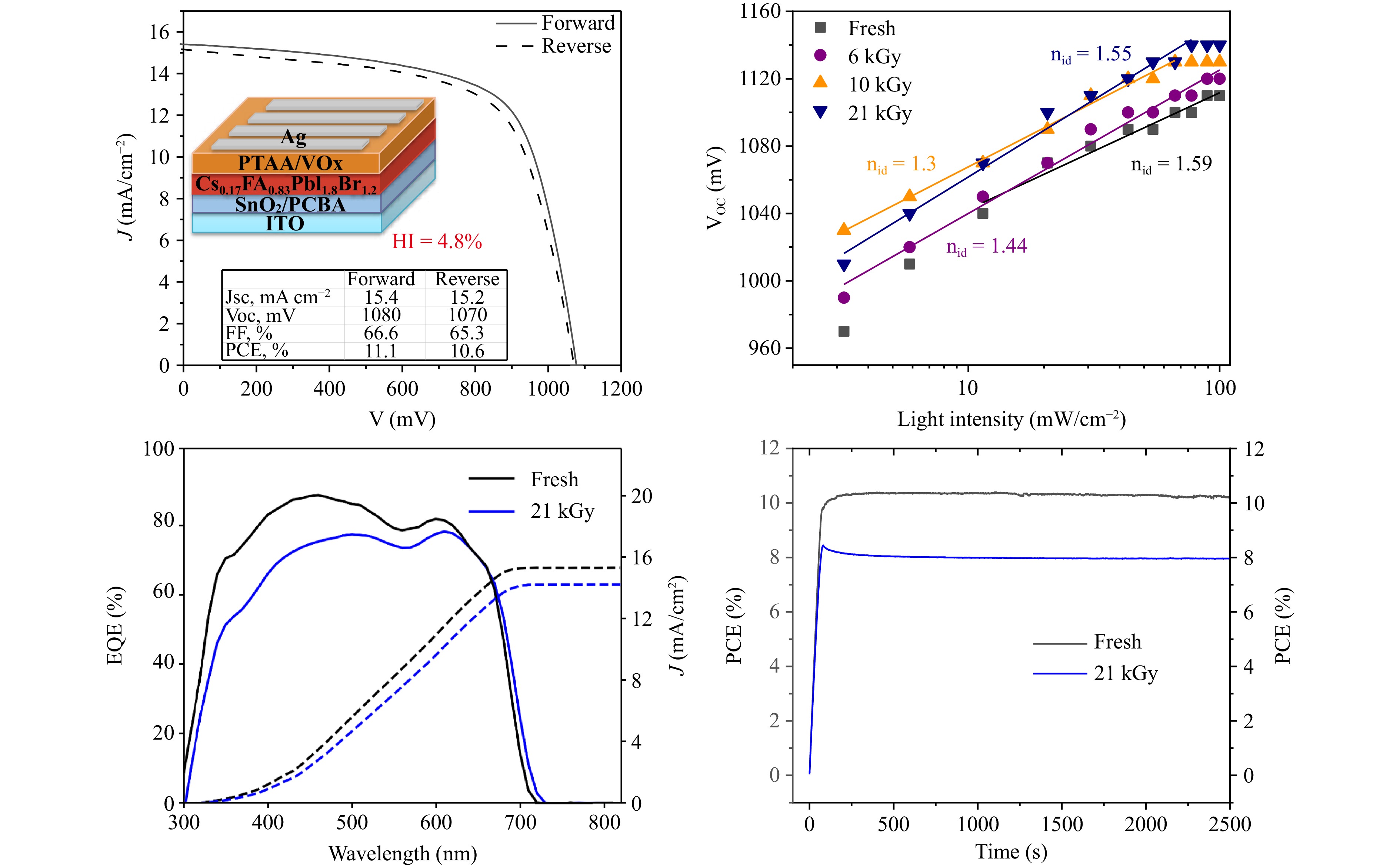
Fig. 2 The average JV-curve of the freshly prepared solar cells and its configuration a, Suns-VOC curves of fresh and exposed SCs with calculated ideality factors b, EQE of fresh and 21 kGy-exposed SC with integrated JSC c, Maximum power point tracking (MPPT) for fresh and 21 kGy-exposed SC.
Fig. 3 Comparison of solar cell characteristics before and after gamma-ray exposure.
The slow decrease in JSC is mainly caused by the substrate darkening, as earlier described in other works9. Glass transmittance decreases particularly in the 300−600 nm region29. Ionization generates free charge carriers that become trapped in vacancies or impurities. This creates color centers, which significantly reduce the optical transmission of glass and as a result – current density. VOC remained almost the same throughout all doses with 3−4% deviation, while FF decreased by 7% especially after 21 kGy dose. Some decrease in FF might point to the growing contribution of interface recombination, which lowers solar cell performance.
We additionally performed Suns-VOC measurements to see if there was any change in the recombination regime upon gamma irradiation. Fig. 2b shows a comparison of ideality factors nid before and after ionization. The ideality factor is a diode parameter that can tell about the recombination regime. It can be derived from the Shockley diode equation:
$$ {n}_{id}=\frac{q}{{k}_{b}T}\times \frac{dVoc}{dln\left({I}_{0}\right)} $$ (2) where: q – The absolute value of electron charge, 1.6 × 10⁻¹⁹ Coulombs; kb – Boltzmann constant, 1.38 × 10⁻²³ J/K; T – temperature, 298 K; VOC – Open circuit voltage, mV; I0 – Light intensity, mW/cm2.
Ideality factor usually lays between 1 and 2, with the following boundary conditions30:
nid = 1 e-h bimolecular radiative recombination regime;
nid = 2 trap assisted non-radiative recombination regime.
As one can see in Fig. 2b, nid of the fresh sample is 1.59, which is almost in between boundary conditions. First, nid decreases with dose going through the minimum at 10 kGy, which means that the recombination regime slightly shifts towards e-h bimolecular recombination. Further accumulation of dose causes reverse trend and nid increases to 1.55 that is shift towards trap assisted recombination regime. Suns-VOC plot presented in Fig. 2b is an auxiliary method that can help to observe some changes in recombination dynamics. However, it does not consider interface recombination, and some additional methods should be used to reveal it.
Electrochemical impedance spectroscopy (EIS) is an advanced method that can say more about interface recombination dynamics. Fig. 4 shows equivalent electronic circuits (a-b) and Nyquist plots (c), obtained during EIS measurements.
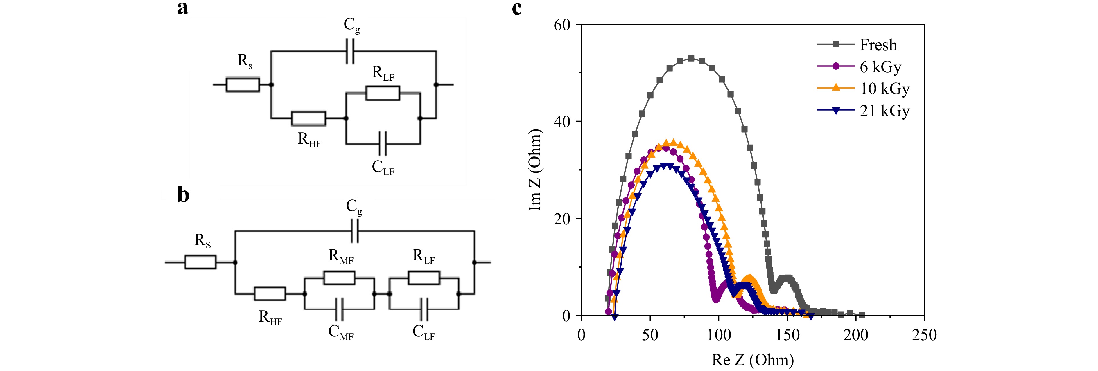
Fig. 4 Equivalent electronic circuits without middle frequency elements a and with it b. Nyquist plots for fresh and exposed solar cells under 1 Sun illumination (100 mW/cm2) and open-circuit conditions.
Here, we use a standard equivalent circuit consisting of two RC-elements (Fig. 4a) to fit the majority of spectra31. In this circuit, Rs stands for series resistance of electrodes and wires, Cg is geometric capacitance due to perovskite dielectric relaxation, which manifests at high frequencies, and RHF and RLF – resistances for high-frequency and low-frequency semicircles. It is generally quite difficult to discern their individual physical meaning. However, their sum equals to recombination resistance, Rrec = RHF + RLF. Finally, CLF is a capacitance stemming from the charge accumulation at the interfaces due to ionic movement and carrier trapping by surface defects. However, after irradiation with doses of 10 kGy and higher, an additional signature appears in the device impedance spectra. It manifests as semicircle at intermediate frequencies. We label the corresponding RC-circuit and mid-frequency (MF) and include it in the equivalent circuit (Fig. 4b). It is generally believed that such signatures arise due to insufficient carrier extraction rate at the interfaces with transport layers, which leads to additional charge accumulation32. The results of equivalent circuit fitting are listed in Table 2.
Parameter Fresh 6 kGy 10 kGy 21 kGy Rs, Ohm 23 23 28 29 Cg, F 1.7E-8 1.6E-8 1.3E-8 1.2E-8 RHF, Ohm 114 72 74 65 RLF, Ohm 27 24 23 21 RREC, Ohm 141 96 97 86 CLF, F 3E-4 5E-4 2E-4 3E-4 CMF, F − − 5.3E-7 9E-7 RMF, Ohm − − 9 14 Table 2. Equivalent circuit fitting parameters extracted from the EIS curves.
As can be seen from this table, the Rs and Cg values, expectedly, remain almost unchanged since those parameters are mostly affected by electrode quality, the perovskite thickness and its dielectric constant33. The decrease in RHF leads to a decrease in total Rrec. This means, that perovskite irradiation induces additional electroactive defects, most probably, in the bulk. Interestingly, RLF and CLF stay similarly unaffected by sample irradiation, which implies that device interfaces withstand radiation load fairly well and the interfacial trap density does not change significantly. However, the appearance of middle-frequency signature seemingly contradicts this. It can be speculated that such a behavior can be result of carrier trapping by interfacial shallow traps, which impede the carrier extraction but does not increase the non-radiative recombination rate much. Alternatively, this might be result of transport layer degradation.
All previous methods applied to solar cells can help to register changes in the recombination regime. In order to estimate the actual defect concentration and its variation with gamma-rays absorbed dose, we applied Admittance Spectroscopy (AS). Such measurements are particularly sensitive for device active layer properties and how it is affected by mobile ions. High concentrations of mobile charged defects can screen build-in fields on the Debye length scale resulting device structure capacitance to be:
$$ {C}_{\mathrm{i}\mathrm{o}\mathrm{n}}=\frac{\varepsilon\varepsilon_{0}A}{{L}_{D}} $$ (3) where: ε, ε0 – Dielectric constant of the perovskite and vacuum; A – Area, cm2; LD – Diffusion length, cm.
Diffusion length can be derived from the following equation:
$$ {L}_{D}=\sqrt{\varepsilon{\varepsilon}_{0}{k}_{B}T/\left({q}^{2}{N}_{i}\right)} $$ (4) where: kB – Boltzman constant, 1.38 × 10⁻²³ J/K; T – Temperature, K; q – The absolute value of electron charge, 1.6 × 10⁻¹⁹ Coulombs; Ni − Ion concentration, cm−3.
Fig. 5a, b show the evolution of capacitance and conductance of the solar cell before exposure, after 6 kGy and after 21 kGy accumulated dose. Here, at low temperatures, ions are fully immobile, and capacitance is determined by the geometric capacitance (Cg) of a structure. At high temperatures, all ions are quick enough to follow the applied bias of frequency ω. For a given diffusion coefficient D, the time it takes for a mobile ion to travel across $ {L}_{D} $ is$ {\tau =L}_{D}^{2}/D $. Therefore, the condition of being in the middle of the capacitance step from Cg to Cg + Cion of capacitance data C(T), or being at the peak of G/ω(T) data will be:
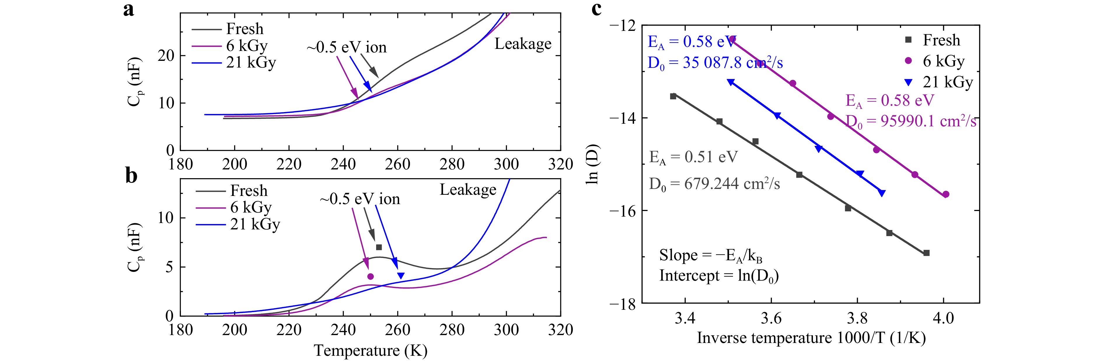
Fig. 5 a Step in the capacitance Cp and b peak in conductance G/ω of sample demonstrating potential screening due presence to ~0.5 eV mobile ion of exposed samples. c Arrhenius plot showing temperature dependence of diffusion coefficient obtained from AS measurements of sample at different doses.
$$ \omega \cdot \tau =1 \;\;\to \;\;\tau =\frac{\varepsilon{\varepsilon}_{0}{k}_{B}T}{{q}^{2}{N}_{i}{D}_{0}}\mathrm{e}\mathrm{x}\mathrm{p}\left(\frac{{E}_{A}}{{k}_{B}T}\right) $$ (5) and then activation energy EA and diffusion coefficient D0 of the registered defects can be determined from Arrhenius plot, presented in Fig. 5c.
AS results for sample with various absorbed doses, demonstrate the presence of a particular type of mobile ion with a diffusion activation energy EA of 0.51−0.58 eV and a diffusion coefficient D0 of 679−95990 cm2/s. Fig. 6 shows a combined plot of the registered defect’s concentration Ni and diffusion coefficient D0. It can be seen that D0 dramatically increases with 6 kGy dose achieving saturation at higher doses, while Ni on the opposite rapidly decreases. The origin of such unusual behavior will be discussed in the next section.
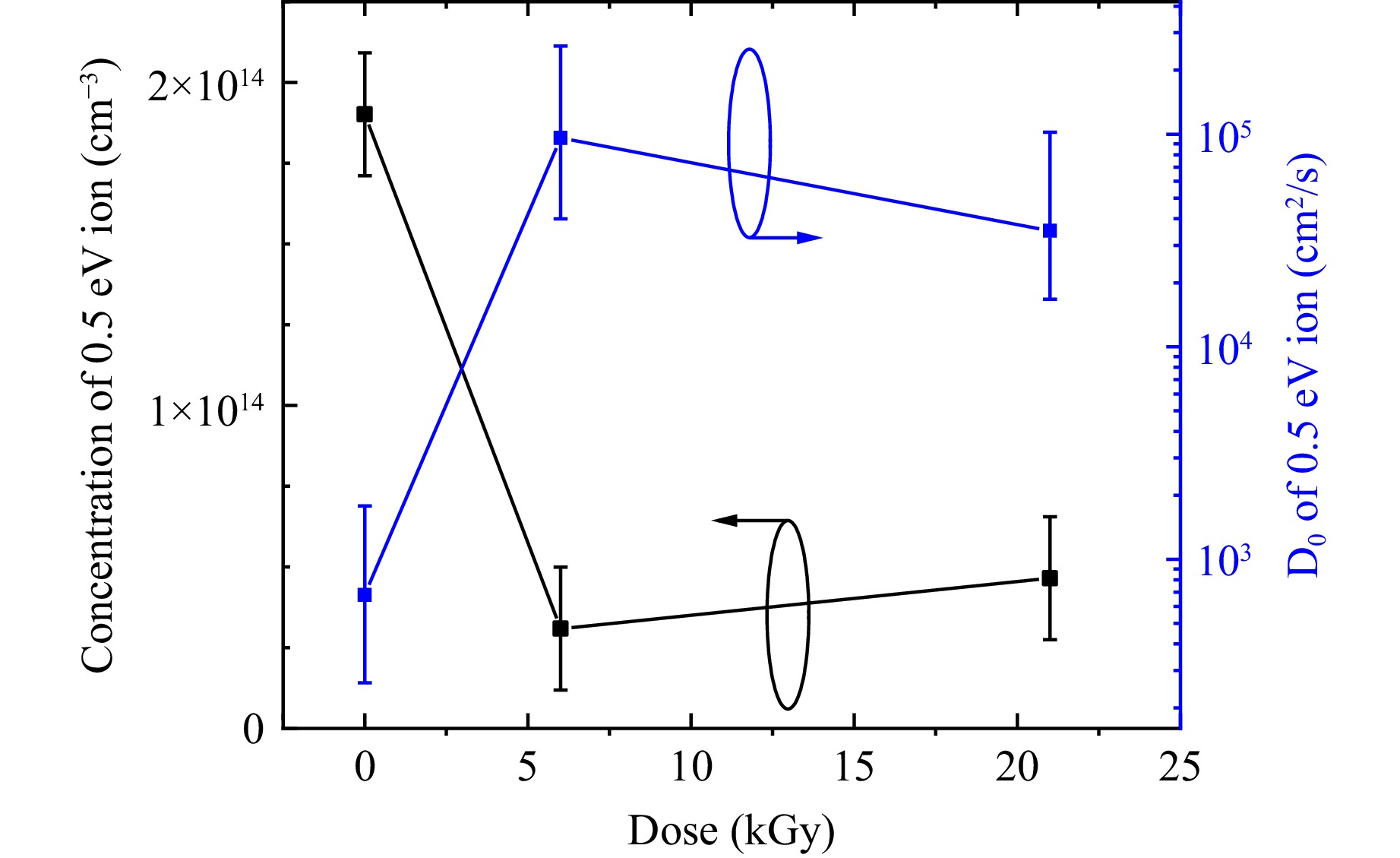
Fig. 6 Mobile ion concentration Ni (black) and Diffusion coefficient D0 (blue) as a function of absorbed dose.
The last but probably the most insightful analysis was performed on scanning transmission electron microscope (STEM). Fig. 7 shows high-angle annular dark-field scanning transmission electron microscopy (HAADF-STEM) images and energy-dispersive X-ray spectroscopy (EDX) maps of Pristine and Irradiated (10 kGy) solar cells. Interestingly, perovskite plane section of pristine sample has a large number of white spots, concentrated close to the interface with HTL. EDX maps revealed that it could be iodine ions. Moreover, pristine solar cell has less clear grain boundaries. After 10 kGy gamma irradiation we can see more pronounced perovskite grain boundaries and much less white spots corresponding to iodine ions. EDX map of the exposed sample shows that iodine moved away from the interfaces toward the bulk of the perovskite, making the iodine distribution more homogeneous along the plane.
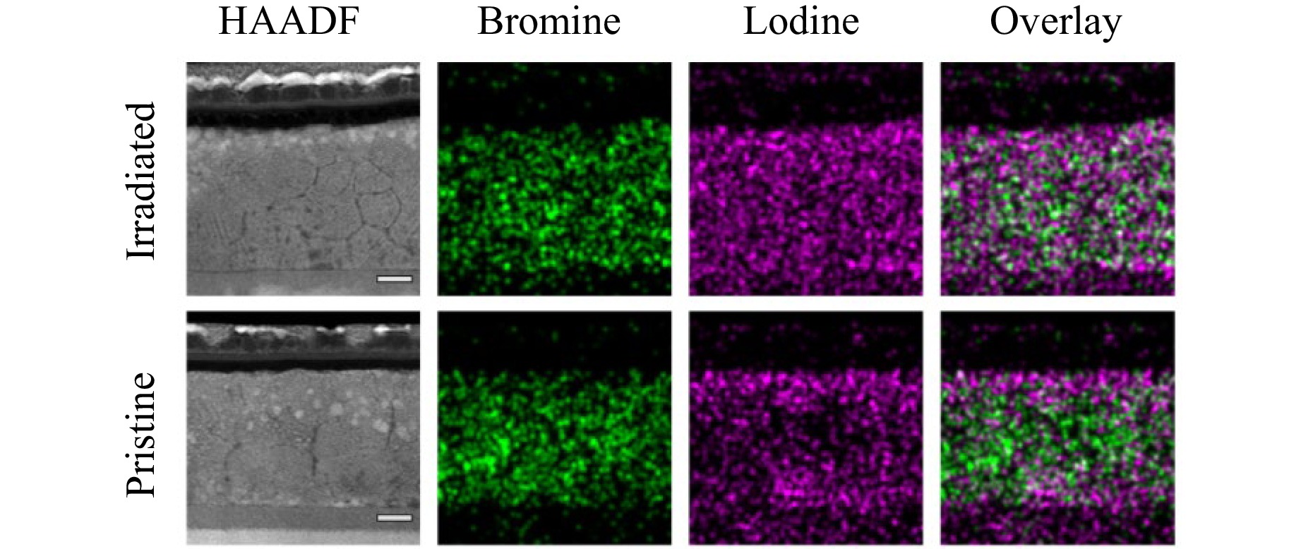
Fig. 7 High-angle annular dark-field scanning transmission electron microscopy (HAADF-STEM) images and energy-dispersive X-ray spectroscopy (EDX) maps of Pristine and Irradiated (10 kGy) solar cells. White marker correspond to 100 nm.
-
In this way, the applied several methods that showed a similar pattern both in thin films and solar cells. Bellow we will try to explain the mechanism that could be behind the observed trend.
When gamma-rays with photon energies of 662 keV interact with the matter, the probability of the photoelectric effect is higher than the formation of Frankel pairs. The photoelectric effect occurs when electrons, excited by gamma photons, escape from the matter, leaving behind unrecombined holes. Perovskite polycrystalline films typically have many interfacial defects, some of which are negatively charged. These negatively charged defect states, after interaction with gamma-rays, annihilate, reducing non-radiative recombination. While the fraction of negatively charged defects is high, we observe improvement in recombination dynamics and reduction of defect states. At some point, there is more newly formed defects after interaction with gamma-rays than a number of passivated defects. At such point, further accumulation of dose results in degradation of film quality and a shift towards non-radiative recombination. Similar behavior was recently observed in MAPbI3 films, but the gamma-ray threshold for this material occurred earlier, at around 3−5 kGy34. The key parameter that affects the mechanism of the interaction is the energy of gamma-ray source. More powerful gamma-ray sources with energies above 1 MeV could create more damage for perovskite films and solar cells. The probability of Frankel pairs’ formation would become higher. If the dose rate was higher, but the energy of gamma photons remained the same (662 keV) we would expect the same results but within shorter period of time.
An interesting phenomena was observed on PL spectra, presented in Fig 1b. Gamma-exposed films tend to blueshift with the strongest deviation after 10 kGy dose. 729 nm for the fresh sample corresponds to 1.7 eV bandgap which is slightly less than what should be for Cs0.17FA0.83PbI1.8Br1.2 perovskite. It could be due to the fact that laser in PL set up has the focus closer to the film surface, where we have accumulation of iodine as EDX presented in Fig. 8 showed. STEM analysis showed that gamma exposed samples have less iodine at the interface as it migrates to the bulk. Less iodine in the laser focus zone results in bandgap widening and PL blueshift. Interestingly, 709 nm Pl peak of 10 kGy exposed perovskite film corresponds to 1.75 eV bandgap which is the exact value for Cs0.17FA0.83PbI1.8Br1.2 perovskite. That also points on defect healing mechanism induced by gamma rays.
In solar cells, the process is more complex and can be interpreted differently. According to deep level transient spectroscopy (DLTS) and AS results reported previously35 defects that are common in perovskites with such compositions are formamidinium ion vacancies VFA as well as iodine vacancies VI. The observed decrease in the concentration of mobile ions may be due to their passivation or partial compensation by forming complexes with intrinsic defects induced by gamma-ray absorption. At the same time, an increase in diffusion coefficient points to migration through the freshly formed defects created by the gamma irradiation36. This probably means that the material has a number of inactive intrinsic defects that are activated by gamma photons, which result in such dramatic increase in D0 for the mobile ions with 0.5 eV energy. These results also imply a sophisticated combination of the mobile ion and its compensation and diffusion mechanisms, it behaves completely opposite as a Schottky-type defect should (when the diffusion coefficient increases with its own concentration)36. More evidence for iodine-related mechanisms of electric potential screening are brought from EDX mapping of pristine and irradiated sample’s cross-section (Fig. 7). Experimental results on this matter demonstrates higher relative concentration of iodine in near-contact region for pristine sample and more uniformly distributed iodine profile along current flow for irradiated sample. This correlates with both outcomes for 0.5 eV ion AS results. Concentration droop with absorbed dose (Fig. 6, black line) is detected in near-contact region by AS, and $ {D}_{0} $ rise by two orders (fig. 6, blue line) reflects possibility of more uniform mobile ion redistribution after irradiation.
Due to non-Schottky type of ion behavior the mechanism of mobile ion migration can-not be explained by simply assuming forming and interacting of only Ii and VI, thus the exact mechanism behind such complex behaviour still remains unclear and can be a topic for another research.
In summary, we made an attempt to analyse the impact of hard ionization (gamma-rays) on the wide bandgap perovskite films and solar cells. We were able to detect gamma- ray dose threshold at which most of the parameters reached saturation point. At 10 kGy dose perovskite thin films exhibit PL enhancement and increase in carrier lifetime, while solar cells exposed to 10 kGy dose have the lowest ideality factor. Admittance spectroscopy allowed to define the possible type of the defects (formamidinium or iodine vacancies) its concentration and diffusion coefficient. STEM microscopy confirmed the dominating role of iodine vacancies in the mechanism behind PSC gamma irradiation. It turned out, that small doses up to 10 kGy might passivate some of the negatively charged defects initially present in the perovskite films simultaneously activating other intrinsic defects. These two opposite processes result in impressive radiation tolerance of the studied wide bandgap perovskite up to 10 kGy dose. The impact of gamma-rays on solar cells is more complex and includes interface recombination, which was shown to grow at 21 kGy according to Impedance measurements. Defect concentration decreases with 6 kGy dose passing the saturation point somewhere between 6 and 21 kGy. All these results allow to conclude that Cs0.17FA0.83PbI1.8Br1.2 perovskite films and solar cells can resist doses up to 10 kGy which is more than enough for operation in space environment.
-
Glass substrates were cut in 2.5 cm2 pieces, manually cleaned with acetone and subjected to additional plasma cleaning for 300 sec. 106 mg of caesium iodide (CsI), 342 mg of formamidinium iodide (FAI), 443 mg of lead iodide (PbI2) and 528 mg of PbBr2 were dissolved in 2 mL of organic solvent (DMF) and stirred for 24 hours at room temperature for complete dissolving of all the components. 50 μL of the solution was deposited (dynamically) at 3000 rpm following by quenching with 100 μL of ethyl acetate (dropped 10 sec after perovskite precursor) applied at the same spin-coating frequency. The deposited Cs0.17FA0.83PbI1.8Br1.2 films were annealed for 10 min at 100 °C, which led to the development of a dark brown color.
-
ITO substrates (15 Ohm/sq Kintec) were cleaned by sonication in deionized water, acetone, and isopropyl alcohol (IPA) for 10 min each, dried in the air and subjected to a plasma cleaning (50 W, 300 sec). 10% suspension of SnO2 nanoparticles (Alfa Aesar) was deposited at 4000 rpm, followed by annealing on air at 170 °C for 20 min. Next, samples were introduced into a nitrogen glovebox for deposition of all remaining layers. PCBA [6,6]-phenyl-C61-butyric acid methyl ester was used as an effective passivator following the recipe described in other work37. Perovskite film was applied using the same method described earlier in the films preparation section. Solution of synthesized poly-triaryl amine PTAA (4 mg in chlorobenzene) was applied at 1000 rpm atop of perovskite layer. The detailed synthesis of PTAA is described in another manuscript38. The samples were left for drying within 10 min inside the glove box before loading into the vacuum chamber for deposition of the vanadium oxide and top electrodes. 30 nm of VOx was deposited atop PTAA layer on the whole sample surface. Silver electrodes (100 nm) were evaporated in high vacuum (10−6 mbar) through a shadow mask defining the active area of each device as ~0.16 cm2.
-
The gamma ionisator used in the experiment is a special set up with the cylindrical camera with 72 mm diameter. Gamma source covers 90 mm in height of this cylinder. Samples being placed inside the cylinder get the dose along the whole area. The prepared samples (thin films and solar cells) were packed in Al lamination foil inside the argon glove box. The set of samples consisted of 6 thin films and 6 solar cells which were exposed to 6, 10 and 21 kGy (2 samples per dose) with 137Cs gamma-ray source (E = 662 keV) with a dose rate of 2.5 Gy/min. Two reference samples for thin films and solar cells were left fresh inside glovebox for the same time as irradiated samples. After exposure to gamma-rays thin films were characterized with TRPL and PL within 2 hours. Solar cells were characterized with IV measurements.
-
The current-voltage characteristics of the devices were measured in nytrogen atmosphere using Advantest 6240A source-measurement unit under the simulated 100 mW/cm2 AM1.5G solar irradiation provided Wavelabs LS-2 AAA class solar simulator. The intensity of the illumination was adjusted using a reference silicon diode of a known spectral response. JV data was collected from 2 samples per each dose. Each sample consisted of 8 cells, with 16 JV measurements in total, where normally 3−4 cells were excluded from the statistics. JSC values were reconfirmed by integrating the external quantum efficiency (EQE) spectra against the standard AM1.5G spectrum. Ideality factor was calculated from Voc measurements performed at different light intensity from 1 to 100%.
-
Time-resolved PL measurements was performed in air atmosphere with TCSPC Time correlated single photon counter technique on Horiba QuantaMaster spectrofluorometer. Peak emission was set up to 710 nm, entrance slit 5 nm, time range 1.6 μs, 1000 counts for peak channel. Excitation power density – 2.54 nJ/cm2 and the excitation source – diDiode 345 nm. The excitation source was first going through the perovskite material and then through the substrate glass, that excludes the impact of gamma-ray-induced substrate darkening.
-
Photoluminescence spectra were obtained with Automatic Research GmbH LBIC+PL+EL microscopy setup with Horiba spectrometer. All samples were measured in air atmosphere from the perovskite side at 532 nm laser wavelength with 42 μW power, at 0.05 s integration time, 0.5 slit-width. PL maps were taken from 20х20 mm area of the samples with the following characteristics: 50 ms integration time, slit width 0.5 mm, step size-1 mm, integration diapason: from 690 to 730 nm. The maximum time each sample spent in air was ≈10 min. After the measurement the samples was taken back to the glovebox.
-
Impedance spectroscopy measurements carried out inside nydtrogen-filled glovebox using MFIA impedance analyser (Zürich Instruments). The spectra were recorded in the frequency range 1 Hz – 5 MHz under illumination intensity of 100 mW/cm2 at open-circuit DC bias and 10 mV AC perturbation. Data fitting was performed in Python using impedance.py package. For all measurements 0.08 cm2 shadow mask was used to define constant device area.
-
The Admittance Spectroscopy data was collected using the Keysight E4980A Precision LCR Meter over a frequency range of 20 Hz to 2 MHz. The measurements were performed in a liquid nitrogen cryostat manufactured by CryoTrade Engineering specifically LN120 model. This cryostat provided a low temperature environment for the sample being tested within 200÷320 K temperature range.
-
Samples for scanning transmission electron microscopy (STEM) were prepared using a focused ion beam (FIB) on a dual-beam scanning electron microscope from ThermoFisher, the Helios G4 Plasma FIB Uxe, operating with a xenon plasma. To minimize damaging effects, lamellae were cut and polished at an accelerating voltage of 8 kV throughout the entire process. After sample preparation, the FIB grid was immediately transferred to a transmission electron microscope, resulting in air exposure of the sample for less than one minute. High-angle annular dark-field scanning transmission electron microscopy (HAADF-STEM) images and energy-dispersive X-ray spectroscopy (EDX) maps were acquired using a ThermoFisher Titan Themis Z electron microscope operated at 200 kV, equipped with a Super-X system for energy-dispersive analysis.
-
This work was supported by Russian Science Foundation (project No. 23-72-01114).
Effect of gamma-rays on recombination dynamics and defect concentration in a wide bandgap perovskite
-
Aleksandra G. Boldyreva1, *, ,
 ,
, - Marina M. Tepliakova1,
- Artyom V. Novikov1,
- Vladimir G. Petrov2,
- Olga Parfenova1,
- Alexander A. Golubnichiy1,
- Anton Vasilev3,
- Danila Saranin3,
- Keith J. Stevenson2
- Light: Advanced Manufacturing 5, Article number: (2024)
- Received: 30 April 2024
- Revised: 03 September 2024
- Accepted: 17 September 2024 Published online: 19 December 2024
doi: https://doi.org/10.37188/lam.2024.053
Abstract: Herein, we have explored the recombination dynamics and defect concentration of a mixed cation mixed halide perovskite Cs0.17FA0.83PbI1.8Br1.2 with 1.75 eV bandgap after exposure to a gamma-ray source (2.5 Gy/min). We used photoluminescent spectroscopy to observe changes in recombination dynamics on perovskite films, impedance spectroscopy to reveal the contribution of interface recombination, and admittance spectroscopy to define the activation energy and concentration of defects. It was revealed that moderate doses (up to 10 kGy) passivate defects with activation energy ≈ 0.5 eV and at the same time form new defects that cause dramatic growth of the diffusion coefficient and migration of mobile ions. These two processes with opposite direction result in high radiation tolerance of the studied material and solar cells up to 10 kGy. Doses above 10 kGy are detrimental for perovskite solar cells, mainly due to the growing role of interface recombination. The results encourage the use of the wide bandgap perovskite Cs0.17FA0.83PbI1.8Br1.2 as a material for tandem solar cells with potential applications in a space environment.
Research Summary
Investigation of radiation hardness of perovskite solar cells for potential application in space
Perovskite solar cells may soon be implemented as a power source for satellites as recent publications revealed impressive stability towards ionizing radiation, including gamma photons. Impressive radiation hardness makes a group of semiconductors with perovskite structure an attractive candidate for multifunction solar cells. In this research, A. Boldyreva et al. focuses on Cs0.17FA0.83PbI1.8Br1.2 perovskite and discovers the gamma-ray threshold dose at which perovskite films and solar cells can be used without significant degradation in performance. The research group uncovers the mechanism of interaction between gamma-rays and solar cell components by using such advanced methods as time-resolved photoluminescence (TRPL), electrochemical impedance spectroscopy (EIS), Admittance Spectroscopy (AS) and Transmission Electron Microscopy (TEM) and finds an impressive correlation between the obtained parameters both in thin films and in solar cells.
Rights and permissions
Open Access This article is licensed under a Creative Commons Attribution 4.0 International License, which permits use, sharing, adaptation, distribution and reproduction in any medium or format, as long as you give appropriate credit to the original author(s) and the source, provide a link to the Creative Commons license, and indicate if changes were made. The images or other third party material in this article are included in the article′s Creative Commons license, unless indicated otherwise in a credit line to the material. If material is not included in the article′s Creative Commons license and your intended use is not permitted by statutory regulation or exceeds the permitted use, you will need to obtain permission directly from the copyright holder. To view a copy of this license, visit http://creativecommons.org/licenses/by/4.0/.

 DownLoad: