


-
Nowadays, perovskite photovoltaics is a technology that needs no introduction. Unprecedented rapid increase in efficiency from 3.8% up to 26.1% for single-junction solar cells in less than 15 years proved the bright future of the technology1,2. However, according to the recent market research, the most promising implementations can be achieved in the areas of indoor photovoltaics, semi-transparent devices and multi-junction solar cells3–5. Accordingly, the development of so-called wide bandgap (WBG) perovskite materials with Eg ≥ 1.7 eV becomes the key to the mentioned market areas. Significant progress was made in the field of WBG perovskite material design, where majority of the state-of-the-art WBG perovskite systems contain a mixture of ions6–9. The precise adjustment of the bandgap is achieved by altering the ratios of the both A cations and X anions in the ABX3 structure and such mixed-ion perovskites have superior performance and stabilized efficiency10. Some reports state that FA+ based WBG perovskites possess higher stability than MA+ based ones11. And introducing from y = 0.1 to y = 0.3 Cs+ increases the crystalline quality, carrier lifetime and mobility of FA1−yCsyPbIxBr3−x perovskites12.
But despite the significant progress in the chemical design of WBG perovskite materials, there are still some issues that need to be addressed. Photoinduced phase segregation often occurs upon illumination: halides separate into I-rich lower bandgap regions and Br-rich higher bandgap regions. The lower bandgap regions act as recombination centers for photogenerated charge carriers, causing voltage losses13. And Br-dominated inhomogeneities are formed in the perovskite structure, which leads to the poor film morphology with large amount of pinholes14. Grain boundaries and defects limit the mobility of the charge carriers and serve as recombination sites15. Overall, the defect concentration and phase homogeneity should be improved to enhance operational stability of the WBG perovskite material. Major strategies employed to achieve these goals include compositional engineering16,17, surface passivation18–20, solvent engineering21,22.
As we already mentioned, compositional engineering of WBG perovskites is highly developed topic. Same can be said about the passivation methods. There are approaches for directly address certain defects by certain passivators, as well as overall passivation for stability or device parameters improvement. And also the approach for the development of self-assembled monolayers. Unfortunately, there are not many publications dedicated to the solvent engineering method for WBG perovskites. Classic materials, namely, methylammonium lead iodide MAPbI3 were thoroughly investigated, and a number of successful methods including one- and two-step spin coating, antisolvent-free and solvent-free methods were developed23–25. Limited solubility of perovskite precursors in a single solvent leaded to the recommendation to apply mixed-solvent systems. Furthermore, the optimal ratio of additional DMSO solvent was found to be within the 20-40 vol. % range26. Also, a number of publications investigated the wet film formation processes for such materials as FAPbBr3, FAPbI3 and CsPbI327–29. Xu et al. implied NMP/DMF solvent system for MA0.05Cs0.12FA0.83Pb (I0.6Br0.4)3 perovskite and obtained higher efficiency relative to the DMSO/DMF solvent system30. Despite that, the solvent optimization for complex multi-cation and multi-anion materials is still in a nascent stage. Even for the materials with the same chemical formula, there can be several approaches for film deposition. For example, in various works, wide bandgap perovskite material Cs0.17FA0.83PbI1.8Br1.2 was deposited from pure DMF31, DMF:DMSO 9:132, DMF:DMSO 8:233, and pure DMSO solvents34, leading to the various device characteristics.
Here we present the first attempt to understand the influence of various binary solvents on the Cs0.17FA0.83PbI1.8Br1.2 wide bandgap perovskite film formation. We’ve chosen this MA-free based perovskite first introduced by McMeekin et al31. due to its optimal bandgap around 1.75 eV suitable for both indoor and multi-junction photovoltaics. In this work we implemented simple one-step spin-coating method with antisolvent application for its simplicity, reproducibility and the possibility to test various solvents in similar deposition conditions. During the investigation we considered traditional perovskite solvents N,N-dimethylformamide (DMF) and dimethyl sulfoxide (DMSO), also N-Methyl-2-pyrrolidone (NMP) and acetonitrile (AcN). It was demonstrated that implication of any binary DMF-X solvent improves the solar cell efficiency compared to the pure DMF solution. We also produced large area (25 cm2) modules with the best binary solvent combinations and demonstrated that despite the best efficiency in laboratory devices was achieved for DMF-DMSO processed solar cells, the best efficiency for modules was obtained for DMF-AcN devices.
-
For all of the following experiments we used a pure DMF solution of Cs0.17FA0.83PbI1.8Br1.2 with concentration of 1.2 M as a reference system. To investigate the influence of additional solvent we partially substituted DMF with either DMSO, NMP or AcN to keep the perovskite concentration constant, while concentration of additional solvent was set as 0 M (pure DMF references), 0.48 M, 0.72 M, 1.2 M, 2.4 M and for DMSO also 2.8 M. These values were chosen as corresponding to the total concentration of ions in solution: C(Br−) = 0.48 M, C(I−) = 0.72 M, C(Br−) + C(I−) = C(Pb2+) = 1.2 M, C(Br−) + C(I−) + C(Pb2+) = 2.4 M. Concentration of 2.8 M of DMSO is equal to 20 Vol%, which is one of the most often used ratios in DMF-DMSO binary solvent systems.
Fig. 1 demonstrates the n-i-p device architecture (ITO/SnO2/PCBA/perovskite/PTAA/VOx/Al) and influence of additional solvent concentration on its parameters: PCE, VOC, JSC and FF. Examples of J-V curves, EQE spectra and PCE statistics for the reference and best additional solvent concentrations can be found in Supplement (Fig. S1). Pure DMF reference system demonstrated efficiency around 11-12%, while partial substitution of solvent increased the efficiency up to 12-13.5% (2.4 M DMSO), 12-13% (0.72 M NMP) and 11.5-12.5% (1.2 M AcN). We can state that AcN addition mostly influenced the FF of the device, increasing it from 60% to 67%. NMP addition increased device JSC from 17.3 up to 18.3 mA/cm2. And DMSO influenced both JSC (from 17.3 up to 18.5 mA/cm2) and FF (from 60 up to 67%), leading to the highest increase in PCE. This implicates the different reasons behind the solvents influence on device performance. To determine these reasons further investigations were performed mostly for four solvent compositions: pure DMF as reference, AcN 1.2 M, NMP 0.72 M and DMSO 2.4 M as the best representatives for each binary combination.
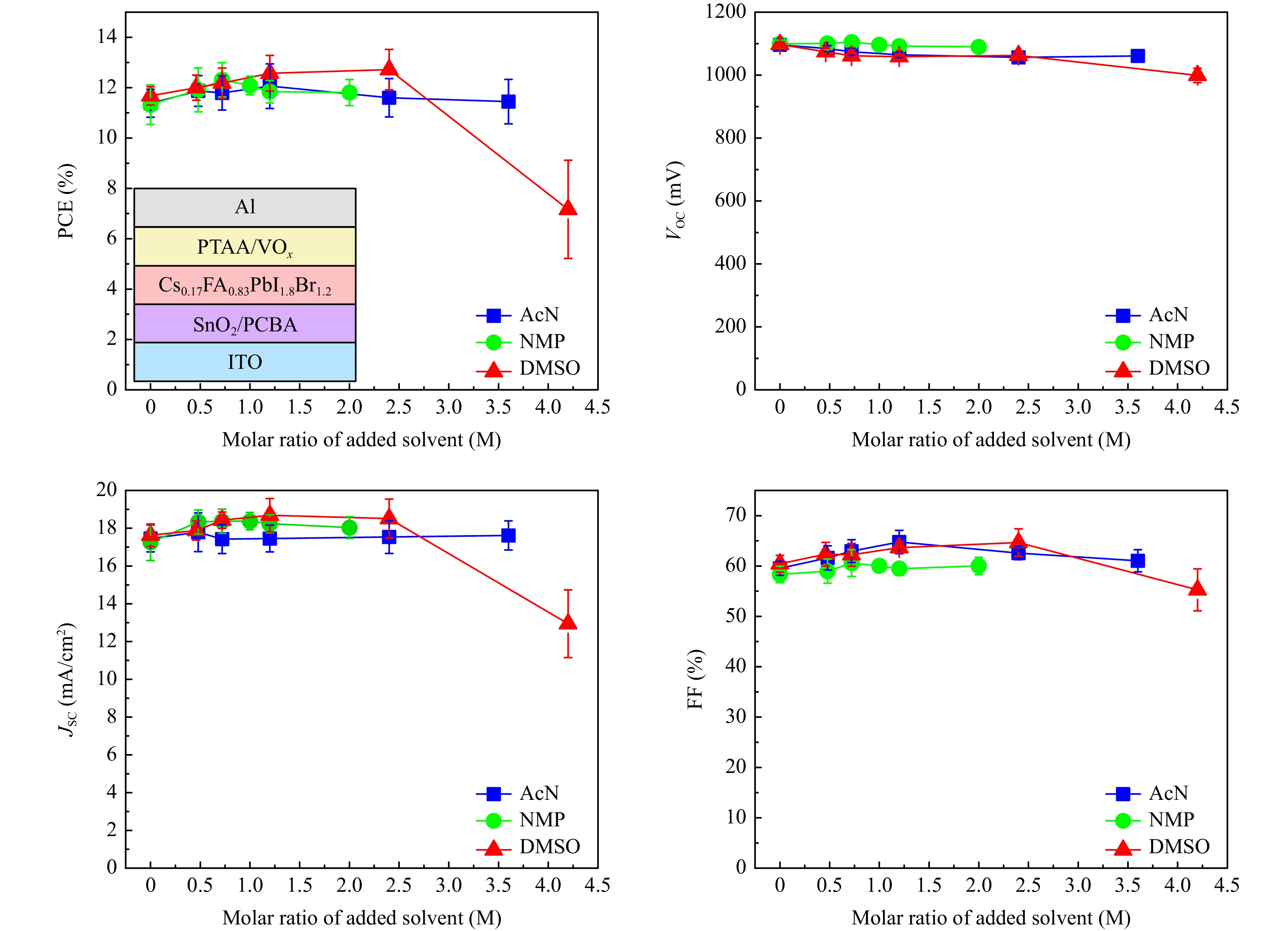
Fig. 1 Influence of DMF solvent partial substitution with AcN, NMP or DMSO on solar cell parameters. Here presented all main solar cell parameters PCE, VOC, JSC and FF. Inside the PCE figure, the device architecture for this test is presented.
UV-Vis spectra (Fig. 2a) demonstrated slight increase of intensity for AcN 1.2 M and NMP 0.72 M perovskite films deposited on glass substrate compared to the pure DMF, while DMSO films demonstrated the highest absorption. This effect is most likely related to the increase in thickness of DMF-DMSO film, which is expected because DMSO has highest viscosity and boiling point among all presented solvents. The broad wave in the near-IR on absorption spectra is related to the interference of light reflected from both sides of the perovskite layer. SSPL from the same samples revealed that only DMSO addition increased the PL intensity (Fig. 2b). Time-resolved photoluminescence (TRPL) was used to determine the relative defect density in different samples, because the decrease in charge carrier lifetimes is reflected in a fast PL decay35. In Supplement (Fig. S2) the TRPL profiles with different solvents are presented. The shape of the TRPL profiles depends on the rate of competitive recombination processes: fast trap-assisted recombination (non-radiative) and slow bimolecular recombination (radiative)36,37. Therefore, the TRPL profiles for perovskite materials are usually fitted with exponential decay function:
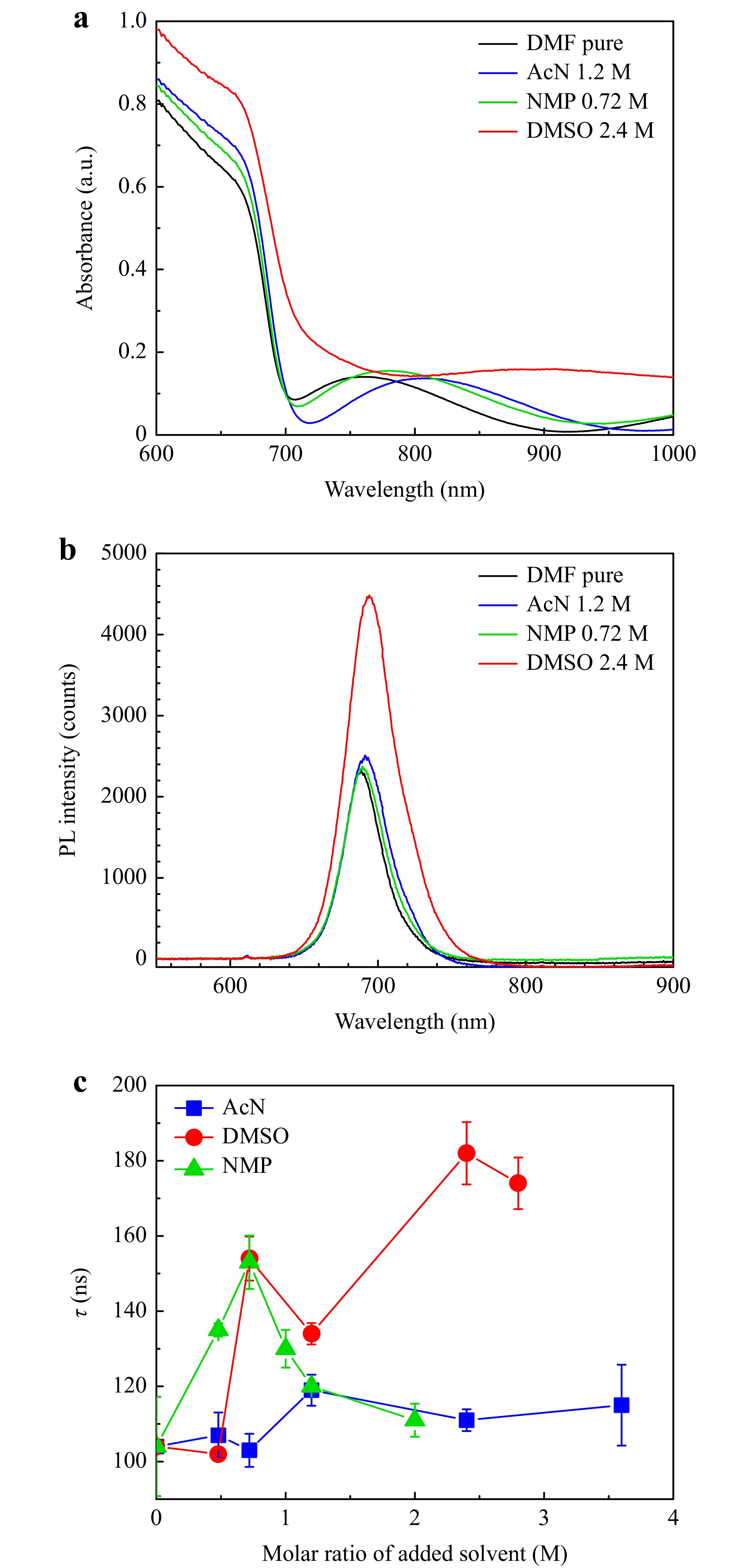
Fig. 2 UV-Vis a and PL b spectra of perovskite films on glass substrates processed from different solution compositions. Influence of additional solvent concentration on the average lifetime of charge carriers τ calculated from the TRPL data c.
$$ N\left(t\right)=A{e}^{\frac{-t}{\tau }} + C $$ where $ A $ is PL decay amplitude, $ t $ is the decay time, τ – time of average recombination decay, C is a constant characterizing electron noise and diffuse light scattering background. Dependence of the average charge carrier lifetimes from the additional solvent concentration is shown in Fig. 2c. Average charge carrier lifetimes increase with any solvent addition. It is also noticeable that the shape of τ dependency resembles that of PCE dependency on additional solvents molar concentration: peak at 1.2 M for AcN, at 0.75 M for NMP and at 2.4 M for DMSO. Therefore, it is possible that improvement of device performance is related to the decreased defect density in WBG perovskite.
The most significant changes in device basic parameters were observed in XRD spectra (Fig. 3a), where intensity increased for both AcN 1.2 M and NMP 0.72 M, while addition of DMSO inverted the intensity of peaks, making 20.3° and 32.3° dominant. This fact leads to the assumption that addition of NMP and AcN increases the grain size in perovskite film, while DMSO additionally changes the occupancy of crystallographic positions. The whole effect of XRD change depending on additional solvent concentration can be observed in Supplement (Fig. S3).
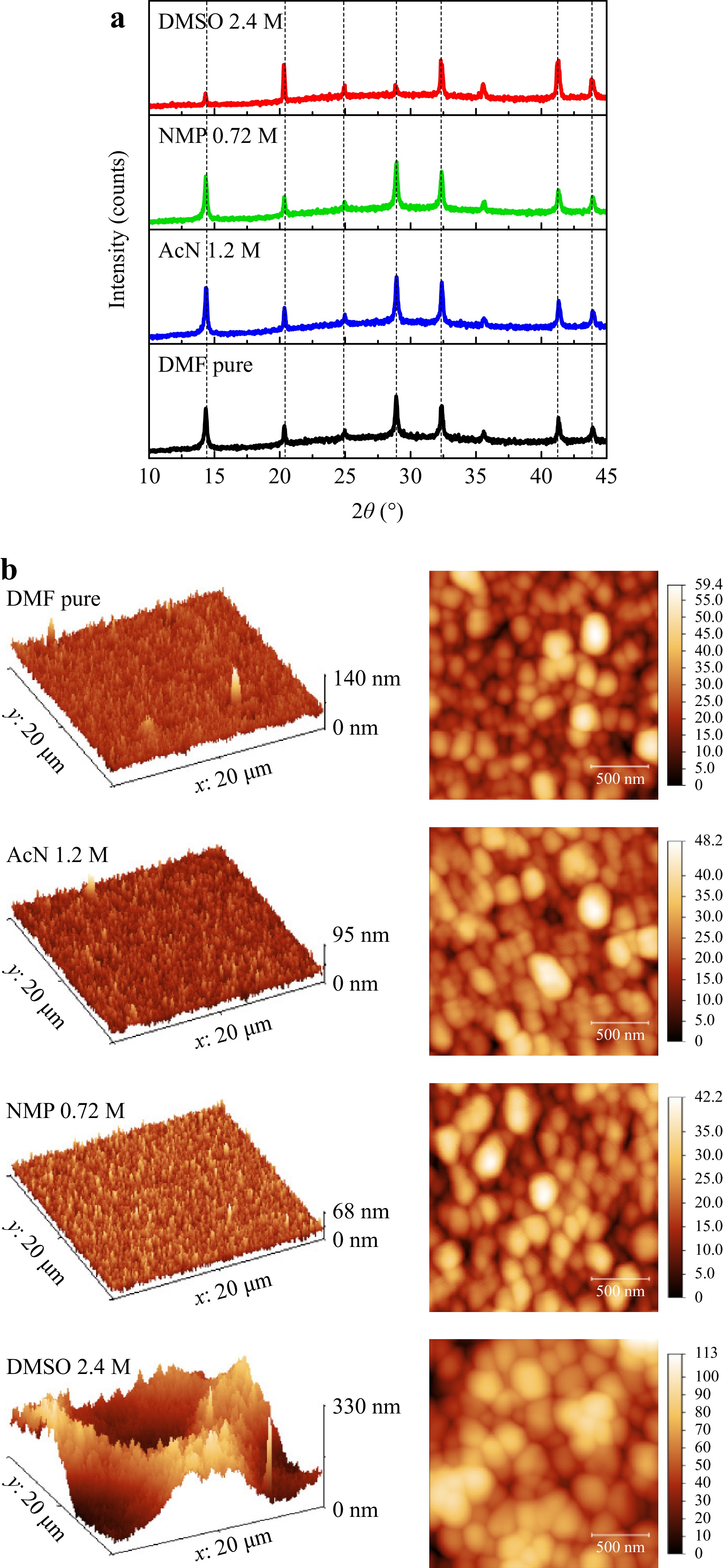
Fig. 3 XRD spectra for perovskite films on glass substrates processed from different solution compositions a. 3D AFM profiles for 20x20 µm scan area and 2D AFM profiles for 2x2 µm scan areas, perovskite films on glass substrates processed from different solution compositions b.
AFM data confirmed the assumption of grain size growth (Fig. 3b), but we additionally performed SEM measurements from the film surface (Supplement Fig. S4). AFM also revealed the improvements in perovskite film quality, as numerous defects visible for flat DMF films disappear for AcN 1.2 M and NMP 0.72 M films. The surface of the perovskite films with AcN addition remains flat up to 3.6 M of AcN added (Supplement Fig. S5). But only 1.2 M AcN samples demonstrated the grain size growth compared to the reference. Similar effect was observed for NMP addition up to 0.72 M. Further addition of NMP leaded to the formation of grain clusters (Supplement Fig. S5), which probably caused the further observed increase of XRD intensity, but decreased the average charge carrier lifetime and device PCE.
With the DMSO introduction, films surface becomes more and more uneven, forming hills and valleys and becoming “wrinkled” (Fig. 3b, Supplement Fig. S5). Increase of DMSO concentration makes “wrinkles” larger and deeper. Wrinkled morphology is typical for mixed ion perovskites, and it appears due to relaxation of internal stresses during crystallization caused by misfits in ion sizes (e.g. the size of Br− and I− is 1.96 and 2.22 Å, respectively)14. Wrinkles and folds in the surface effectively localize and trap light, which greatly improves light harvesting capabilities in optoelectronics38. Same effect is implemented in traditional structured silicon wafers for effective light harvesting in solar cells. That means that high JSC for DMSO devices may be additionally attributed to their morphology. Simultaneously, “wrinkles” influence the film absorbance, as the light trapping increases the interference, leading to the lift in the UV-Vis baseline.
AFM method also allowed us to check the assumption of increasing of the film thickness, related to the additional solvents. Thickness of pure DMF films was confirmed at 350 ± 10 nm. Addition of 1.2 M AcN or 0.72 M NMP did not lead to changes in the film thickness. However, DMSO 2.4 M films demonstrated the variation of thickness parameters because of “wrinkled” morphology from 300 nm up to 390 nm.
To get a deep insight into the influence of solvents on defect state in complete devices, we performed a series of investigations: Suns-VOC, SCLC and Impedance spectroscopy (Fig. 4a-d). Impedance spectroscopy and Suns-VOC were measured from the mentioned earlier device architecture ITO/SnO2/PCBA/perovskite/PTAA/VOx/Al, while for SCLC measurement we used electron-only configuration ITO/SnO2/PCBA/perovskite/PCBM/BCP/Mg/Al, where PCBM is Phenyl-C61-butyric acid methyl ester and BCP is bathocuproine. We would like to note that SCLC is not a directly precise method for trap concentration measurement. There definitely might be a number of measurement errors related to the sample-to-sample variation or imprecisely measured film thickness, especially given that perovskite films are not completely smooth, so some natural thickness variation is always present. In our case we did our best to eliminate these errors by measuring perovskite’s thickness at least 5 times for each perovskite and taking the average value. Similarly, we have measured several SCLC devices for each system. Another major source of errors is the presence of Schottky barriers or other contact non-idealities in the device. They will significantly affect the I-V curve distorting the measured results. For this reason, we have used Mg layer with very low work function as injection electrode in the electron-only devices. Magnesium’s low work function ensures Ohmic contact with n-type semiconductor. Additionally, for halide perovskites, ionic conductivity can play its role in the overall shape of the curve. We have employed pulsed SCLC measurements to minimize the impact of the ionic conductivity.
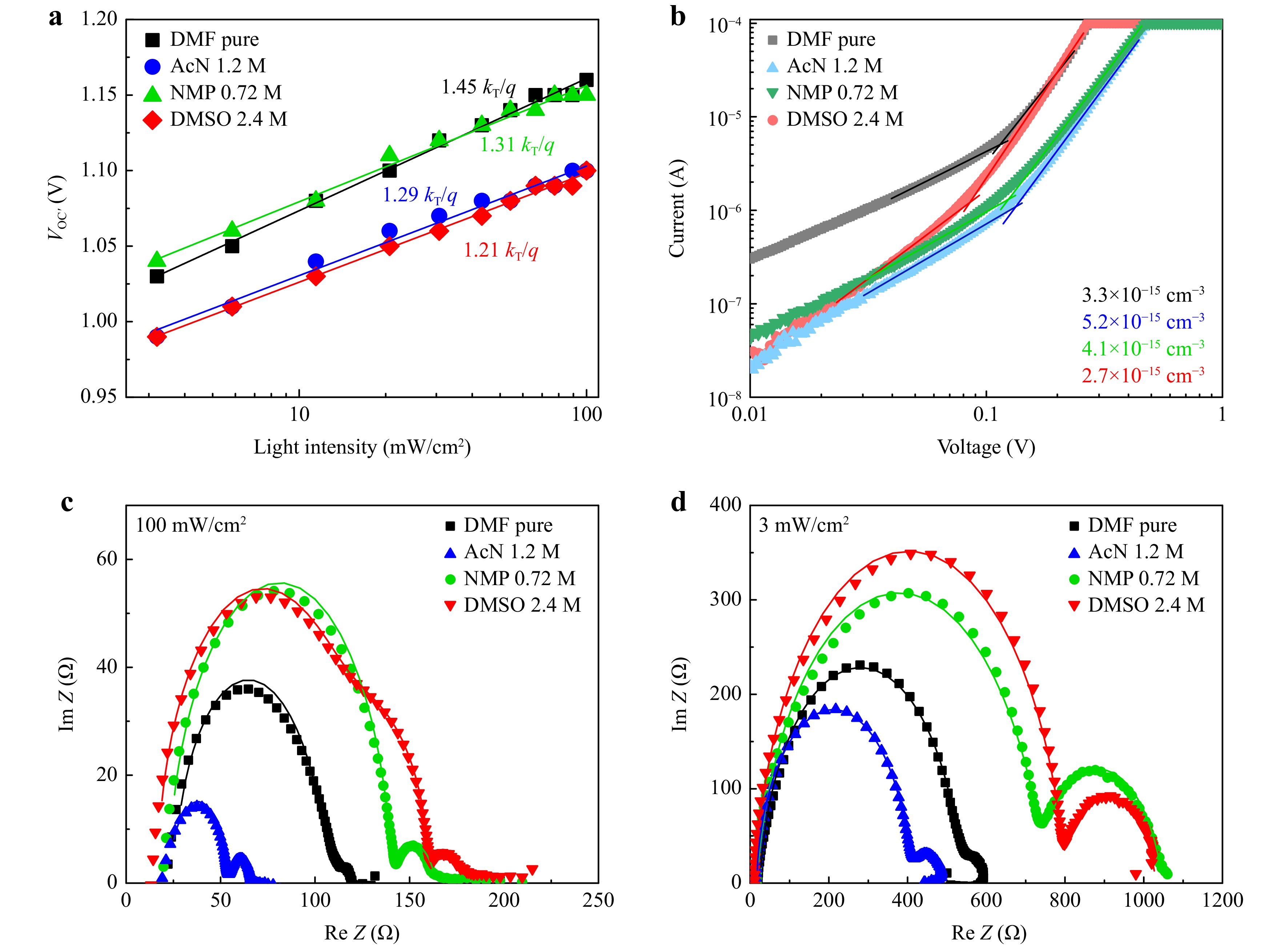
Fig. 4 Suns-VOC data for ITO/SnO2/PCBA/perovskite/PTAA/VOx/Al n-i-p solar cells based on four solvent compositions for perovskite layer a. SCLC curves for electron-only devices ITO/SnO2/PCBA/perovskite/PCBM/BCP/Mg/Al based on four solvent compositions for perovskite layer with calculated concentration of electron traps b. Impedance spectroscopy curves for ITO/SnO2/PCBA/perovskite/PTAA/VOx/Al n-i-p solar cells based on four solvent compositions for perovskite layer measured at 100 mW/cm2 c and 3 mW/cm2 d.
Suns-VOC allowed us to calculate the ideality factor for each solution composition and demonstrated the highest ideality factor for pure DMF devices 1.45. AcN 1.2 M demonstrated ideality factor 1.29, NMP 0.72 M – similar 1.31 and DMSO 2.4 M – the lowest 1.21. SCLC revealed the values of electron trap density. DMSO 2.4 M demonstrated the lowest concentration of electron traps, which correlates well with the lowest ideality factor value.
Impedance spectroscopy (IS) was measured at two light intensities 100 mW/cm2 (Fig. 4c) and 3 mW/cm2 (Fig. 4d). We also measured dark IS before and after the JV measurement of the devices, the results are present in Supplement Fig. S6. Equivalent circuits used for curve fitting were taken from the Ref. 39 and are presented in Supplement Fig. S7. Calculated parameters are presented in Supplement Table 1-2. NMP 0.72 M and DMSO 2.4 M consistently show high recombination resistance at both light intensities. This means that their recombination rate is lower than in pure DMF and AcN 1.2 M devices. Interfacial trapping-related low-frequency capacitances CLF are comparable in most cases: under 100 mW/cm2 difference is negligible, while under 3 mW/cm2 AcN has the highest CLF, which correlates well with the highest trap density in SCLC. DMSO has mid-frequency semicircle at 100 mW/cm2, definitely absent from all other systems and low-light DMSO spectrum. It means that at high carrier density transport layers extract charges slower than they are generated. For the dark IS measurement (Supplement, Fig. S6, Table 2) DMF and DMF:NMP-based samples show little change in parameters after the JV measurements. For DMF:NMP a small improvement can be seen by the increase of recombination resistance and decrease of charge transfer resistance. In contrast, DMF:DMSO and DMF:AcN systems feature notable drops in RLF values which might point at slight increase in the interfacial trap density after light exposure. This is likely due to mobile ions that disrupt the interface under illumination. However, one should also note that these changes are still fairly small – about 10%.
Cross-sectional scanning electron microscopy was performed to obtain the images of the representative device cross-sections (Fig. 5). The pure DMF perovskite layer contains numerous inhomogeneities, which mostly disappear after the solvent modification. AcN 1.2 M film quality changes the most significantly: smooth surface, best among all the materials, constant non-defect thickness, grain boundaries become slightly visible. Similar effect was observed for NMP 0.72 M, but some intrinsic defects are still present in the perovskite film, especially on grain boundaries. DMSO 2.4 M perovskite film is homogeneous with clearly visible grain boundaries. It’s also noticeable that the thickness of all bisolvent systems is higher than for pure DMF film, and DMSO 2.4 M film has the highest, but not constant thickness.
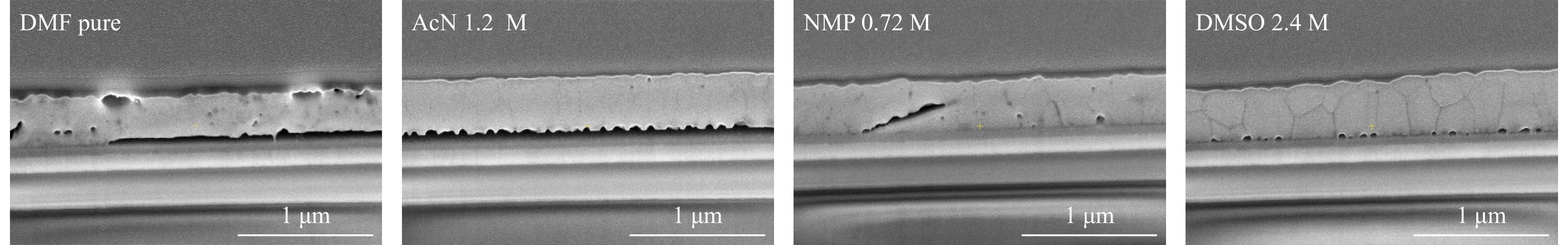
Fig. 5 Cross-sectional SEM for ITO/SnO2/PCBA/perovskite/PTAA/VOx/Al n-i-p solar cells based on four solvent compositions for perovskite layer.
To understand the influence of additional solvents on perovskite material and device photostability, we proceeded with express test in inert atmosphere and simulated sunlight of 100 mW/cm2 for solar cells and thin films on glass substrates covered with PTAA and VOx layers. We observed the dynamics in film absorption (Fig. 6a) and normalized device PCE (Fig. 6b). Dynamics for all film UV-Vis spectra and solar cell parameters is presented in Supplement Fig. S8-S12.
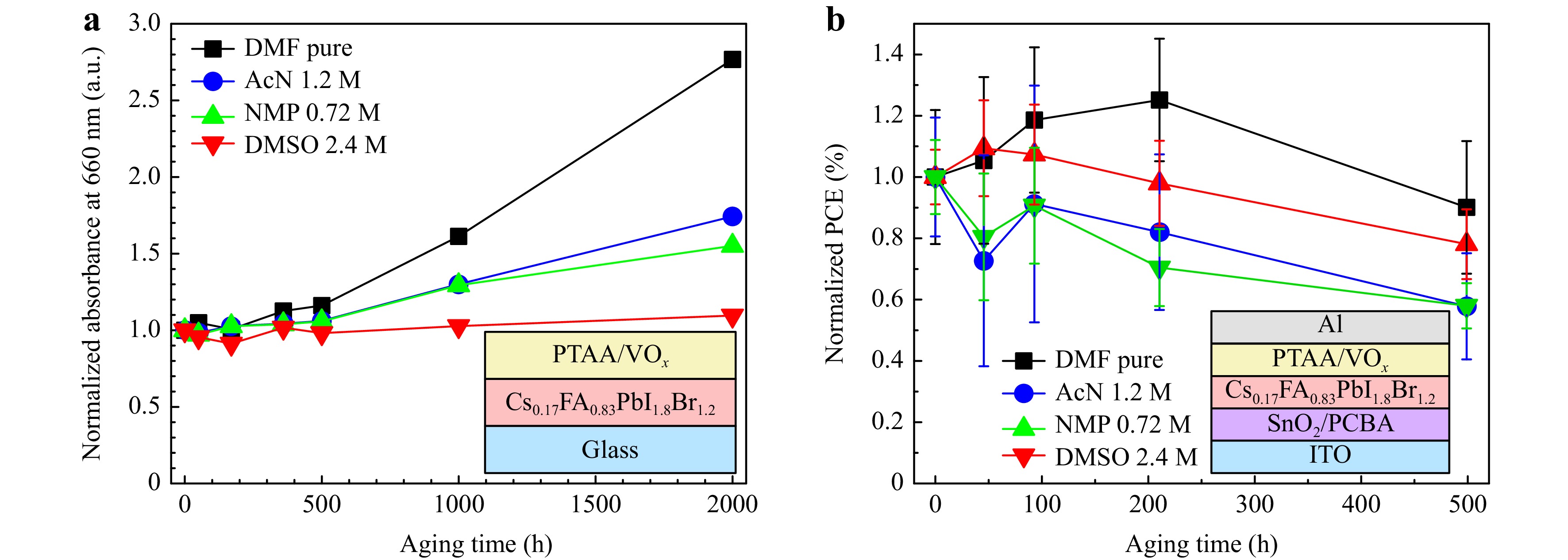
Fig. 6 Normalized dynamics in UV-Vis spectra change at the wavelength 660 nm depending from the used additional solvent a. Normalized dynamics in solar cell PCE change depending from the used additional solvent a. Degradation conditions were 100 mW/cm2 light intensity in inert conditions. Full UV-Vis spectra for all solvent concentrations can be found in Supplement Fig. S8-S11. Full un-normalized data for all device parameters can be found in Supplement Fig. S12.
-
We identified the positive influence of all three used co-solvents AcN, NMP and DMSO on device parameters. It was noticeable, that all three solvents have various reasons behind the efficiency growth. Additional experiments conducted on perovskite thin films and full devices provided us with information necessary to make the following conclusions and assumptions.
Addition of 2.4 M DMSO (17.2 Vol%) leaded to the simultaneous increase in JSC and FF (Fig. 1). Significant growth of current is mostly related to the “wrinkled” morphology and grain size growth, visible by SEM (Supplement, Fig. S3), Cross-sectional SEM (Fig. 5) and AFM (Fig. 3b). Improved quality and size of grains also leaded to the FF improvement. Increase in SSPL spectra indicates the growth in free charge carrier concentration. However, introduction of DMSO solvent leads to the strengthened interface recombination and appearance of injection barriers from the perovskite layer to the charge-transport layers. This can be confirmed by the slight decrease in device VOC with DMSO addition and appearance of third semicircle on the impedance spectra measured at 100 mW/cm2 as well as decrease of RLF and increase of CLF calculated from impedance spectroscopy (Supplement Table 1-2). We can also assume that the ideality factor of 1.21 which is closest to 1 among all solvents, in combination with low VOC value indicates the dominance of interfacial Shockley-Read-Hall recombination35. This could happen due to the film morphology, since the following hole transport layer PTAA was deposited via spin-coating method, and resulting PTAA film quality and perovskite/PTAA interface can be disrupted by non-uniform deposition surface. It can also be partially related to the worsened adhesion of perovskite solution to the electron-transport layer, which was checked with contact angle technique (Supplement Fig. S13) with observed increase in contact angle value.
0.72 M on NMP (7 Vol%) enhanced the JSC of the perovskite solar cells and very slightly increased the FF with almost no effect on VOC. Usually the perovskite film thickness is the one responsible for the current density increase, but not in this particular case, since nor Cross-sectional-SEM, nor AFM, nor UV-Vis indicated any changes in perovskite thickness. Increase of charge carriers lifetime (Fig. 2c) and lower ideality factor (Fig. 4a) implied the slight improvement of perovskite film bulk quality, but cross-sectional SEM still demonstrated the presence of defects, mostly concentrated between the perovskite grains. And almost no changes in CLF and RLF calculated from impedance spectroscopy indicated that addition of NMP does not deprave the interface between the perovskite and CTLs, unlike the addition of DMSO and AcN.
1.2 M concentration of AcN corresponding to the 8.6 Vol% leaded to the noticeable growth of solar cell FF from 60% to 67%. The FF of the solar cell mostly depends on the charge transport in all functional layers and charge extraction from perovskite into charge transport layers40. However, according to the device investigation by impedance spectroscopy and SCLC measurement (Fig. 4), the recombination rate and trap density for DMF:AcN devices only increases. So the main reason behind the improved FF and PCE of the device is drastically improved bulk film quality observed by AFM (Fig. 3b) and cross-sectional SEM (Fig. 5), which also affects the charge transport in the perovskite layer because of reduced series resistance. This effect was proved by TRPL conducted for perovskite films (Fig. 2c) and ideality factor (Fig. 4a). The problem still lays within the interface between the perovskite and CTLs. Since the morphology of the film was the best among the four and the adhesion of AcN 1.2 M perovskite solution was the best among all compositions according to the contact angle (Supplement Fig. S13) we can make a hypothesis that some carrier traps can accumulate on the interface between the perovskite and CTLs. The nature of this traps should be investigated by more advanced methods and there is a high possibility that a direct passivation approach could further improve the DMF-AcN processed perovskite material.
There are obvious solvent properties that always influence the film formation process strongly, such as density (DMF - 0.94 g/cm3, AcN - 0.79 g/cm3, NMP 1.03 g/cm3, DMSO - 1.1 g/cm3) and dynamic viscosity (DMF - 0.92 mPa·s, AcN - 0.35 mPa·s, NMP 1.65 mPa·s, DMSO - 1.996 mPa·s). High dynamic viscosity of DMSO might be the reason behind the worsened adhesion of DMF:DMSO solution to the ETL, but simultaneously it influences the grain formation and, as expected, their size and film morphology. But this won’t be the same for AcN solvent, which has lower density and viscosity than DMF. Another important parameter is boiling temperature of the solvent (DMF - 153°C, AcN - 82°C, NMP - 202°C, DMSO - 189°C). Slower evaporation of high boiling point solvents like DMSO and NMP might induce slower crystallization which favors the growth of larger grains. Indeed, our AFM data supports this assumption (Supplement Table 4). After the solution deposition and antisolvent application we heat up samples to ensure the grain growth and evaporation of the remaining solvents. And since we heat up our films up to 100-120°C, then there is high probability, that some amount of DMF, DMSO and NMP molecules will remain in the perovskite film. The influence of the remaining solvent molecules can be both positive, if they are concentrated on grain boundaries providing surface trap passivation, or negative, if they are concentrated in the bulk where they can produce impurity states within the bandgap. And the probability for AcN molecules to remain in the film will be much lower because of its low boiling temperature. Finally, all our solvents have a dipole moment (DMF - 3.82, AcN - 3.92, NMP - 4.09, DMSO 3.96), which influences the lead coordination in the mixture solution, the higher the dipole moment — higher the coordination capacity of a solvent. However, the values of dipole moments are fairly close, therefore, we don’t expect any considerable influence from this factor.
Photoinduced degradation of perovskite films covered with PTAA/VOx revealed the positive effect of binary solvents on stability, which is unsurprising since all three additional solvents improved the bulk perovskite film (Fig. 6). The best stability was observed for DMSO 2.4 M films. Overall, all systems demonstrated rapid degradation of films, which is most likely related to the phase segregation. On some of UV-Vis spectra the formation of a perovskite shoulder close to 800 nm can be observed, which corresponds to the formation of the new phase (Supplement Fig. S9-11). Surprisingly, when we switched to the device photoinduced degradation, the most stable solar cells were ones with pure DMF based perovskite. However, this effect is deceptive, since the efficiency increases in the beginning of the process for pure DMF system, which is also related to the phase segregation and formation of narrow-bandgap phase. Binary solvent systems did not demonstrate such increase in efficiency from the start. But still, the degradation of all perovskite solar cells is most likely related to the phase segregation. We also would like to point out the necessity to improve the interfaces of perovskite/CTLs according to our previous assumptions that addition of both DMSO and AcN in perovskite solution negatively influences the interface quality in solar cell, while improving the bulk. The development of the suitable CTLs for WBG perovskite materials is necessary to ensure their stability and improve device parameters, since the SnO2 and PTAA energy levels align well with MAPbI3 and other materials with bandgap close to 1.5-1.6 eV, but poorly align with wide bandgap materials (1.75 eV and higher). This was also the reason behind the reduced VOC parameters of our devices.
Finally, we decided also check the influence of additional solvent on the fabrication of perovskite mini-modules. 25 cm2 total size mini-modules with work-area 16 cm2, effective area 13.2 cm2 (GFF = 82.5%) consisting of total 6 sequentially connected cells 2.2 cm2 were produced with the methodic nearly identical to the previously made laboratory devices. J-V curves of the typical representatives of every solvent configuration are presented on Fig. 7, the PCE highlighted near each curve of the mini-modules was calculated for the effective area of 13.2 cm2. MPPT of the devices is presented in Supplement, Fig. S14. And here we can unexpectedly observe that the best device parameters were demonstrated by AcN 1.2 M processed devices. For such devices we were able to obtain modules with efficiency 9.7% with the highest VOC and FF among all modules. Second was the pure DMF based modules, which also demonstrated good VOC and FF. At the same time we weren’t able to obtain good modules with DMF:DMSO and DMF:NMP based perovskites via spin-coating method. Low efficiency of such devices related mostly to the much lower FF and VOC which points to the high defectiveness of the films. In case of DMSO modules this effect is most likely related to the “wrinkled” morphology and related difficulties of spin-coated deposition of PTAA layer on top of it. NMP mini-module low performance is most likely related to the poor quality of the perovskite bulk film, which is enhanced when upscaled. Thus, the most suitable perovskite processing method for large-area devices is based on DMF:AcN solution of perovskite. To check our assumption, we performed the photoluminescence mapping of the spincoated perovskite films on 5x5 cm glass substrates (Suplement Fig. S15). PL mapping confirmed that pure DMF films had some amount of rotation-caused stripes and defects. For NMP 0.72 M number of visible defects increased and overall uniformity of the film was disturbed. DMSO 2.4 M films demonstrated uneven PL because of morphology, and with the measurement moving from left to right, the intensity of the PL increased, which pointed out the progressing film degradation during measurement under the green laser exposure. And AcN 1.2 M films demonstrated the brightest PL response, quite uniform through the film workarea.
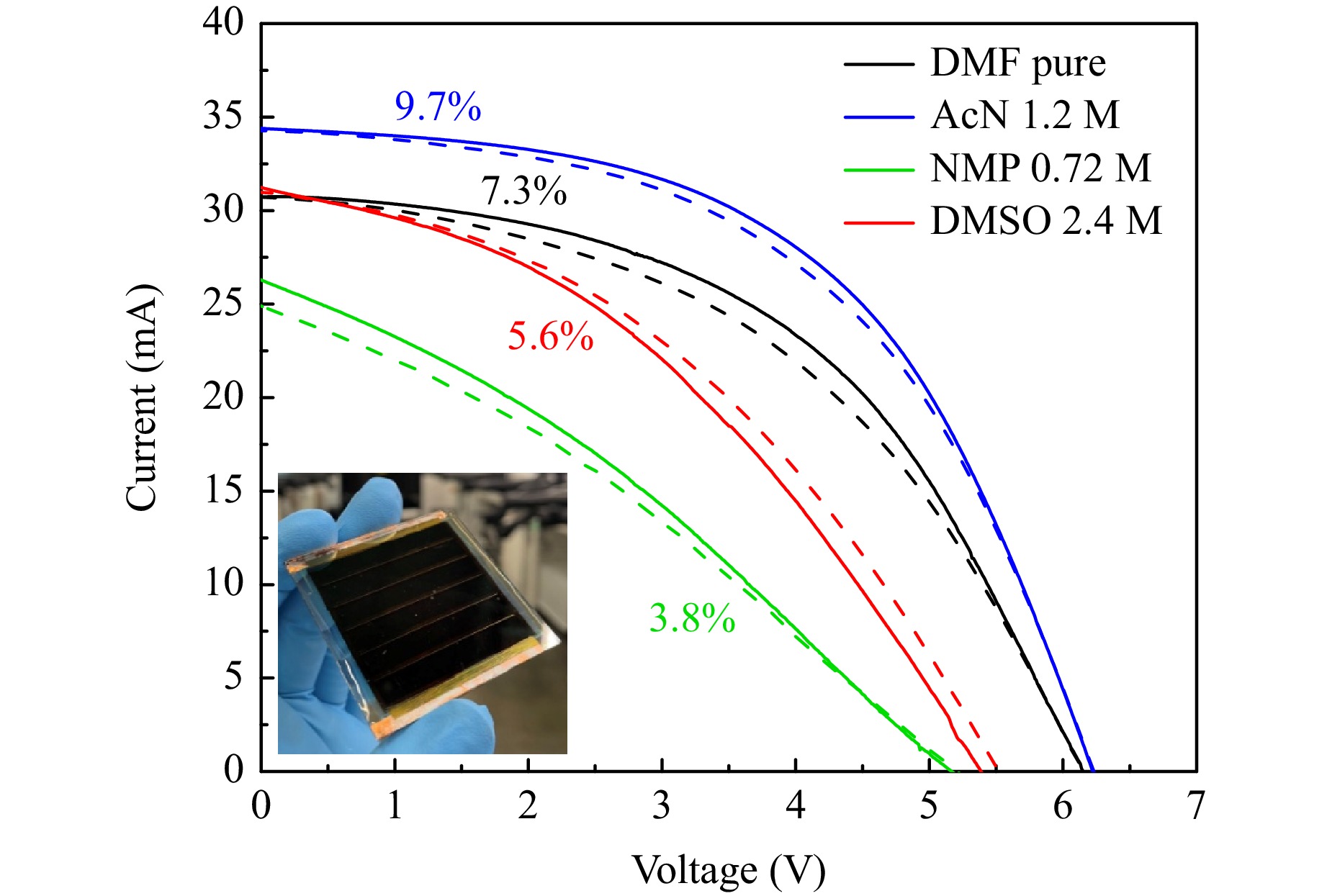
Fig. 7 J-V curves for perovskite mini-modules of total size 25 cm2 with effective area 13.2 cm2 consisting of total 6 sequentially connected cells 2.2 cm2
In conclusion, we improved the device characteristics, stability and suitability for large-scale processing. We utilized conventional perovskite solvent DMF and three additional solvents DMSO, NMP and AcN. It was revealed that implementing of all three leads to the increase of laboratory device efficiency, but the necessary concentration is unique for every solvent. We also were able to assume various processes behind the improvement mechanisms. DMSO addition improves overall quality of the film, increases the perovskite grain size and thickness while producing the “wrinkled” surface. Improved film quality leads to the growth in free charge carrier concentration. However, simultaneously the interface between the perovskite and CTL suffers from the increased interface recombination and worsened adhesion to the HTL. NMP is the solvent with the least visible effects on perovskite film quality, since some defects are still present in the film. However, unlike DMSO, it doesn’t impair the CTL-perovskite interfaces. And implementation of AcN gave unwittingly interesting results. It significantly improved the bulk film quality, morphology and adhesion to ETL, but carrier traps were presumably the cause of low efficiency. However, this solvent demonstrated the best predisposition for upscailing, allowing us to produce 25 cm2 modules with efficiency 9.7%. We also assume that problems with interface are related to the carrier traps accumulation. So the further improvement of such material is possible with advanced analysis of the carrier traps nature and appropriate passivation approach. We also would like to point out the further necessity to find the best CTLs (especially ETL) for this perovskite to ensure its stability and increase efficiency.
-
Materials Cesium iodide (CsI, 99.9%), lead (II) bromide (PbBr2, ≥ 98%), poly[bis(4-phenyl) (2,4,6-trimethylphenyl) amine (PTAA) and vanadium (V) oxide (V2O5, 99.95%) were purchased from Sigma-Aldrich. Other materials were purchased from different companies: lead (II) iodide (PbI2, Chem synthesis), tin (IV) oxide nanoparticles (SnO2, 15% in H2O colloidal dispersion, Alfa Aesar).
Formamidinium iodide ((NH2CH=NH2)I or FAI) was synthesized by the procedure described in Ref. 41; 6,6-phenyl-C61 butyric acid (PCBA) was synthesized by the procedure described in Ref. 42.
Sample fabrication The Cs0.17FA0.83PbI1.8Br1.2 solution was prepared by mixing CsI, FAI, PbBr2, PbI2 in a corresponding stoichiometry ratios. The mixed powders were then fully dissolved in DMF to get 1.5 M mother liquor. To obtain required binary solvent systems a mother liquor was diluted by the corresponding amount of DMF-X mixture (X = DMSO, NMP, AcN) so that the final concentration of perovskite would be 1.2 M. For instance, to make 1 ml of 1.2 M DMSO solution, 114 μl of DMF and 86 μl of DMSO would be added to the 800 μl of mother liquor. The solutions would be left overnight before spin-coating.
Thin films of perovskite were prepared by spin-coating deposition method at the 3000 rpm followed by ethyl acetate anti-solvent deposition. Then all films were heated for 10 min at 120℃ for DMF:DMSO films and 100℃ for all other solvents. The entire process was performed in a N2 glovebox (H2O < 0.1 ppm and O2 < 0.1 ppm).
For n-i-p solar cell preparation, the ITO substrates were sequentially cleaned via sonication in deionized water, acetone and isopropanol followed by a 10 min air plasma treatment. To form the ETL a 10% SnO2 solution was deposited by spin-coating in ambient conditions at 5000 rpm and annealed at 175℃ for 30 min. After that the substrates were transferred to a N2 glovebox, where all the following manipulations were performed. The substrates were annealed at 150℃ for 10 min. After that 0.2 mg/ml PCBA (Phenyl-C61-butyric Acid) solution in chlorobenzene was applied by spin-coater at 3000 rpm and annealed at 100℃ for 10 min. After that the perovskite layer was deposited as described above. Then to make the hole-transport layer (HTL), firstly hot (75-80℃) PTAA (poly[bis(4-phenyl)(2,4,6-trimethylphenyl)amine) solution (15 mg/ml in chlorobenzene) was deposited on a spinning substrate at 4000 rpm. Thermal evaporation was then used to deposit 30 nm of VOx and either 150 nm of Al (for regular devices) or 120 nm of Ag (for the devices used for the EQE measurement).
For mini-module processing we performed photoresist etching of ITO to get a specific pattern for transparent electrodes (P1 line). Then SnO2, PCBA, perovskite, PTAA and VOx layers were deposited with the same processing methods as for laboratory devices. Then we created the P2 line over all deposited layers by mechanical scratching with a scalpel and deposited 150 nm of Al as top electrodes through the shadow mask to ensure the P3 line.
-
The devices were tested using an AM 1.5G simulator (Newport Verasol AAA solar simulator and Advantest 6240 A source-measurement units) in a N2 glovebox.
External quantum efficiency (EQE) measurements were performed utilizing a Newport Oriel IQE200 with chopped light at a frequency of 72 Hz.
X-ray Diffraction (XRD) of the perovskite films was measured on air with an X-ray diffractometer Bruker D8 Advance with CuKα X-ray source and LYNXEYE XY detector, under the θ/2θ mode with 40 kV and 200 mA power conditions.
Steady-state PL and PL mapping experiments were performed on custom LBIC+PL+EL microscopy setup from an Automatic Research GmbH with a Horiba spectrometer. Excitation was done by a 2.5 µW power 535 nm laser.
Absorbance spectra of the perovskite films in the UV-visible region were measured using an Avantes AvaSpec-HS2048 dual-channel optical spectrometer.
Time-resolved PL measurements was performed with time correlated single photon counter (TCSPC) technique on Horiba QuantaMaster spectrofluorometer. Peak emission was set up to 730 nm, entrance slit 5 nm, time range 1.6 μs, 1000 counts for peak channel. Excitation power density – 2.54 nJ/cm2 and the excitation source – diDiode 345 nm. The excitation source was first going through the perovskite material and then through the substrate glass, that excludes the impact of gamma-ray-induced substrate darkening.
The morphology of the perovskite films was characterized using an atomic force microscope (AFM) (NANOEDUCATOR, NT-MDT, Moscow, Russia). The film thickness was measured using AFM microscopy while scanning a thin scratch on the top of the films.
The SEM and Cross-SEM images were obtained on Dual beam scanning electron microscope Helios G4 Plasma FIB UXe. TLD detector, Probe current 25 pA, Landing voltage 5 kV. To study the multilayer structure of sample in the region of interest, a cross-section was performed with an ion beam. To create a cross-section in the region of interest, a protective layer of platinum was deposited using the gas injection method. The area of interest with protective layer of platinum was milled by ion beam, followed by visualization of the cross-section with an electron beam. The assigned images were programmatically reconstructed taking into account the angle between the cross-section surface and the electron beam.
-
For the stability test the perovskite films were applied on glass substrates and covered with PTAA and VOx according to the procedure described in perovskite solar cell fabrication section. The operational stability tests were carried out in a N2 glovebox under simulated AM 1.5G illumination (100 mW/cm2, Class AAA multi-color LED solar simulator, Guangzhou Crysco Equipment Co. Ltd). Absorbance spectra were measured before exposure to sun light and during the stability test, relative change in absorbance of 660 nm wavelength light was plotted to visualize the degradation process occurring in the films.
-
This work was supported by Russian Science Foundation (project No. 23-72-01114). The synthesis of FAI was funded by the Ministry of Science and Higher Education of the Russian Federation (project 122111700041-8).
Enhancing the MA-free mixed halide perovskite efficiency and stability through bi-solvent engineering approach
- Light: Advanced Manufacturing , Article number: (2025)
- Received: 19 June 2024
- Revised: 24 April 2025
- Accepted: 24 April 2025 Published online: 25 July 2025
doi: https://doi.org/10.37188/lam.2025.039
Abstract: Perovskite photovoltaics upholds the most prominent position in the field of tandem technology development. In this aspect, the creation of perovskite material with suitable bandgap (≥ 1.65 eV) is necessary. And in order to achieve the best device characteristics, the high-quality film formation is crucial. To get a high-quality film, the solvent engineering approach stays at the forefront. However, although the solvent engineering was well discussed for such conventional material as MAPbI3, the field of wide bandgap perovskite materials is still lacking in this area. This paper presents the solvent engineering approach to improve the efficiency and stability of the conventional wide bandgap perovskite material Cs0.17FA0.83PbI1.8Br1.2. Here we utilize several solvents such as traditional N,N-dimethylformamide, dimethyl sulfoxide, N-methyl-2-pyrrolidone and acetonitrile. It was demonstrated that implication of any binary DMF-X solvent improves the solar cell efficiency compared to the pure DMF solution, but the ratio of the X solvent is unique for every X and the foundation for the X influence is also unique. The addition of 2.4 M of DMSO is considered the best to improve the stability and efficiency of laboratory devices, however implementation of AcN allowed to produce 25 cm2 mini-modules with the PCE reaching 10%.
Research Summary
How solvents impact multicomponent halide perovskite film formation
Halide perovskites with multination and multination composition are promising materials for new photovoltaic applications. However they are poorly investigated in the field of solvent influence on film production and device quality. Olga R. Parfenova from Russia’s Skoltech Institute and colleagues now present the systematic study of the solvent engineering approach to improve the efficiency and stability of the material Cs0.17FA0.83PbI1.8Br1.2. Besides the widely used N,N-dimethylformamide they utilized three co-solvents: dimethyl sulfoxide, N-Methyl-2-pyrrolidone and acetonitrile. They assumed various mechanisms behind the each solvent influence on device characteristics. And the team was also able to use DMF:AcN mixed solvent create the 25 cm2 perovskite mini-module with efficiency 9.7%, thus proving that it is the most perspective combination for future development of upscailing methods.
Rights and permissions
Open Access This article is licensed under a Creative Commons Attribution 4.0 International License, which permits use, sharing, adaptation, distribution and reproduction in any medium or format, as long as you give appropriate credit to the original author(s) and the source, provide a link to the Creative Commons license, and indicate if changes were made. The images or other third party material in this article are included in the article′s Creative Commons license, unless indicated otherwise in a credit line to the material. If material is not included in the article′s Creative Commons license and your intended use is not permitted by statutory regulation or exceeds the permitted use, you will need to obtain permission directly from the copyright holder. To view a copy of this license, visit http://creativecommons.org/licenses/by/4.0/.

 DownLoad: