


-
Optical security, which modulates light through micro-nano structures to provide specific visual effects for authentication, has been widely used for anti-counterfeiting and information encryption1–3. According to the form of the visual effects, an optical security identifier can be divided into structural patterns and holograms. Structural patterns exhibit colorful4,5 or grayscale6 images under white light that are easy to identify and possess decorative functions. Holograms are typically composed of irregularly arranged pixels that cannot produce meaningful images under white light, whereas they can project holographic images under irradiation with laser beams7,8. Therefore, holograms have the advantages of concealment and difficulty of imitation.
To improve the security and difficulty of imitation, multiplexing, which combines various security schemes into one identifier, has become the development direction for anti-counterfeiting. Multiplexed structural patterns9–11 and holograms12–14, with imaging information that can change with detection conditions, have been proposed. In addition, multiplexed holographic patterns15,16, which appear as printings under incoherent illumination while projecting holographic images under coherent illumination, have attracted considerable attention because of the combined advantages of aesthetics and concealment from structural patterns and holograms. Furthermore, holographic multiplexing, such as polarization multiplexing17, wavelength multiplexing18–20, or angular momentum multiplexing21–23, can be integrated into holographic patterns, which further improves the information carrying capacity and ensures secure encryption.
Holographic patterns require the structures of pixel units to simultaneously tailor two properties of light, including the amplitude, phase, and spectrum, to realize the dual-function. Therefore, strict requirements have been proposed for the optical responses of structural units. Currently, holographic patterns are mainly realized using metasurfaces, with subwavelength structure units that have a powerful capability to control light waves at the nanoscale level24. As a robust resonant and wide-angle nonlinear optical device, the design of chiral holograms25,26 presents novel challenges and stringent requirements for the fabrication of three-dimensional (3D) microstructures. However, the fabrication of metasurfaces typically depends on nano-processing methods, such as electron beam lithography or focused ion beam etching27–33. While these processing techniques offer high precision; for example, Electron Beam Lithography (EBL) can achieve a processing accuracy < 10 nm and Focused Ion Beam (FIB) can attain a patterning precision of approximately 100 nm; they necessitate a high-vacuum environment and involve complex procedures including pattern transfer, etching, and resist removal, which render them relatively expensive and restrict their practical application. In comparison, femtosecond laser processing is a maskless and flexible method for fabricating micro-nano structure arrays on a large scale34–37. Holographic patterns fabricated using femtosecond lasers have been reported, such as polarization-multiplexed holographic patterns consisting of cross-nano structures with arm shapes that were modulated through femtosecond pulses38, or holographic color prints achieved by arraying phase-spectrum controllable elements that were fabricated through femtosecond laser-induced two-photon polymerization39. Furthermore, the three-dimensional processing capability of femtosecond lasers offers an enhanced approach for applications such as chiral holograms40, which require high precision in the three-dimensional morphology of microstructures. Although femtosecond laser processing facilitates the fabrication of holographic patterns, the sophisticated structure of pixel units and the laser direct-writing method still require a long time to fabricate holographic patterns on a large scale39. Novel holographic pattern design methodologies are required, which modulate light through simple structures.
The three-dimensional processing ability of femtosecond lasers enables them to process structures inside materials41 instead of fabricating coplanar structures with different optical responses by carefully tuning their geometric parameters. Therefore, employing the geometric difference of structures processed on different planes of transparent materials will provide another method for achieving optical modulation contrast42. In this study, multiplexed holographic patterns consisting of double-layer structures formed by microholes and microvoids fabricated on the surface and interior of polymethyl methacrylate (PMMA), respectively, are proposed. To improve the fabrication efficiency and guarantee alignment between the two layers, dynamic 3D spatial optical modulation combined with serial stitching, which can realize the rapid fabrication of large-area multi-layered patterns, is used to synchronously process the microhole and microvoid arrays. The fabricated holographic patterns appear as dynamic grayscale images when viewed under white light at different angles, while projecting holographic images under irradiation with laser beams. Furthermore, after transforming the microholes into microcraters via ultrasonic treatment, the holographic images can be changed by filling the microcraters with silicone oil, with a refractive index similar to that of PMMA. These reconfigurable holographic patterns provide multi-channel multiplexing for optical security enhancement, which has significant application potential in anti-counterfeiting and information encryption.
-
The design concept of holographic patterns originated from 3D multilayer patterns. As shown in Fig. 1, a planar 2D pattern can be divided into multiple zones based on geometric features. A 3D multilayer pattern can be achieved by separating the different zones at equal intervals along the z-axis direction. There is no spatial overlap between the layers of the 3D multilayer pattern such that its projection in the z-axis direction is the original 2D pattern. The 2D pattern shown in Fig. 1 is divided into four zones; therefore, the layered 3D pattern consists of four layers. The colored area in each layer of the 3D pattern corresponds to the zone of the 2D pattern, and the colorless area is the blank area without any pattern. Compared with a 2D pattern, the processing of a 3D multilayer pattern using a femtosecond laser requires the movement and location of the laser focus along the optical axis, which not only increases the processing time but also mandates higher requirements for the optical path alignment and motion accuracy of the sample-moving stage. Therefore, improving the processing efficiency and guaranteeing the relative position accuracy between each layer are of great significance in promoting the practical application of 3D multilayer patterns.
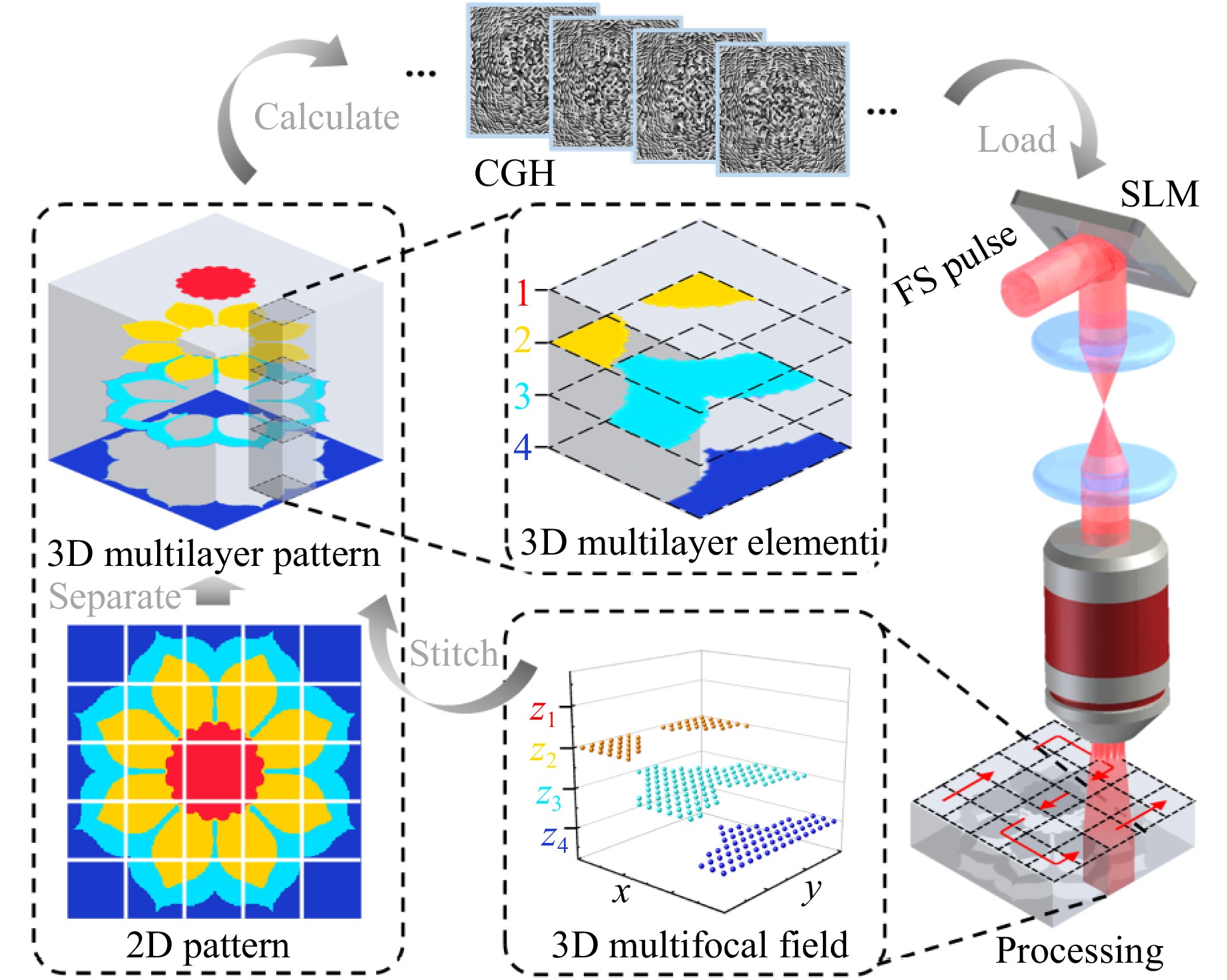
Fig. 1 Schematic of the dynamic 3D spatial optical modulation combined with serial splicing to fabricate 3D multilayer patterns. A 2D pattern containing four zones is split into 25 elements. After separating the four zones at equal intervals along the z-axis direction, the 2D pattern is transformed into a 3D multilayer pattern with 3D multilayer elements that are regarded as target modulated 3D optical fields. By switching the calculated CGHs loaded on to the SLM and moving the sample synchronously, multilayer lattice structures processed using the dynamic 3D multifocal fields are serially stitched together, composing the complete 3D multilayer pattern.
To overcome the aforementioned challenges, dynamic 3D spatial optical modulation combined with serial stitching is proposed to fabricate 3D multilayer patterns with high efficiency. In the proposed method, in addition to being divided into different zones, the 2D pattern is spilt into N2 elements13,43. After separating the zones along the z-axis, each 2D element is transformed into a 3D multilayer element. The 2D pattern shown in Fig. 1 is split into 25 elements, and the local enlarged view of the 3D layered patterns shows the 3D multilayer elements. Each 3D multilayer element then appears as a 3D optical field, with the color pixels corresponding to the foci and the blank area corresponding to the zero-intensity background. A computer-generated hologram (CGH) of each 3D optical field is calculated using the 3D Gerchberg-Saxton (GS) algorithm44. By loading CGHs onto a spatial light modulator (SLM), the phase of the incident laser pulse is modulated, which shapes the single laser focus into a 3D multifocal field. Multilayer lattice structures can be processed in situ inside a material using a 3D multifocal field without moving the laser focus. By switching the loaded CGH and programmatically moving the materials in the XY plane, different multilayer lattice structures are individually processed and serially stitched to form a complete 3D multilayer pattern. The proposed method not only significantly improves the processing efficiency but also avoids alignment between different layers, which realizes high-efficiency and high-quality processing of large-area multilayer patterns.
Fig. 2 shows the multilayer pattern processed using PMMA. The multilayer pattern consisted of six layers of zones with an interval of 10 μm, and the corresponding 2D pattern contained 300 × 300 px with a pixel size of 4 μm (Figure S1, Supporting Information). Therefore, the length of the fabricated pattern was 1.2 mm, which is sufficiently large to be recognized by the naked eye. Owing to the limited area of the focally modulated optical fields, the pattern was spilt into 900 elements. Thus, each 3D multilayer element contained 10 × 10 × 6 px and the value of each pixel was either zero or one. A pixel with a value of one corresponds to the focus in the 3D multifocal field. In the processing of the multilayer pattern, the first layer of the 3D multifocal fields was located on the surface of the PMMA and the other layers were inside the material. Every multilayer lattice structure was processed using a single pulse of 20 μJ. After loading the calculated 900 CGHs in sequence, a multilayer patterned-arranged period structures was fabricated. Fig. 2b, c show optical microscope images of the two local areas of the fabricated multilayer period structures. Area 1 contained layers corresponding to zones 1-3 in the multilayer pattern, and area 2 contained layers corresponding to zones 4-6. The structure arrays of each layer had the same period of 4 μm and the structures around the array edge between different layers had accurate alignment. A complete optical microscopy image of the fabricated 3D multilayer pattern is shown in Figure S1 (Supporting Information). From the optical microscope images, it can be seen that the optical transmittance of the structures processed by a femtosecond laser on the surface and interior of the PMMA was lower than that of the pristine area; therefore, the multilayer pattern formed by the periodic structures was a grayscale pattern.
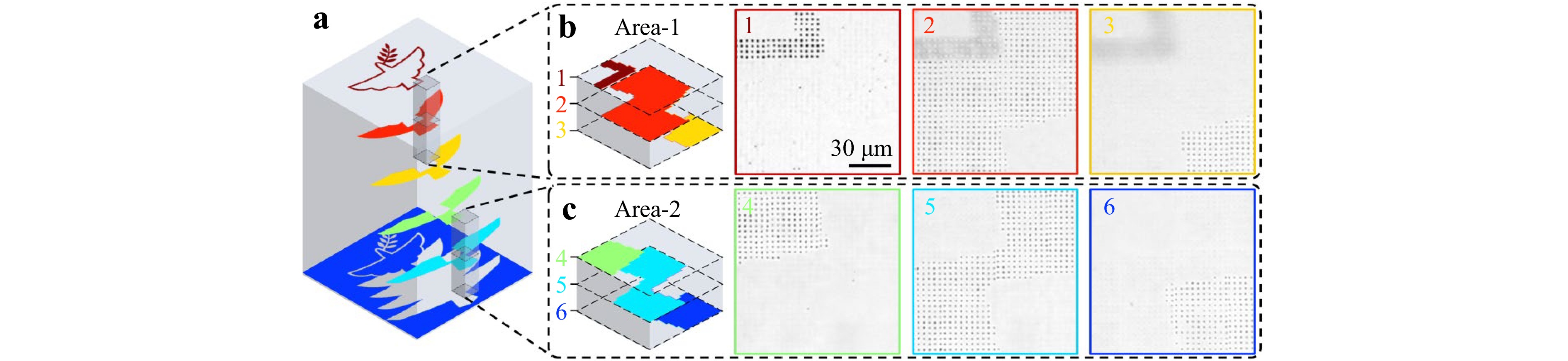
Fig. 2 Morphology characterization of the fabricated 3D multilayer pattern in the PMMA. a Scheme of the 3D multilayer pattern containing six layers of zones. Optical microscopy images of two local areas of the fabricated multilayer pattern containing the zones of b 1-3 and c 4-6. The first layer of the patterned-arranged period structures of the fabricated multilayer pattern was on the surface of the PMMA and the other layers are inside the sample.
-
To further study the morphology and optical properties of structural units in the fabricated multilayer pattern, structure arrays were processed on the surface and interior (10 μm below the surface) of the PMMA using unshaped femtosecond laser pulses to avoid the influence of energy deviation between foci in the multifocal optical fields on the size and morphology of the processed structures. Each structure in the arrays was processed using a single pulse with an energy of 160 nJ. Fig. 3a shows the optical microscopy images of the fabricated structure arrays, containing the detailed morphology of the cross-section (XY plane) and longitudinal section (XZ plane) of a single structure. The structures processed on the surface of the PMMA were conical microholes, while long ellipsoidal voids were formed inside the material. As the ablation threshold of the femtosecond laser on the material surface is typically lower than that inside the material, the diameter of the microhole processed under the same pulse energy was larger than that of the microvoid. Thus, the optical transmittance of the microholes was lower than that of the microvoids, making the microholes appear darker under an optical microscope. Fig. 3b shows the optical transmittances of the pristine PMMA and processed areas with closely arranged microhole and microvoid arrays in the visible spectrum of 500−700 nm. The original PMMA had a transmittance of approximately 0.9 in the visible region; however, after processing the microhole or microvoid array, its transmittance dropped to < 0.2. The transmittance of the microhole array was lower than that of the microvoid array, which was consistent with the direct observation under an optical microscope.
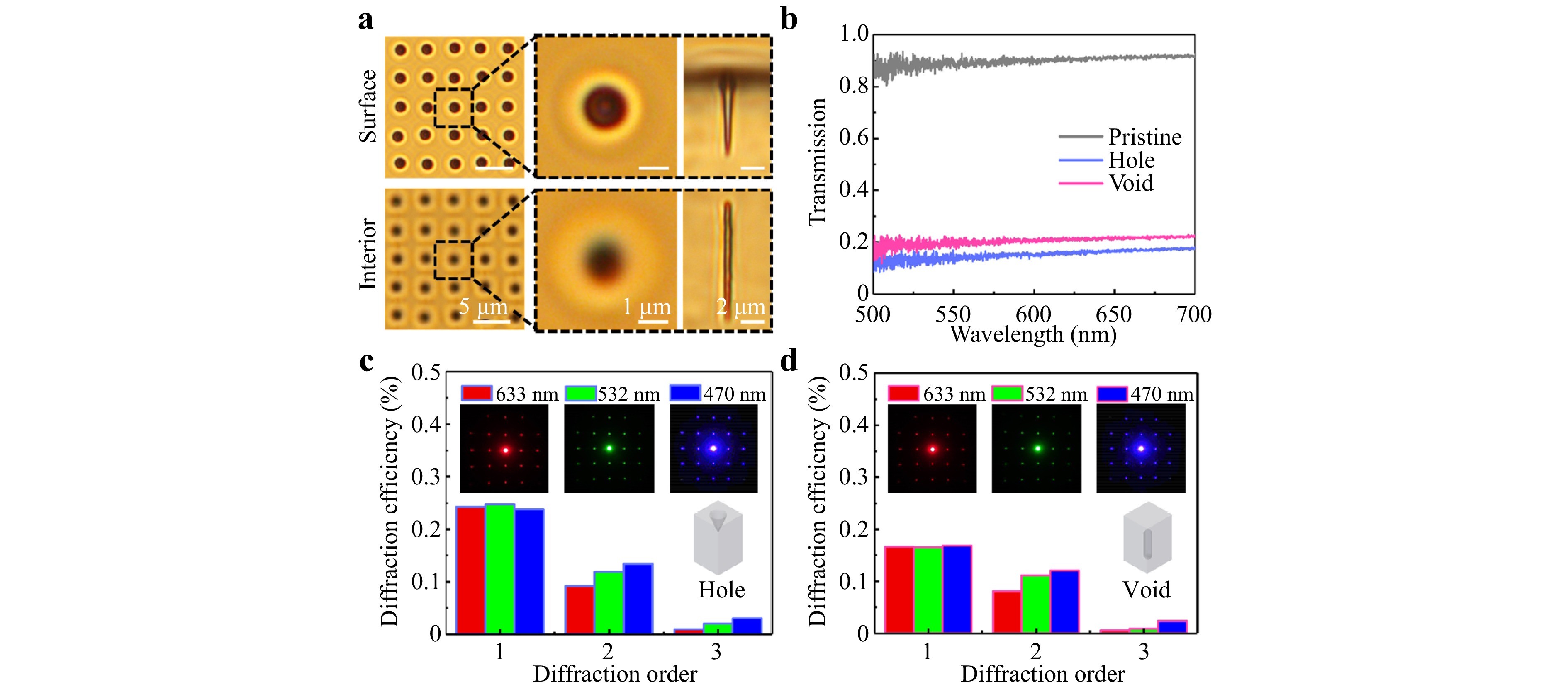
Fig. 3 Morphology and optical property characterization of the structures processed on the surface and in the interior of the PMMA. a Optical microscopy images of the processed microholes on the surface and microvoids in the interior. b Optical transmittances of the pristine PMMA and the processed areas with closely arranged microhole and microvoid arrays. Statistical diagrams of the diffraction efficiencies of different orders in the diffraction patterns of c microhole and d microvoid arrays under irradiation with 470, 532, and 633 nm laser beams. The inset images are the corresponding diffraction patterns.
To reveal the amplitude modulation capability of microholes and microvoids in optical devices, the diffraction characteristics of the structural arrays were measured. The fabricated structure arrays for testing contained 300 × 300 units with a period of 4 μm, shown as 2D gratings. Fig. 3c, d present the diffraction patterns of the microhole and microvoid arrays, respectively, under irradiation with 470, 532, and 633 nm laser beams. The diffraction efficiencies of the different orders of diffraction patterns were also measured. Both structural arrays possessed beam-splitting functions for incident laser beams of different wavelengths. These broadband optical modulation properties agree with the nearly constant optical transmittances shown in Fig. 3b. In addition, the statistical results of the diffraction efficiencies at different wavelengths and orders indicated that the microhole array possessed a higher diffraction capability, which was related to the higher transmittance reduction of the microholes. The transverse dimensions of the microholes and microvoids were approximately 1 μm. Compared to the period of 4 μm, the low filling rate made the diffraction efficiencies of the structural arrays < 1%, but did not affect the recognition of diffraction patterns. Therefore, it was effective to employ microholes and microvoids as amplitude-modulation units to fabricate holograms that could be combined with 3D multilayer patterns to construct multiplexed holographic patterns.
-
The design method for the holographic patterns is shown in Fig. 4a. An image containing the digital sequence— “2.71828...” was selected as the holographic image, and the corresponding binary amplitude hologram was computed by using the 2D GS algorithm. A 2D pattern containing the letter “e” was then selected for the patterning of the hologram. The 2D pattern consisted of two zones located on the surface and in the interior of the sample after separation. In Fig. 4a, the surface and interior zones are represented by the blue and yellow pixels, respectively, and the area outside the zone pattern is filled with black pixels. To perform numerical operations, the hologram and the two patterns were transformed into numerical matrices. The white pixels in the hologram and color pixels in each pattern correspond to a value of one, and the black pixels correspond to a value of zero. Finally, the holograms were multiplied by the corresponding patterns, through which two layers of patterned holograms were achieved. In the implementation of the design scheme, the blue and yellow pixels in the patterned holograms shown in Fig. 4a correspond to the microholes and microvoids in the fabricated holographic pattern, respectively, whereas the black pixels correspond to the pristine area.
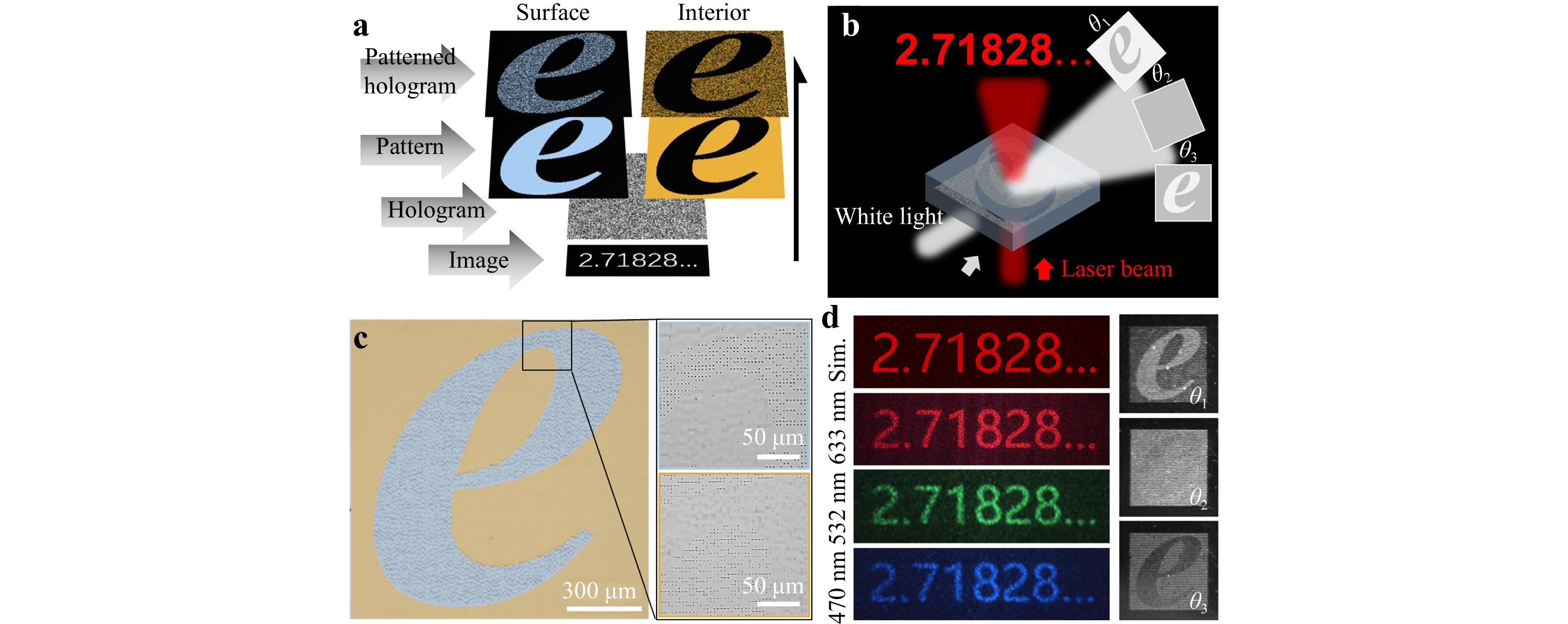
Fig. 4 Design and fabrication of holographic patterns consisting of double-layers of patterned holograms. a Process to design the holographic patterns through calculating the patterned holograms located on the surface and in the interior of the material. All the images contained 300 × 300 px. b Operation scheme of the holographic pattern which presented different visual effects under the illumination of white light and a laser beam. c Optical microscopy images of the fabricated holographic pattern appearing as the letter “e”. The entire image is highlighted in pseudo-color with the blue and yellow areas corresponding to the surface and interior patterned holograms, respectively. d Optical imaging results of the holographic pattern under the illumination of laser beams with different wavelengths (left) and white light with different incident angles (right).
A multiplexing schematic of the holographic pattern is shown in Fig. 4b. The scattering cross-section is related to the angle between the incident light and the structures because the microholes and microvoids scatter the incident light. When observed from a fixed direction, the scattered light of the two structures exhibits different brightness changes with variation in the incident angle. Therefore, under the irradiation of incoherent white light with different angles, the holographic pattern appears as a letter “e” with a dynamic brightness contrast between the surface and the interior patterned holograms and is even presented as a square pattern when the intensities of the scattered light of the two layers are equal. In addition, due to the optical transmittance difference between the pristine material and processed structures (microholes and microvoids), the holographic pattern will project a holographic image of “2.71828...” under irradiation with coherent laser beams.
Based on this design scheme, a holographic pattern was fabricated using dynamic 3D spatial optical modulation, as shown in Fig. 4c. Each layer of the holographic pattern contained 300 × 300 px with a period of 4 μm, and the interval between the surface and the interior patterned holograms was 10 μm. During the processing, the holographic pattern was divided into 900 elements, each of which was processed with a single modulated pulse with an energy of 10 μJ. Although the density of the processed structures in the holographic pattern was approximately reduced to half of that of the period-arranged structures in the multilayer pattern (Fig. 2), the pattern of the letter “e” formed by the arrangement of structures can still be recognized. The transition between the edges of the surface and interior layers is also clear.
Fig. 4d shows the optical imaging results of the holographic pattern. The optical system is shown in Figure S2 (Supporting Information). The left part of Fig. 4d shows the simulated holographic image of the calculated binary hologram and the measured images reconstructed by the holographic pattern under irradiation with laser beams with 470, 532, and 633 nm wavelengths. The measured results were consistent with the simulated results. The right part shows the captured images of the holographic pattern under white light illumination. With changes in the incident angle of white light (Figure S2, Supporting Information), the holographic pattern appeared as a dynamic grayscale image varying from the letter “e” (θ1 ≈ 35°), to a square pattern (θ2 ≈ 55°), to the letter “e” with opposite brightness contrast (θ3 ≈ 75°). The change in the displayed pattern was mainly related to the variation in the scattering cross-section of the microholes and microvoids with the angle of incident light. Near-field images of the holographic pattern under vertical laser beam irradiation were also obtained (Figure S3, Supporting Information). The brightness of the transition edges of the two patterned holograms was slightly lower and there was no obvious intensity difference between the surface and interior patterned holograms. The optical characterization results indicate that the fabricated holographic pattern possesses the expected function, thereby proving the effectiveness of the design scheme.
The design scheme of the holographic pattern shown in Fig. 4a can be regarded as the regional division and separation of the original complete hologram. The reconstructed image of the fabricated holographic pattern agreed well with the simulation result of the complete hologram, without the problem of image ghosting owing to the alignment error of the surface and interior patterned holograms.
However, because patterned holograms consisting of microholes and microvoids record the same image, it is impossible to determine whether the imaging processes of the surface and interior holograms interfere with each other. Thus, a holographic pattern with surface and interior patterned holograms recording different images was designed (Figure S4, Supporting Information). The calculated surface and interior patterned holograms and their simulated imaging results are shown in Fig. 5a, b, respectively. Although patterned holograms contain only a portion of the valid pixels of the original holograms, due to the redundancy of the holograms18,39, clear holographic images can still be reconstructed. Fig. 5c shows the combined hologram obtained by superposing the two patterned holograms with the corresponding simulated holographic images. The superposition of two patterned holograms did not affect their imaging process. The combined hologram could completely reconstruct the images of the two patterned holograms; however, the intensities of the two images were inconsistent. The main reason for this is that the area of the interior zone pattern is larger than that of the surface zone pattern. Therefore, the interior patterned hologram occupies more pixels in the combined hologram. Therefore, in the simulation, the intensity of the image “BIT” reconstructed by the interior patterned hologram was higher than that of the image “1940” reconstructed by the surface patterned hologram.
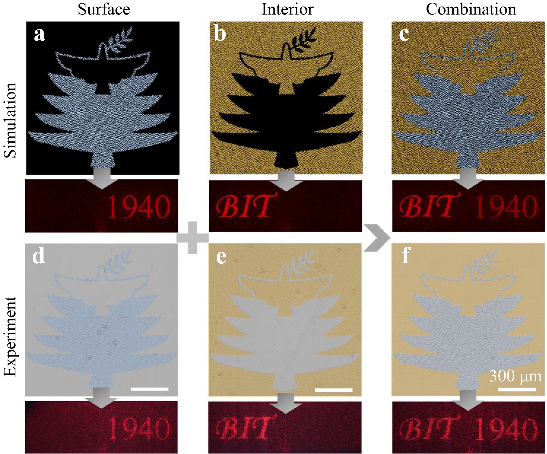
Fig. 5 Fabrication of holographic patterns with surface and interior patterned holograms recording different images. Simulated results of the a surface patterned hologram, b interior patterned hologram, and c combined hologram consisting of the two patterned holograms. Optical microscopy images and reconstructed holographic images of the fabricated d surface patterned hologram, e interior patterned hologram, and f holographic pattern. The microscopy images are highlighted in pseudo-color with blue and yellow areas corresponding to the surface and interior patterned holograms, respectively.
Fig. 5d-f show the fabricated single-layer patterned holograms of the surface and interior and the holographic pattern containing both layers, respectively. The interior patterned holograms lay on a plane 10 μm below the sample surface. The measured holographic images of the single-layer patterned hologram were clear and distinguishable. Furthermore, after being combined into a holographic pattern, the imaging process of the surface and interior holograms did not affect each other. As the structural units of the interior patterned hologram were microvoids, the reduction in optical transmittance was lower than that of the microholes on the surface, and the diffraction efficiency of the interior patterned hologram was lower than that of the surface patterned hologram. Thus, although the interior patterned hologram occupied more pixels in the fabricated holographic pattern, the intensity of the image “BIT” in the measured holographic image was lower than that of the image “1940”. In addition, the influence of the spacing between the interior and surface holograms on the holographic image was studied (Figure S5, Supporting Information). When the spacing was > 50 μm, the intensity of the image “BIT” in the measured holographic image started to decrease. The decrease in the image intensity was related to the size reduction of the microvoids, which was due to focus deformation and the decrease in the peak energy caused by spherical aberration, resulting in a decrease in the diffraction efficiency of the interior holograms. Therefore, to ensure imaging quality, it is necessary to control the layer spacing of the holographic pattern within a reasonable range or introduce spherical aberration compensation to the spatial modulation of femtosecond pulses44,45.
-
Due to the fluidity and refractive index modulation of liquids, adjusting the function of optical devices through liquids has been successfully achieved46,47, such as tuning the focal length of the lens by filling liquids with different refractive indices48, or reversing the direction of reflected light by changing the refractive index gradient of the metasurface by filling with water49. Inspired by these studies, reconfiguring the holographic pattern by filling the surface structures with liquid is proposed to change the holographic image. The scheme is illustrated in Fig. 6a. The optical transmittance reduction of microholes and microvoids is the basis for constructing amplitude holograms. The light incident onto the sample is reflected and refracted on the structural surface of the microholes and microvoids, which causes the light to deviate from the original propagation direction, thereby reducing the transmittance. The reflectivity of the structure surface and the propagation direction offset of the refracted light are related to the refractive index difference between the media on both sides of the interface (structural surface). The smaller the difference in the refractive index, the smaller the reflectivity and offset of the refracted light, which increases the transmittance of the incident light. Therefore, by filling the microholes with a liquid with a refractive index that is similar to that of PMMA, the refractive index difference between the media on both sides of the microhole wall decreases, which improves the optical transmittance of the pixels where the microholes are located. The reduction of the transmittance difference between the microhole pixels and the unprocessed pixels leads to the decrease in diffraction efficiency of the surface patterned hologram, which erases the corresponding image “1940” from the reconstructed holographic image. An interior patterned hologram consisting of microvoids can reconstruct a holographic image. Due to the strong affinity between PMMA and silicone oil, silicone oil with similar refractive index (n ≈ 1.49) to PMMA was selected as the filling liquid.
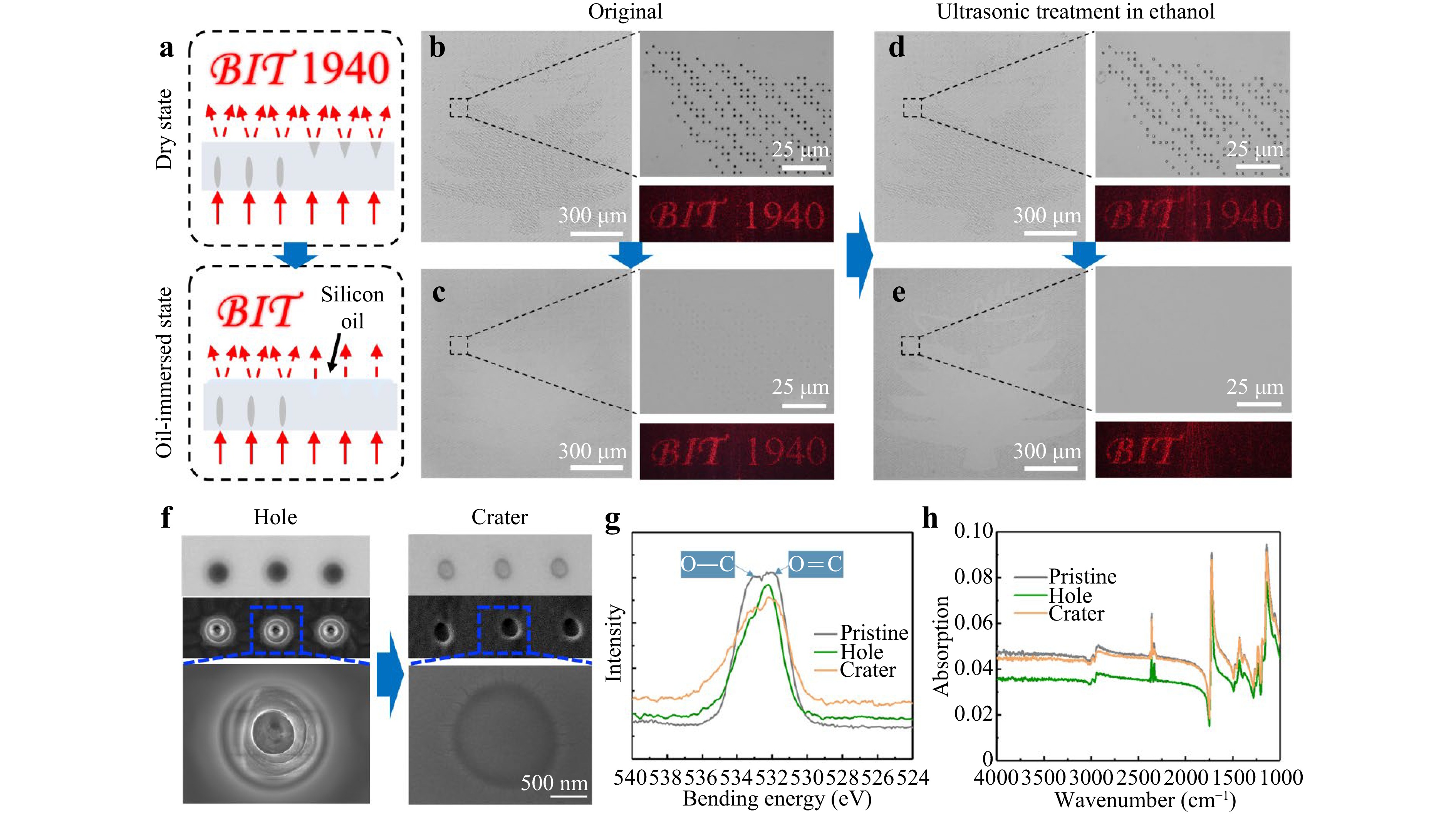
Fig. 6 Reconfiguration of holographic patterns through filling the surface structures with silicone oil. a Scheme of hologram reconfiguration through liquid immersion. By filling the microholes with silicone oil, the holographic image corresponding to the surface patterned hologram is erased from the reconstructed holographic image of the holographic pattern. Optical microscopy images and the corresponding holographic images of the initial holographic pattern in the b dry and c oil-immersed states. Filling with silicone oil cannot completely erase the holographic image “1940”. After ultrasonic treatment for 5 min, the optical microscopy and reconstructed images of the holographic pattern in the d dry and e oil-immersed states. In this situation, the image “1940” is almost indistinguishable after filling with silicone oil. f Optical microscopy images and SEM images of the microhole array before and after ultrasonic treatment. The gully structures on the inner surface of microholes can be smoothed through ultrasonic treatment, which transforms the microholes into microcraters. g XPS spectra in the O1s region (524−540 eV) of the pristine PMMA, microholes, and microcraters. h Infrared spectra of the pristine PMMA, microholes, and microcraters under a wavenumber range of 4000−1000 cm−1.
Fig. 6b, c show optical microscopy images of the holographic pattern and corresponding holographic images in the dry and oil-immersed states, respectively. After filling the microholes with silicone oil, the brightness of the surfacepatterned hologram increased, illustrating the effectiveness of the silicone oil for transmittance enhancement. However, from the locally enlarged image, transmittance reduction of the microholes still occurred. Therefore, the image “1940” corresponding to the surface patterned hologram could still be distinguished, although its intensity decreased. In this situation, filling with silicone oil cannot completely erase the holographic image of the surface patterned hologram.
In the femtosecond laser ablation of the material, the generated debris may attach to the inner wall of the microholes, making the inner surface of the microholes rough. In addition to trapping incident light and reducing optical transmittance, the rough surface hinders the infiltration and microhole filling of silicone oil. To verify this hypothesis, the holographic pattern was cleaned in ethanol using ultrasound before being immersed in oil. As PMMA can easily to produce cracks during ultrasonic cleaning in ethanol, to reduce the generation of cracks the fabricated holographic pattern was maintained at 80℃ for 30 min before ultrasonic treatment to fully release the interior stress. The optical microscopy and holographic images of the holographic pattern after ultrasonic treatment for 5 min are shown in Fig. 6d. The optical transmittance of microholes was improved after ultrasonic treatment; therefore, the intensity of the holographic image “1940” was reduced due to the decrease in the diffraction efficiency.
After immersion in silicone oil, as shown in Fig. 6e, the brightness of the surface patterned hologram was almost the same as that of the pristine surface, and the microholes were hardly distinguishable, even in the local enlarged image. Therefore, the microholes filled with silicone oil have a limited effect on the optical transmittance of the material. In this case, only the image “BIT” reconstructed by the interior hologram remained in the holographic image, and the image “1940” was almost indistinguishable. The experimental results show that ultrasonic pretreatment contributes to the optical transmittance enhancement of microholes by filling the liquid, which successfully realizes the reconfiguration of the holographic pattern and the variation of the holographic image. To explore the effect of ultrasonic pretreatment, the same ultrasonic treatment was also performed on the periodic microhole array processed by unshaped femtosecond laser pulses.
Optical microscopy and scanning electron microscopy (SEM) images of the microhole array before and after the treatment are shown in Fig. 6f. Before the ultrasonic treatment, the inner surface of the microholes was not smooth, and there were many gully structures on the surface. The gully structures scatter and trap incident light and hinder the flow of silicone oil into the microholes. After the ultrasonic treatment, the gully structures inside the original microholes disappeared, and the inner surfaces of the structures became smoother. The atomic force microscopy characterization results further indicated that the microholes were transformed into microcraters after ultrasonic treatment (Figure S6, Supporting Information). Microcraters with smooth inner surfaces improved the optical transmittance of the original microholes (Figure S7, Supporting Information), as indicated by the brightness enhancement of the structures in the optical microscopy image. Therefore, instead of removing the debris from the interior surface of the microholes, the ultrasonic treatment of the structure morphology smoothed the gully structures on the inner surface.
In addition to the morphology, the chemical components on the surface of the structure also affect the optical transmittance and affinity between the material and liquid. To explore whether femtosecond laser processing and ultrasonic treatment can modify the chemical composition of PMMA, the surface chemical characteristics of the microholes and microcraters were analyzed. Fig. 6g shows the X-ray photoelectron spectroscopy (XPS) spectra of O1s conducted for the pristine PMMA, microholes, and microcraters. There were two peaks in the O1s spectrum of the initial PMMA, which corresponded to the C-O (533.2 eV) and C = O (532 eV) bonds, respectively. The two peaks merged in the spectrum of the microholes. However, after ultrasonic treatment, the single peak split into the two original peaks in the spectrum of the microcraters. There are two explanations for the merging of the two peaks in the O1s spectrum of the PMMA after laser processing. The first attributes such a phenomenon to the degradation of the free methyl formate radical into methane and carbon oxide in laser ablation50. Based on this explanation, new functional groups were produced on the surfaces of the microholes. During the ultrasonic treatment, the functional groups were removed. However, from the infrared absorption spectrum shown in Fig. 6h, no new spectral peak or peak ratio change was observed in the spectrum of the microholes or microvoids, indicating that femtosecond laser processing and ultrasonic treatment had no impact on the chemical composition of PMMA. Another explanation is that the merging of the two peaks in the O1s spectrum originates from wider electron scattering from the rough surface of PMMA51. Therefore, the splitting of the spectral peak after the ultrasonic treatment can be attributed to a reduction in the surface roughness. This explanation and deduction are consistent with the morphological characterization results of the microholes and microcraters.
From the morphological and chemical characterization results, it can be deduced that the optical transmittance reduction of the microholes was mainly due to the scattering and trapping effects of the structures on the incident light, rather than the change in chemical composition. This deduction is also applicable to microvoids inside the material. In addition, the ultrasonic pretreatment changed the original microholes with rough surfaces into microcraters with smooth surfaces, which favored the filling of the surface structures with silicone oil. Therefore, the holographic pattern can be successfully reconfigured by reducing the refractive index difference between the media on both sides of the structural interface.
-
A novel design methodology for multiplex holographic patterns employing layered microholes and microvoids as structure pixels was proposed. Using dynamic 3D spatially modulated femtosecond pulses, holographic patterns consisting of double layers of structural arrays with sizes visible to the naked eye can be rapidly fabricated. The difference in light scattering between the microholes and microvoids enables the holographic patterns to appear as attractive dynamic grayscale images when viewed under white light at different angles. The optical transmittance difference between the processed structures and the pristine area endowed the holographic patterns with holographic imaging capabilities. Furthermore, by transforming microholes into microcraters via ultrasonic treatment, the holographic images can be varied by filling the microcraters with silicone oil, which can be used to encrypt additional information. Holographic patterns possess both the artistry of prints and the concealment of holographic projections, which can be reconfigured through refractive index modulation using liquid immersion. The proposed multi-channel multiplexing provides the proposed holographic patterns with extensive potential for anti-counterfeiting and optical encryption.
-
A schematic of the femtosecond laser processing system is shown in Fig. 1. A commercial Ti:sapphire laser regenerative amplifier system (Spitfire Ace-35F, Spectra Physics, USA) with a 35 fs pulse duration, 800 nm central wavelength, and 1 kHz repetition rate was used to provide femtosecond laser pulses, with power and pulse numbers that were adjusted by a neutral density attenuator and a mechanical shutter, respectively. After the laser pulses were shaped by a reflective liquid-crystal-on-silicon SLM (8 μm pixel pitch, 1920 × 1080 px resolution, Pluto-NIR, Holoeye, Germany), the modulated pulses were delivered through a 4 f (f = 600 mm) optical system and focused by an objective lens (20×, NA = 0.45). The 3D multifocal optical fields were formed in the PMMA (3 mm thick, 87℃ thermal deformation temperature) with the first layer of multifocal arrays on the PMMA surface. The PMMA was mounted on a six-axis moving stage (M-840.5DG, PI, USA), which was synchronously controlled with a shutter and SLM using home-built software.
-
Before the ultrasonic treatment, the fabricated holographic pattern was heated in a furnace. The temperature of the holographic pattern was increased from room temperature to 80℃ in 30 min and maintained for another 30 min, after which the holographic pattern was slowly cooled with the furnace.
-
Optical microscopy and SEM images of the fabricated structures were obtained using an optical microscope (BX53, Olympus, Japan) and a field-emission scanning microscope (SU8200, Hitachi, Japan), respectively. Atomic force microscopy (Dimension Edge PSS, Bruker, USA) was used to characterize the 3D morphology of the microcraters. The optical transmittance spectra (wavelength range of 500–700 nm) and the infrared spectra (wavenumber range of 4000–1000 cm−1) were obtained through a Fourier transform spectrometer (Excalibur 3100, Varian, USA). The X-ray photoelectron spectra in the O1s region (524–540 eV), realigned relative to the binding energy of C1s (284.8 eV), were recorded using an X-ray photoelectron spectrometer (PHI Quantera II SXM, Ulvac-Phi, Japan). For holographic imaging, the projected images were reconstructed using holographic patterns under irradiation with a supercontinuum laser source (SuperK EXTREME, NKT Photonics, Denmark), with a wavelength tuned to 470, 532, or 633 nm. After focusing through a lens (f = 100 mm), holographic images were captured using a full-color charge-coupled device (Lm11059C, Lumenera, Canada). To capture photographs of the holographic patterns viewed under incoherent white light illumination, the laser source was replaced with an LED lamp mounted on a rotatable arm.
-
The authors thank the National Key R&D Program of China (Grant No. 2022YFB4601300), National Science Fund for Distinguished Young Scholars (Grant No. 52325505), National Natural Science Foundation of China (NSFC) (Grant Nos. 52075041 and U21A20140), Chongqing Natural Science Foundation of China (Grant No. cstc2021jcyj-cxttX0003), Joint Funds of the National Natural Science Foundation of China (Grant No. U2037205), and the Beijing Outstanding Young Scientist Program (Grant No. BJJWZYJH01201910007022).
Reconfigurable holographic patterns for optical security multiplexing fabricated by 3D spatially modulated femtosecond pulses
- Light: Advanced Manufacturing , Article number: (2025)
- Received: 11 November 2024
- Revised: 14 April 2025
- Accepted: 19 May 2025 Published online: 05 November 2025
doi: https://doi.org/10.37188/lam.2025.046
Abstract: Holographic patterns that integrate printings and holograms into a single device have received extensive attention in optical security owing to their attractive aesthetics and concealment. However, the sophisticated structures of metasurface-based optical devices require a time-consuming fabrication process, hindering the practical application of holographic patterns in optical security. In this study, a novel double-layer holographic pattern that employs simple microholes and microvoids as optical modulation units is designed and experimentally demonstrated. The two layers of the structure arrays are synchronously processed in a transparent material through a single serial-stitching of dynamic 3D spatially modulated femtosecond pulses that are proposed for the rapid fabrication of large-area multi-layered patterns. The fabricated holographic pattern appears as a dynamic grayscale image under white light incident at different angles and projects encoded holographic images under laser illumination. By transforming microholes into microcraters by ultrasonic treatment, the reconfiguration of the holographic pattern can be realized based on refractive index modulation using liquid immersion. The proposed reconfigurable holographic patterns with simple structures and visible sizes enable the recoding of multiple pieces of information, making them practical optical security elements with a wide range of applications in anti-counterfeiting and information encryption.
Research Summary
Reconfigurable Holographic Patterns Fabricated by 3D Spatially Modulated Femtosecond Pulses
Three-dimensional spatially shaped femtosecond lasers enable efficient fabrication of multilayer reusable patterned holograms in transparent materials with micron-scale precision. These holographic patterns have gained significant attention in optical security applications due to their unique aesthetic versatility and covert information storage capabilities. Professor Lan Jiang from Beijing Institute of Technology and colleagues developed a dynamic three-dimensional spatially modulated femtosecond pulse splicing technique, achieving rapid fabrication of large-area multilayer configurations in dielectric substrates. This advanced methodology facilitates high-throughput production of multiplexed holographic patterns with high alignment accuracy. Refraction modulation holograms can be reconstructed by immersing the surface microstructure in liquid. The proposed reconfigurable holographic pattern exhibits characteristics of a simple structure and visible scale, allowing for the re-encoding of multiple pieces of information.
Rights and permissions
Open Access This article is licensed under a Creative Commons Attribution 4.0 International License, which permits use, sharing, adaptation, distribution and reproduction in any medium or format, as long as you give appropriate credit to the original author(s) and the source, provide a link to the Creative Commons license, and indicate if changes were made. The images or other third party material in this article are included in the article′s Creative Commons license, unless indicated otherwise in a credit line to the material. If material is not included in the article′s Creative Commons license and your intended use is not permitted by statutory regulation or exceeds the permitted use, you will need to obtain permission directly from the copyright holder. To view a copy of this license, visit http://creativecommons.org/licenses/by/4.0/.

 DownLoad: