


-
The application of metasurfaces to control electromagnetic and light waves has garnered increasing research interest1–6. Among the diverse unit cell designs used in metasurfaces, ring-shaped patterns and their variants are popular because of their advantageous properties. For instance, centrosymmetric ring unit cells are generally polarisation-insensitive to incoming wave states7–16, whereas split rings can modify the phase of electromagnetic waves through rotational orientation17–35. Beyond metasurfaces, ring-shaped patterns are the basic units of frequency-selective surfaces36,37, electromagnetic shielding meshes38–40, and concentric circular diffractive optical elements41–43. Consequently, efficient production of high-quality ring-shaped microstructures is valuable for these applications.
Research on metasurfaces and electromagnetic components has focused predominantly on planar substrates. However, nonplanar surfaces are essential in applications requiring multifunctionality, often integrating metasurfaces and involving cylindrical, spherical, freeform, or nonuniform rational B-spline geometries. However, the complexity of fabricating metasurfaces on curved surfaces significantly limits their broad application. Although additive manufacturing techniques44–46 have improved three-dimensional (3D) object construction, metasurfaces still rely on rigid preformed substrates, with the manufacturing process constrained by the surface geometry. In some studies, small planar metasurface sections have been attached to nonplanar geometries, effectively treating them as curved surfaces through segmentation26,47. However, this approach often deviates from the original design, affecting the electromagnetic performance. Flexible conformal substrates that can be stretched onto curved surfaces tend to experience unpredictable deformations under multidirectional bending, limiting their practical applications25,48–53. Thus, developing reliable methods that can be used to produce microstructures directly on curved surfaces is essential for advancing metasurface research and applications.
Direct laser writing lithography (DLWL) enables high-precision exposure and flexibility in pattern formation54,55. Efforts have been made to adapt DLWL to manufacture microstructures on spherical surfaces. For example, Radtke et al. adapted a commercial laser direct-writing system, initially intended for planar lithography, to create concentric circular grids on a convex lens41. Similarly, Ai et al. designed a dedicated exposure system with optical and mechanical components to create meshes on spherical substrates56–58. Fabricating patterns and structures on 3D surface require additional mechanical displacement and rotation, which can introduce positional errors. Additionally, microscope objectives used in conventional DLWL systems for beam focusing have a limited focal depth and working distance59,60. These factors impose more stringent requirements on sophisticated mechanical setups and autofocus systems. However, researchers have not found an effective and economical method to address this challenge, which hinders the advancement of applications on curved surfaces.
Annular lithography61–64, an approach that shapes the laser beam into a ring-shaped spot, enables the entire ring structure to be exposed in a single pulse without mechanical motion. This method achieves high exposure efficiency and eliminates pattern-stitching problems. Knoblich et al. introduced a straightforward annular lithography optical setup that does not require a microscope objective63,64. However, the current annular lithography methods have not yet been applied to micro ring-shaped structures on curved substrates and cannot be used to produce the fine structures required for broader applications.
To overcome these limitations, we propose a novel annular lithography technique for curved surface exposure termed aberration-converged annular lithography (ACAL). This approach utilises the aberration effect of convex lenses to focus a conventional annular beam onto a smaller ring-shaped spot, enabling finer ring-shaped structures to be exposed. This focusing mechanism increases the focal depth, thereby minimising both the defocus blur caused by height variations in the surface profile and mechanical positional errors. The long focal depth and large diameter variation characteristics enable this method to produce high aspect ratios and allow applications to multi-sized systems65,66. Furthermore, this method simplifies the exposure process by generating a ring-shaped pattern in a single laser pulse, which makes it convenient for exposing arbitrarily curved surfaces. The improved processing efficiency and reduced equipment costs render this method highly valuable for practical manufacturing applications.
-
Spherical lens aberration, traditionally considered an optical imperfection, is often corrected through compensatory design adjustments. Although this phenomenon has often been overlooked, it has potential applications in annular lithography. This report presents a novel lithography method that leverages lens aberrations on curved surfaces, as shown in Fig. 1a. This concept is schematically illustrated in Fig. 1b, which shows a typical demonstration of spherical aberration. Although the beam is refracted towards the focal point, there is a slight distance between the positions where each ray intersects the optical axis. The inner beam layers are focused farther than the outer layers. Notably, the beam layers intersect sequentially before focusing. By leveraging this feature, a collimated annular beam can be modulated into a narrow-width, high-intensity, and ring-shaped spot located between the convex lens and focal plane. However, its ring diameter changes significantly over short distances, making it unsuitable for lithography unless the distance is controlled precisely. An effective solution involves inserting optical elements to adjust the incident beam angle before the aberration lens (Lens2), thereby locally aligning the output beam with the optical axis. The emergent beam converges layer-by-layer in this area. This concept broadens the range of beam convergence, enabling a greater focal depth to accommodate fluctuations in the substrate profile.
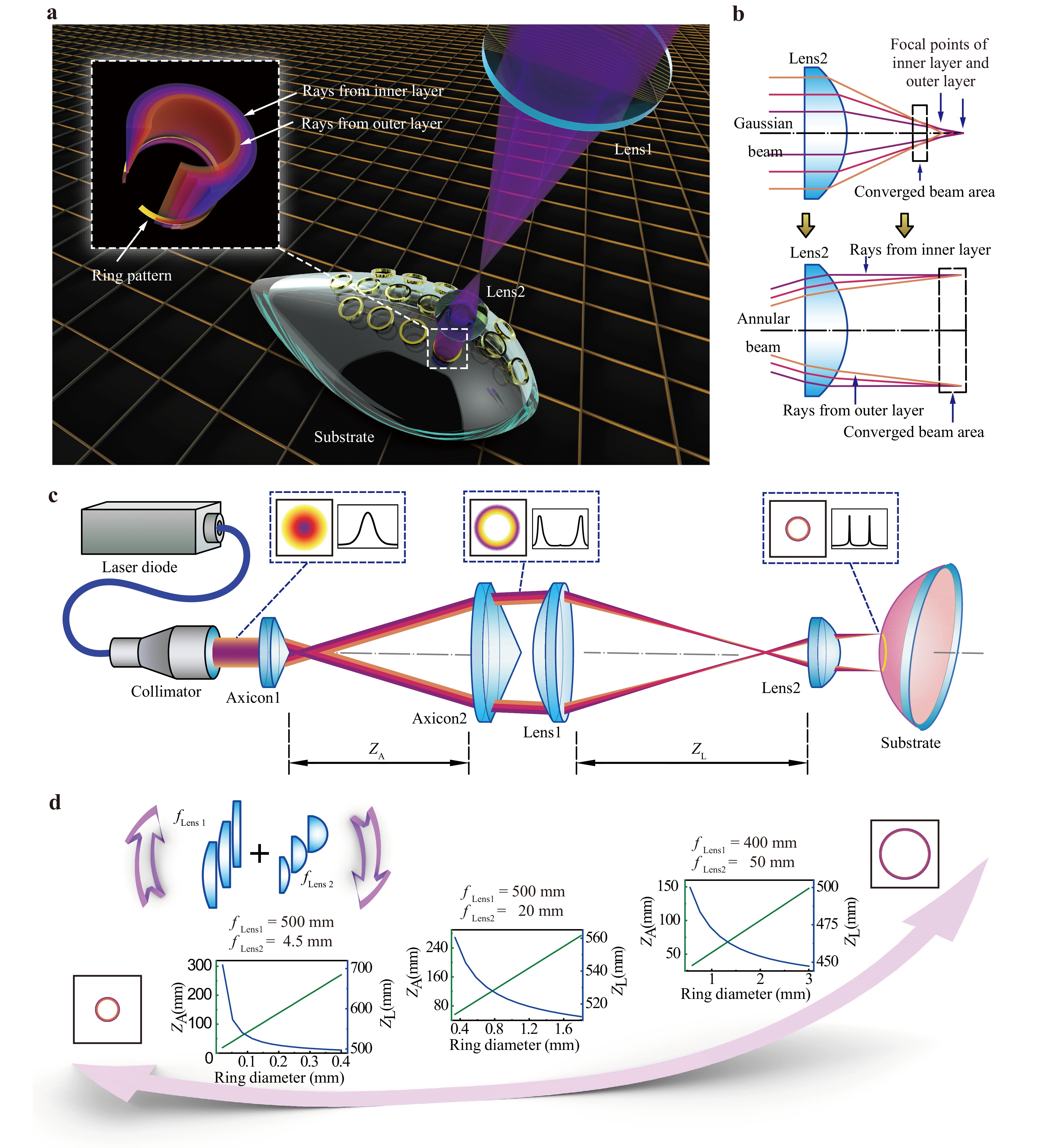
Fig. 1 Optical setup of the ACAL system. a Schematic of the ACAL exposing ring-shaped patterns on a curved substrate and an expanded image detailing the composition of beam layers. b Schematic of the concept behind the ACAL system, with a convex lens converging beam layers through aberration. Changing the incident beam angle can align the converged beam. c Schematic of the annular beam being modulated into an annular converged beam, accompanied with images illustrating the intensity distribution of these locations. d Two methods for adjusting the diameter of the ring pattern: replacing pairs of convex lenses and adjusting the distance of optical elements.
A novel optical setup was proposed to implement this concept, as shown in Fig. 1c. A fibre-coupled UV laser diode emits the incident beam, which is subsequently collimated. The optical setup includes two axicons and two spherical convex lenses. The axicons are placed in front of the optical setup to generate an annular beam. When the beam passes through the first axicon (Axicon1), it is transformed symmetrically into a conical shape. The second axicon (Axicon2) refracts this conical beam and shapes it into a nearly collimated annular beam. The distance between the axicons (ZA) directly influences the diameter of the ring-shaped pattern. The second component, comprising two spherical convex lenses, reduces the diameter of the ring-shaped pattern and narrows the ring width. The first convex lens (Lens1) has a longer focal length than the second, which is arranged behind the focal plane of the first lens. The aberration in the second convex lens (Lens2) is essential for reducing the annular beam width in the radial direction, setting it apart from the Kepler telescope system. Lens aberrations cause the layers of the incident rays to intersect at minimal angles, thereby producing a finer ring pattern. We used Python to simulate the beam-converging process near the image plane, and the results are shown in Fig. S1 in the Supplementary Information.
The spacing between the two convex lenses (ZL) is critical for aligning the output beam and maintaining a consistent ring width. Most rays in this setup are non-paraxial, causing the ring-shaped pattern to deviate from the focal plane, rendering the optical imaging approach inaccurate. A more reliable approach to optimizing optical element positioning involves applying Snell’s law (Eq. 1) to trace rays as they refract from the surface of each lens:
$$ {n_1}\sin {\theta _1} = {n_2}\sin {\theta _2} $$ (1) The Gaussian beam emitted from the laser diode exhibited a higher intensity in its inner layer. In our optical setup, we traced the rays originating from the inner layer of the emission port. They were then adjusted to traverse parallel to the optical axis within the ring-pattern-shaping area. The distance between the axicons (ZA) is calculated as Eq. 2:
$$ A = \arcsin \frac{{{D_{\text{R}}}}}{{2{r_2}}} - \arcsin \frac{{{D_{\text{R}}}}}{{2{n_{\text{C}}}{r_2}}} $$ $$ B = \arcsin ({n_{\text{A}}}\sin {\theta _{\text{A}}}) - {\theta _{\text{A}}} $$ $$ C = {\theta _{\text{A}}} - \arcsin \left[{n_{\text{A}}}\sin \left({\theta _{\text{A}}} - \arcsin \frac{{\sin A}}{{{n_{\text{A}}}}}\right)\right] $$ $$ {Z_{\text{A}}} = \frac{{{r_1}}}{{\tan B}}\sin \left(\arctan \frac{{{n_{\text{C}}}\sin A + \sin C}}{{{n_{\text{C}}}\cos A - \cos C}}\right) $$ (2) where A, B, and C represent parameters within the formula to calculate the distance ZA, DR is the diameter of the expected ring pattern, nA is the refractive index of axicons, θA is the physical angle of axicons, r2 is the radius of the second convex lens, and nC is the refractive index of the convex lenses. Using a similar approach, the distance between the convex lenses (ZL) is given by Eq. 3:
$$ {Z_{\text{L}}} = \frac{{{Z_{\text{A}}}\tan B + {D_{\text{R}}}/2}}{{\tan (\arcsin ({n_{\text{C}}}\sin A))}} - \frac{{\tan A(t{c_1} + t{c_2} - {r_1} - {r_2} + \sqrt {r_1^2 - {{({D_{\text{R}}}/2)}^2}} + \sqrt {r_2^2 - {{({Z_{\text{A}}}\tan B)}^2}} )}}{{\tan (\arcsin ({n_{\text{C}}}\sin A))}} $$ (3) where tc1 and tc2 denote the centre thicknesses of the first and second convex lenses, respectively, and r1 is the radius of the first convex lens. Based on Eqs. 2, 3, two methods exist for adjusting the ring pattern diameter: selecting different pairs of convex lenses and altering the spacing between the optical elements. As shown in Fig. 1d, the ring diameter can be controlled by changing the combination of the first and second lenses. A higher ratio of fLens1 to fLens2 results in a smaller ring pattern. Adjustments in the distances between the optical components enable finer control over the ring diameter, where ZA refers to the axicon distance and ZL is the distance between the convex lenses. In this work, we tested two pairs of convex lenses in our experimental setup to verify the characteristics of the proposed method.
-
The intensity distribution near the image plane was simulated using the ray-tracing method. Fig. 2 presents the results of a typical 0.6 mm diameter ring-shaped pattern, which was simulated using the commercial software ZEMAX Optical Studio. The intensity distribution results were captured close to the image plane, located 31.2 mm from the second lens and colour-coated. Five parallel arrays of cross-sectional images were captured in the x-y plane and a single image in the y-z plane along the beam propagation direction. Each image shows that the intensity distribution of the ring patterns is well preserved and highly contrasted during propagation. Within ±0.2 mm of the image plane, the rays converge to a compact region, suggesting that the simulated ring width is finer than the simulated pixel size of 2 µm. During this interval, the ring diameter remains nearly constant, and the peak intensity is above 90% of the maximum intensity at the image plane. Extending the defocus range to ±1 mm increases the ring width to approximately 8 µm and decreases the peak intensity to 65%.
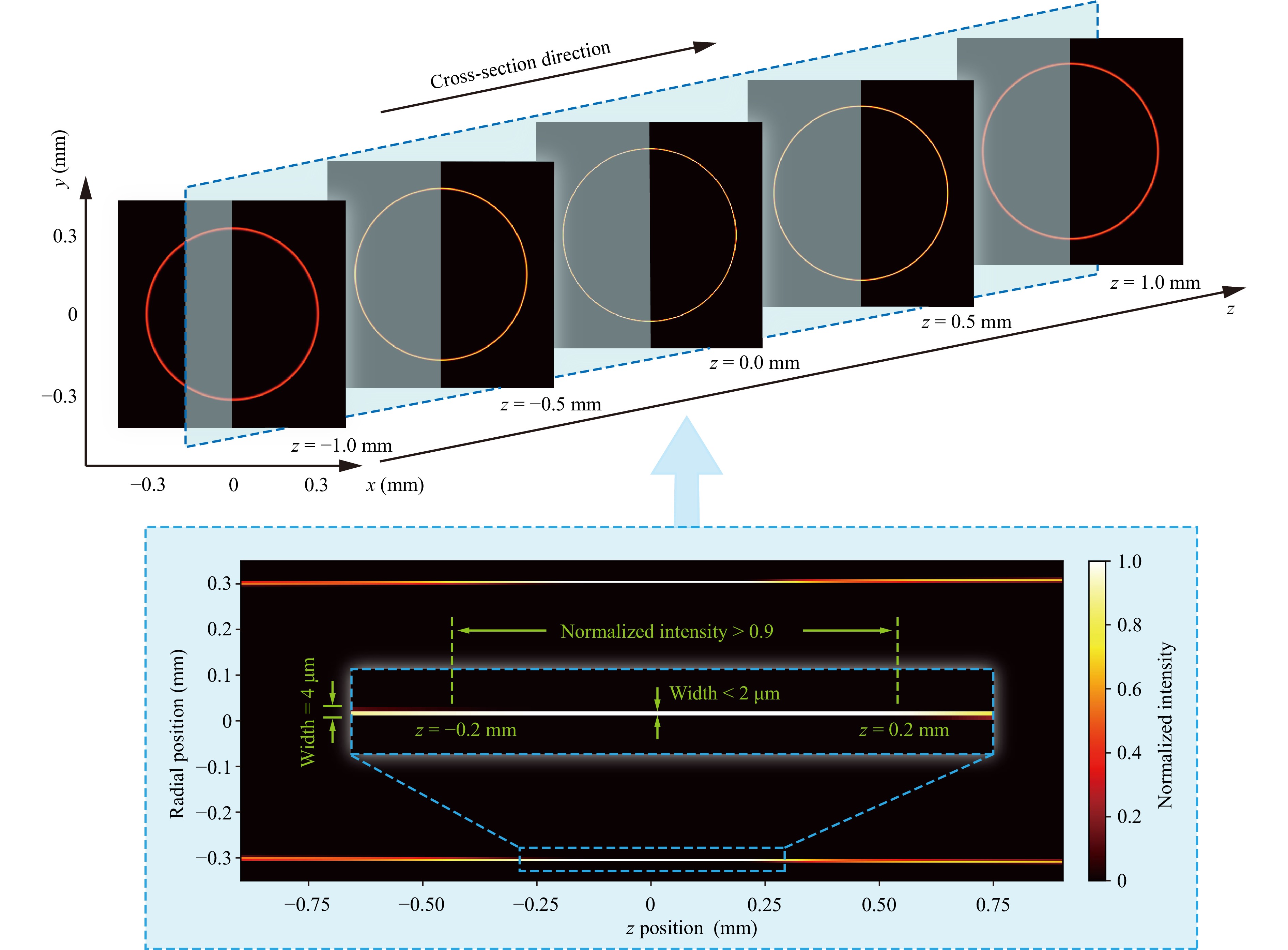
Fig. 2 Simulation of the intensity distribution. Cross-sectional images are captured in the x-y and radial planes. The image near the convergent area in the radial plane is magnified to illustrate intensity variations.
-
The experimental setup was constructed on a rubber-damped optical test platform, and the modulated ring-shaped patterns were captured using a camera. The experimental optical setup is shown in the Supplementary Information (Fig. S2) and details are provided in the Materials and Methods section.
As shown in Fig. 3a, b, the experimental setup was modified to produce ring-shaped patterns with diameters of approximately 800 and 400 µm. Cross-sectional data for both the horizontal and vertical orientations were collected to analyse the intensity distribution along the ring circumference. The data are plotted as line charts in Fig. S3 and S4. A slight offset was introduced during the plotting to differentiate between the horizontal and vertical intensity values, as indicated by the orange and blue lines, respectively. These profiles show that the beam has a high-intensity peak and a steep drop-off at its edge. Both orientations have similar diameters, demonstrating that the ring-shaped patterns exhibit good roundness. This feature will produce a clear, high-contrast exposure for lithographic applications.
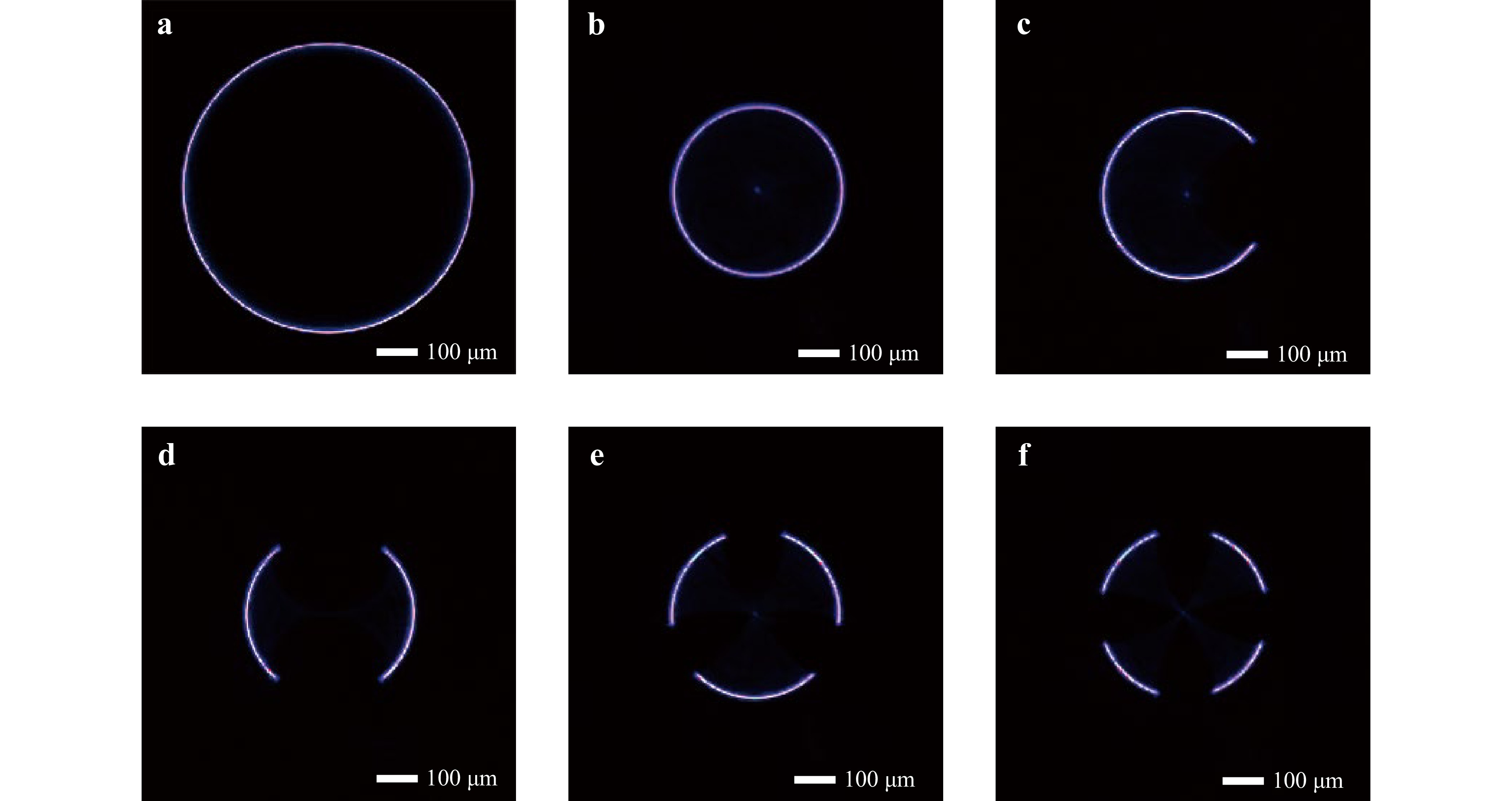
Fig. 3 Modulated ring-shaped patterns and their variations, captured by using a camera. Ring-shaped pattern with diameters of a 800 µm and b 400 µm. c-f Modulated split-ring patterns with one to four gaps.
Split-ring structures were generated by adding a small module and motorised blocking plates in front of the axicons. Various ring-like structures were formed at the image plane by controlling the shielded portions of the module. This optical–mechanical module functions similarly to a photomask in the optical setup. Gap orientations were adjusted by rotating the blocking plates. The examples in Fig. 3c-f display split-ring patterns with one to four gaps captured by a camera. Stray light near the blocked structures was minimal, with no impact on the lithography results. This feature diversifies the possible applications of the ACAL method to meet multiple requirements.
-
A photoresist-coated substrate was used to verify the ring width in the experimental setup. A fused silica substrate was spin-coated with a photoresist layer and fixed onto a substrate holder. After the exposure and wet process, the results with different diameters are coloured according to the photoresist surface height, as shown in Fig. 4a, c. Ring-shaped patterns with diameters of 800 and 400 µm were exposed using a pair of convex lenses (fLens1 = 500 mm and fLens2 = 20 mm). Patterns with diameters of 100, 50, and 24 µm were exposed using another pair of convex lenses (fLens1 = 500 mm and fLens2 = 8 mm). The ring width was measured at the ends of the four symmetry axes of each ring. The results are shown as line graphs in Fig. 4b, d. The average ring widths of the 800 and 400 µm ring-shaped patterns are 2.93 and 2.90 µm, with standard deviations of 0.12 and 0.10 µm, respectively. The average ring widths of the 100, 50, and 24 µm ring-shaped patterns are 1.99, 2.07, and 1.79 µm, respectively; their standard deviations are 0.21, 0.29, and 0.28 µm, respectively. These exposed ring-shaped patterns exhibit excellent symmetry, demonstrating that our optical setup is reliable for manufacturing finer and more variable ring-shaped patterns. Although the structural widths of the smaller ring-shaped patterns are less stable than those of the larger ones, the photoresist layer is still completely exposed. This experiment illustrates that our method is effective and has the potential to produce smaller ring patterns.
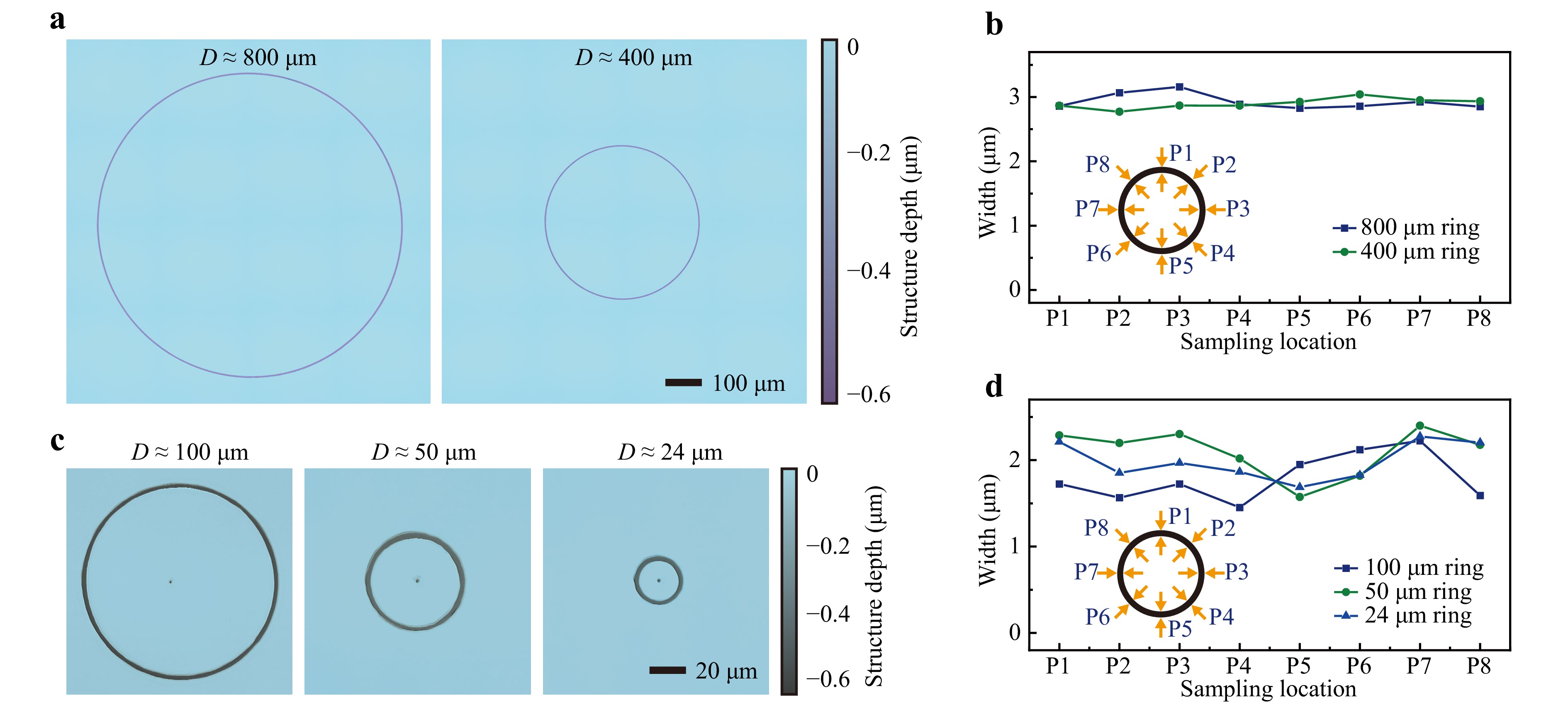
Fig. 4 Exposure experiments on a photoresist-coated planar substrate. a Ring-shaped patterns of 800 and 400 µm. b Graph illustrating the ring width at characterization locations for ring-shaped patterns of a. c Ring-shaped patterns of 100, 50, and 24 µm. d Graph illustrating the ring width at characterization locations for ring-shaped patterns of c.
-
Focal depth is a critical parameter in lithography as it determines the range for an objective, exposing qualified patterns. Generally, focal depth is inversely related to the numerical aperture of the imaging optical lens, calculated from the lens parameters67. However, this approach cannot be directly applied to our non-paraxial optical setup, which forms a hole annular beam. Therefore, a control experiment was conducted to assess the tolerance of the ACAL system, which can be considered the equivalent focal depth. Details of this experiment are described in the Materials and Methods section.
The ring width, which measures the left and right sides of each exposed ring-shaped pattern, is plotted as a scatter chart in Fig. 5b. Two evaluation criteria were used in this study. First, the exposed ring structure should completely penetrate the coated photoresist layer; otherwise, it was not considered further. Secondly, the deviation of the ring width should less than 30% from the target of 4 µm. The eligible areas are highlighted with a light-green background. Our ACAL setup produced five ring-shaped patterns that met both criteria, whereas the commercial DLWL system produced only three suitable patterns. Multiplying these numbers with the defocus interval (Δz) between each exposed unit, the eligible defocusing range of the ACAL setup and the DLWL system were 240 and 24 µm, respectively. This experiment indicates that the equivalent focal depth of our ACAL setup is ten times greater than that of the commercial DLWL system.
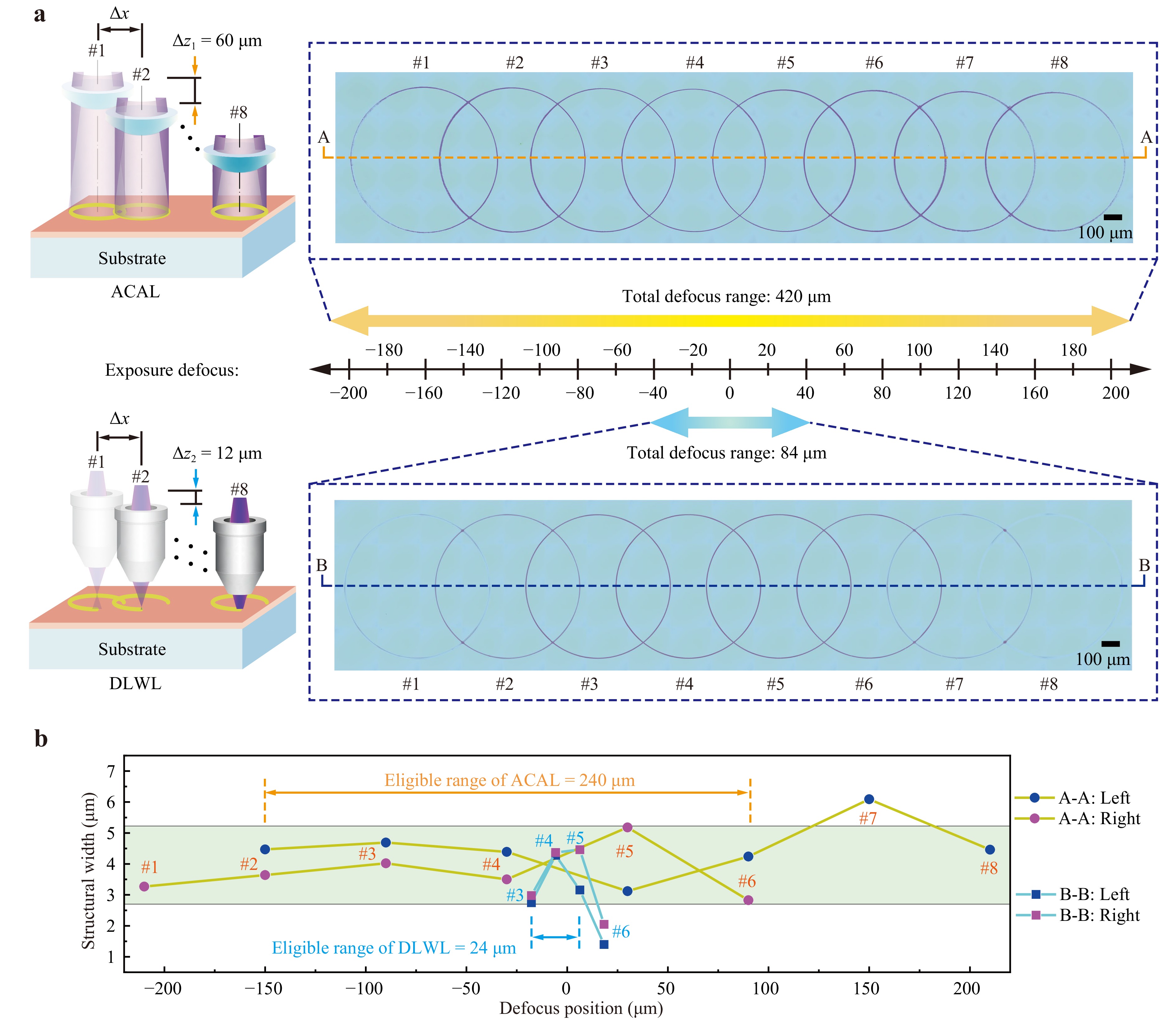
Fig. 5 Comparative experiment for the focusing depth of the ACAL and DLWL systems. a Exposure results of the ACAL and DLWL systems. Ring patterns are exposed with the same interval of Δx = 500 µm. Defocus intervals are Δz1 = 60 µm and Δz2 = 12 µm for the ACAL and DLWL systems, respectively. The cross-sectional ring width was measured along the horizontal direction of “A-A” and “B-B”, respectively. b A line chart illustrating the ring width of the above experiments. Each ring pattern is measured at its left and right sides. The eligible area (structural width fluctuation less than 30%) is coloured with a light-green background.
-
Although the aforementioned experiment verified the performance of the ACAL method, additional challenges may arise when exposing an actual curved surface. This experiment evaluated the exposure performance on a convex lens, which served as a curved substrate with a radius of 15.5 mm and a diameter of 20 mm. The experimental setup is shown in Fig. 6a. A series of positional errors were deliberately introduced into this experiment by shifting the exposure location without focusing. This led to beam defocusing, typically manifesting as an incomplete exposure of the photoresist layer. The sample on the right side of Fig. 6b, exposed to dozens times the standard laser power, exhibits the overall ring positions on the dome surface. Six white ring-shaped traces appear on the substrate surface, with shadows cast on the table. The sample on the left was exposed to the optimal dose, demonstrating the effectiveness of the ACAL method.
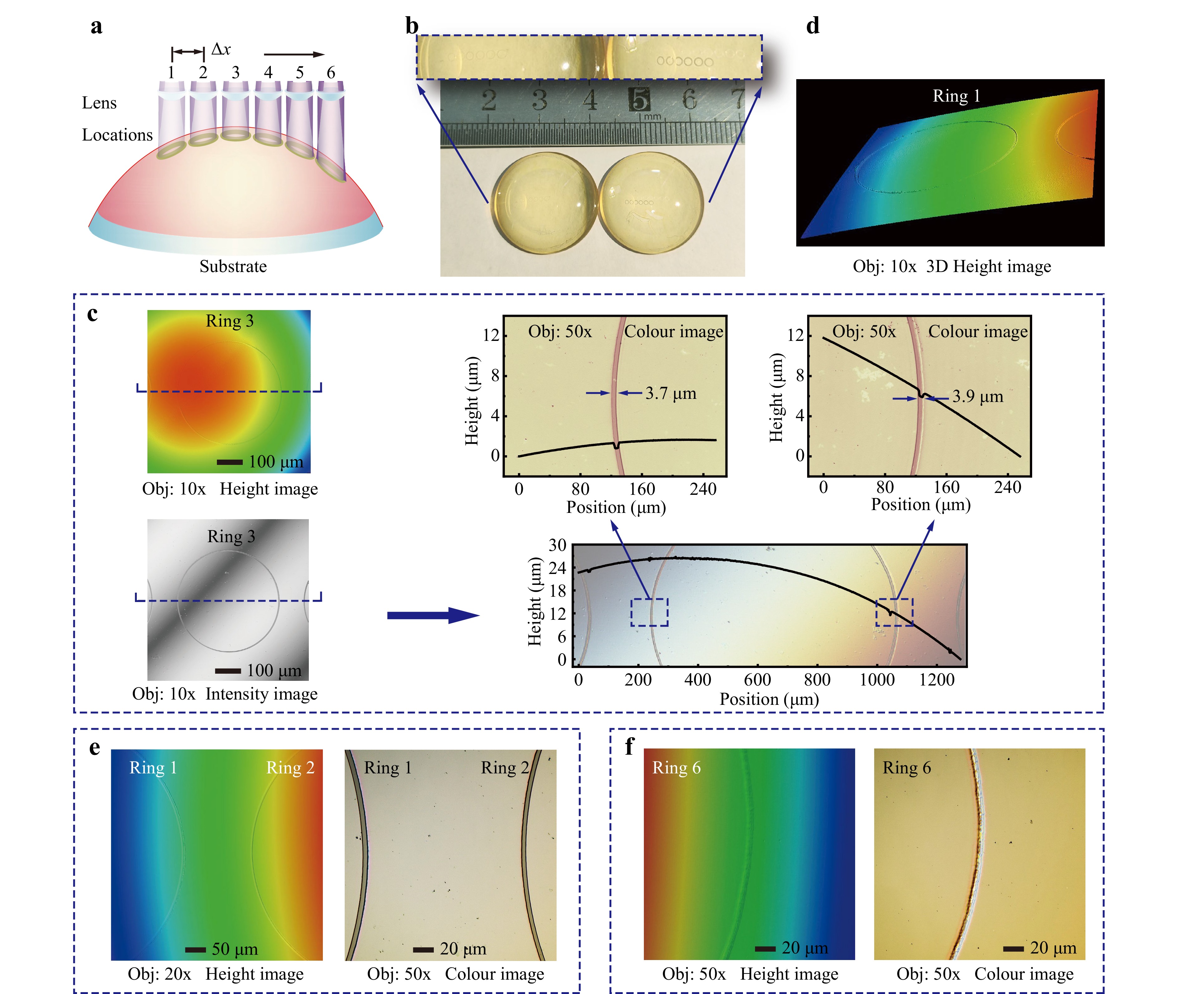
Fig. 6 Exposing ring-shaped patterns on a curved substrate. a Schematic of the exposure method, with horizontal shifts of Δx = 500 µm applied between each exposure. b The overall picture of the curved substrate. The overexposed sample on the right illustrates the exposure locations of units. The sample on the left was exposed to the optimal exposure dose, the patterns of which were captured and measured, as shown in Fig. 6c-f. c Images of the third ring pattern, captured in height and intensity modes. Line charts illustrate the cross-sectional data at each side of the ring structure. d 3D height image of the first ring-shaped pattern. e Height images of the first and the second ring structures. f Height images on the right side of the sixth ring pattern.
The third ring-shaped pattern, shown in Fig. 6c, is located closest to the focal position. This unit has only a slight horizontal misalignment, which resulted in a height variation of several micrometres between the left and right sides. This positional error is observed in the height image and line chart of the cross-sectional profile. Owing to the long focal depth, excellent exposure results are maintained. The measured structural widths differ by only 0.2 µm between the two sides of the ring-shaped pattern. These advantages were also evident at the other exposure locations. As shown in Fig. 6d, e, although the positional errors increase, the structures of the first and second ring-shaped patterns continue to penetrate the photoresist layer. Only the sixth ring-shaped pattern (Fig. 6f) exhibits poor structural quality due to the significant positional error. This experiment confirms the feasibility of the ACAL method for practical applications and demonstrates its effectiveness in producing high-quality ring-shaped patterns on curved surfaces.
-
This study introduces a novel approach to annular lithography that enables the manufacture of ring-shaped structures using lens aberration. These findings provide valuable insights into the fabrication of ring-shaped units on curved surfaces. However, the robustness of this novel lithography method for practical applications requires further investigation. Power fluctuations in the laser source are a common source of errors in structural quality variation. An experiment was conducted in which the exposure duration was adjusted to simulate the effect of laser fluctuations on the ring width. As shown in Fig. 7a, the exposure dose that produces a structural width of 3 μm was set as the ACAL system’s default parameter. This line chart clearly demonstrates that the average ring width is positively correlated with the exposure dose. On average, each percent variation in the exposure dose results in a 0.74% increase in the ring width. The standard deviation of structural width increases when the average structural width decreases to less than 3 μm. This indicates that the structural width is unstable under these conditions. Therefore, maintaining a stable laser source intensity and an appropriate level of overexposure are beneficial for improving structural quality. Defocusing error is another common factor that results in poor lithography results. Fig. 7b shows the effect of defocusing error on the structural width. It is evident that ring width changes only slightly, despite defocusing errors occurring at each exposure dose level. This test demonstrates that the ACAL system is sufficiently reliable to avoid fluctuations in defocusing.
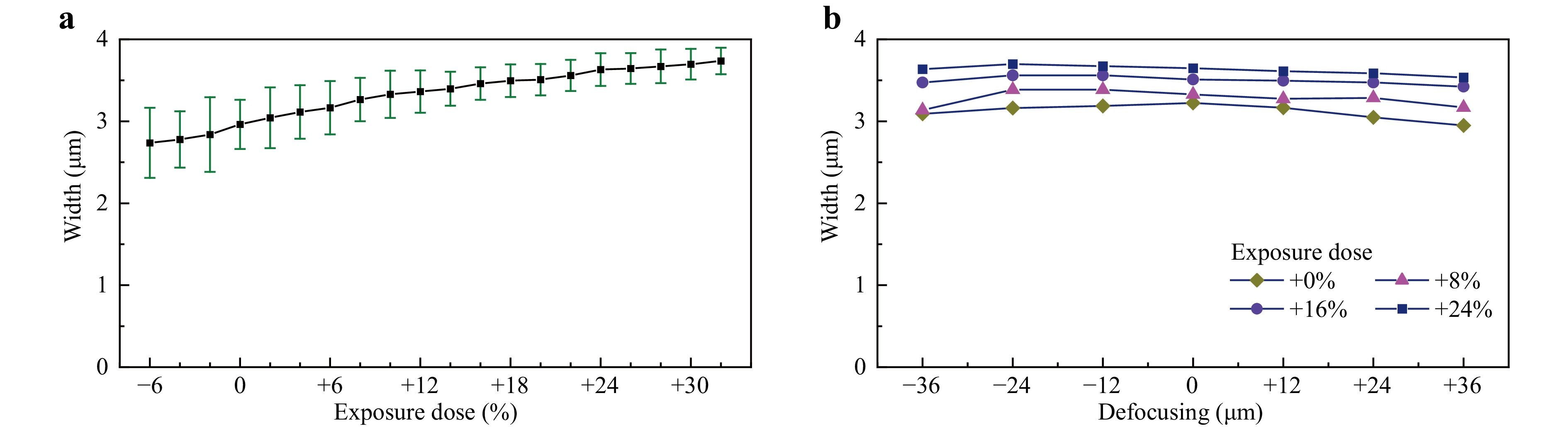
Fig. 7 Robustness tests for the ACAL system. a Effect of the exposure dose on the ring width. b Effect of the defocusing errors on the ring width.
Table 1 summarises recent annular lithography studies that did not use microscope objectives to miniaturise the beam. Our work significantly improves the performance of annular lithography in terms of two key parameters: minimum structural size and diameter variation. Additionally, in contrast to the previous studies, we verified that our ACAL method is applicable to curved surfaces. Nevertheless, expected challenges exist during the exposure of curved substrates, such as requiring 3D autofocus systems and maintaining photoresist coating uniformity. Despite these challenges, the results are only slightly worse than those for the flat substrates.
Published year Research institution Minimum ring width (μm) Ring diameter range (mm) Test-based substrate 202263 University of Applied Sciences Jena, Germany 75 1.6-6.2 Flat 202364 University of Applied Sciences Jena, Germany 18.8 1.8-3.7 Flat This work Harbin Institute of Technology 1.79 (3.7 on curved surface) 0.024-0.8 Flat & Curved Table 1. Recent annular lithography studies
Depending on the ACAL method, each pair of convex lenses corresponds to a specific range of diameter adjustments. Replacing different pairs of convex lenses allows the diameter to be adjusted to other ranges. As shown in Fig. 4, the ring-shaped patterns exposed with fLens2 = 8 mm have narrower structural widths than those exposed with fLens2 = 20 mm. This phenomenon occurs because the convex lens group also plays a role in reducing the beam size, similar to a telescope, while converging the beam layers. To obtain a large ring-shaped pattern with a narrow ring width, it is useful to replace Lens1 with one of larger diameter and use a short-focus Lens2. Additionally, it should be noted that the ring-shaped pattern exposed with fLens2 = 8 mm is rougher at the edges than that exposed with fLens2 = 20 mm. This issue arises from the poor performance of Lens2, which was purchased from a commercial market. This lens lacks sufficient quality with respect to surface topography and uniformity. The ACAL method imposes higher requirements on the convex lenses and their position adjustments when exposing smaller ring-shaped patterns.
DLWL systems have advantages for conventional planar substrate lithography. For instance, they can expose narrower structural widths and use exposure strategies, such as digital scanning and spatial light modulators, to increase the writing speed. However, extending these advantages to curved-surface lithography is difficult. Table 2 compares our method with DLWL methods for curved surface exposure with incomplete data referring to the specifications of the common products. Because the microscope objective is designed to image a planar surface, it cannot focus simultaneously on the centre and edge of a curved surface. Consequently, conventional DLWL methods must limit the exposed area and reduce their speed to allow for the autofocusing process. Certain applications rely entirely on pixel-by-pixel mechanical scanning. Furthermore, microscope objectives usually have limited focal depth. Maintaining a consistent distance and angle is challenging when a mechanical system drives the objective to scan each exposure position on a surface with a large curvature. Consequently, conventional approaches must choose between minimum structural width and structural quality56–58. These disadvantages render the manufacturing process inefficient and yield coarse outcomes despite the additional costs of advanced optical elements and high-precision microscope objectives. The ACAL system has the potential to overcome these challenges. This system can expose a complete ring-shaped pattern in a single exposure. It can enable the exposure of large-diameter rings with sizes that are usually larger than the field of view of an objective. It also has a greater equivalent focal depth. This feature enables the system to adapt to mechanical positioning errors that accumulate with multiaxis movements, allowing for higher-speed exposure and reducing the need for highly precise production machinery.
Focal depth Working distance Minimum structural width Exposure speed Cost ACAL 10 times larger than DLWL Longer, 31 mm
in this work3.7 μm on the tested dome Fast, impulse exposure Economic Conventional DLWL Shorter, less than 10 μm mostly67 Most objectives shorter than 17 mm68 Depend on substrate56–58 Slow, objectives limitations Expensive Table 2. Comparison of ring-shaped pattern exposure on curved surfaces
Although the working distance may not be crucial for planar lithography, it is important for curved surfaces. Commonly used microscope objective models have a working distance of less than 17 mm, and the experimentally compared DLWL system has a working distance of only 4.5 mm. In contrast, our ACAL setup has a working distance exceeding 30 mm. A longer working distance helps prevent spatial conflicts between steep-angled substrates and the lithography system during exposure, particularly when creating patterns on substrates with varying curvatures and scales. In addition, this feature provides more space for incorporating complex modules within the lithography system.
The concept of converging a beam through lens distortion can be utilised to expose a wider variety of shapes. For instance, special lenses can shape the beam into an ellipse or square and then refine it using lens aberration. Additionally, freeform or other aspherical optical elements can create finer structures by converging the beam simultaneously, rather than layer-by-layer (as shown in Fig. S1). However, this resulted in a discontinuous variation in diameter. Therefore, the approach is more suitable for fabricating products with fixed diameters.
Using this technology, electromagnetic shielding of metallic mesh grids, absorbers, stealth cloaks, and other metasurface elements on curved surfaces can be produced more easily. Its wide range of diameter adjustments makes this method applicable to other fields of study. A longer focal depth is useful for additive manufacturing, multiphoton lithography, and ultrafast laser material processing. By changing the laser source and integrating it with other lithography techniques, tiny units of hollow and columnar shapes can be rapidly produced.
In conclusion, this study provides a novel approach for annular lithography using lens distortion to modulate beams. The experiments show that the optical setup demonstrated significant advantages, achieving a ring width of 1.79 µm and adjustable ring diameters from 24 to 800 µm. The structure can be modified to expose split-ring patterns by adding blocking plates, and the diameter range can be adjusted by moving the lens position and switching the convex lens pairs. In addition, the optical setup offers a long equivalent focal depth and working distance. These remarkable characteristics facilitate annular lithography on curved surfaces, addressing complex issues related to positional errors and surface-height variations within the extended focal depth. Our ACAL method delivers high-resolution exposure of 3.7 µm ring-shaped structures on a 15.5 mm radius dome substrate, which is a performance not previously achieved using annular lithography. This creative technology is promising for applications such as metasurfaces.
-
The choice of lens pairs determines the adjustment range of the ring diameter. In our experimental setup, Lens1 had a focal length of 500 mm and a diameter of 25.4 mm, while Lens2 was used in two configurations. The first and second configurations had focal lengths of 20 and 8 mm, respectively. Both configurations had a Lens2 diameter of 6 mm. The axicons each had a wedge angle of α = 10°. The lens distance parameters for the simulation and experimental setups were calculated using Eqs. 2, 3. The 405 nm fibre-coupled UV laser diode, with a typical output power of 80 mW, along with the fibre and collimator were supplied by the laser manufacturer.
The annular beam image was captured using a camera (HIKROBOT MV-CS050) mounted on a substrate holder to record the intensity distribution in the image plane. In additional experiments, a positive photoresist (Merck KGaA AZ1505) approximately 0.48 µm thick was spin-coated onto a planar or dome-shaped substrate. The spin speed was set to 4000 rpm, and a pre-bake temperature of 100 °C for 60 s was applied. During the exposure dose tuning, the fibre laser diode output was set to the lowest frequency using a pulse-width modulation controller, yielding a power of 0.31 mW. The exposure duration was varied by adjusting the on/off state of the shutter. A 2.5% attenuation plate was integrated into the optical setup. Exposure durations were set to 900, 800, 570, 430, and 260 ms for ring patterns of diameters 800, 400, 100, 50, and 24 µm respectively. For the defocus experiments, the exposure was extended to 1100 ms to achieve a ring width of 4 µm.
The experiment to determine equivalent focal depth was performed on a planar substrate coated with photoresist. A set of ring patterns was exposed in our experimental setup, as shown in the upper row of Fig. 5a. For comparison, another row of patterns was produced using a commercial DLWL system (Heidelberg Instruments, DWL66+). This general-purpose system was designed to produce binary and greyscale structures on flat surfaces. We selected Write Mode III for our comparison in the Results and Discussion sections to fabricate a ring-shaped pattern with smooth edges69. This mode uses a Nikon TU Plan Fluor 20× objective with a working distance of 4.5 mm and a numerical aperture of 0.45. Although Write Mode IV and V have longer working distances, they often result in rough edges on curved structures and it can be difficult to fabricate such thin structures. During the experiments, the autofocus function was fixed to prevent defocusing adjustments at each exposure position. Our ACAL system was configured to produce ring patterns with a diameter of 800 µm and ring width of 4 µm by adjusting the exposure dose at the optimal defocus position. The control group was assigned similar ring-shaped patterns. In each group, eight overlapping ring-shaped units were exposed at a fixed horizontal interval (Δx = 500 µm). However, their exposure positions were shifted vertically at different intervals around the ideal focal position of the objective. For our setup, Δz1 was set to 60 µm; however, for the control group, Δz2 was 12 µm because of its limited focal depth.
The experiments on the curved substrate, shown in Fig. 6, exposed six ring patterns on the surface of a convex lens. Convex lenses coated with photoresist served as dome-shaped substrates. The ACAL system was maintained at a constant distance from the substrate holder while shifting horizontally to each exposure location. Only the surface area at the third ring was aligned with the image plane, whereas the other rings remained slightly out of focus. Consequently, the vertical distances between the centre of each ring-shaped pattern and the image plane were 129.6, 32.3, 0, 32.3, 129.6, and 293.1 µm.
After exposure, the samples were developed using wet processing. The samples were immersed in a 1:4 dilution of Merck AZ400k developer for 30 s, rinsed with deionised water, and dried with compressed air.
The topography of the exposed surfaces was characterised using a laser confocal scanning microscope (OLYMPUS, OLS5100). As illustrated in Fig. S5, the characteristic ring width refers to the width near the base of the photoresist layer. This standard measurement was used in other lithography studies63 was used to assess the subsequent processes. For planar substrate testing, the height data were stitched together using software. For curved substrates, profile results were captured at each location to avoid physical interference and loss of critical height data during stitching.
-
This study was supported by the National Natural Science Foundation of China (NSFC) under Grant Nos. 61975046 and 62575090.
Ultra-long focal depth annular lithography for fabricating micro ring-shaped metasurface unit cells on highly curved substrates
- Light: Advanced Manufacturing , Article number: (2025)
- Received: 05 December 2024
- Revised: 30 June 2025
- Accepted: 03 July 2025 Published online: 12 October 2025
doi: https://doi.org/10.37188/lam.2025.056
Abstract: In recent years, metasurfaces on planar substrates have been extensively investigated and methods for their fabrication have been implemented. However, fabricating metasurfaces on highly curved surfaces remains challenging because of the difficulty in achieving precise mechanical positioning on curved geometries using current lithographic techniques. This limits applications that require finer and more accurate structures. This paper introduces a novel lithographic approach for patterning structures on curved surfaces. By leveraging the natural aberration of a convex lens to focus the beams, this approach enables the creation of adjustable ring and split-ring configurations. Ring-shaped patterns with an average structural width of 1.79 µm were exposed, exceeding the resolution of previously reported annular lithography techniques by a factor of 10. Moreover, this approach offers a defocus tolerance that is 10 times greater than that of conventional direct laser writing lithography, thus reducing the influence of positional errors caused by substrate geometry. Consequently, patterns on a photoresist-coated dome were successfully exposed, marking a pioneering achievement. This study paves the way for creating ring-shaped metasurfaces and other structures on highly curved surfaces.
Rights and permissions
Open Access This article is licensed under a Creative Commons Attribution 4.0 International License, which permits use, sharing, adaptation, distribution and reproduction in any medium or format, as long as you give appropriate credit to the original author(s) and the source, provide a link to the Creative Commons license, and indicate if changes were made. The images or other third party material in this article are included in the article′s Creative Commons license, unless indicated otherwise in a credit line to the material. If material is not included in the article′s Creative Commons license and your intended use is not permitted by statutory regulation or exceeds the permitted use, you will need to obtain permission directly from the copyright holder. To view a copy of this license, visit http://creativecommons.org/licenses/by/4.0/.

 DownLoad: