


-
Metal nanoparticles (NPs) supporting localized surface plasmon resonances offer new possibilities for manipulating light-matter interactions at the deep-sub-wavelength scale. A single NP usually suffers from plasmonic losses. By comparison, NPs arranged into an array (e.g., a one-dimensional (1D) NP chain) or/and a hybrid plasmonic-photonic structure (e.g., NPs on microfibres) can significantly engineer plasmonic resonances with stronger enhancements and sharper linewidths. This enables various novel phenomena such as high-quality lattice plasmon resonance1,2, intense optical scattering3,4, enhanced nonlinear effects5,6, and deep-subwavelength waveguiding7–11, which offer new opportunities for numerous applications including plasmonic sensing12–15, surface-enhanced Raman scattering (SERS)16–18, enhanced molecular imaging19,20, and plasmonic nanolasing21.
Therefore, the ability to manipulate metal NPs into well-defined patterns is crucial for fundamental research and technological applications15,22,23. Various template-assisted and template-free approaches have been developed to fabricate high-quality plasmonic arrays. Although the former approaches exhibit high throughput (e.g., nanosphere lithography24,25, nanoimprint lithography26–28, and PEEL29,30 (i.e., a combination of phase-shifting photolithography, etching, electron-beam deposition, and lift-off of the film)), the latter approaches eliminate the requirement of a high-resolution template and exhibit high morphological tunability. However, conventional template-free approaches use electrons31,32 or focused ion beams33 for direct writing, which limits their applications due to complex procedures, high operational costs, vacuum requirement, and possible sample contamination by the implanted electrons/ions.
To circumvent these issues, ultrafast laser writing has emerged as a competitive alternative owing to simple, cost-effective, vacuum-free, and non-polluting processing34,35. However, because ultrafast laser writing is an optical approach, the achievable dimension limit is strongly related to the confinement capability of light; therefore, it encounters the well-known challenge of diffraction limit. To reach the nanoscale, common strategies, such as ultrashort-wavelength lasers, nonlinear effects triggered by ultrashort pulses, and super-resolution focusing, usually require sophisticated equipment (extreme ultraviolet or femtosecond lasers), specific materials for nonlinear interaction, and complex designs for focal engineering (e.g., superlenses)34,36. Moreover, most of these methods are direct-focusing approaches, which face challenges in terms of the fabrication speed as a serial process. Alternatively, laser interference writing37,38, which is based on multi-beam interference to form a periodic pattern, offers a high-throughput parallel fabrication process; however, its beam alignment can be time-consuming and complex39.
In this study, under a single exposure to a loosely focused nanosecond laser beam, we generated 1D plasmonic arrays by leveraging the self-organized patterns of tightly confined surface plasmon polaritons (SPPs) (Fig. 1). Based on both simulations and experiments, we systematically investigated and elucidated that the light-driven mechanism involves two processes: (1) generation of a self-redistributed electromagnetic field pattern under the synergistic effect of a standing wave and optical beating and (2) formation of periodic geometries regulated by a spatially modulated temperature distribution. For experimental demonstration, high-quality 1D Ag NP arrays featuring optimized unit structures and lattice geometries with supra- or sub-wavelength periods beyond the diffraction limit were fabricated from single Ag nanowires (NWs). The developed approach exhibited high tunability in terms of the NP size, interparticle spacing, and alignment direction. More importantly, we showed that the developed method can be used to fabricate plasmonic arrays directly on a curved substrate or microstructure. As a conceptual proof, Ag NP arrays were fabricated on freestanding microfibres (with diameters down to ~1.4 µm) along the fibre axis, thereby forming a series of hybrid plasmonic-photonic microcavities with narrow-band resonances (~3.9 nm linewidth) as well as a barcode system with high multiplexing capacity. This approach provides a simple, low-cost, and high-efficiency method for manufacturing periodically aligned plasmonic nanostructures on various substrates (especially on non-conducting and curved surfaces), thereby paving the way towards nanoscale lasing, enhanced SERS, information encryption, and high-resolution distributed sensing.
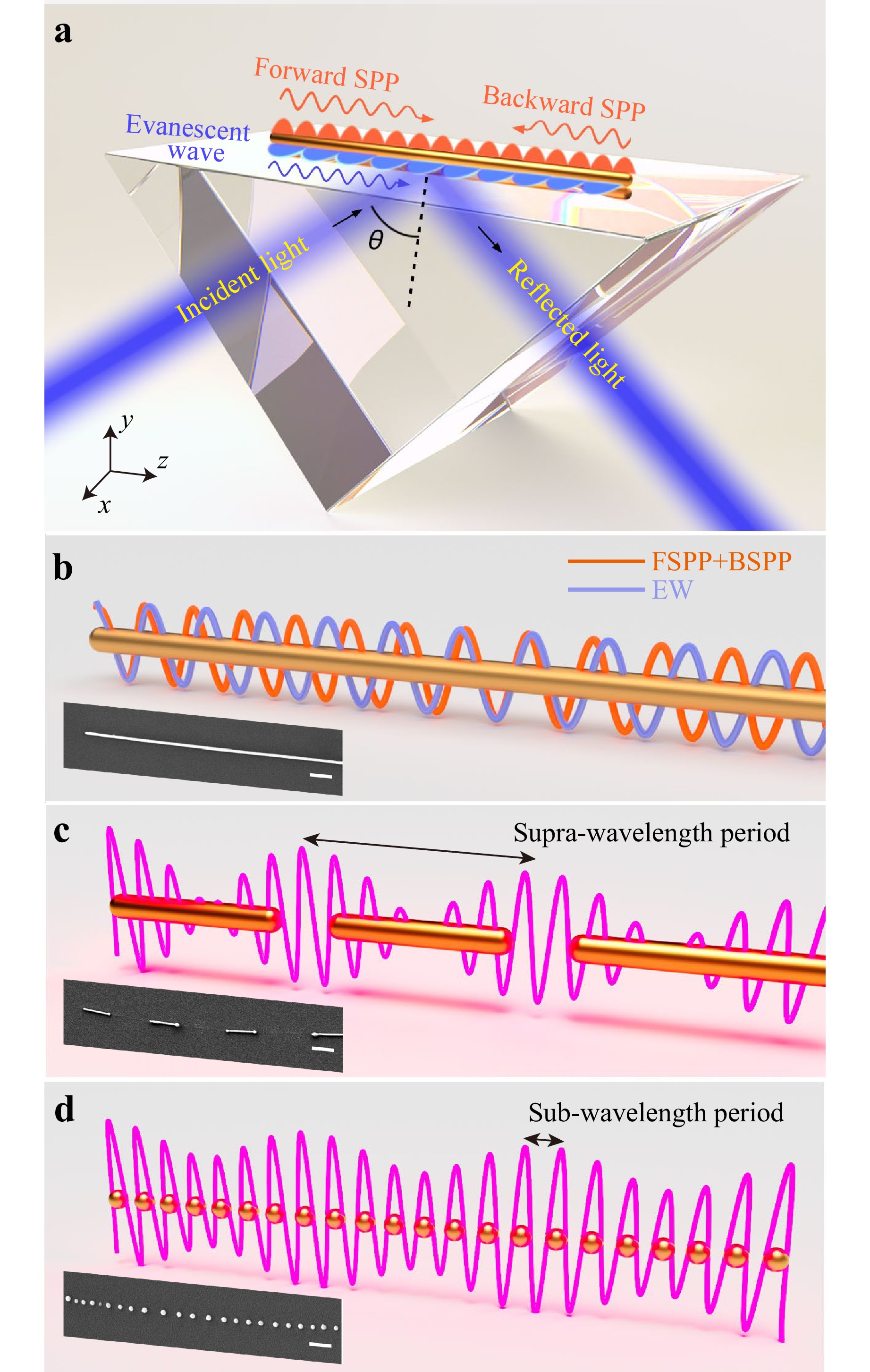
Fig. 1 Schematics of generating 1D plasmonic arrays by leveraging light-driven self-organization. a configuration of a metal NW system supporting multiple waves to generate a periodic electric field distribution. Under illumination of an obliquely incident laser beam, SPPs are excited at the left end-facet and propagate forward, which are called as forward SPPs (FSPPs). The FSPPs travel to the right end-facet and are reflected, causing them to travel backward; these SPPs are named as backward SPPs (BSPPs). Evanescent waves (EWs) also exist at the interface. b illustration of the superposition of FSPPs, BSPPs, and EWs on a NW, which results in a standing-wave or beating effect to form periodic electric fields. Inset scalebar, 500 nm. c formation of metal nanostructure arrays with supra-wavelength periods regulated by spatially modulated |E| distribution. Inset scalebar, 1 μm. d formation of metal nanostructure arrays with sub-wavelength periods. Inset scalebar, 500 nm.
-
As shown in Fig. 1a, we first define propagating waves in our developed scheme. Excited by the obliquely incident light at the left end of a Ag NW, the SPP mode propagates forward to the right end (forward SPP, FSPP), whose electric field components are expressed as40
$$ E_{y,{\textit z}}^{{\text{FSPP}}} = {( - {\text{i}})^{0,1}}AE_{y,{\textit z}}^{{\text{sp}}}\exp ( - \alpha {\textit z})\exp [{\text{i}}({k_{{\text{sp}}}}z - \omega t + {\varphi _{{\text{sp}}}})] $$ (1) where A is the amplitude, ksp = k0neff = 2πneff/λ is the propagation constant of the plasmon, neff is the effective refractive index, λ is the wavelength of light, α denotes the plasmon mode attenuation, c is the speed of light, ω is the angular frequency of light, φsp is the initial phase, and $ E_{y,{\textit z}}^{{\text{sp}}} $ denotes for the transverse field distribution for the y- or z-component of the electric field, respectively. For simplicity, the field component Ex, which has a form similar to Ey, is omitted.
When the FSPP travels to the right end, it is reflected, thereby producing a backward SPP (BSPP), which can be written as41,42
$$\begin{split} {E}_{y,{\textit z}}^{\text{BSPP}}=\;&{(-\text{i})}^{0,1}Ar{E}_{y,{\textit z}}^{\text{sp}}\mathrm{exp}[\alpha ({\textit z}-2L)]\\&\mathrm{exp}\{-\text{i}[{k}_{\text{sp}}({\textit z}-2L)+\omega t-{\phi }_{\text{sp}}-\delta ]\} \end{split}$$ (2) where L and reiδ are the NW length and complex reflection coefficient of the endface, respectively.
In a typical silica prism excitation setup, another propagating wave is the evanescent wave (EW), which results from the total internal reflection at the air-silica interface. To launch the fundamental mode, which is favourable in most applications43, a p-polarized incident light is typically used, whose corresponding EW components are expressed as44
$$ \begin{gathered} E_{y,{\textit z}}^{{\text{EW}}} = {( - {\text{i}})^{0,1}}B{\eta _{y,{\textit z}}}\exp ( - {k_ \bot }y)\exp [{\text{i}}({k_\parallel }{\textit z} - \omega t + {\varphi _{y,{\textit z}}})] \\ {k_\parallel } = {k_0}{n_{\text{s}}}\sin \theta ,{k_ \bot } = {k_0}\sqrt {{{({n_{\text{s}}}\sin \theta )}^2} - n_{\text{a}}^2} \end{gathered} $$ (3) where B is the field amplitude of the wave, θ is the incident angle satisfying the total internal reflection (sinθ > na/ns), ns and na are the refractive index of the prism and air, respectively, and complex quantities ηyeiφy and ηzeiφz denote the combined efficiency factors accounting for the efficiency of Fresnel transmission and polarization in metals, respectively.
-
The superposition of the propagating waves described above (FSPP, BSPP, and EW) results in steady-state field patterns, which create periodic temperature distributions along the NW for further fabrication of plasmonic arrays (Fig. 1b-d), which can be expressed as follows:
$$ E_{}^{{\text{tot}}} = E_{}^{{\text{FSPP}}} + E_{}^{{\text{BSPP}}} + E_{}^{{\text{EW}}} $$ (4) Depending on the travelling direction and wavenumber, two types of superpositions exist: beats and standing waves. For a long NW (e.g., when the NW length is similar to or larger than the propagation length of the SPP), owing to the propagation loss, the BSPP is relatively weak and can be neglected compared with the FSPP and EW. Therefore, we consider the superposed wave as the summation of the FSPP and EW mainly, which should consist a superposition term of the two waves with the same amplitude components as follows:
$${ \begin{split}& E_{y,{\textit z}}^{{\text{sum}}1} \propto \exp [{\text{i}}({k_{{\text{sp}}}}{\textit z} - \omega t + {\varphi _{{\text{sp}}}})] + \exp [{\text{i}}({k_\parallel }{\textit z} - \omega t + {\varphi _{y,{\textit z}}})] \\ =\;& 2\cos \left(\frac{{{k_{{\text{sp}}}} - {k_\parallel }}}{2}{\textit z} + \frac{{{\varphi _{{\text{sp}}}} - {\varphi _{y,{\textit z}}}}}{2}\right)\exp \left[{\text{i}}\left(\frac{{{k_{{\text{sp}}}} + {k_\parallel }}}{2}{\textit z} - \omega t + \frac{{{\varphi _{{\text{sp}}}} + {\varphi _{y,{\textit z}}}}}{2}\right)\right] \end{split} }$$ (5) which results in beats with a supra-wavelength period Λ1 = 2π/(ksp − k||) = 2λ/(neff − nssinθ) that dominates (Fig. 1c). Note that, although φy and φz may be different, the periodic pattern still holds owing to a very small difference (i.e., |φy − φz| < 1.1 see Supplementary Information).
For a short NW, the BSPP becomes appreciable. To simplify the analytical study of field periodicity, we neglected the attenuation of plasmons (α = 0) and assumed the magnitude of the reflection coefficient as r = 140. The interference of the FSPP and BSPP can be expressed as
$$ {\begin{split}&{E}_{y,{\textit z}}^{\text{sum}2}\propto \mathrm{exp}[\text{i}({k}_{\text{sp}}{\textit z}-\omega t+{\varphi }_{\text{sp}})]+\mathrm{exp}\left\{-\text{i}[{k}_{\text{sp}}({\textit z}-2L)+\omega t-{\varphi }_{\text{sp}}-\delta ]\right\}\\ =\;&2\mathrm{cos}[{k}_{\text{sp}}({\textit z}-L)-\delta /2]\mathrm{exp}[\text{i}({k}_{\text{sp}}L-\omega t+{\varphi }_{\text{sp}}+\delta /2)]\end{split} }$$ (6) which forms a standing-wave pattern with a sub-wavelength period Λ2 = 2π/ksp = λ/ neff (Fig. 1d). Note that the amplitudes of the BSPP are much smaller than those of the EW, thereby leading to a negligible interference pattern, which was verified by numerical simulation.
-
To validate our theory, an electromagnetic scattering study was conducted using the finite element method (FEM) in COMSOL Multiphysics. As shown in Fig. 2a, periodic electric field patterns are naturally formed on the Ag NWs under plane-wave excitation. The patterns obtained from the numerical simulations are in good agreement with those fitted using Eq. 4. This verifies the effectiveness of the simulation and analytical models. The evolution of the field patterns with the NW length varying from 1 μm to 8 μm is also presented in Fig. 2a, b. Noticeably, the sub-wavelength period Λ2 and supra-wavelength period Λ1 dominate in short (e.g., L = 1, 2 μm, Fig. 2a, b(i-ii)) and long (e.g., L = 4, 8 μm, Fig. 2a(iii-iv)) NWs, respectively, which is in agreement with the prediction of our analytical model.
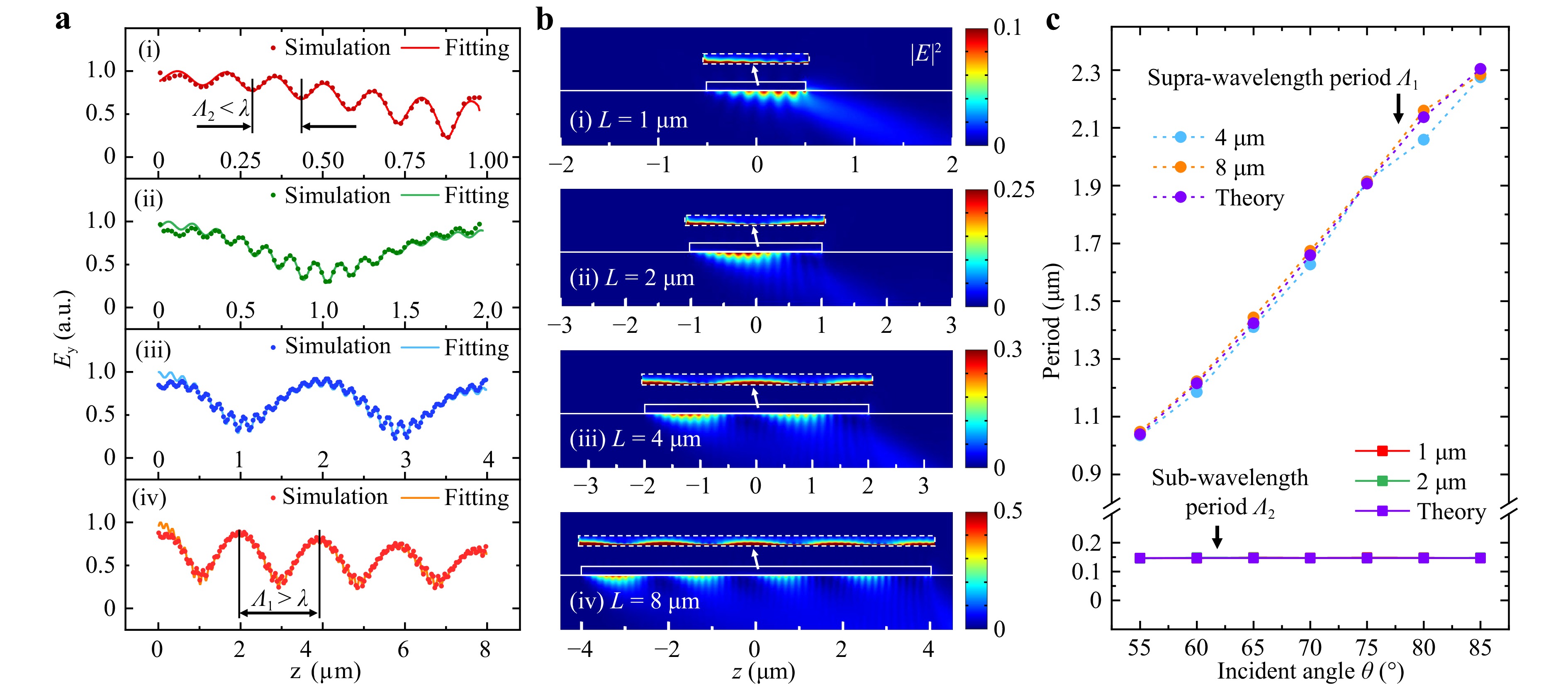
Fig. 2 Periodic electrical field patterns in a self-redistributed behaviour. a calculated (curves) and simulated (dots) electric field norm |E| inside 90-nm-diameter Ag NWs with lengths L = 1 (i), 2 (ii), 4 (iii), 8 μm (iv) at 490-nm-wavelength for y = 5 nm (y = 0 indicates the bottom line of the NW), and θ = 75°. b simulated normalized electric field intensity (|E|2) distribution for L = 1 (i), 2 (ii), 4 (iii), and 8 μm (iv), respectively. For better clarification, insets plot the |E|2 distribution inside the NWs with the colour bar ranging from 0 to 0.025 with saturation. c sub- and supra-wavelength periods versus the incident angle of the laser beam for different NW lengths.
We further investigated the dependence of the above two types of periods on the incident angle θ variation. As shown in Fig. 2c, the supra-wavelength period Λ1 measured from the field patterns (purple dotted-dashed line) agrees well with the theoretical values obtained from Eq. 5 (blue and orange dotted-dashed lines). It exhibits a large tunable range from 1000 to 2200 nm as θ changes from 55° to 85°. The sub-wavelength period Λ2 has a constant value of ~147 nm, which is independent of the angle θ. Λ2 can be tuned by adjusting the irradiation laser wavelengths or the effective refractive index, which is related to the NW diameter and surrounding, as indicated by Λ2 = λ/neff in the theoretical model (Eq. 6). The two types of periods for different NW lengths, along with their two distinct relationships to the incident light, can be used to form different periodic temperature distributions and generate plasmonic arrays with tunable interparticle spacings.
-
To characterize the photothermal effects caused by the periodic electric fields, we described the material response using a transient heat transfer model45–47. Because the electron-lattice thermal equilibration for metals (~5 ps48) is much shorter than the laser pulse duration (~2 ns in our case), the electrons and lattice were considered to have a common temperature T. The model equation is as follows:
$$ {C}_{\text{s}}\rho \frac{\partial T}{\partial t}+\nabla \cdot(-k\nabla T)={Q}_{\text{s}} $$ (7) where T is the time- and space-dependent temperature and Cs, ρ, k, and Qs are the heat capacity, density, thermal conductivity, and heat source per unit volume, respectively. The k value is crucial in solving this equation. For metal nanostructures, scattering from the grain boundary and surface is significant, which drastically changes the electron mean free path and subsequently reduces the thermal conductivities49–52. Previous studies have shown that the thermal conductivity k of a 147-nm-diameter Ag NW is 64.8 W K−1 m−1)51, which is only 15% of the bulk Ag. Using the Lu model49 and including the Kapitza resistance term52, the thermal conductivity k of the 90-nm-diameter Ag NW used in our model was determined as 42.3 W K−1 m−1 (see Supplementary Information). Owing to the lossy nature of the metal, the resistive heat Qs generated in the NW can be calculated as follows:
$$ {Q_{\text{s}}} = \frac{1}{2}{\varepsilon _0}\omega {\rm Im} ({\varepsilon _{\text{r}}}){\left| E \right|^2} $$ (8) where ε0 is the vacuum permittivity, εr is the relative permittivity of the metal, and E is the electric field. Therefore, the time-dependent temperature distribution can be obtained by numerically solving Eq. 6 using the FEM implemented in COMSOL Multiphysics.
The temperature distributions for NWs with L = 1, 2, 4, and 8 μm and their close-up views are presented in Fig. 3a, b, respectively. The results show that for the NWs with L ≥ 4 μm, the temperature distributions exhibit a dominating supra-wavelength period (Λ1 ≈ 1900 nm), whereas the sub-wavelength period becomes almost invisible owing to the fast heat conduction of the metal (Fig. 3a, b(iii–iv)). Only for extremely short NWs (e.g., L = 1, 2 μm, Fig. 3a, b(i–ii)), the sub-wavelength period appears. Note that, this does not mean that only an NW with L < 2 μm can produce sub-wavelength-period NP arrays. In fact, a long NW can first break into short fragments with supra-wavelength periods, with each of the short fragments serving as a short NW and being ablated into particles with sub-wavelength spacing.
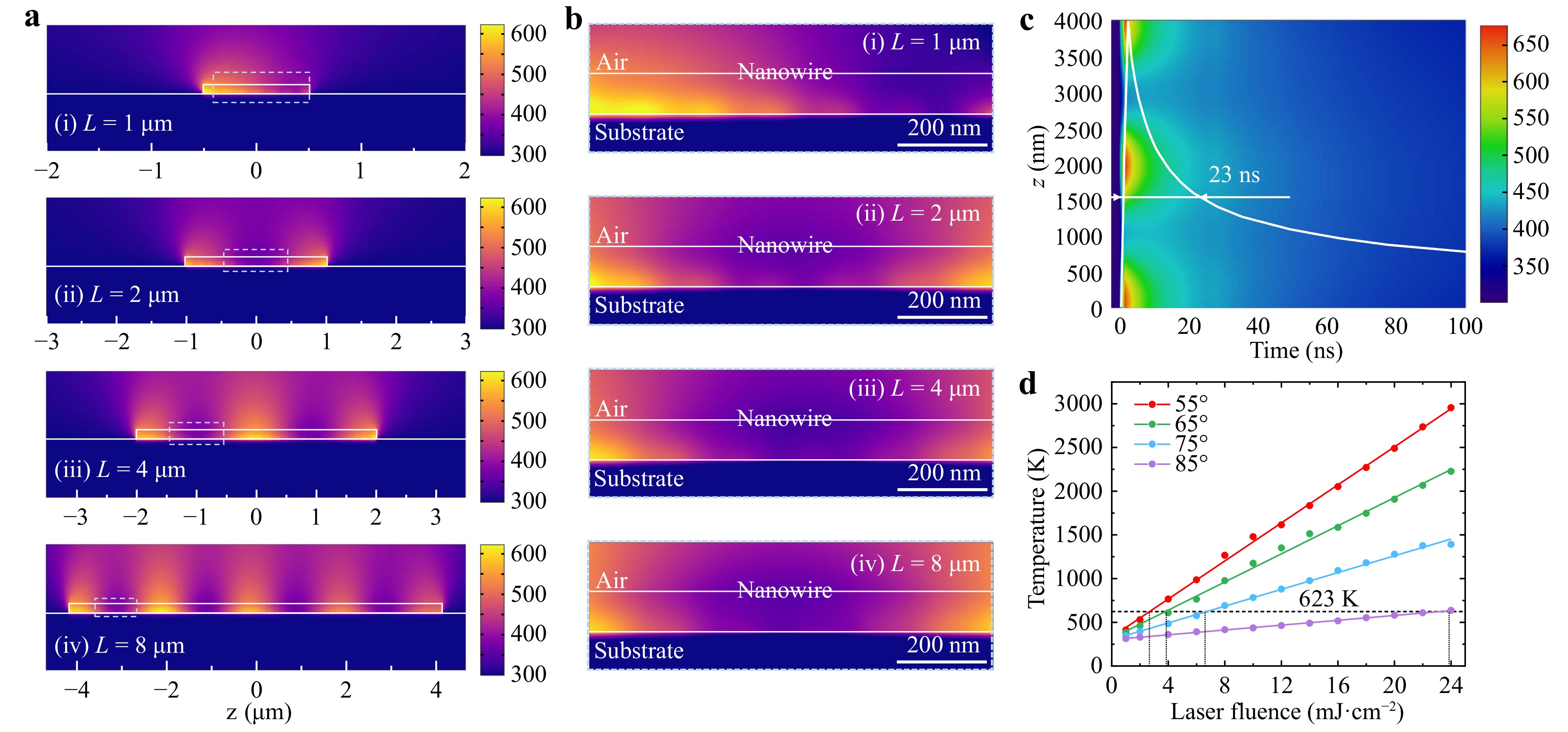
Fig. 3 Self-regulated periodic temperature distribution on a single Ag NW. a simulated temperature distributions for NWs with L = 1 (i), 2 (ii), 4 (iii), and 8 μm (iv) at t = 2 ns under a pulsed laser irradiation (pulse duration ~2 ns) with a laser fluence of 24 mJ cm−2 and θ = 75°, respectively. b close-up views of the areas marked by the light blue rectangles in (a) for better clarification of the sub- and supra- wavelength periods evolution. c transient temperature distribution of a 4-μm-length Ag NW excited by the pulsed light. d maximum achievable temperature (Tm) under a single pulse irradiation versus the laser fluences under different θ.
We also studied the temporal response of an NW system irradiated by a nanosecond pulsed laser. Fig. 3c shows the transient temperature variation of the NW under a single pulse. The temperature reaches a maximum after ~2 ns and then cools down with a thermal relaxation time of 23 ns. To reveal the power threshold for melting NWs, we calculated the dependence of the maximum achievable temperature (Tm) under a single pulse on the laser fluences with different θ (Fig. 3d). Owing to the increasing surface-to-volume ratio, the melting temperature of the NW decreases significantly compared to that of its bulk counterpart53,54. The melting point of the NW used in our model was adopted from experimental results, where Ag NWs with diameters of ~100 nm were split into short fragments at a critical temperature of ~623 K53,54 (black dashed line, Fig. 3d). For a small θ, the slope of the Tm—laser fluence line was steeper than that for a large θ, leading to a decreasing threshold from 23.9 mJ cm−2 to 2.7 mJ cm−2 as θ decreases from 85° to 55°. This can be attributed to the stronger EW excitation at the interface and consequently to the stronger photothermal effects.
-
For the experimental demonstration, we used an oblique-incidence laser irradiation system to generate plasmonic NP arrays and a side-illuminated microscope system to observe the ablation process (Fig. 4a). A commercial supercontinuum white light source (SuperK COMPACT) was used to generate nanosecond laser pulses with a pulse duration of ~2 ns, a repetition rate ranging from 1 Hz to 20 kHz, and an effective wavelength range of 450-500 nm (see Supplementary Information). Using a 50-mm focal distance achromatic lens, the laser pulses were focused into an elliptical spot with a size of ~100 × 40 μm, thereby illuminating the entire NWs under total internal reflection through a silica prism. The laser pulse fluence could be tuned in the range of 0–12.9 mJ cm−2 using a continuously variable neutral density filter. The incident angle of the laser beam could be varied within 50–85° by adjusting the position of the focusing lens to control the final morphology of the periodic nanostructures.
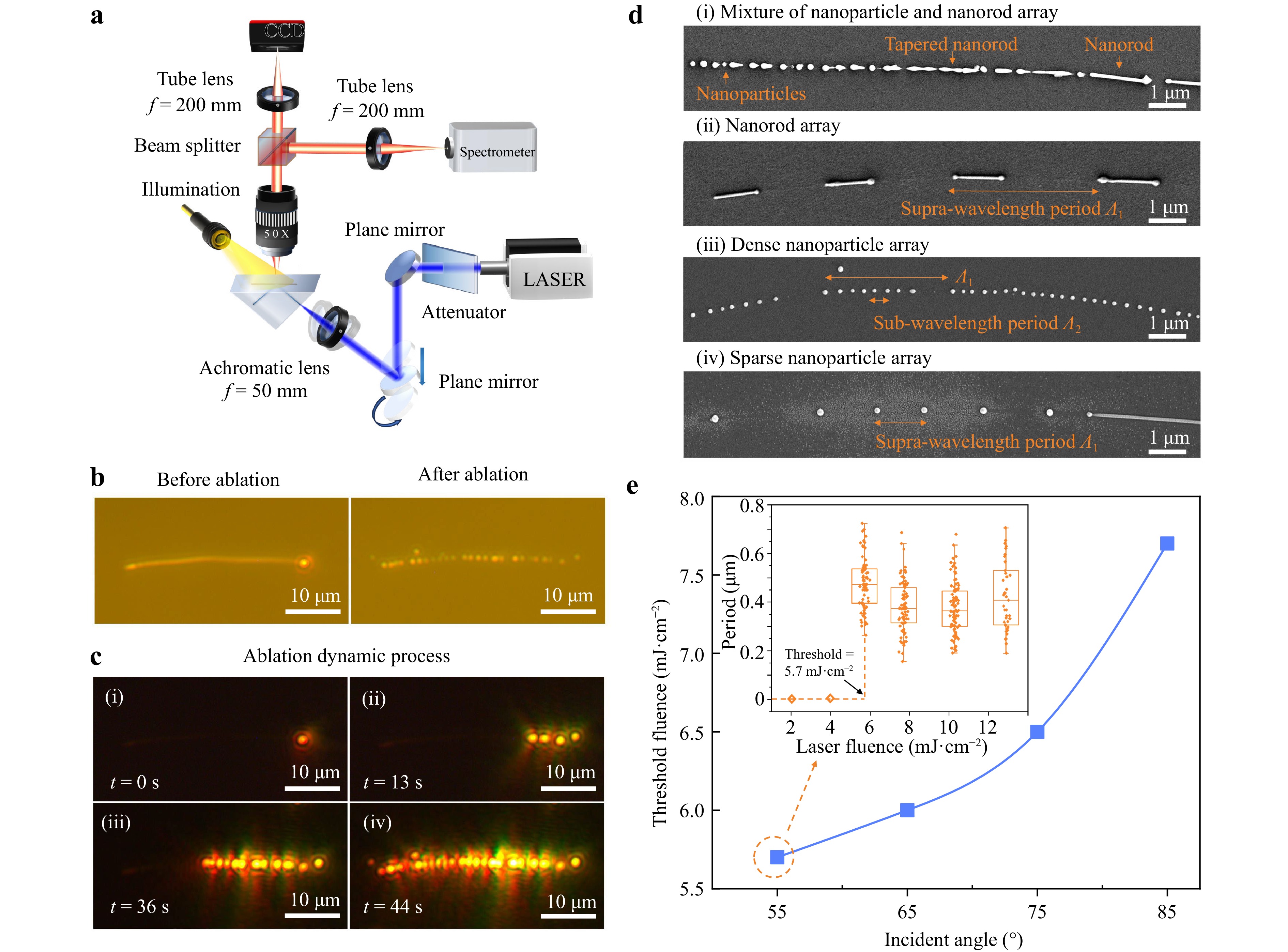
Fig. 4 Experimental demonstration of generating 1D NP arrays from Ag NWs. a Schematic of the oblique-incidence nanosecond pulsed laser irradiation system to fabricate plasmonic arrays and the side-illumination microscope system to observe the ablation process. b Optical microscopy images in bright field of a Ag NW before and after the laser ablation. c Optical microscopy images in dark field of a Ag NW at t = 0 s (i), 13 s (ii), 36 s (iii), and 44 s (iv) after the laser is on, manifesting the ablation dynamics. d SEM images of typical morphologies of the plasmonic arrays, including a mixture of NP and nanorods (i), nanorod (ii), dense NP (iii), and sparse NP arrays (iv). e The dependence of ablation threshold fluence on the incident angle of the laser beam. Inset shows the ablation periods of dense NP arrays versus laser fluence at an incident angle of 55°.
Fig. 4b presents a typical bright-field optical microscopy image of a 90-nm-diameter Ag NW before and after laser irradiation. Fig. 4c further reveals the dynamic ablation process in dark-field views, where bright spots at the ends of the NW can be clearly observed before laser irradiation, thereby indicating that the SPPs are excited and propagated along the NW (Fig. 4c(i)). When laser irradiation starts, the Ag NW gradually breaks into a series of periodically aligned NPs, thereby exhibiting strong scattering (Fig. 4c(ii-iv)).
Depending on the laser exposure time and position of the NW with respect to the laser spot, plasmonic arrays with different morphologies were obtained (Fig. 4d). In Fig. 4d(i), an early stage intermediate state with a mixture of NPs, tapered nanorods, and nanorods (from left to right, Fig. 4d(i)) can be observed. This indicates that the NW first breaks into short NW segments with supra-wavelength periods and then NP chains with subwavelength periods afterwards. When the laser exposure time is sufficiently long (e.g., several tens of seconds at a laser repetition rate of 5 Hz), the NW transforms into a nanorod or NP array (Fig. 4d(ii-iv)). Specifically, if the initial NW is at the periphery of the irradiation spot with a relatively non-uniform laser intensity distribution, the NW tends to shrink into nanorods with supra-wavelength periods (Fig. 4d (ii)) owing to the thermoelastic stresses55. If the initial NW lies at the centre of the irradiation spot with a strong and relatively uniform laser intensity, it decomposes rapidly into an array of NPs with both supra- and sub-wavelength periods (Fig. 4d(iii)). In this case, if the laser irradiation time is longer, photomechanical spallation of some NPs occurs55, leaving behind only supra-wavelength periodically patterned NPs (Fig. 4d(iv)). The required minimum laser fluences (i.e., thresholds) to produce plasmonic arrays increases from 5.5 to 8.0 mJ cm−2 with an increasing θ (Fig. 4e), thereby exhibiting a trend that agrees well with the theoretical calculation in Fig. 3d.
-
Appropriate parameters of the incident laser (e.g., repetition rate = 1 kHz, single-pulse laser fluence = 12.9 mJ cm−2, and illumination of the entire NWs uniformly with the central part of the beam) were chosen. Accordingly, NP arrays with good uniformity in terms of both the NP size and interparticle spacing were obtained. As shown in Fig. 5a(i-iv), a 40-μm-length NW breaks into ~150 NPs with a sub-wavelength period of ~270 nm and an average diameter of ~110 nm, which surpasses the diffraction limit of the light. Most NPs in the arrays exhibit well-defined spherical shapes with smooth surfaces, and are free from observable defects (see the close-up images in Fig. S2)) and notable signs of oxidation (see the EDS spectra in Fig. S4). These merits can effectively reduce the plasmon damping and optical losses. This method is highly suitable for fabricating superlattice nanostructures and provides an interesting platform for manipulating light–matter interaction at the nanoscale22. The dependence of the NP arrays with the sub-wavelength periods on the incident angle of the laser is shown in Fig. 5b. The periods exhibit an overall average value of 270-430 nm with a small fluctuation of ~100 nm, which is almost insensitive to the incident angle, thereby showing good agreement with the simulated trends in Fig 2c. The measured period is approximately two to three times the minimum period (~150 nm) predicted in the simulation results. The deviation may be attributed to the ablation process involving two stages: i) formation of the melt nanospheres in the liquid phase (i.e., pre-structures) with a minimum subwavelength period Λ2 owing to the spatially modulated temperature distribution; ii) regulation of the final geometries by agglomerating the liquated nanospheres under a positive feedback loop provided by the constructive interference between the SPPs and spherical waves excited by the Mie scattering of the pre-structures56–58. In addition, we investigated the dependence of the periods of the sparse NP on the incident angles. As shown in Fig. 5c, the average period increases from ~1000 nm to ~1700 nm as the incident angle increases from 55° to 85°, thereby exhibiting a trend that agrees well with the simulation results in Fig. 2c. Previous studies have demonstrated the decomposition of metal NWs due to Rayleigh instability59,60 when heated at temperatures above the melting point of the NW53,54,61,62. To compare this method with our laser ablation method, heat treatment experiments were performed on the Ag NWs. By pure thermal decomposition, short fragments and nonuniform sized NPs were formed, which exhibited irregular spacings with poor periodicity and large variations in the individual geometries (see Figs. S5-6). Our approach shows good control of the uniformity of the NP sizes and interparticle spacing.
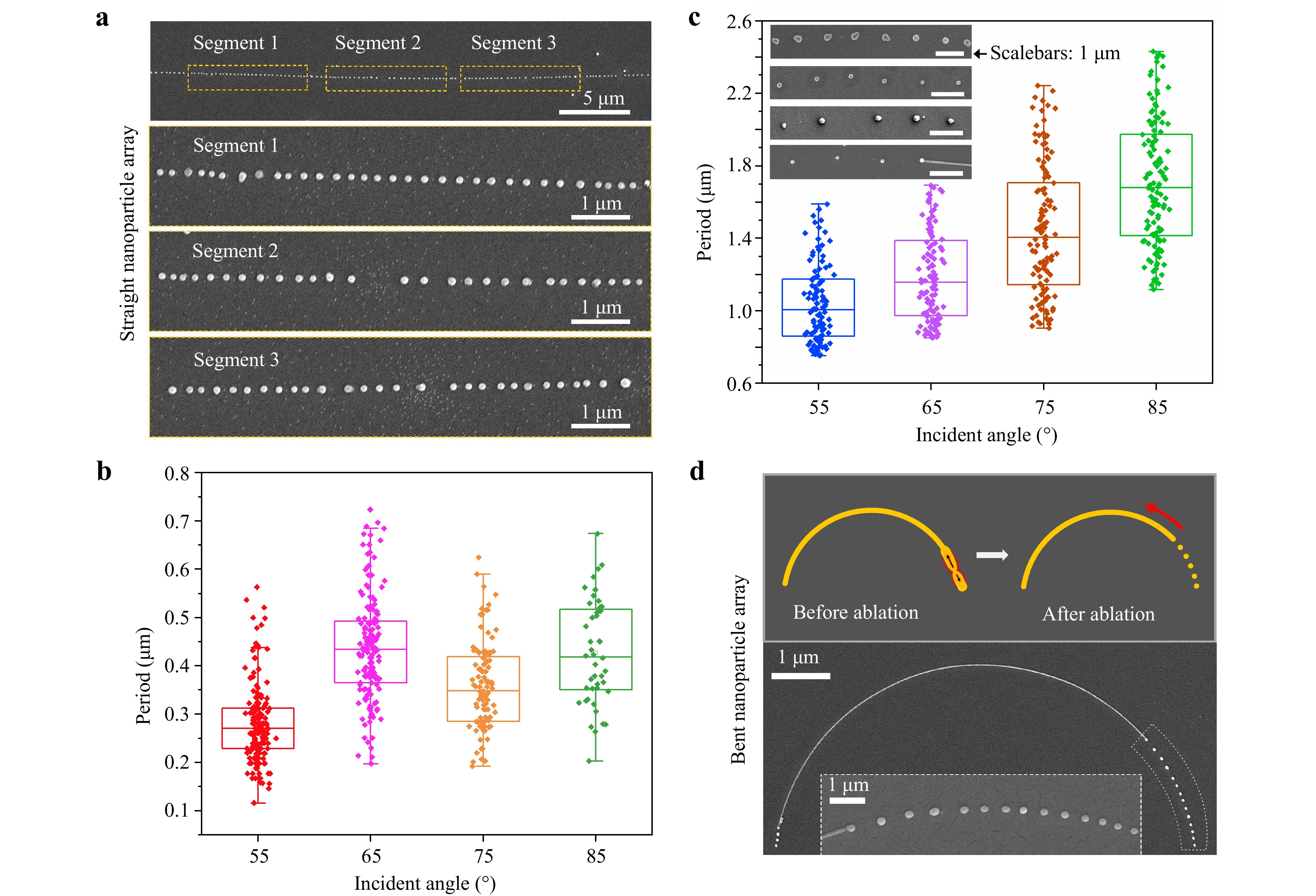
Fig. 5 Generating high-quality plasmonic arrays with tunable parameters. a SEM images of a long-distance dense NP array. Insets (ii-iv) are close-up views of three different segments (marked by orange rectangles) on the NP array in (i). b periods of dense NP arrays versus the incident angle of the laser beam. c periods of sparse NP arrays versus the incident angle of the laser beam. Insets are typical SEM images of the arrays under incident angles of 55°, 65°, 75°, and 85°, from up to bottom, respectively. d schematics (up panel) and SEM images (bottom panel) of curved NP arrays.
In addition to the tunability of periods, the alignment direction of the NP arrays was also modulated. As shown in Fig. 5d, plasmonic arrays can be directly generated on a bent NW, thereby forming NP-based curved arrays that can potentially be used for wearable flexible devices63 and reducing bending losses in highly compact integrated circuits64.
Finally, this method can be extended to generate 1D metal NP arrays directly on curved substrates or microstructures. As a conceptual proof, a single Ag NW was first deposited on an ~1.4-μm-diameter microfibre drawn from a standard optical fibre using the flame-heated taper pulling method65 and then exposed to laser pulses (Fig. 6a). The figure shows that after laser ablation, the Ag NW forms a chain of periodically patterned NPs with a period (~150-240 nm) and an average particle size (approximately 70 nm) beyond the diffraction limit (Fig. 6b), which is highly suitable for high-resolution distributed microfibre optical sensing. Supra-wavelength periods are also obtained. In this case, each NP couples with the whispering gallery mode of the microfibre to form a set of plasmonic-photonic hybrid microcavities with high-quality resonances14 (Fig. 6c-e). The resonance linewidth is compressed to 3.9 nm at a wavelength of ~640 nm (Fig. 6c), corresponding to a Q factor of 164, which is much higher than those of pure microfibres (~10) and a single Ag NP (~10)66. In addition, owing to the variation in the orientations of the NPs on the microfibre surface as well as the slight differences in the individual NP geometries66–68, each NP-microfibre-coupled system exhibits different scattering spectral features and can serve as a unique barcode. As shown in Fig. 6e, approximately six fixed resonance wavelengths exist within the spectral range (indicated by black arrows). Information of the normalized intensity of the resonance peak exceeding 0.5 or not is encoded as “1” or “0”, respectively, thereby indicating the presence (“1”) or absence (“0”) of a certain resonance mode. For example, the barcode of the first NP is read as “011010” (red curve in Fig. 6e). The maximum number of unique barcodes for the coupled system is 26 = 64. Using ten NPs in series, it would be possible to individually tag 26 × 10 ≈ 1018 targets, which can be potentially used in multiplexing applications that require numerous unique barcodes, such as cell tagging, anticounterfeiting, and product labelling69,70.
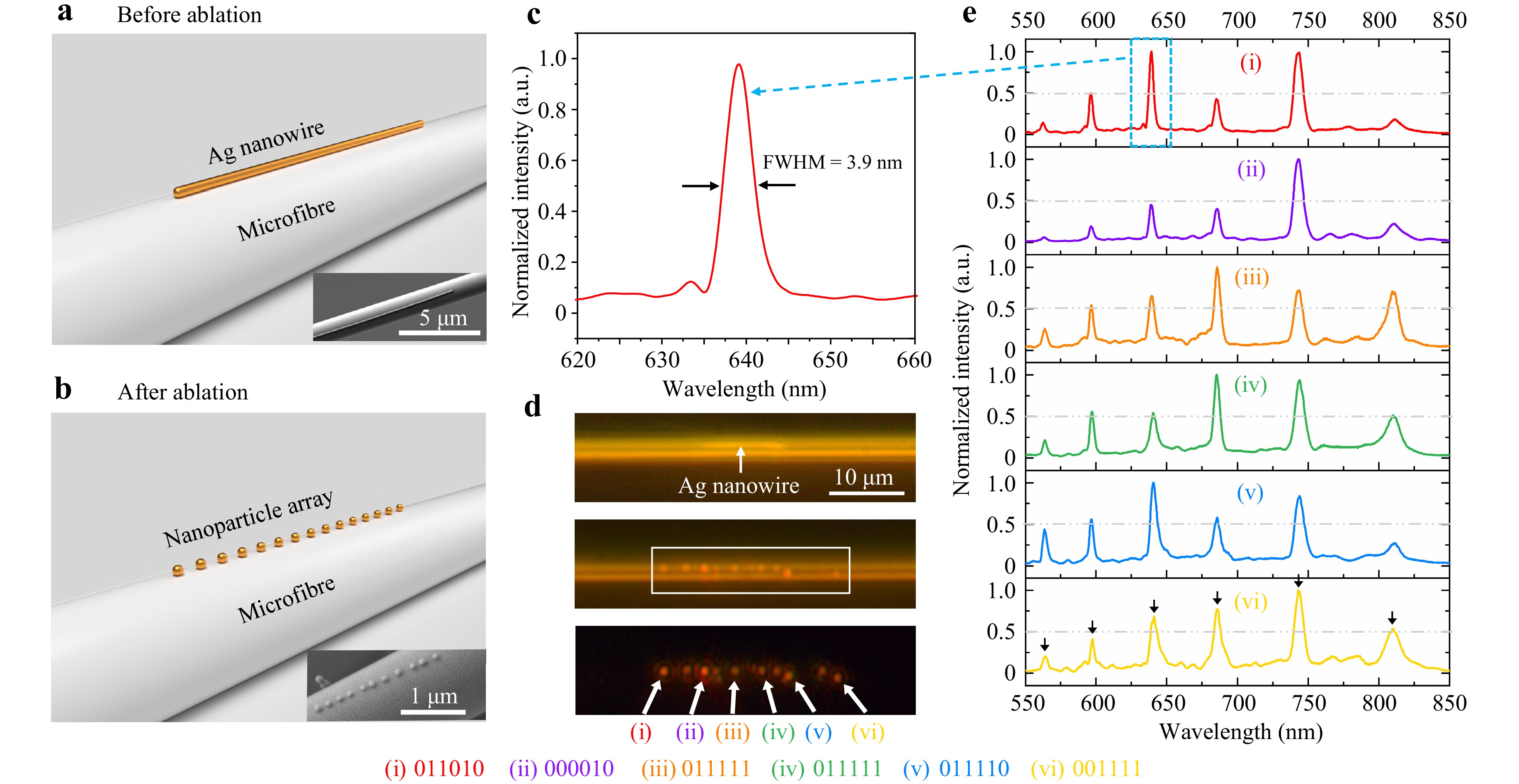
Fig. 6 Generating 1D NP array on microfibres to form a series of microcavities. a schematic of depositing a Ag NW on a microfibre before laser ablation. Inset is a typical SEM image of a Ag-NW-deposited microfibre. b schematic of generating a chain of periodically aligned NPs on a microfibre after laser ablation. Inset is a typical SEM image of an NP-array-deposited microfibre. c close-up view of a resonance peak indicating a narrow resonance linewidth of ~3.9 nm. d optical microscope images of a Ag-NW-deposited microfibre before laser ablation (up). Bright-field (middle) and dark-field (bottom) microscope images of an NP-array-coupled microfibre system, with white arrows indicating the 1st, 3rd, 5th, 7th, 9th, and 11th NP from left to right, marked as (i) to (vi) respectively. e scattering spectra of each NP-microfibre-coupled system in d.
-
In summary, by leveraging tightly confined SPPs on metal NWs and the synergistic effect of standing waves and optical beating, we demonstrated a light-driven approach to fabricate 1D plasmonic arrays with optimized unit structures, tunable interparticle spacing with sub-wavelength or supra-wavelength periods, and flexible alignment directions. This approach leverages tightly confined SPPs and their interference with other waves in a metal NW system, thereby overcoming the limitations of conventional laser direct writing by only a single exposure of a loosely focused nanosecond laser beam to generate self-organized patterns. More importantly, this approach can be extended to fabricate plasmonic arrays directly on curved substrates or microstructures with a spatial resolution beyond the diffraction limit. We demonstrated the fabrication of plasmonic arrays on microfibres, by forming a series of hybrid photon-plasmon microcavities with narrow-band resonance and a barcode system with high multiplexing capacity. We believe that this approach provides a simple, low-cost, and high-efficiency platform for fabricating plasmonic arrays and hybrids that may find applications in plasmonic nanolasing, information encryption, and distributed sensing with high spatial resolution.
-
This work was supported by the Chongqing Natural Science Foundation (Grant Nos. CSTB2024NSCQ-MSX1083 and 1076), Fundamental Research Funds for the Central Universities (No. 2024CDJXY008), National Foreign Experts Program (No. DL2023165003L), and National Natural Science Foundation of China (Nos. 62005032 and 62005031). The authors thank Dr. Yang Zhou for assistance with the SEM imaging and Dr. Weina Han for discussions on the mechanisms of laser nanostructuring.
Generating one-dimensional plasmonic arrays by laser-driven self-organization
- Light: Advanced Manufacturing , Article number: (2025)
- Received: 07 February 2025
- Revised: 03 July 2025
- Accepted: 04 July 2025 Published online: 29 August 2025
doi: https://doi.org/10.37188/lam.2025.057
Abstract: Assembling metal nanoparticles into a well-defined array and constructing strongly coupled hybrid systems enable high-quality resonances with narrow linewidths, which offer new opportunities to circumvent the hurdle of plasmonic losses. Herein, we propose a light-driven approach for generating plasmonic arrays by leveraging the self-organized patterns of tightly confined surface plasmon polaritons in single metal nanowires, which exhibit optimized unit structures, tunable interparticle spacings with supra-wavelength or sub-wavelength periods beyond the diffraction limit, and flexible alignment directions. We theoretically and experimentally show the mechanism of generating field patterns via the interplay of a standing wave and optical beating, followed by the formation of periodic geometries under a spatially modulated temperature distribution. We also fabricate plasmonic arrays on microfibres with diameters down to ~1.4 μm and thereby construct a series of hybrid plasmonic–photonic resonators with narrow-band resonances (~3.9 nm linewidth) as well as a barcode system with high multiplexing capacity. Our results show the potential of simple, low-cost, and high-efficiency fabrication of plasmonic arrays and hybrids that may find applications in plasmonic array lasers, information encryption, and high-resolution distributed sensing.
Research Summary
Laser nano-structuring: Generating plasmonic arrays by light-driven self-organization
Assembling metal nanoparticles into a well-defined array and constructing strongly coupled hybrid systems enable high-quality resonances with narrow linewidths, offering new opportunities to circumvent the hurdle of plasmonic losses. Xiaoqin Wu, Yipei Wang from China’s Chongqing University and colleagues now report a light-driven approach for generating plasmonic arrays by leveraging the self-organized patterns of tightly confined SPPs in single metal nanowires. The arrays exhibit optimized unit structures, tunable interparticle spacings with supra-wavelength or sub-wavelength periods beyond the diffraction limit, and flexible alignment directions. The team also fabricate plasmonic arrays on microfibres and construct a series of hybrid plasmonic–photonic resonators with narrow-band resonances as well as a barcode system with high multiplexing capacity. The results show the potential of simple, low-cost, and high-efficiency fabrication of plasmonic arrays and hybrids especially on non-conducting and curved surfaces.
Rights and permissions
Open Access This article is licensed under a Creative Commons Attribution 4.0 International License, which permits use, sharing, adaptation, distribution and reproduction in any medium or format, as long as you give appropriate credit to the original author(s) and the source, provide a link to the Creative Commons license, and indicate if changes were made. The images or other third party material in this article are included in the article′s Creative Commons license, unless indicated otherwise in a credit line to the material. If material is not included in the article′s Creative Commons license and your intended use is not permitted by statutory regulation or exceeds the permitted use, you will need to obtain permission directly from the copyright holder. To view a copy of this license, visit http://creativecommons.org/licenses/by/4.0/.

 DownLoad: