


-
Perovskite-based devices are a new ”gold rush” for the chemical scientific community. The main research areas are perovskite solar cells with band gaps of 1.5–1.6 eV and current record efficiency higher than 26%1 and light-emitting diode (LED) devices based on CsPbBr3 quantum dots (QDs) with an efficiency higher than 30%2. The rapid progress is attributed to various factors, including the simplicity of device preparation, high charge carrier mobility, defect tolerance, and high light absorption coefficient3–8. In addition, other photovoltaic devices such as photodetectors, light-emitting solar cells, photodiodes, and memristors have been successfully developed due to light-trapping optimisation at the nanoscale9–13. Numerous studies have been performed to improve the efficiency of these devices through various methods, including the design of new device architectures, selection of materials with improved light absorption and charge carrier mobilities, and application of micro- and nanostructures to increase absorption by expanding the effective area14,15. In addition, various nanophotonic approaches can enhance the light absorption. They are usually divided into light management with randomly distributed resonant/non-resonant nanoparticles or regularly orientated array of nanostructures16. In the first scenario, they can be simply used in different positions in perovskite devices17,18. However, such effects as structural colouring, photoluminescence polarisation control, and broadband antireflection can be achieved only with periodic nanostructures19–23.
The fast and precise nanofabrication is a promising approach for the development of micro- and nanoelectronics9. Various anisotropic perovskite layers have been fabricated using a polydimethylsiloxane (PDMS) mould indentation or nanoimprint lithography to improve the light trapping effect in photodetectors24 or solar cells with Moire patterns19. Moreover, nanostructuring of transport layers leads to guided-mode resonances, which has been demonstrated by Feng et al.25. Peng et al.26 have reported a nanostructured TiO2 electron transport layer to increase the fill factor of large-area perovskite solar cells to 84% by creating local regions with a high conductivity. These nanostructuring approaches improve the charge extraction between layers. They have been extensively used for organic, silicon, dye, or tandem devices27 and have become a necessary tool and standard for their synthesis and production. Moreover, periodical nanostructures can introduce structural colour to perovskite devices, which is important for building-integrated photovoltaics28. In the nature, various plants and animals exhibit striking “structural colours”, which are derived from the astoundingly intricate spatial arrangements of inherently colourless biomaterials 29,30.
Periodical nanostructures are also valuable for luminescence and reflection control in perovskite-based devices31. Recently, Wang et al.32 reported that the inherent spin selectivity of excitonic transitions in lead halide perovskites contributes to polarisation effect in their photoluminescence, which can be amplified with functional nanostructuring. The integration of meticulously structured microstructures into perovskite materials has been demonstrated to be a successful method for further improvements in polarisation characteristics of halide perovskite light-emitting devices10. The direct writing with focused ion beam milling on a perovskite surface31 leads to a resonant geometry, with a distinct response in the transverse magnetic (TM) and transverse electric (TE) polarisations21. Recently, Nguyen et al.33 observed Bloch resonances in perovskite QDs placed above a periodical TiO2 grating inducing collective resonances propagating along the grating relief and transforming the unpolarised incoherent emission photoluminescence into a polarised and directed emission signal.
To obtain uniform sub microarrays, photolithography or imprint technologies have been developed over the past decades. However, they suffer from physical limitations in resolution and require multistep micro embossing processing. In addition, some inert oxide-based dense surfaces do not exhibit high plastic deformations or ease of etching to achieve a precise desirable surface relief with lithographic-based fabrication processes. Various ion/electron lithography methods are suitable for the production of precise nanostructures, but are expensive and labour-intensive, as they are multistep manufacturing technologies requiring high vacuums. Although various methods of perovskite nanopatterning have been implemented, there are no reports on application of laser-induced periodic surface structures (LIPSSs) for perovskite nanophotonics and photoluminescence manipulation with light-emitting materials. Invented in 196534 and explained in the 1980s35, the LIPSS formation method has become a powerful and cost-efficient approach for various applications36,37 including surface colouring38,39, antireflection coating40, tribology41, sensing42, diffractive elements43, surface activation44, and surface photo-chemical reactions45. The revolution in powerful ultrafast pulsed lasers makes the surface nanostructuring a low-cost, smooth, with a minimal thermal impact, and time-efficient single-step alternative to lithography. The utilisation of LIPSS for perovskite solar cells or other devices does not largely increase their cost of production compared to the other methods presented above.
In this study, we directly form LIPSS on a TiO2 thin (50 nm) layer to modify optical properties of a halide perovskite layer deposited on top, providing colour-selective reflection and anisotropic photoluminescence. Both wet-chemistry perovskite deposition and LIPSS generation by a cheap nanosecond laser and galvanometer scanner (see Fig. 1) are high-throughput technologies, promising for large-scale fabrication. Moreover, TiO2 is a widely used material as a charge transport layer, and thus the proposed approach is suitable for various perovskite-based optoelectronic devices.
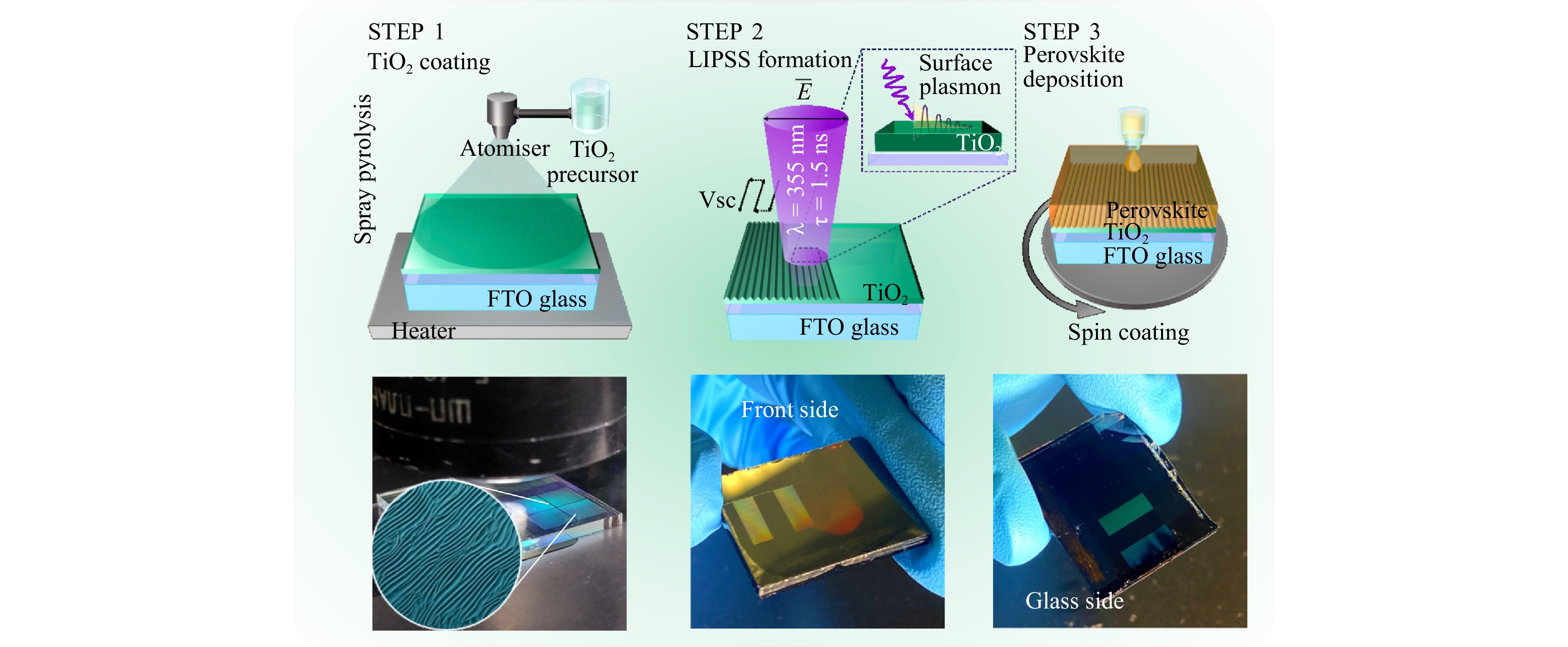
Fig. 1 Schematics of the step-by-step formation of LIPSS-perovskite heterostructures and their photographs before and after perovskite film formation.
-
The LIPSS in the form of a periodic grating was created by the interference of the incident wave with the surface plasmon-polariton excited on the air-TiO2 interface under ultraviolet (UV) laser irradiation46. These structures typically are oriented perpendicularly to the polarisation direction of the laser beam and have a period on the order of the wavelength. Such periodical gratings known as LIPSSs are usually associated with metallic surfaces, but, in some cases, can be formed on dielectric and semiconductor materials47–50. Despite the low optical absorption of transparent oxides in the visible range, LIPSS formation on them has been successfully realised by using pulsed lasers with UV wavelengths, where such materials have higher absorption coefficients, or sacrificial absorbing layers47. When the laser pulse duration exceeds the characteristic electron-phonon relaxation time for the irradiated material, the modulation on the surface recovers the costs in the process of dividing the laser pulse, preserved after its conversion. Thus, to achieve a desirable LIPSS relief on thin films, the surface plasmon wave excitation and interference with the incident beam should be considered to result in a periodic modulation and heat transfer component of the material51. Tsibidis et al.52 included hydrodynamic parameters to consider melting dynamics and resolidification of materials. In our case, the UV laser enabled to very productively fabricate such structures on a TiO2 surface with a mean yield of 2.25 cm2 min−1.
The fabrication of LIPSS was conducted by single-step direct laser processing. 50-nm-thick TiO2 films sprayed on a fluorine-doped tin oxide (FTO)-glass surface were irradiated by the third harmonic of a nanosecond fibre laser in the scanning mode, as shown in Fig. 1. To identify the desired nanostructures, the following irradiation parameters were employed: wavelength λ = 355 nm, pulse width τ = 1.2 ns, repetition rate f = 150, 300 kHz, laser mean power P = 195−381 mW, scan speed VSC = 300−500 mm s−1. To apply different structures, a laser beam focused to a 30 µm spot by an F-theta lens scanned the surface line by line with an overlap between laser tracks over the Y-axis of 83%. With the increase in scan speed or decrease in laser intensity, the period of the gratings decreased slightly from 310 to 290 nm.
For further experiments, three gratings were chosen with periods of 300 ± 13 nm (F = 324 mJ cm−2, VSC = 500 mm s−1), 295 ± 15 nm (F = 360 mJ cm−2, VSC = 500 mm s−1), and 290 ± 10 nm (F = 184 mJ cm−2, VSC = 350 mm s−1), as shown in Fig. 2a-c, respectively. It can be supposed that the LIPSS periods are similar for these three cases. The laser scanning parameters of F = 184 mJ cm−2 and VSC = 350 mm s−1 were marked as optimal due to the absence of melted spaces on the whole surface. According to measured profiles via atomic force microscopy (AFM) shown in Fig. 2d-f, the gratings were rather uniform and covered the whole treated area. Their height varied from 37 ± 3 to 45 ± 4 nm. The grating with a period of approximately 290 nm was most uniform, and thus was chosen for further experiments.
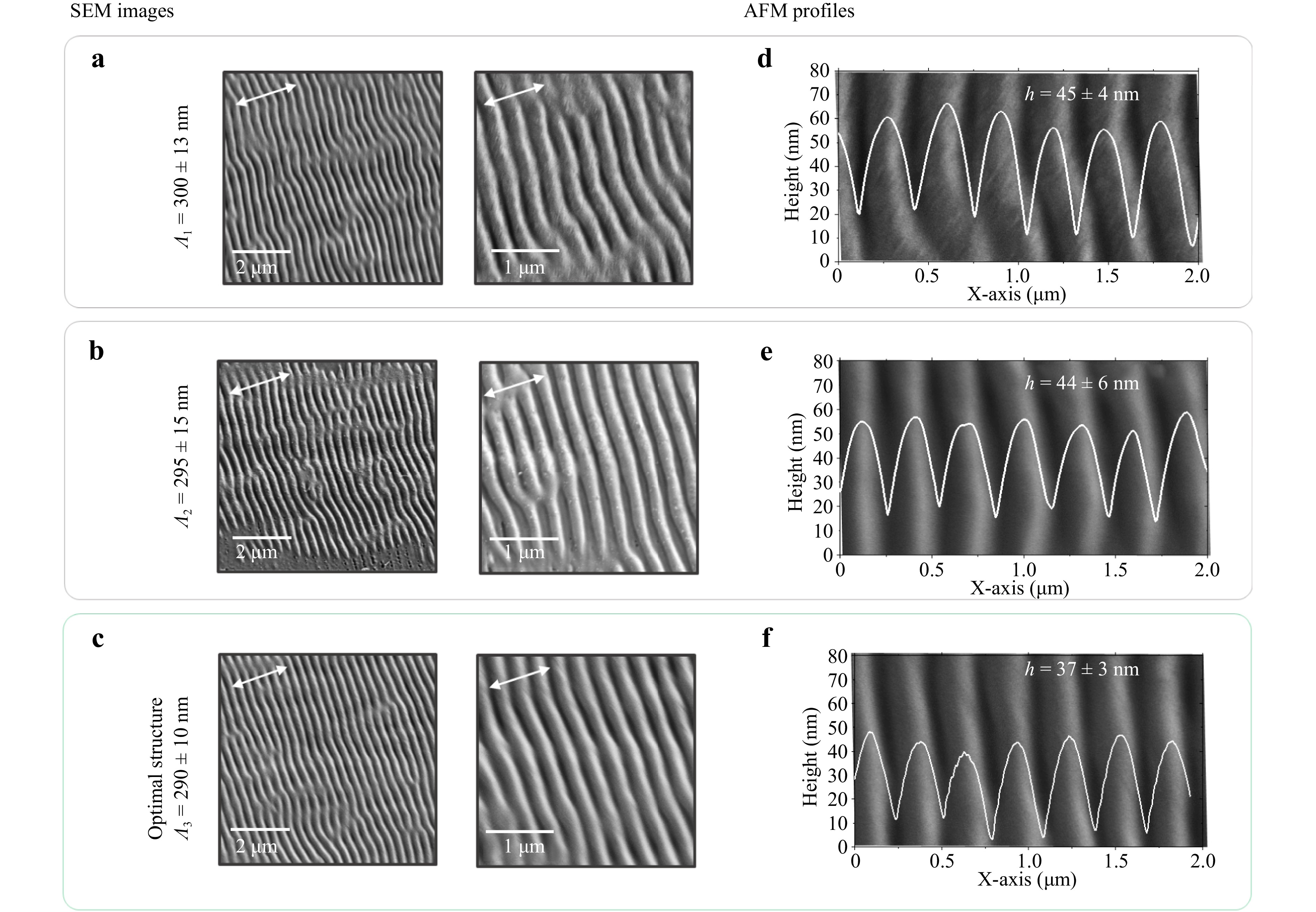
Fig. 2 SEM images a-c and AFM profiles d-f of nanostructured TiO2-covered FTO samples recorded with different periods according to the laser power and scan speed: a 300 ± 13 nm (F = 324 mJ cm−2, VSC = 500 mm s−1), b 295 ± 15 nm (F = 360 mJ cm−2, VSC = 500 mm s−1), and c 290 ± 10 nm (F = 184 mJ cm−2, VSC = 350 mm s−1).
Fig. 3 shows transmittance spectra in the optical near-infrared (IR) region measured for different polarisations of the incident light. To measure the transmittance of the samples and evaluate the intensity changes, a Glan-Taylor prism was introduced in front of the detector. Compared to the plain surface, the structured samples exhibited 10−15% increases in transmittance in the wavelength range of approximately 600−700 nm. The maximum transmittance was detected for the grating with λ3 = 290 ± 10 nm.
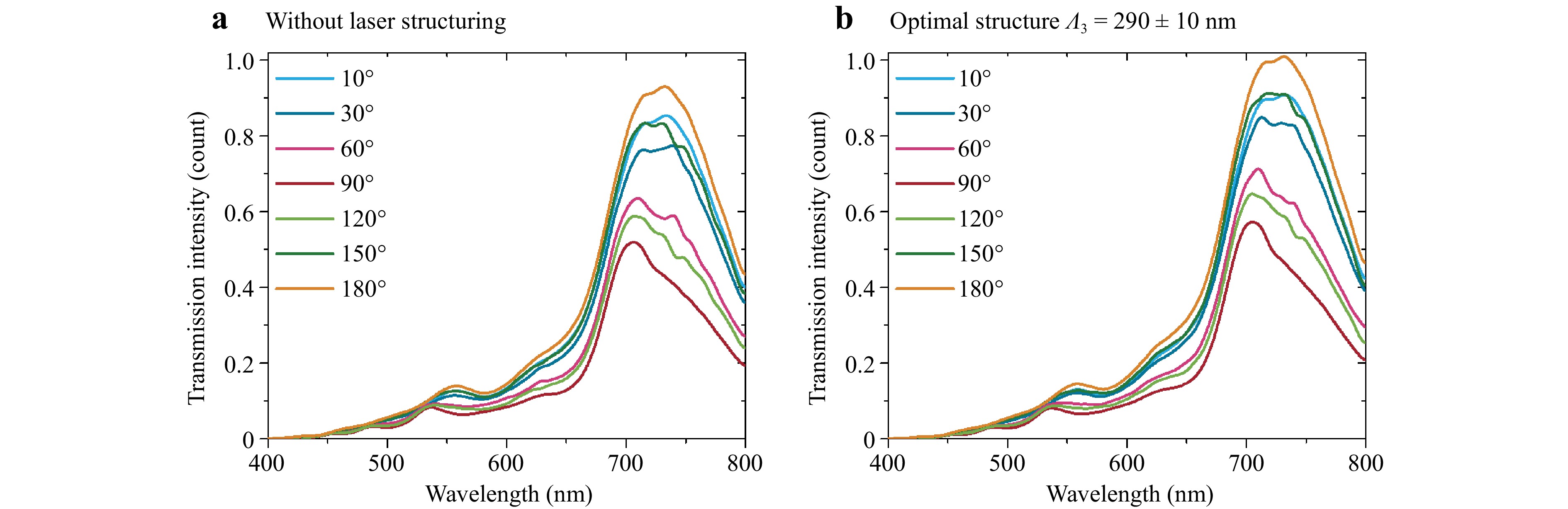
Fig. 3 Optical transmittance of the TiO2-covered FTO glass measured at different polarisation angle rotations (10−180°): a flat TiO2 anatase layer, b nanostructured TiO2 with an optimal structure (290 ± 10 nm; laser processing parameters: F = 184 mJ cm−2, Vsc = 350 mm s−1).
After LIPSS formation, two types of perovskites were chosen as photoluminescence layers. The materials and synthesis steps are described in the Experimental section. According to the scanning electron microscopy (SEM) cross-session profiles in Fig. 4a-d, both CsPbBr3 and Cs0.05MA0.14FA0.81Pb(I0.85Br0.15)3 (or CsFAMAPbIBr3) perovskite layers fully cover the LIPSS TiO2 films without air voids. Thus, to implement these nanostructures for device preparation, additional modification of film devices is not necessary. The thickness of the flat CsPbBr3 film is 150 nm, which changes up to 190 nm in the middle of two bulges. The CsFAMAPbIBr3 film in the untreated TiO2 case has a thickness of 500 nm (approximately 540 nm in the middle of the hills). The nanostructured colouration of the films is visible before and after the perovskite layer deposition from both sides of the substrates (Fig. 1). The structural colour is a result of diffraction, interference, or scattering of light on the periodic or orientated array, which is accompanied by iridescence, an angle- and polarisation-dependent response. The diffracted light wavelength λ can be calculated by the diffraction grating equation: mλ = Λ(cosϕ × sinω + sinβ), where Λ corresponds to the period of the LIPSS, m is the order of diffraction, ϕ is the angle of the light incidence, ω represents the rotation of the LIPSS array within the sample plane, and the angle β corresponds to the deviation of the detector from the LIPSS normal53.
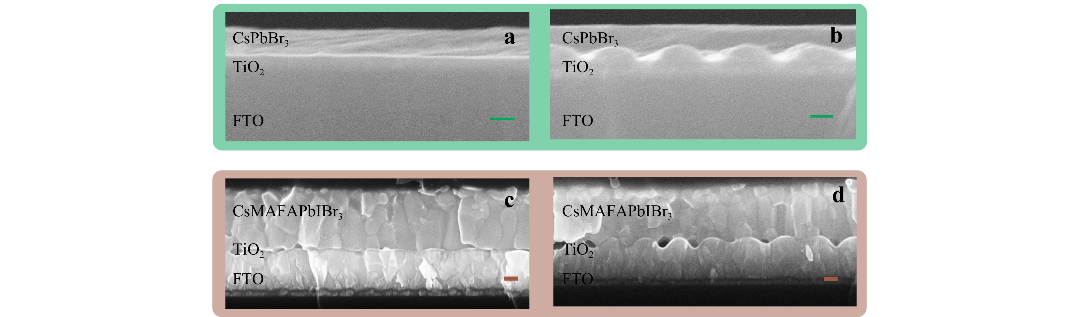
Fig. 4 SEM cross-session of perovskite films deposited on flat and nanostructured TiO2 covered FTO: a flat CsPbBr3 quantum dots, b a CsPbBr3 quantum dot-based film on nanostructured surface, c a CsMAFAPbIBr3 polycrystalline flat film and d a nanostructured CsMAFAPbIBr3 polycrystalline film. Scale bar — 100 nm.
As high-refractive-index materials, lead-based perovskites can possess “structural colours” in the visible range as a result of their nanostructuring and emit photo- or electroluminescence in the IR range (e.g., I-rich perovskites)21, which provides a dual functionality. Fig. S3 illustrates the refraction of incident light by the low-band-gap perovskite CsMAFAPbIBr3 polycrystalline films at a rotation to the light source.
Such LIPSS films can also exhibit an optical polarisation effect including photoluminescence (PL) anisotropy. Fig. 5a-d show changes in PL intensity signal difference according to the angle of the source of light signal collection. The PL signal was collected with a lens with f = 150 mm, filtrated with a pinhole with d = 1 mm, and analysed with a fibre spectrometer (a setup scheme is presented in Fig. S4 together with measurement description). When the light excitation source is polarised and initiates PL of the perovskite layer on the one-direction-oriented LIPSS, collected by a spectrometer, if different PL intensities are obtained depending on the sample orientation, it can be assumed that the samples have PL anisotropy due to the LIPSS. When the LIPSS is oriented parallelly to the PL collecting channel, the PL signal is more efficient and has a uniform intensity in the whole angle range, while it decreases in the perpendicular orientation and has several angle spots (for CsPbBr3 QDs) or areas (for the triple-cation film) of highly emitting states. This is observed for both types of perovskites, but is more emphasised for the CsPbBr3 QDs, which could be explained by their initial high PL quantum yield and optical permittivity and permeability parameters.
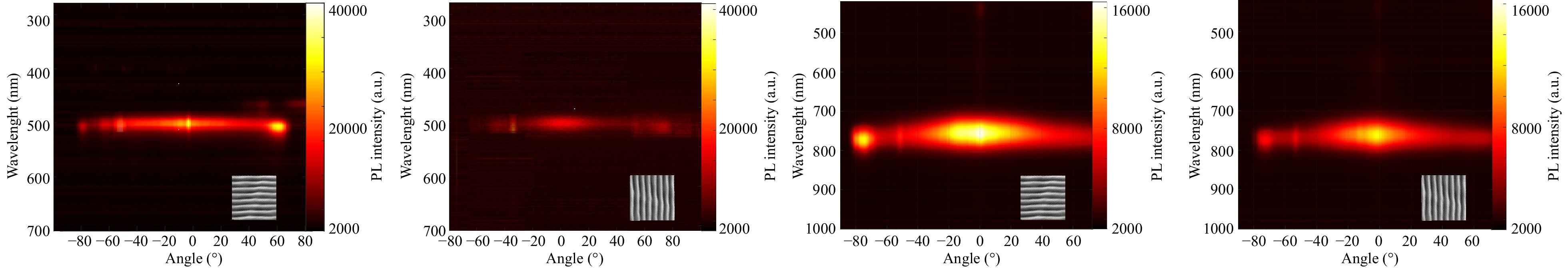
Fig. 5 Photoluminescence intensity dependence on the angle of rotation of the collection channel obtained from perovskite nanostructured films: a, b CsPbBr3 quantum dot films, (c, d) mixed three-cation CsMAFAPbIBr3 polycrystalline film. The nanostructured perovskite films are oriented a, c parallel to the detector rotation and b, d perpendicular to the scanning plane.
The effect of the LIPSS-assisted PL anisotropy was also studied by grating dispersion maps, attributed to the refractive index and material dissipative losses (Fig. 6). The behaviour of the PL output difference for the perovskite films when LIPSS is parallel to the PL input (Fig. 5) can be confirmed by grating dispersions and far-field maps. For CsFAMAPb(IBr)3, the far field and PL dispersion are more uniform. The gap is observed around 45−50° when a dipole is placed in the middle of the perovskite (Fig. 6b, c). This gap becomes lower at a sagittal plane, which is reflected in the experimentally measured PL decrease at 40−60°. However, when a dipole is placed closer to TiO2, the far field (Fig. S5a, b) becomes thinner, and the overall PL signal is more intense at the straight angle. The QDs on LIPSS have numerous “highs and lows” at different angles of PL when the dipoles are placed in the middle of the QD perovskite film.
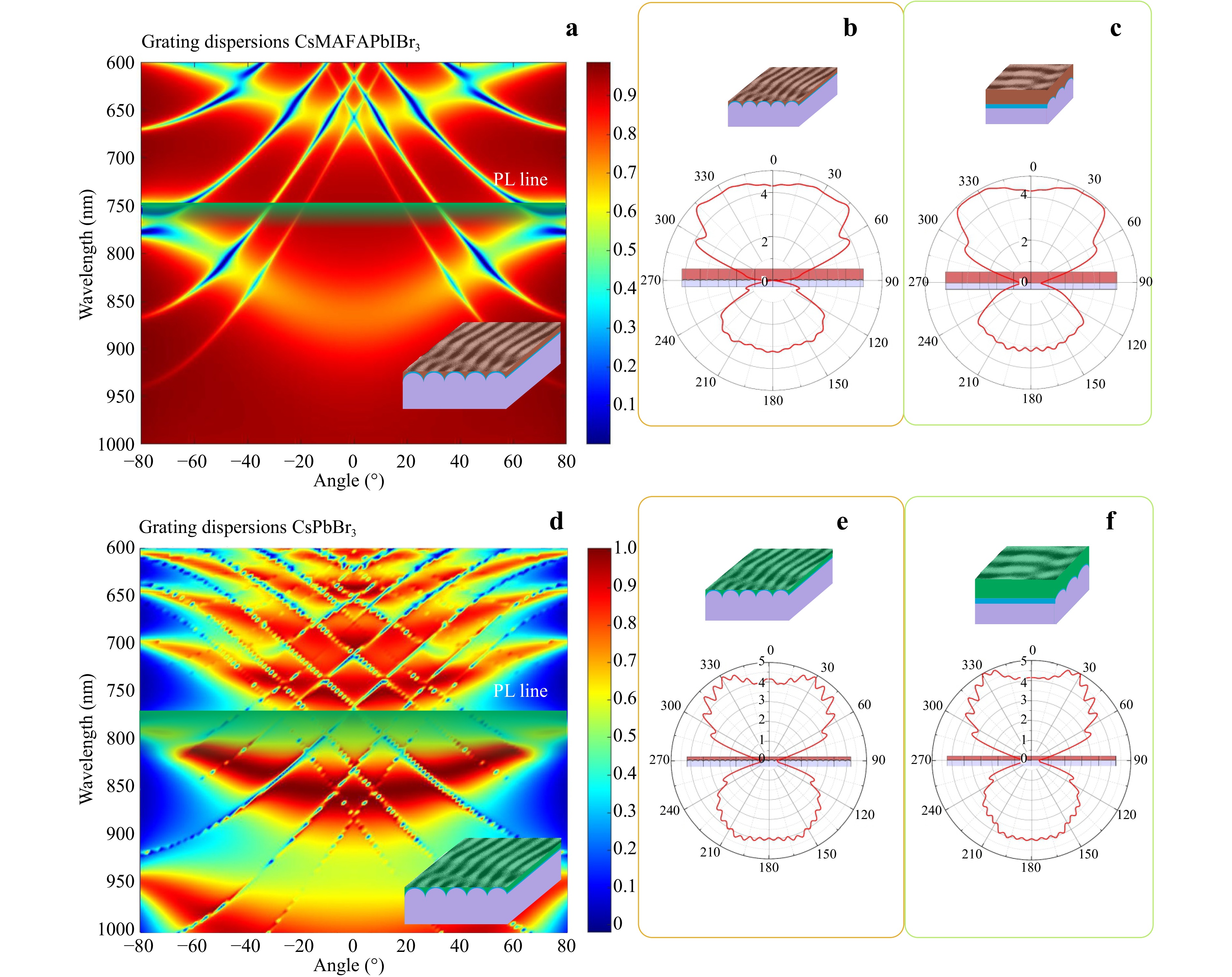
Fig. 6 Calculated angle dispersions of PL intensity for perovskite nanostructured films. a Grating angle dispersion for polycrystalline perovskite CsFAMAPb(IBr)3 film and far field of the dipole at the front b and sagittal c planes of LIPSS when is placed close to TiO2 or in the middle of the perovskite. d Calculated grating angle dispersion for CsPbBr3 quantum dot films placed on the LIPSS layer and far field at the front e and sagittal f planes of LIPSS when is placed close to TiO2 or in the middle of the CsPbBr3 layer.
Moreover, when the dipole is placed close to the TiO2 LIPSS, the number of peaks increases but the back PL signal and wide angle distribution significantly decrease (Fig. S5c, d).
Besides the PL emission behaviour changes, we present PL intensity decay changes. Fig. 7a, b show that the PL decay signal depends on the nanostructured layer. With the presence of any charge extraction layer, the PL time decay decreases for inorganic lead-based perovskites54,55.
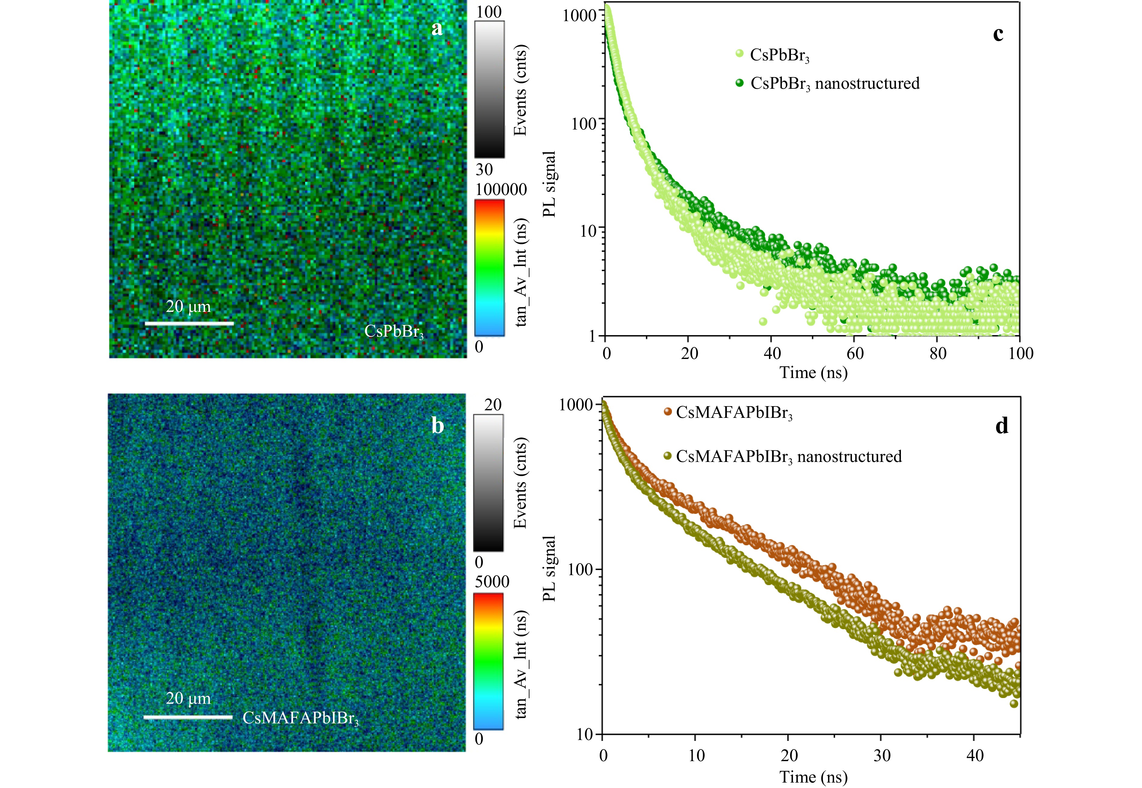
Fig. 7 TRPL of perovskite films. a Two-dimensional (2D) map of the PL intensity decay signal for a nanostructured CsPbBr3 quantum dot film and b CsMAFAPbIBr3 nanostructured polycrystalline film recorded under 405 nm pulsed laser excitation. TRPL decay curves of the nanostructured and flat c CsPbBr3 and d CsMAFAPbIBr3 under a pulsed laser excitation with a wavelength of 405 nm.
The CsMAFAPbIBr3 triple-cation FA-rich perovskite film is generally used for the preparation of perovskite solar cells with high photovoltaic performances26,56,57, where charges are considered in the free state at room temperature58. CsPbBr3 QDs can be utilised to create bright LEDs or optically pumped lasers. For these perovskites, ABC or Shockley-Read-Hall time-resolved photoluminescence (TRPL) decay models can be employed55,59. In this case, the fit by the ABC-model provides information about the relation between recombination rate constants when additional nanostructures or defect states are introduced59,60. The ABC fit formula is
$$ \frac{dn}{dt}=an+bn^2+cn^3 $$ (1) where a, b, and c represent mono-, bi-, and trimolecular charge carrier recombinations, respectively. The fitting enables to analyse first-order process-charge recombination at trap states or charge extraction by the transport layer, reproduced by the parameter a. A second-order charge carrier recombination b is responsible for electron-hole recombination with further photon generation. c reflects the three-body recombination (e.g., Auger recombination) process, whose impact is considerable at a high excitation pump intensity. According to the fitting of the TRPL decay curves, the constant a increases from 2 × 10⁶ s−1 to 9 × 10⁶ s−1 for the nanostructured perovskite film, which is associated with the increase in surface area between TiO2 and perovskite and therefore with charge extraction by the transport layer. The bimolecular recombination constant b is increased for the nanostructured systems from 2.37 × 10⁻¹¹ to 2.23 × 10⁻¹⁰ cm3 s−1. The observed changes in a and b can be explained by the multifunctional role of nanotexturing: increase in light absorption by the perovskite and improved charge extraction.
Recently, Yang et al.61 showed that the charge transport by an electron transport layer changes due to modification of the electrostatic potential and photo-generated electron concentration, which mainly depends on the geometry and height of the array, which can occur in the considered structure. CsPbBr3 QDs were crystallised before film deposition while the triple-cation perovskite was deposited on the substrate and crystallised after spin coating and temperature treatment. Table 1 shows fitting parameters for planar and nanostructured CsPbBr3 films extracted from PL decay curves (Fig. 7c). The slope of the TRPL of CsPbBr3 differs from that of the triple-cation perovskite, which can be associated with the high photoemission gain of the QDs. Thus, we fixed the parameter b for both flat and LIPSS-based films to evaluate if a exhibits any changes. Both a and b significantly differ from those of the CsMAFAPbIBr3 perovskite films due to numerous factors including the presence of free charges and charges at a bound state at room temperature. The crystal size of a single nanoparticle (NP) is 3–4 nm. a for the planar layer of QDs is 1.99 s6, which increases for the LIPSS layer up to 2.5 s6. b is fixed for both, 8.1 × 10⁻¹⁰ cm3 s−1. The increase in a of the TRPL decay can be associated with an increase in surface area between the emitter and charge extractor55. The PL quenching at trapped states and extraction by the transport layer cannot be distinguished solely by TRPL measurements. The X-ray diffraction patterns (Fig. S8) are similar for the perovskite films on flat and LIPSS arrays, and thus the developed LIPSS films do not significantly influence the crystal growth or number of crystal defects. They are not a factor in changing the PL recombination constants. According to the cross-section SEM profile in Fig. 5, the perovskite films on the LIPSS array do not repeat the nanostructuring relief on the external surface, and thus the main changes in PL decay behaviour are related to the perovskite-TiO2 interface. Table 1 shows that the main changes in PL decay are associated with the monomolecular constant a, which is attributed to an increase in charge extraction at the TiO2-perovskite interface. The surface defect passivation method is generally used for the perovskite-top transport layer interface for development of devices such as solar cells62,63. For devices with perovskite QDs, it has been proposed to add various polymers inside the perovskite layer64 that could change the PL decay behaviour and charge extraction on the back transport layer-perovskite.
Film type a, s−1 b, cm3 s−1 CsMAFAPbIBr3 planar 2.00 × 10⁶ 2.37 × 10⁻¹¹ CsMAFAPbIBr3 nanostructured 9.00 × 10⁶ 2.23 × 10⁻¹⁰ CsPbBr3 QDs planar 1.99 × 10⁶ 8.1 × 10⁻¹⁰ (fixed) CsPbBr3 QDs nanostructured 2.50 × 10⁶ 8.1 × 10⁻¹⁰ (fixed) Table 1. TRPL recombination constants of CsMAFAPbIBr3 and CsPbBr3 QDs films deposited on planar or nanostructured substrates, obtained with the ABC model fit
-
We propose a novel approach for modification of halide perovskite optical properties (reflection and photoluminescence) by means of LIPSS with a subwavelength period on a TiO2 film substrate, which is generally used as a charge transport layer for perovskite optoelectronic devices. The proposed LIPSS-based method has a high productivity (2.25 cm2 of treated area per minute), is reproducible, and prevents perovskite film deformation, damage, or spoiling. We tested nanostructures for two types of perovskites, which have modified directivity patterns of photoluminescence depending on the LIPSS orientation and are supposed to improve photon recycling together with charge extraction, confirmed by TRPL constant measurements. Our novel approach provides new degrees of freedom in the manufacturing of advanced perovskite optoelectronic devices. We envision further development of this field by direct LIPSS formation on functional perovskite layers, which is still very challenging to achieve by modern laser technologies65.
-
CsMAFAPb(IBr)3: Chlorobenzene (CB, anhydrous, LenReaktiv), N,N-dimethylformamide (DMF, anhydrous, 99.8%, Sigma Aldrich), dimethyl sulfoxide (DMSO, anhydrous, ≥ 99.9%, Sigma Aldrich), lead bromide (PbBr2, 99.999%, LenReaktiv), lead(II) iodide (PbI2, 99.999%, LenReaktiv), formamidinium iodide (FAI, 99.99%, trace metal basis, GreatCell Solar), methylammonium bromide (MABr, 99.99%, trace metal basis, GreatCell Solar), and caesium iodide (CsI, 99.999%, trace metal basis, Sigma Aldrich) were employed.
CsPbBr3: Caesium carbonate (Cs2CO3, 99.9%, Sigma Aldrich), oleic acid (OA, 90%, Sigma Aldrich), trioctylphosphine (TOP, 90%, Sigma Aldrich), oleylamine (OLA, technical grade, 70%, Sigma Aldrich), lead(II) acetate trihydrate (99.99%, ChemCraft), lead(II) bromide (PbBr2, 99.999%, ChemCraft), tetramethylammonium bromide (Me4NBr, 98%, ChemCraft), lecithin (90%, Thermo Scientific Chemicals), cetane (98%, Ekos-1), toluene (99.5%, Ekos-1), and bromine (99.3%, LenReactiv) were employed.
TiO2: Ethanol (99.5%, LenReaktiv), titanium diisopropoxide bis(acetylacetonate) (75 wt.% in isopropanol, Sigma Aldrich), and acetyl acetone (99%, Sigma Aldrich) were used.
-
The FTO substrates have been cleaned from pollution by a soap, deionised (DI) water, and isopropanol for 10 min three times in an ultrasonication bath. For TiO2 spray deposition, FTO substrates were heated from room temperature to 460°C. A layer of TiO2 was deposited 20 times with an interval of 10 s between depositions on the heated FTO substrates to 460°C using an airbrush. The spray solution was composed of ethanol, acetyl acetone, and titanium diisopropoxide in a volume ratio of 90 : 4 : 6. The atmosphere gas in the airbrush was at a pressure of 1.5 bar. Afterward, the sprayed glass samples were slowly cooled to room temperature. Before perovskite deposition, the FTO-TiO2 films were treated under UV light for 20 min.
CsMAFAPb(IBr)3: CsI, MABr, FAI, PbBr2, and PbI2 were dissolved in a DMF:DMSO solution (9 : 1) to obtain 1.38 mmol perovskite with a chemical formula of Cs0.05MA0.14FA0.81Pb(I0.85Br0.15)3. 70 µL of the perovskite precursor was dispensed on the FTO-TiO2 film, just after the UV exposure, transferred to a glovebox, and immediately spun at 4000 rpm for 35 s. At 15 s to the end, 185 µL of CB was carefully dispensed on the perovskite film, and then the substrate was dried at 100°C for 10 min.
CsPbBr3 QDs: Caesium carbonate (1.628 g, 5 mmol), OA (5 mL, 16 mmol), and cetane (20 mL) were mixed in a 50 mL flask connected to a Schlenk line. The mixture was then placed in an oil bath preheated to 80°C (in this case, the mixture foamed less and did not spill into the line). Afterward, as the reaction mixture heated, the vacuum valve was carefully opened to prevent excessive boiling of the reaction mixture. The mixture was kept at 120°C and under vacuum (0.1–0.5 mbar) until the salts were completely dissolved and the water release ceased. Lead(II) acetate trihydrate (4.607 g, 12 mmol), OA (7.6 mL, 24 mmol), and cetane (16.4 mL) were mixed in a three-neck flask, gradually heated to 120°C, and evacuated (0.1 mbar) until complete evaporation of acetic acid and water. TOP (6 mL, 13 mmol) and bromine (0.6 mL, 11.5 mmol) were carefully mixed in an inert atmosphere. The resulting TOP-Br2 was dissolved in toluene (18.7 mL) after the reaction was completed and cooled to room temperature. To prepare a passivating mixture (PM), 10 mL of 1-Octadecene (ODE), 0.5 mL of OA, 0.5 mL of OLA, PbBr2 (100 mg, 0.27 mmol), and Me4NBr (126.0 mg, 0.81 mmol) were added to a round-bottom flask, and the mixture was heated to 120°C overnight. Cs-oleate (4 mL, 1.6 mmol), Pb-oleate (5 mL, 2.5 mmol), and lecithin (0.324 g, 0.45 mmol) were then dissolved in the mixture of cetane (10 mL), OA (1 mL), and OLA (1 mL) and heated under vacuum to 100°C for 0.5 h. The atmosphere was changed to nitrogen, the mixture was heated to 120°C, and, after 3 min, two solutions of TOP-Br2 in toluene (5 mL, 5 mmol of Br) and PM (2 mL) were injected. After 3 s from the injection, the reaction mixture was placed in an ice bath with a constant stirring using a magnetic stirrer. The crude solution was precipitated by the addition of two volumetric equivalents of methyl acetate, followed by centrifugation at 29,500 g for 10 min. The precipitated fraction was dispersed in 15 mL of toluene, 1 mL of PM was added, and the resulting mixture was stirred for 5 min. Afterward, 30 mL of methyl acetate was added, and the mixture was centrifuged. The dissolution and precipitation procedure was repeated using half-volumes of the solvents and PM. After the last precipitation, QDs were dispersed in 2 mL of toluene and centrifuged at 29,500 g again for 1 min to remove any nondispersed residue. The QD mixture was deposited on FTO TiO2 substrates, spun at 1000 rpm for 60 s, and then dried at 50°C to evaporate liquids for 15 min.
-
For grating fabrication, a commercially available laser system (Minimarker 2-UV, Laser Centre LLC, Russia) was used. The system is based on a nanosecond pulsed ytterbium fibre laser operating at the third harmonic (λ = 355 nm). The laser generates 1.2 ns pulses with a pulse energy up to 9.3 mJ with a repetition rate of 10−300 kHz. The system was equipped with a two-axis galvanometer scanner allowing precise movements of the laser beam over the sample and F-theta lens focusing the beam to a 30 µm spot within a field of 110 × 110 mm2.
-
For the simulations of angle-resolved reflection spectra, a custom-written code utilising the Fourier modal method was employed. This method entails expansions of the electromagnetic field and permittivity function into Fourier series. The reflectance is computed by solving the wave equation within the discretised Fourier space while adhering to the appropriate boundary conditions. The efficiency of this approach was augmented through utilisation of adaptive coordinates, enabling to attain a relative error of 10−4 by considering eight Fourier harmonics in the expansion. The far-field directivity patterns from perovskite nanostructured films were obtained in the license program package for full-wave numerical simulations CST Microwave Studio (Time-Domain Solver). The calculated structure has a square geometry with 10 unit cells per length. The period is equal to 120 nm. The calculations were performed for two types of perovskite materials: CsFAMAPb(IBr)3 and CsPbBr3. The excitation source was inserted into the centre of the lattice within the layer of perovskite material. The open (with space) boundary conditions were set in the x-, y-, and z-directions to circumvent potential minor reflections. To calculate the far-field directivity of the structure with the polycrystalline perovskite CsFAMAPb(IBr)3 film, a 750 nm far-field monitor was added. The far-field directivity of the structure with CsPbBr3 QD films was calculated under a 500 nm far-field monitor.
-
The cutting planes of the perovskite hybrid films were studied using SEM (Zeiss Supra 25, Carl Zeiss, Oberkochen, Germany) at an accelerating voltage of 20 kV at 300 pA. The transmittance dependence on the angle polarisation of the substrates was evaluated with a setup with a collimated white light (halogen lamp) transmitted through the sample and collected by a light detector placed above a polariser filter with a 150 l/mm grating, which was rotated according to the LIPSS.
PL intensity-scanning angle maps of perovskite films were acquired with the original setup. A continuous-wave (CW) laser diode with a wavelength of 405 nm was used as a radiation source to excite PL from both types of perovskite films. The radiation power was then controlled using a variable neutral-density filter (at 5 mW). The radiation was downsized with a telescope and focused on the sample using a lens with f = 150 mm. The sample was mounted on a three-coordinate translator with a possibility of additional rotation in the plane perpendicular to the excitation optical axis. The luminescent signal was collected with a lens with f = 150 mm, filtrated with a pinhole with d = 1 mm, and analysed with a fibre spectrometer (AvaSpec-2048 Avantes). The collection channel was rotated around the sample. The sample was oriented in two positions at which the grating was oriented perpendicularly and parallelly to the scanning plane. A scheme of the setup is presented in Supplementary Information. TRPL maps were obtained at room temperature by a laser scanning confocal microscope MicroTime 100 (PicoQuant) equipped with Plan N 100× (numerical aperture (NA) = 0.90) (Olympus) objectives and picosecond pulsed diode laser head (λ = 405 nm) with a pulse repetition rate of 1 MHz. The average laser power of the picosecond pulsed diode laser was 14.4 nW for the CsMAFAPb(IBr)3 films (control and with LIPSS-TiO2), controlled by a power meter, while that for the CsPbBr3 QDs-based films (control and with LIPSS-TiO2) was 1.5 nW.
-
The investigation of the gratings via SEM (Fig. 2) was carried out at the Interdisciplinary Resource Center for Nanotechnology of Saint Petersburg State University within the framework of project no. AAAA-A19-119091190094. This study was supported by the Russian Science Foundation (project no. 24-62-00022) and Priority 2030 Federal Academic Leadership Program.
Structural colouring and luminescence anisotropy of perovskite thin films via laser-induced periodic surface structure formation
- Light: Advanced Manufacturing , Article number: (2025)
- Received: 23 December 2024
- Revised: 04 August 2025
- Accepted: 04 August 2025 Published online: 22 September 2025
doi: https://doi.org/10.37188/lam.2025.062
Abstract: Perovskite nanostructured films are essential to create advanced optoelectronic and photovoltaic devices because of the additional degrees of freedom of manipulation by light reflection and structural colouration, as well as by light trapping and localisation, resulting in control of intensity or polarisation of luminescence. In this paper, we report structural colouration and photoluminescence anisotropy in perovskite films deposited on a substrate with laser-induced periodic surface structures (LIPSSs) on a thin TiO2 layer. The LIPSS TiO2 layer improves charge extraction from the perovskite films, confirmed by a time-resolved photoluminescence analysis. The developed method of substrate nanostructuring does not damage the perovskite films, in contrast to direct laser ablation, imprinting by a mould, mechanical scratching with a cantilever, or plasma-chemical etching. Moreover, the LIPSS formation is appropriate for upscaling owing to the high speed of LIPSS writing (2.25 cm2min-1) and uniform surface nanostructuring.
Research Summary
Luminescence anisotropy of perovskite films deposited on laser-induced periodic surface structures
Perovskite nanostructured films play a crucial role in the development of advanced optoelectronic and photovoltaic devices due to their additional degrees of freedom in terms of light manipulation, including reflection, structural coloration, trapping, and localization. Aleksandra Furasova from ITMO University and colleagues report on the structural coloration and photoluminescence anisotropy of perovskite films deposited on substrates with laser-induced periodic surface structures (LIPSS) on a thin titanium dioxide (TiO2) layer. The LIPSS TiO2 layer enhances charge extraction from the perovskite film, as confirmed by time-resolved photoluminescence analysis. The method of perovskite nanostructuring does not damage the perovskite films, unlike other methods such as direct laser ablation, mold imprinting, mechanical scratching and plasma-chemical etching. Furthermore, the LIPSS process is suitable for upscaling due to the high rate (2.25 nm2/min) and uniform of LIPSS formation.
Rights and permissions
Open Access This article is licensed under a Creative Commons Attribution 4.0 International License, which permits use, sharing, adaptation, distribution and reproduction in any medium or format, as long as you give appropriate credit to the original author(s) and the source, provide a link to the Creative Commons license, and indicate if changes were made. The images or other third party material in this article are included in the article′s Creative Commons license, unless indicated otherwise in a credit line to the material. If material is not included in the article′s Creative Commons license and your intended use is not permitted by statutory regulation or exceeds the permitted use, you will need to obtain permission directly from the copyright holder. To view a copy of this license, visit http://creativecommons.org/licenses/by/4.0/.

 DownLoad: