


-
The growing demand for high-performance, energy-efficient systems in advanced industries such as artificial intelligence has driven the development of advanced semiconductor devices1. Fabricated using highly integrated and state-of-the-art processes2,3, these devices require precise inspection at every manufacturing stage to ensure quality and reliability. Electron beam-based methods like scanning electron microscopy (SEM)4 and transmission electron microscopy (TEM)5 achieve sub-nanometer spatial resolution but are limited by their destructive nature and slow operation, making them less ideal for high-throughput environments6. Consequently, there is growing interest in non-destructive optical inspection technologies, including confocal microscopy7−9, interferometry10−13, and other advanced techniques14−16. However, accurately measuring the surfaces and internal structures of micro-patterned three-dimensional stacked integrated circuit (3D-IC) devices with high aspect ratio (HAR) structures presents significant challenges due to severe scattering effects17,18 and low signal-to-noise ratio (SNR)19−22. This is particularly critical for structures like Cu-filled through silicon vias (TSVs), which serve as electrodes in high-bandwidth memory (HBM) and other advanced applications23. Incorrect TSV depths can lead to open circuits or substrate damage problems. Recent techniques24 using spectral interferometry, with absolute phase information of polarized broadband light, enable the measurement of TSV depth and asymmetry even in the presence of multilayers or surrounding patterns. However, the low penetration depth of light in metals makes inspecting the structures and dimensions of Cu-filled TSVs difficult, underscoring the importance of developing reliable techniques for precise measurements.
The complex micro-patterns on the front side and the presence of Cu-filled TSVs in manufactured 3D-ICs make it challenging to measure and inspect their internal structures using the conventional front-side illumination approach. To overcome these difficulties, an alternative method involves illuminating the backside of the sample with infrared (IR) wavelengths, which can penetrate the silicon wafer (Fig. 1). Previously, IR spectral interferometry with an objective lens was used to measure TSV structures from the backside of a silicon wafer with high spatial resolution25−27. In this backside measurement approach, the measured depth is determined by the optical thickness, which necessitates accurate determination of the silicon wafer’s refractive index for reliable results28. Because current IR spectral interferometry techniques only measure optical thickness, an additional procedure for refractive index measurement and a calibration process are required to accurately characterize TSV depth. Moreover, the refractive index of silicon is not constant, but varies depending on factors such as crystal structure29, doping30,31, temperature32, and spatial non-uniformity33, typically in the range of 10−3 to 10−2. Several interferometric approaches have been proposed for the simultaneous measurement of thickness and refractive index; however, existing methods either require mechanical z-axis scanning, which limits throughput34 or rely on collimated beams with millimeter-scale spot sizes, which lack the lateral resolution necessary for inspecting fine TSV structures28. Recently, a chromatic confocal spectral interferometry method was introduced to measure both thickness and refractive index in glass35. However, its accuracy is limited by uncertainty in the effective NA (arising from nonlinear elements in the sensor) and by dispersion in the reference arm. Moreover, the method is not suitable for silicon samples, as the 810–860 nm wavelength range provides insufficient penetration for backside inspection. These constraints underscore the need for a new measurement system capable of accurately and reliably inspecting silicon devices from the backside.
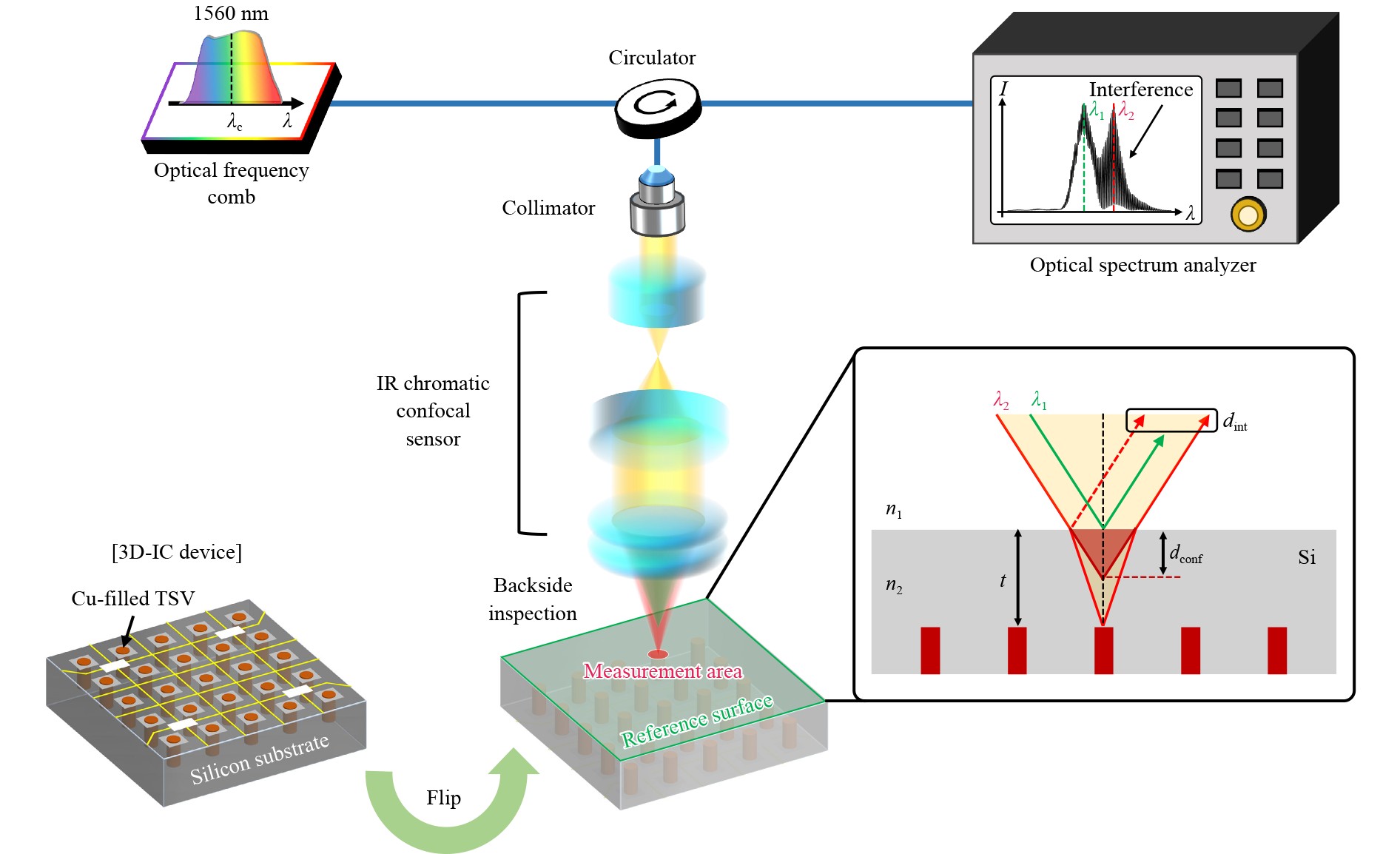
Fig. 1 Principles of the backside silicon inspection systems. Operation principle of backside inspection on a silicon substrate containing Cu-filled TSVs and experimental setup of the IR chromatic confocal spectral interferometry. A 1560 nm optical frequency comb is used as a light source to penetrate silicon. An IR chromatic confocal sensor is employed to identify the centre wavelengths of the signals reflected from the top and bottom surfaces ($ {\lambda }_{1},{\lambda }_{2}) $, as well as their interference signals.
Here, we present an IR chromatic confocal spectral interferometry technique that simultaneously measures both the thickness and refractive index of silicon samples, achieving a consistently high spatial resolution (~14 μm beam size) across all Z-axis positions without the need for vertical scanning, and simultaneously overcoming the limited penetration depth in silicon, NA-related and dispersion-related accuracy issues inherent in previous implementations. By employing an optical frequency comb centred at 1560 nm with a 70 nm optical bandwidth as a light source, we have developed, for the first time in the IR wavelength range, a chromatic confocal sensor optimized for limited optical bandwidth conditions through optical simulation. A silicon wafer with a thickness of 534.2 μm was measured with a repeatability of 72.3 nm and an uncertainty of 560.7 nm (k = 1). The hole depth profile of a silicon sample fabricated using the Deep Reactive Ion Etching (DRIE) process was also measured from the backside. Furthermore, we achieved the first successful measurement of Cu-filled TSV depths in commercial memory products using IR spectral interferometry with a high-NA lens, enabling high-precision depth measurements for both individual Cu-filled TSVs and TSV arrays under different NA conditions.
-
The operation principle of the proposed backside silicon inspection system is illustrated in Fig. 1. This system enables the simultaneous measurement of silicon’s refractive index and thickness with high spatial resolution. Wavelength-to-height encoding is achieved using an IR chromatic confocal sensor with a broad-spectrum Er-fibre optical frequency comb centred at 1560 nm. Spectral signals from both the top and bottom surfaces of the silicon wafer are detected by an optical spectrum analyser (OSA). A low-pass filter is then applied to the acquired optical spectrum to extract the centre wavelengths of the reflection signals. By referring to a pre-established wavelength-to-height lookup table (LUT), the chromatic confocal distance ($ {d}_{conf} $), defined as the distance between reflections from the top and bottom surfaces, is determined. Additionally, by using the pattern-free top surface as a reference plane, the interference signal from the bottom surface can be measured, yielding $ {d}_{int} $, which corresponds to the optical thickness of the wafer thickness. From the measured $ {d}_{conf} $ and $ {d}_{int} $, together with the optical system’s NA, both the thickness and refractive index of the silicon wafer can be obtained simultaneously (see Methods section).
-
Fig. 2a shows the design results of the proposed IR chromatic confocal optical sensor, optimized for operation in 1540–1580 nm wavelength range to ensure sufficient penetration through the silicon substrate. In this study, we employed a multiple-lens-array configuration for sensor development instead of diffractive optical elements, as previous research has shown that diffractive elements can degrade measurement accuracy. In earlier approach36, IR chromatic confocal sensor generated an axial chromatic focal shift by using only a singlet lens, resulting in a broad optical bandwidth at each height. Such a broad bandwidth made it difficult to distinguish reflection signals from the top and bottom surfaces of silicon wafers. To overcome this challenge, we designed a new IR chromatic confocal sensor capable of achieving a narrower optical bandwidth at each axial position through optical simulation. The operating wavelengths of the optical system range from 1540 nm to 1580 nm, where the light source maintains a uniform output level. The lens materials and focal lengths were selected to produce an axial chromatic focal shift suitable for measuring silicon wafers hundreds of micrometers thick while minimizing other optical aberrations. The laser output from the fiber is collimated and expanded via a two-stage beam expander, allowing full use of the focusing lens’s clear aperture. This setup ensures a large object NA, which in turn provides a narrow optical bandwidth for the reflected signal. Fig. S1 shows the full-scale experimental setup with IR chromatic confocal optical sensor. As shown in Fig. 2b, the final design achieves a chromatic focal shift of 296 μm over a 40 nm wavelength span. At each focal position, the system demonstrates diffraction-limited performance, verifying that the beam size is smaller than the Airy disk diameter. The experimentally measured spot size (~14 μm) using a beam profiler is provided in Fig. S2. Fig. 2c shows experimental results obtained using a mirror as the reflective surface in the IR chromatic confocal sensor. The sensor’s performance is influenced by multiple factors, including the optical sensor design (simulation results), the source spectrum, the lens coating transmittance, and the OSA’s wavelength sensitivity. After low-pass filtering, each reflected signal within a 400 µm height range exhibited optical bandwidth of 11–15 nm (3 dB bandwidth). The light source spectrum (black line) was normalized by its own peak intensity, and all reflection spectra were normalized with respect to the highest peak intensity among them and uniformly scaled (×0.85) to improve visibility in the figure. Note that, the NA of the chromatic confocal sensor was carefully optimized to balance the trade-off between peak localization accuracy and spectral overlap, ensuring both accurate peak detection and reliable self-referenced interference. A LUT was created by vertically moving the mirror with a motorized stage to correlate the center wavelength of the reflected signal with the chromatic focal shift (Fig. 2d). Over the 1540–1580 nm range, the measured chromatic confocal shift reached 311 µm, which is sufficient for measuring silicon wafers in the hundreds-of-micrometers thickness range, given the refractive index of silicon.
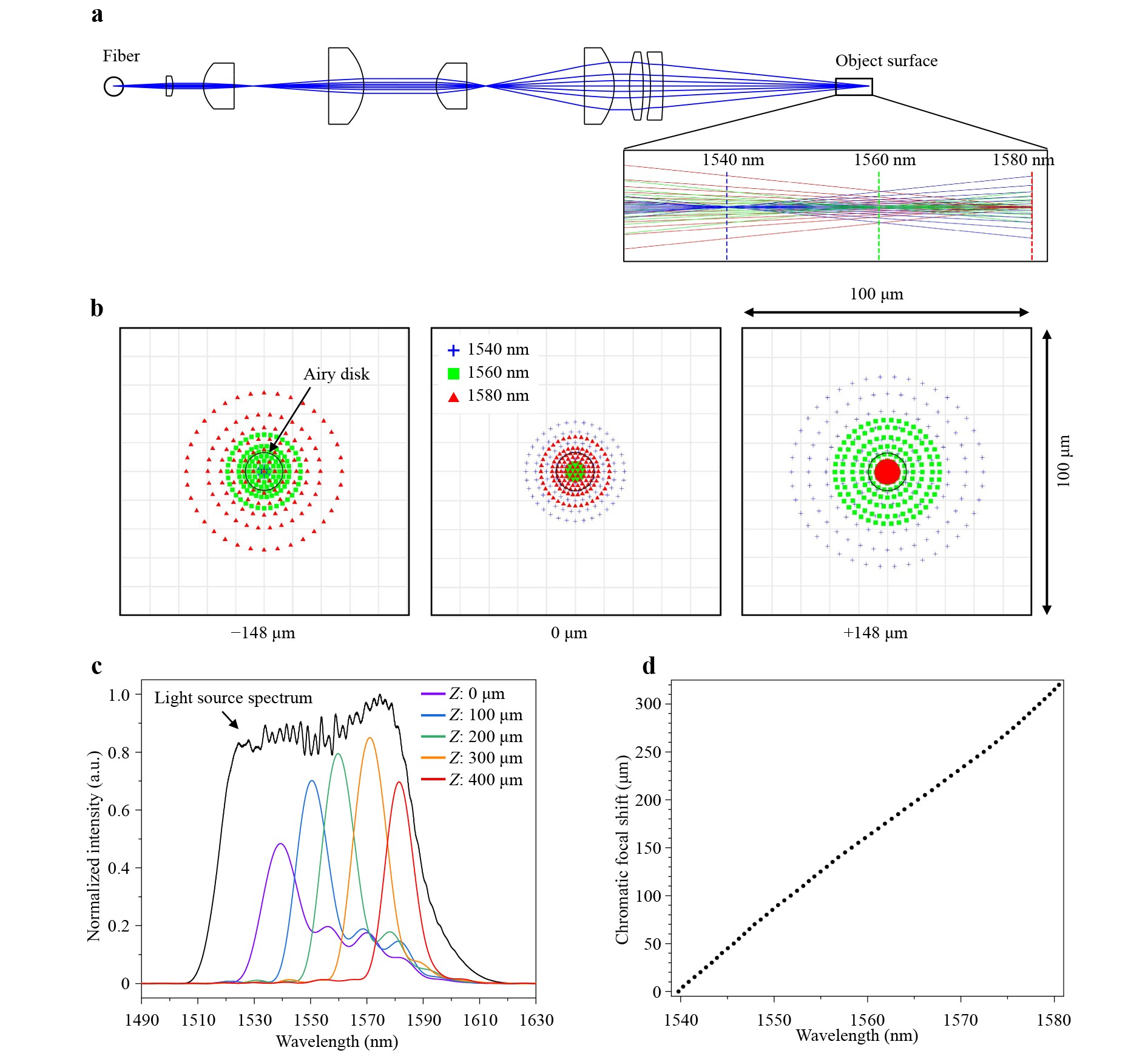
Fig. 2 IR chromatic confocal sensor design and performance. a Structure of the designed IR chromatic confocal optical sensor. An axial chromatic focal shift is observed within the 1540–1580 nm wavelength range. b Performance analysis of the designed IR chromatic confocal sensor. The axial chromatic focal shift achieves 296 μm over a 40 nm wavelength span with diffraction-limited performance. c Experimental results of IR chromatic confocal sensor on the mirror surface. Spectrum of light source (black) and each reflected signal within a 400-μm height range (100 μm step) is shown. d LUT relating wavelength to chromatic focal shift.
-
Fig. 3a-c show the measured spectra of wafers with thicknesses of 534.2 μm, 725.4 μm and 777.5 μm, respectively. In this study, 4-inch, 8-inch, and 12-inch silicon wafers, with typical thicknesses of approximately 525, 725 and 775 µm, respectively (±25 µm tolerance), were used to validate the system. As the IR chromatic confocal sensor does not include a separate reference arm, low-pass filtering the measured raw spectrum yields overlapping signals from the wafer’s top and bottom surfaces. The optical sensor was precisely focused such that the bottom-surface reflection in each wafer appeared at a center wavelength of 1581.36 nm ($ {\lambda }_{2} $). For the 534.2 µm wafer, the top-surface reflection occurred at 1562.95 nm ($ {\lambda }_{1} $), for the 725.4 µm wafer, it appeared at 1556.02 nm ($ {\lambda }_{3} $), and for the 777.5 µm wafer, it appeared at 1554.22 nm ($ {\lambda }_{4} $). The difference between the top and bottom center wavelengths was determined and converted to $ {d}_{conf} $ using the LUT. Because the relationship between wavelength and confocal focal shift is not perfectly linear (Fig. 2d), the LUT was constructed in 1 µm steps using a precision motorized stage, with linear interpolation employed for accuracy. This yielded $ {d}_{conf} $ values of 150.79 µm for the 534.2 µm wafer, 204.72 µm for the 725.4 µm wafer, and 219.38 µm for the 777.5 µm wafer. Note that, where the bottom reflection intensity was weak, the top reflection could dominate, distorting the bottom-center wavelength. In such cases, the top-surface contribution, obtained by low-pass filtering the mirror-measured spectrum centered at λ1, was subtracted from the low-pass-filtered wafer measurement spectrum, which contains a superposition of reflections, to isolate the bottom surface signal centered at λ2. Fig. 3d shows the unwrapped interference signal for both wafers, removing multiple internal reflections. To find the refractive index at λ2, the slope at 1.896 × 10¹⁴ Hz, corresponding to the frequency of λ2, from the unwrapped data was extracted. The final parameter needed, NA of the optical system, was determined through simulation, yielding 0.131. Note that, as required by Eq. 3 and as demonstrated in previous studies35, an accurate value of the sensor’s NA is essential for reliable thickness calculation. In our system, the NA was determined through optical simulation while accounting for vignetting and assembly tolerances, thereby minimizing NA-related errors. Over 20 repeated measurements, the thickness and refractive index at λ2 for the 534.2 µm wafer were 534.05 µm (repeatability of 72.3 nm) and 3.514; those for the 725.4 µm wafer were 725.09 µm (repeatability of 98.0 nm) and 3.512; and those for the 777.5 µm wafer were 777.15 µm (repeatability of 102.0 nm) and 3.514 respectively (Fig. 3e). Detailed explanations of the chromatic confocal signal analysis and the interference signal analysis process in the chromatic confocal spectral interferometry method are provided in Fig. S3 and Fig. S4 of Supplementary Information, respectively.
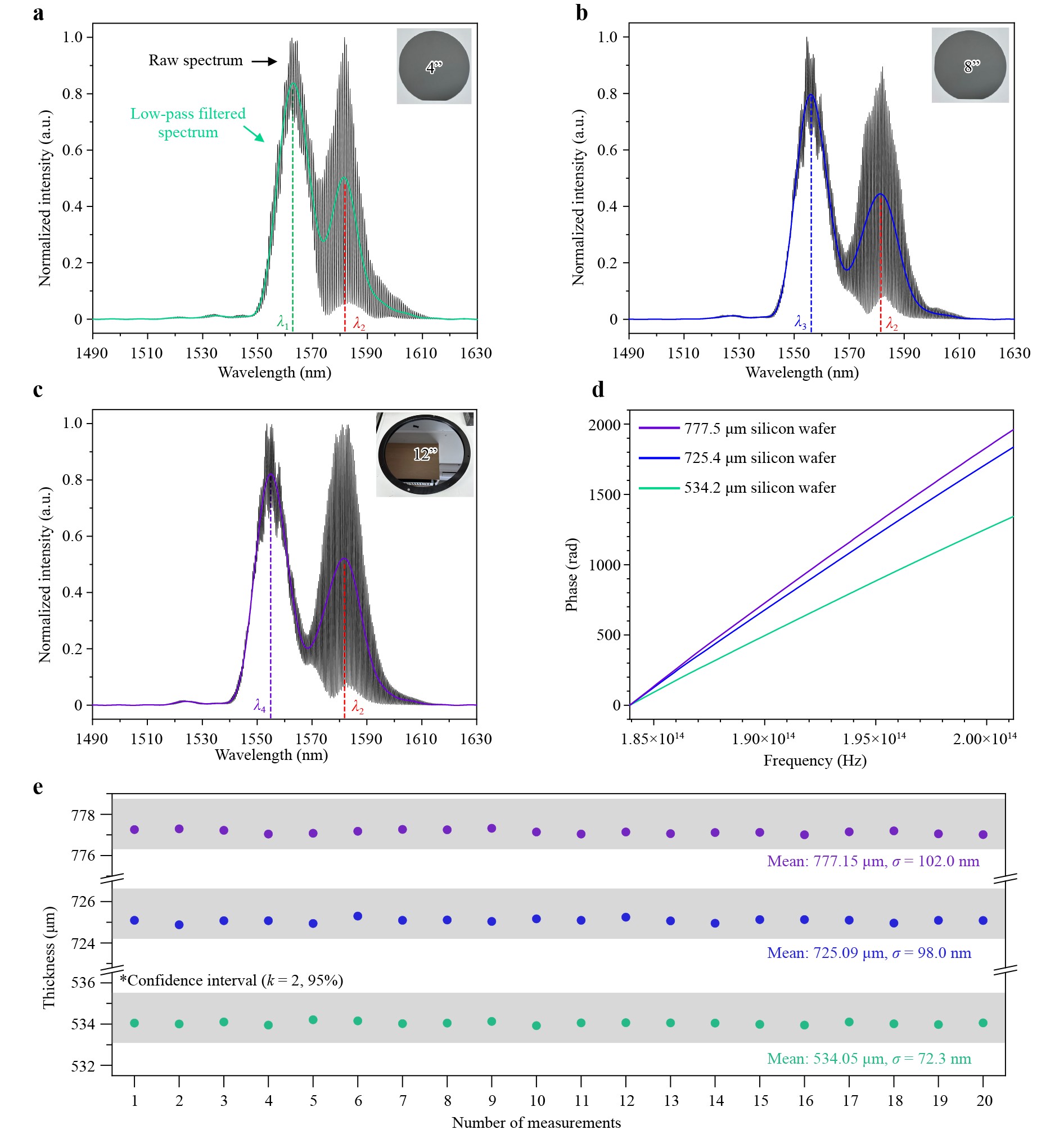
Fig. 3 Silicon wafer thickness measurement results. a Measured spectrum of wafer with a thickness of 534.2 μm. The raw spectrum (black) obtained from the OSA is processed with low-pass filtering (blue) to identify the center wavelengths of the signals reflected from the top ($ {\lambda }_{1}) $ and bottom ($ {\lambda }_{2}) $ surfaces. b Measured spectrum of wafer with a thickness of 725.4 μm. The center wavelength of the signal reflected from the top surface is $ {\lambda }_{3} $, and the center wavelength of the signal reflected from the bottom surface is $ {\lambda }_{2} $. c Measured spectrum of wafer with a thickness of 777.5 μm. The centre wavelength of the signal reflected from the top surface is $ {\lambda }_{4} $, and the center wavelength of the signal reflected from the bottom surface is $ {\lambda }_{2} $. d Unwrapped interference signals (phase versus frequency) for 534.2 μm, 725.4 μm, and 777.5 μm wafers. e Thickness measurement results for 534.2 μm, 725.4 μm, and 777.5 μm wafers. For the 534.2 µm wafer, the measured thickness is 534.05 µm with a repeatability of 72.3 nm, for the 725.4 µm wafer, the measured thickness is 725.09 µm with a repeatability of 98.0 nm, and for the 777.5 µm wafer, the measured thickness is 777.15 µm with a repeatability of 102.0 nm.
Table 1 lists the uncertainty analysis for IR chromatic confocal spectral interferometry using a 534.2 µm wafer ($ {L}_{1}) $, with an optical system total length including the focal length of the chromatic confocal sensor ($ {L}_{0}) $ of 232 mm and a refractive index (n) of 3.514. Uncertainty related to refractive index37 is given by 3.0 × 10⁻⁸, and the other uncertainty values were obtained from the measurements and analysis conducted in our previous research38. Since this hybrid method combines chromatic confocal and spectral interferometry, a systematic uncertainty evaluation was performed for each technique, and the results were then combined using Eq. 5 in the Methods section. The combined uncertainty of the entire system is 560.7 nm for the 534.2 µm silicon wafer. The thickness difference between measurements using IR chromatic confocal spectral interferometry and a surface profiler is 180 nm, within the uncertainty. Similarly, for the 725.4 µm and 777.5 µm wafers, the results show combined uncertainties of 563.3 nm and 565.4 nm (Table S1, Table S2), with corresponding thickness deviations of 320 nm and 340 nm, respectively, both of which remain within the estimated uncertainty bounds (Fig. 3e). Note that, the discrepancy between relative measurement error and relative uncertainty arises primarily from the dominant contribution of the chromatic confocal channel (12.4 times larger than that of the interferometric contribution) in the combined uncertainty budget. Due to the use of linear interpolation in the look-up table (LUT) with 1-µm stage increments, a thickness-independent error of approximately 100–200 nm is introduced. It is also important to note that measurement error and uncertainty characterize fundamentally different aspects of measurement and are not expected to scale in the same manner. Uncertainty reflects the statistical confidence based on the system model, whereas measurement error quantifies the actual deviation observed in a specific measurement. Therefore, even though the absolute error increases with thickness, it remains well within the estimated uncertainty bounds, validating the robustness of the uncertainty model. The chromatic confocal spectral interferometry method demonstrates a confidence level of approximately ±0.21% (k = 2, 95%) for the 534.2 µm wafer, which is well within the ±1.5-3% control range generally required to ensure reliable electrical connectivity in TSV depth39. Furthermore, the uncertainty associated with the refractive index measurement in chromatic confocal spectral interferometry is also analyzed in Table S3. Based on sensitivity coefficients, $ \left|{\partial n}/{{\partial }_{int}}\right|=9.36\times {10}^{-7} $, $ \left|{\partial n}/{{\partial }_{conf}}\right|=1.16\times {10}^{-5} $, the combined uncertainty in the refractive index is calculated to be 0.00367 (k = 1).
Source of uncertainty errors Value Value (nm) for L0 = 232 mm
L1 = 534.2 μm and n = 3.514① Systematic uncertainty of the interferometry $ \sqrt{{{②}}^{2}+{{③}}^{2}+{{④}}^{2}} $ 352.7 ② Uncertainty of DFT algorithm (L1·n) 352.4 nm ③ Uncertainty of OSA (0.01 nm) 6.6 × 10⁻⁶·L1·n ④ Uncertainty related to refractive index of air 3.0 × 10⁻⁸·L0 ⑤ Statistical uncertainty analysis of the interferometry $ \sqrt{{{⑥}}^{2}} $ 54.1 ⑥ Measurement repeatability of the interferometry 54.1 nm ⓐ Combined uncertainty of the interferometry ⓐ = $ \sqrt{{\text{①}}^{2}+{{⑤}}^{2}} $ 356.8 ⑦ Systematic uncertainty of the chromatic confocal $ \sqrt{{{⑧}}^{2}+{{⑨}}^{2}+{{⑩}}^{2}+{\text{⑪}}^{2}} $ 298.3 ⑧ Uncertainty of LUT (OSA: 0.04nm/step) 296 nm ⑨ Uncertainty of motor stage movement $ 2.0\cdot {10}^{-5}\cdot \dfrac{{L}_{1}}{n} $ ⑩ Uncertainty of calibration mirror flatness 36 nm ⑪ Uncertainty of refractive index of air 3.0 × 10⁻⁸·L0 ⑫ Statistical uncertainty analysis of the chromatic confocal $ \sqrt{{\text{⑬}}^{2}} $ 95.8 ⑬ Measurement repeatability of the chromatic confocal 95.8 nm ⓑ Combined uncertainty of the chromatic confocal ⓑ = $ \sqrt{{\text{⑦}}^{2}+{\text{⑫}}^{2}} $ 313.3 ⓒ Combined uncertainty of the chromatic confocal interferometry ⓒ = $ \sqrt{{\left(\dfrac{\partial t}{{\partial }_{int}}\text{ⓐ}\right)}^{2}+{\left(\dfrac{\partial t}{{\partial }_{conf}}{\text{ⓑ}}\right)}^{2}} $ 556.7 ⑭ Uncertainty of silicon wafer flatness 66.5 66.5 ⑮ Uncertainty related to the thermal expansion of silicon wafer 5.7 × 10⁻⁸·L1 0.03 ⓓ Combined uncertainty ⓓ = $ \sqrt{{\text{ⓒ}}^{2}+{\text{⑭}}^{2}+{\text{⑮}}^{2}} $ 560.7 Table 1. Uncertainty analysis of the IR chromatic confocal spectral interferometry for the 534.2 μm silicon wafer
The depth profiles of multiple holes etched in a silicon wafer were measured from the backside using IR chromatic confocal spectral interferometry. (Fig. 4). The spot size of the sensor in air, measured by a beam profiler, had a full width at half maximum (FWHM) of ~14 µm over the measurement range. A 200 µm-diameter hole, much larger than the beam size, was tested, and the sample was monitored from the backside using an InGaAs area sensor and a telecentric lens (Fig. 4a). A 2D contour analysis confirmed the 200 µm-hole diameter to match the lithography design. Measuring from the top surface can make the bottom diameter indiscernible due to weak return signals. However, backside inspection allows accurate determination of the bottom-hole diameter using the pixel size and system magnification (see Methods section). Note that the bottom of the etched hole scatters light strongly, reducing reflection intensity in certain regions; in the backside 2D image, the edges of the hole appeared darker than the center, likely due to black silicon or similar formations from the etching process. As a result, at some points along the hole edge, it was difficult to identify the center wavelength of the reflected bottom-surface signal, leading to significant measurement errors. To address this, the refractive index was first measured in adjacent hole-free areas with stronger bottom-surface signals. Using this refractive index, the hole depth was then computed by dividing the optical path from the interferometry data. By laterally scanning with 1-µm steps, the three 200-µm holes were found to have an average depth of 143.6 µm at their centers. Note that near the hole edge, interference signals from both the substrate and the hole bottom were detected simultaneously, and the stronger signal was selected for analysis. Since the reflection from the hole bottom is relatively weak due to surface scattering, this can lead to an underestimation of the hole’s actual diameter. To address this, it is important to use an area InGaAs sensor-based backside imaging system, as shown in Fig. 4a, to accurately determine the true hole diameter.
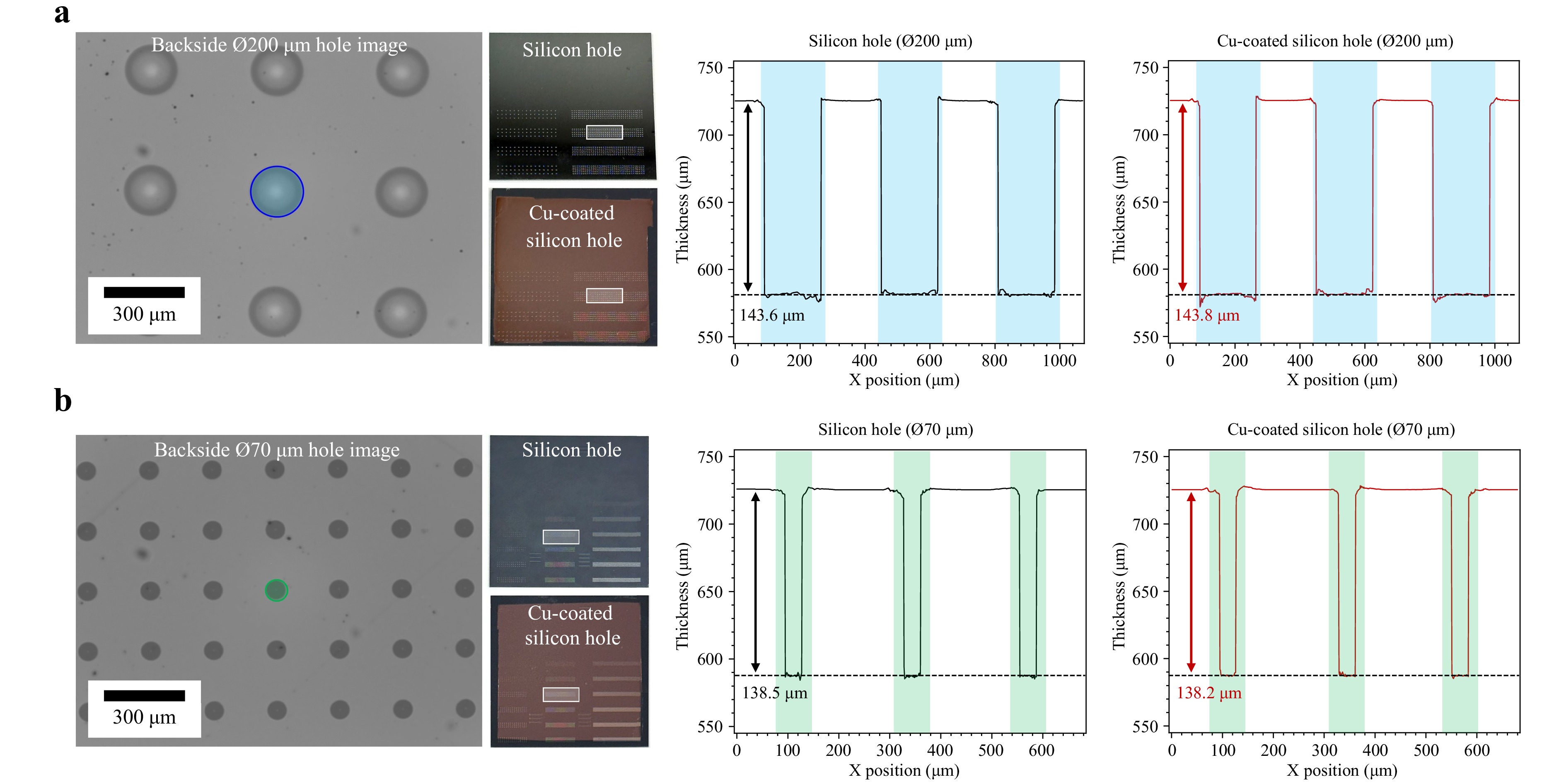
Fig. 4 Silicon sample hole depth profiling results. a The backside 2D image and hole depth profile results of a 200 µm-diameter hole. Contour analysis based on 2D images determines the hole diameter to be 200 µm (blue circle). The average depth is measured as 143.6 µm at the center of the bare silicon hole and 143.8 µm at the center of the Cu-coated silicon hole. b The backside 2D image and hole depth profile results of a 70 µm-diameter hole. Contour analysis based on 2D images determines the hole diameter to be 70 µm (blue circle). The average depth is measured as 138.5 µm at the center of the bare silicon hole and 138.2 µm at the center of the Cu-coated silicon hole.
In semiconductor devices, holes are typically filled with Cu to function as electrodes. When illuminated from the backside, the reflection interface transitions from silicon to a metallic surface. To reproduce these conditions for experimental validation, a silicon sample was prepared with a 150 nm-thick Cu layer deposited at the hole bottom. Since this thickness significantly exceeds the penetration depth of IR light in Cu, which is only a few nanometers, it can be reasonably assumed that all incident light at the hole bottom is fully reflected by the metal surface. Attributed to the higher reflectivity of the metal surface compared to silicon, the bottom-surface signal exhibited a higher SNR, and the three 200-µm holes were measured to have an average depth of 143.8 µm at their centers. The measurement was repeated on smaller 70 µm-diameter holes using the same method, yielding an average depth of 138.5 µm at the hole center in the silicon sample and 138.2 µm in the Cu-coated silicon sample (Fig. 4b). As shown in the complete silicon sample fabrication procedure in Fig. S5, the Cu-coated and bare silicon samples were patterned at different locations on the same 8-inch wafer, which can lead to depth variations due to position-dependent etching non-uniformity. Due to the relatively low NA of the implemented chromatic confocal sensor, measuring holes smaller than the beam spot size was challenging. The primary issues were the low SNR from the bottom surface and interference between the hole and substrate surfaces. To determine whether a higher NA could provide sufficient signal for holes with diameters below 10 µm, we employed a high-NA lens in a spectral interferometry setup. Measurements were then conducted on Cu-filled TSVs in a commercially fabricated memory chip to validate the approach.
-
The IR spectral interferometry system, developed with a high-NA objective lens and a beam-size-adjustable collimator, was used for demonstrating backside depth measurements of single Cu-filled TSVs and TSV arrays with diameters less than 10 µm (Fig. 5a). For a single Cu-filled TSV, the collimated beam size was reduced to lower the object NA, thereby increasing the Rayleigh length and creating a narrower spot at the Cu pillar bottom. With the object NA set to 0.28, the measured spot size at the pillar bottom was about 15 µm. For Cu-filled TSV arrays, the collimating beam size was increased to maximize the object NA. A larger NA decreases the Rayleigh length, creating a larger beam spot at the Cu pillar bottom. Adjusting the beam to fill the objective lens entrance pupil resulted in an object NA of 0.65 and a spot size of approximately 96 µm at the TSV array bottom. The spot size of the beam at the silicon bottom surface is larger than the TSV diameter, allowing the light to be reflected back from both the TSV hole bottom and the underlying silicon wafer surface. The optical simulation results for the TSV measurement setup are provided in Fig. S6. Fig. 5b shows representative spectra: Spectrum (i) corresponds to a region without a TSV, whereas Spectrum (ii) includes a low-frequency component from the TSV region. Fourier-transforming Spectrum (ii) yields three peaks: Peak (ⅲ) indicates interference between the sample bottom and TSV bottom, Peak (ⅳ) between the TSV bottom and the sample top, and Peak (ⅴ) between the sample top and bottom surfaces. This interpretation is confirmed by verifying that the time at Peak (ⅲ) equals the difference in times of Peaks (ⅳ) and (ⅴ). The Fourier transform of Spectrum (i) yields a single peak: Peak (ⅵ) indicates interference between the sample’s top and bottom, identical to Peak (ⅴ). These results further validate that Peaks (ⅲ) and (iv) arise from the TSV structure. Note that, the interference signal corresponding to Peak (iv) is robust against low-frequency noise, which arises from both source-induced fluctuations and reflections associated with micro-patterned structures on the backside surface, as it originates from a large optical path difference between the silicon surface and the TSV bottom. Moreover, a comparison of reflection spectra from Cu-filled and bare silicon holes is provided in Fig. S7, both of which yield well-defined signals suitable for analysis. Since the measured signal corresponds to the optical thickness, the physical TSV depth is obtained by dividing it by the group refractive index (3.586). This group index was obtained by dividing the optical thickness (measured with a parallel beam) to the physical thickness of the substrate, which was measured using a high-precision surface profiler. Note that, the group index (3.586) is larger than the earlier phase index values due to dispersion, as it is based on group delay rather than phase delay. After accounting for the optical system NA via a scaling factor, the TSV depth was accurately determined. Over 20 consecutive measurements for each of the 10 adjacent Cu-filled TSVs revealed a depth repeatability of 18.7 nm and a 172 nm deviation from the target (Fig. 5c), which is acceptable given the variability in TSV etch depth across a 12-inch wafer26,40,41, marking the first successful demonstration of backside depth measurement for Cu-filled TSVs otherwise inaccessible from the front. Table 2 lists the uncertainty analysis of the adjustable NA sensor-based spectral interferometry for a TSV with a 50-μm depth (L1), where the optical system has a total length of 118 mm (L0), including the focal length of the high-NA objective lens, yielding a combined uncertainty of 37.8 nm and a total of 76.5 nm when considering silicon flatness and thermal expansion. The dominant contributor, silicon wafer flatness, stems from the sample fabrication process rather than the measurement system, and can be mitigated to 20 nm level through double-sided CMP42. Fig. 5d shows the depth measurements of the Cu-filled TSV array from the upper, center, and lower sections of five 12-inch wafers, all defined on the same plane, with three zones measured per region. Across all samples, the maximum deviation from the target depth was 334 nm, within the process- and environment-related uncertainty range, thereby confirming the reliability of these measurements.
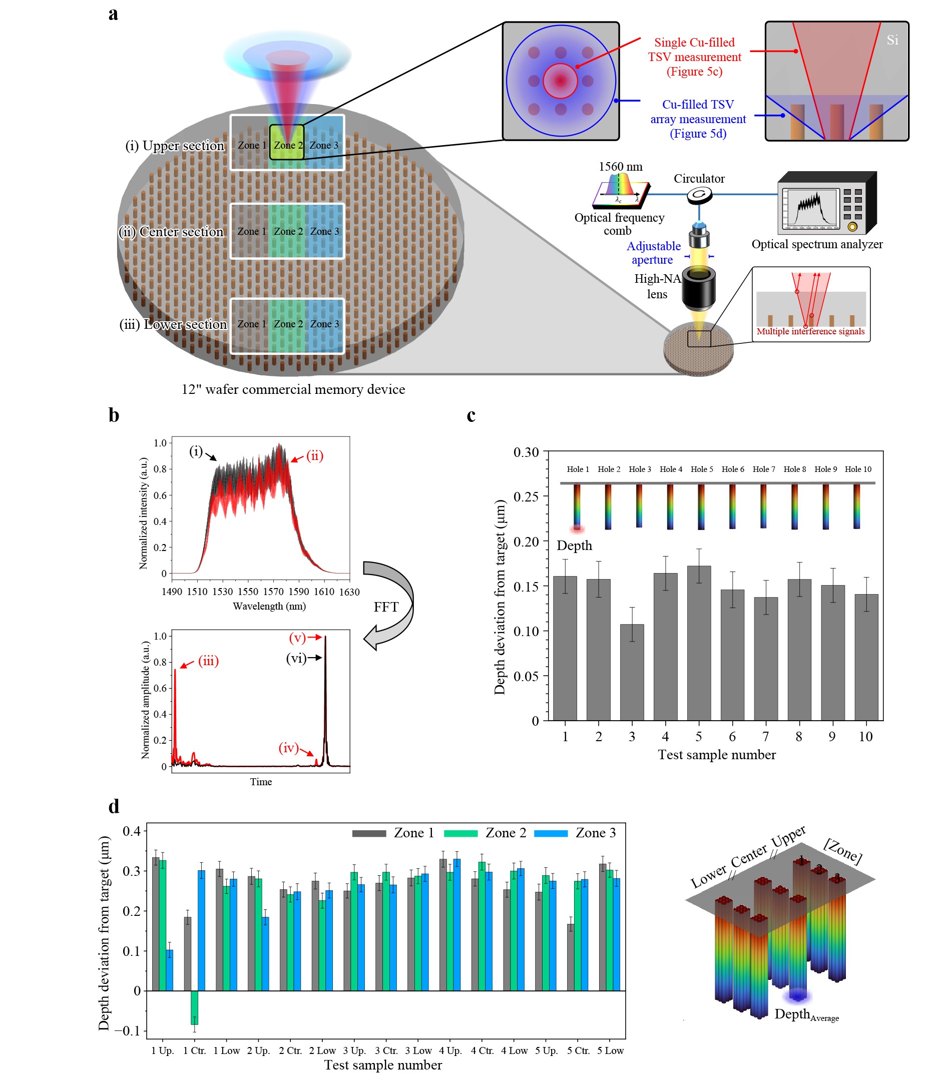
Fig. 5 Cu-filled TSV depth measurement results. a Operation principle and experimental setup of spectral interferometry with a high-NA lens for measuring a commercial memory device in a 12-inch silicon wafer. b Measured optical spectra with and without the TSV ((ii) and (i) respectively), along with their corresponding FFT results. Peaks (ⅲ), (ⅳ), and (ⅴ) indicate interference between the sample bottom and TSV bottom, the TSV bottom and sample top, and the sample top and bottom surfaces, respectively. Peak (ⅵ) indicates interference between the sample top and bottom surfaces in the case without TSV. c Depth measurement results of a single Cu-filled TSV. The measured depth has a deviation of 172 nm, with a repeatability of 18.7 nm. d Depth measurement results of Cu-filled TSV arrays across five 12-inch wafers. The measurements are performed at the upper, center, and lower sections of each wafer, with three zones measured per region. The maximum deviation from the target depth is 334 nm.
Source of uncertainty errors Value Value (nm) for L0 = 118 mm
L1 = 50 μm and N = 3.586① Systematic uncertainty of the interferometry $ \sqrt{{{②}}^{2}+{{③}}^{2}+{{④}}^{2}} $ 32.9 ② Uncertainty of DFT algorithm (L1·N) 32.7 nm ③ Uncertainty of OSA (0.01 nm) 6.6 × 10⁻⁶·L1·N ④ Uncertainty related to refractive index of air 3.0 × 10⁻⁸·L0 ⑤ Statistical uncertainty analysis of the interferometry $ \sqrt{{{⑥}}^{2}} $ 18.7 ⑥ Measurement repeatability of the interferometry 18.7 nm ⓐ Combined uncertainty of the interferometry ⓐ = $ \sqrt{{{①}}^{2}+{{⑤}}^{2}} $ 37.8 ⑦ Uncertainty of silicon wafer flatness 66.5 66.5 ⑧ Uncertainty related to the thermal expansion of silicon wafer 5.7·10−8·L1 0.003 ⓑ Combined uncertainty ⓑ = $ \sqrt{{\text{ⓐ}}^{2}+{{⑦}}^{2}+{{⑧}}^{2}} $ 76.5 Table 2. Uncertainty analysis of the IR chromatic confocal spectral interferometry for the 534.2 μm silicon wafer
-
By combining chromatic confocal microscopy and spectral interferometry with an optical frequency comb centred at 1560 nm, which can penetrate silicon, we demonstrated a backside measurement technique that simultaneously determines both the thickness and refractive index of silicon with high spatial resolution. Without requiring Z-axis scanning, silicon samples with thicknesses of several hundred micrometres, commonly used in semiconductor processes, were measured with a spatial resolution of ~14 µm and a repeatability of 72.3 nm for the 534.2 μm silicon wafer. Moreover, by utilizing a high-NA lens in combination with spectral interferometry, we were able to measure the depth of both individual Cu-filled TSVs and TSV arrays under varying NA conditions. This study represents the first successful demonstration of measuring the depths of Cu-filled single TSVs and TSV arrays from the backside, specifically designed for commercial memory products. Note that, while this study employed a chromatic confocal sensor combined with commercial lenses, resulting in a relatively low NA of approximately 0.131, the TSV measurement results suggest that utilizing a custom chromatic confocal sensor with an NA exceeding 0.3 will enable depth measurements of TSVs with diameters less than 10 µm. Also, as TSV depths increase and diameters decrease in future applications, this backside illumination-enabled metrology maintains a high SNR from the backside, ensuring reliable measurement performance. Note that, in the presence of a backside dielectric layer, TSV depth can be directly measured using high-NA spectral interferometry, as the dielectric-induced phase delay is common to both reference and signal paths and thus cancels out. For the chromatic confocal spectral interferometry, it requires compensation by incorporating the optical path length of the dielectric layer, determined from its physical thickness and refractive index, to ensure accurate depth retrieval.
The optical frequency comb used in our system provides several key advantages over conventional broadband sources. Most notably, it offers exceptionally low residual intensity noise (–150 dBc/Hz at 10 MHz offset)43,44, enabling superior signal-to-noise ratio (SNR) and robust FFT peak detection in noise-sensitive measurements such as backside wafer metrology. Resolving thick silicon wafers at 1550 nm, where dispersion is weak, requires broad spectral bandwidth; a 70-nm frequency comb used in this work provided both the bandwidth and power needed for accurate chromatic confocal sensing. In terms of scalability, frequency combs offer compelling potential: ultra-broadband spectra exceeding 450 nm have been demonstrated45, enabling improved axial resolution, and advanced acquisition methods such as photonic time-stretching method can achieve acquisition rates beyond 100 MHz46 – far exceeding conventional spectrometer-based systems. Notably, Er-doped fiber combs are becoming increasingly affordable and robust, with recent turnkey systems now available. While the Er-fiber comb was used in this work for performance benchmarking, more economical alternatives such as electro-optic (EO) combs or superluminescent diodes (SLDs) remain viable for less demanding applications, offering flexible cost-performance trade-offs.
Currently, the total measurement time per point in the system is approximately 0.8 seconds, comprising ~0.5 seconds for optical spectrum acquisition using an OSA and ~0.3 seconds for signal processing performed in MATLAB. This corresponds to a throughput of approximately 75 points per minute, excluding stage translation time. Note that, in contrast to conventional methods that rely on mechanical Z-axis scanning34, our method achieves one-shot measurements without mechanical motion, significantly improving throughput. Although the current setup prioritizes precision validation using commercial instruments, future implementations may achieve even faster acquisition by replacing the OSA with a wavelength-dispersive detection system (e.g., diffraction grating and line-scan camera47) and optimizing processing algorithms for real-time operation48.
In addition, by incorporating reference arms into the sensor to analyse interference signals from the sample’s reflections, it becomes possible to measure not only the thickness of silicon wafers but also their geometric thickness, thereby enabling the evaluation of wafer warpage49, an increasingly critical factor in advanced packaging that impacts yield in semiconductor fabrication processes. To apply this approach to the proposed system, careful dispersion matching would be required, as the chromatic confocal lens in the sample arm introduces intentional dispersion that must be compensated to preserve interference signal integrity.
A performance comparison between chromatic confocal spectral interferometry and alternative techniques, including IR spectral interferometry and industrial X-ray computed tomography, is presented in Table S4 of Supplementary Information, demonstrating that the proposed chromatic confocal spectral interferometry is well-suited for in-line inspection owing to its superior precision and fast acquisition speed.
-
An optical frequency comb (FC1500-250-ULN, Menlo Systems) centred at 1560 nm with a 70 nm optical bandwidth at -3 dB, generated by a 250 MHz mode-locked erbium-doped fibre oscillator, was used as a light source. Applying optical pulses with an average power of ~35 mW to the IR chromatic confocal sensor through a circulator, ~0.8 mW of reflected light is collected from the mirror. The target is scanned along the 3-axis directions using a precision motor stage (±100 nm repeatability). The signal reflected from the target is analysed using an OSA (MS9710C, Anritsu) with a 200 nm optical span and a wavelength resolution of 0.04 nm.
-
The design wavelength range was set to 1540–1580 nm, where the optical frequency comb shows a relatively flat spectrum. To achieve an axial chromatic focal shift of ~300 µm over a 40 nm wavelength bandwidth, sufficient for measuring silicon wafers with thicknesses of several hundred micrometers, seven glass lenses made of N-BK7, N-SF6, and D-ZK3M materials were optimized in Zemax OpticStudio software. Multiple aspheric lenses were employed to minimize optical aberrations other than axial chromatic aberration. In a chromatic confocal system, a high object NA is required to narrow the optical bandwidth of the reflected signal. Diverging light from a polarization-maintaining single-mode fiber (10 µm core, NA = 0.14) was collimated and then expanded via a two-stage beam expander to match the entrance pupil of the focusing lens, thereby achieving the desired object NA. After considering mechanical constraints such as the retainer ring and lens barrel in the sensor, the system achieves an object NA of 0.131.
-
To simultaneously determine the thickness and refractive index of a medium, measurement results from both chromatic confocal sensing (which underestimates the thickness) and spectral interferometry (which overestimates the thickness) are combined. The chromatic confocal thickness50 ($ {d}_{conf} $), defined as the distance difference between the signals reflected from the upper and lower surfaces of the transparent sample, is derived from Eq. 1 as follows:
$$ {d}_{conf}=t\times \frac{{n}_{1}\left(\nu \right)}{{n}_{2}\left(\nu \right)}\times \dfrac{{\left[1-{\left(\dfrac{NA}{{n}_{1}\left(\nu \right)}\right)}^{2}\right]}^{1/2}}{{\left[1-{\left(\dfrac{NA}{{n}_{2}\left(\nu \right)}\right)}^{2}\right]}^{1/2}} $$ (1) where t is the sample thickness, $ {n}_{1} $ is the refractive index of air, $ {n}_{2} $ is the refractive index of the sample, and NA is the object numerical aperture of the sensor. The optical thickness51 ($ {d}_{int}) $, which is the product of the geometrical thickness and the refractive index, is derived from Eq. 2 as follows:
$$ {d}_{int}={t\times n}_{2}\left(\nu \right)=\frac{c}{4\pi }\times \frac{d\phi \left(\nu \right)}{d\nu } $$ (2) where c is the speed of light and $ \phi $ is the phase of the interference signal. By combining the equations for chromatic confocal thickness and optical thickness, the physical thickness35 of the sample is derived from Eq. 3 as follows:
$$ t={\left[\frac{{NA}^{2}{d}_{conf}^{2}-{\left\{{NA}^{4}{d}_{conf}^{4}+4(1-{NA}^{2}){d}_{int}^{2}{d}_{conf}^{2}\right\}}^{1/2}}{-2(1-{NA}^{2})}\right]}^{1/2} $$ (3) Refractive index is also derived from combining the equations for chromatic confocal thickness and optical thickness as follow:
$$ n=\sqrt{\frac{{NA}^{2}+\sqrt{{NA}^{4}+4{\left(\dfrac{{d}_{int}}{{d}_{conf}}\right)}^{2}(1-{NA}^{2})}}{2}} $$ (4) -
Since $ {d}_{int} $ and $ {d}_{conf} $ are independent and uncorrelated, the combined standard uncertainty52 is derived from Eq. 5 as follows:
$$ u\left(t\right)=\sqrt{{\left(\frac{\text{∂t}}{\text{∂}{\mathrm{d}}_{\mathrm{i}\mathrm{n}\mathrm{t}}}\cdot u\left({d}_{int}\right)\right)}^{2}+{\left(\frac{\text{∂t}}{\text{∂}{\mathrm{d}}_{\mathrm{c}\mathrm{o}\mathrm{n}\mathrm{f}}}\cdot u\left({d}_{conf}\right)\right)}^{2}} $$ (5) where ${\text{∂t}}/{\text{∂}}{\mathrm{d}}_{\mathrm{i}\mathrm{n}\mathrm{t}} $ and ${\text{∂t}}/{\text{∂}{\mathrm{d}}_{\mathrm{c}\mathrm{o}\mathrm{n}\mathrm{f}}} $ are the sensitivity coefficients of the interferometric and chromatic confocal measurements, and $ u\left({d}_{int}\right) $ and $ u\left({d}_{conf}\right) $ are the uncertainties associated with the interferometric and chromatic confocal, respectively. For the 534.2 µm wafer measurement ($ {d}_{conf} $ = 150.79 µm, $ {d}_{int} $ = 1876.45 µm, t = 534.05 µm), the sensitivity coefficients $ {\text{∂t}}/{\text{∂}{\mathrm{d}}_{\mathrm{i}\mathrm{n}\mathrm{t}}} $ and $ {\text{∂t}}/{\text{∂}{\mathrm{d}}_{\mathrm{c}\mathrm{o}\mathrm{n}\mathrm{f}}} $ were calculated to be 0.1424 and 1.7696, respectively. The corresponding standard uncertainties $ u\left({d}_{int}\right) $ and $ u\left({d}_{conf}\right) $, as calculated in Table 1, were 356.8 nm and 313.3 nm, respectively. As a result, the combined uncertainty of the chromatic confocal interferometric measurement was estimated to be 556.7 nm.
-
To observe the patterned silicon sample from the backside, an imaging system equipped with an InGaAs sensor was developed. A camera covering a wavelength range of 400–1700 nm was utilized, with a resolution of 1280 × 1024 and a pixel size of 5 µm. Using a 4× magnification telecentric lens and a 1550 nm center-wavelength LED coaxial illumination, the pixel size in the inset image of Fig. 4 is 1.25 µm.
-
The IR chromatic confocal spectral interferometry setup was modified by replacing the IR chromatic confocal sensor with a high-NA objective lens with adjustable aperture. The beam size was adjusted before entering a 50× objective lens (NA = 0.7) to control the NA. Utilizing the full NA of 0.7 requires an input beam with a 5.68 mm entrance pupil diameter. For the low-NA setting, designed for measuring single Cu-filled TSVs, a 2.28 mm collimated beam resulted in an object NA of 0.28. For the high-NA setting, optimized for measuring Cu-filled TSV arrays, a 5.25 mm collimated beam yielded an object NA of 0.65. When optical pulses with an average power of ~35 mW are applied to the high-NA objective lens through a circulator, ~17 mW of reflected light is collected in the low-NA setting and ~12 mW in the high-NA setting.
-
Double side polished (DSP) wafers with thicknesses of 534.2 µm, 725.4 µm, and 777.5 µm were used as samples. The wafer thickness was measured using a precision surface profiler (Dektak 8, Bruker) with sub-nanometre resolution, and was found to be 534.23 µm, 725.41 µm and 777.49 µm, respectively. Next, a DRIE-patterned silicon sample was fabricated on a 725.4 µm wafer via lithography, DRIE, and photoresist removal. The depths of the holes in the fabricated silicon sample were measured using a commercial confocal microscope (LSM 980, ZEISS). These measurements revealed variations of 140–145 µm for 200 µm-diameter holes and 135–140 µm for 70 µm-diameter holes, which were attributed to variations in etching uniformity and measurement deviations caused by scattering from the surface. Finally, Cu-filled TSV samples, with a depth within the 30 to 50 µm range and hole diameters less than 10 µm, designed for use in commercial memory products, were provided by Samsung Electronics Co., Ltd.
-
This research was supported by the Industry-Academia Cooperation Program of Samsung Electronics Co., Ltd. (IO231013-07392-01) and the National Research Foundation (NRF) of Korea (Grants RS-2021-NR060086, RS-2024-00334727, RS-2024-00436737).
Backside illumination-enabled metrology and inspection inside 3D-ICs using frequency comb-based chromatic confocal and spectral interferometry
- Light: Advanced Manufacturing , Article number: (2025)
- Received: 07 April 2025
- Revised: 25 August 2025
- Accepted: 04 September 2025 Published online: 29 October 2025
doi: https://doi.org/10.37188/lam.2025.074
Abstract: Optical non-destructive inspection technologies are becoming increasingly crucial in semiconductor manufacturing to meet the growing demand for miniaturized, high-density, and integrated semiconductor devices. Conventional inspection techniques typically analyse semiconductor devices from the front side, but this approach poses challenges for highly integrated devices with micro and high-aspect-ratio structures due to scattering issues and low signal-to-noise ratios. Furthermore, it becomes impossible to measure the depth of Cu-filled through-silicon vias (TSVs) due to the low penetration depth of light in metals. Here, by combining chromatic confocal microscopy and spectral interferometry with an IR optical frequency comb centred at 1560 nm, which can penetrate silicon, we demonstrate a new backside silicon inspection technique. The demonstrated method is capable of simultaneously measuring thickness and refractive index with a high spatial resolution of ~14 μm and a repeatability of 72.3 nm for the 534.2 μm silicon wafer. We also conducted the first successful depth measurements of Cu-filled TSVs in commercial memory products using IR spectral interferometry with a high-numerical aperture (NA) lens, for both individual Cu-filled TSVs and TSV arrays under different NA conditions.
Research Summary
Seeing Through Silicon: Frequency Combs Enable Non-Destructive 3D Chip Inspection
As demand grows for faster and more energy-efficient computing, advanced 3D semiconductor devices require precise, non-destructive inspection. Researchers from the Korea Advanced Institute of Science and Technology (KAIST) and Samsung Electronics Co. Ltd., led by Professor Jungwon Kim of KAIST, has developed backside illumination-enabled metrology and inspection inside 3D-ICs using frequency comb-based chromatic confocal and spectral interferometry. By illuminating the wafer from the backside with infrared frequency comb, which penetrates silicon, this approach allows simultaneous measurement of both thickness and refractive index with high lateral resolution. The team demonstrated the technology on silicon wafers of multiple sizes and on commercial memory devices containing copper-filled TSVs, which conventional front-side inspection could not reliably measure. Adjusting optical parameters allowed both single-via and array inspection, showing versatility for real production environments.
Rights and permissions
Open Access This article is licensed under a Creative Commons Attribution 4.0 International License, which permits use, sharing, adaptation, distribution and reproduction in any medium or format, as long as you give appropriate credit to the original author(s) and the source, provide a link to the Creative Commons license, and indicate if changes were made. The images or other third party material in this article are included in the article′s Creative Commons license, unless indicated otherwise in a credit line to the material. If material is not included in the article′s Creative Commons license and your intended use is not permitted by statutory regulation or exceeds the permitted use, you will need to obtain permission directly from the copyright holder. To view a copy of this license, visit http://creativecommons.org/licenses/by/4.0/.

 DownLoad: