


-
Photothermal lithography has recently emerged as an attractive alternative to photochemical direct laser writing, which is commonly employed in the microfabrication industry1, 2. In photochemical laser writing, a focused laser beam (usually a UV or DUV laser) is scanned over a photoactive polymer, rendering it soluble (or insoluble) in certain developers/solvents3. Once developed, the “printed” pattern emerges and can be transferred to a substrate via wet or dry etching. On the other hand, in photothermal processing, a laser beam is incident on a heat-mode resist, permanently changing either its phase or its composition4. Once the state is changed, the patterned film also shows distinct etch selectivity against certain solvents, as well as certain dry etch chemistries. Similar to photopolymer-based processing, this enables pattern transfer of the laser-written film to the underlying substrate5. Although the achievable resolutions are in the hundreds of nanometers, falling short of the capabilities of the state-of-the-art high-NA EUV lithography tools, photothermal lithography development remains essential for technologies where sub-10 nm resolution is not required (e.g. semiconductor chip packaging, MEMS fabrication, automotive electronics, etc.).
Photothermal resists are generally classified into two main categories: organic resists, such as calixarene derivatives6, metal hydrazone complexes (MHC)7, and various polymeric materials8, 9; and inorganic resists, including metallic glasses10, metal oxide films11, and phase-change materials (PCMs)12, 13. Organic resists, which are widely used, often suffer from irregular edge contours and poorly defined pattern boundaries between exposed and unexposed regions. These limitations are primarily due to their high molecular weight, long organic molecular chains, broad thermal transition ranges, and thermal cross-linking effects. In contrast, inorganic resists typically offer higher resolution, producing well-defined, regular, and steep edge profiles after etching. These advantages arise from their lower molecular weight and narrower thermal transition ranges14. Among inorganic materials, SbTe-based PCMs are particularly promising as heat-mode resists, owing to their broad spectral response, obvious thermal threshold behavior, straightforward fabrication process, and low line-edge roughness15.
Photothermal lithography offers several advantages over photochemical lithography16. First, the process itself is not limited by the diffraction limit since it is sensitive to the temperature threshold rather than the laser dose, enabling resolutions well below the diffraction limit to be achieved17−19. Second, photothermal lithography makes the process more immune to beam scattering irrespective of exposure time, due to the dependence of PCMs on reaching the temperature threshold20. Third, photothermal resists are stable against unintentional exposure from ambient background radiation21. Fourth, thermal resists are generally grown via vacuum deposition instead of spin/spray coating, which enables uniform, controlled-thickness resist deposition on extremely small surfaces such as the tips of optical fibers22, 23. Fifth, due to the thermal nature of the patterning process, lasers do not need to operate in the UV/DUV regime in order to achieve the desired resolution, allowing greater flexibility in laser selection based on the application24.
While recent work has shown highly promising results, especially regarding the smallest features that could be written using phase-change lithography, the trend has always been to focus on “proof-of-concept” rather than core criteria that need to be addressed if the technique is to emerge as a viable alternative to traditional methods.
These criteria—including uniformity, repeatability, durability, yield, sidewall roughness, suitability for different substrates, as well as minimum achievable resolution and pitch25−27—remain underexplored or insufficiently optimized in much of the existing literature28, 29. In this work, we aim to address all these points and show that phase-change lithography is highly suitable for high-resolution, high-throughput processing for future applications.
-
One of the major challenges in phase-change lithography is the balance between resolution, film thickness, and optical power density30, 31. A continuous laser pulse with high optical power density would crystallize phase-change materials at large depths but compromise the pattern resolution, causing enlarged patterns as the heat dissipates laterally through the thin film32, 33. Since the phase-change crystallization is driven by field intensity rather than by energy (or dose), continuous laser pulses are not necessary. Sufficient optical absorption in the material, however, is necessary to cause the temperature increase, resulting in the nonlinear response between the optical intensity and the crystallization field. The crystallization temperature threshold varies based on phase-change material choice34−36. In this work, Germanium Antimony Telluride (Ge2Sb2Te5, GST) is used, which has a crystallization temperature threshold, Tth, of 175°C.
Fig. 1a shows the portion of a Gaussian pulse of 400 ns duration that would achieve the desired threshold temperature and beyond (Supplementary Information S.1). However, for visible or UV wavelength lasers—with which we can achieve a smaller spot size compared to NIR/IR wavelengths—the absorption depth of ~10−20 nm implies that thermal diffusion and wave propagation are necessary for thicker film crystallization. As diffusion proceeds isotropically, this creates a major challenge for maintaining the minimal spot size while achieving reasonable crystallization depths.
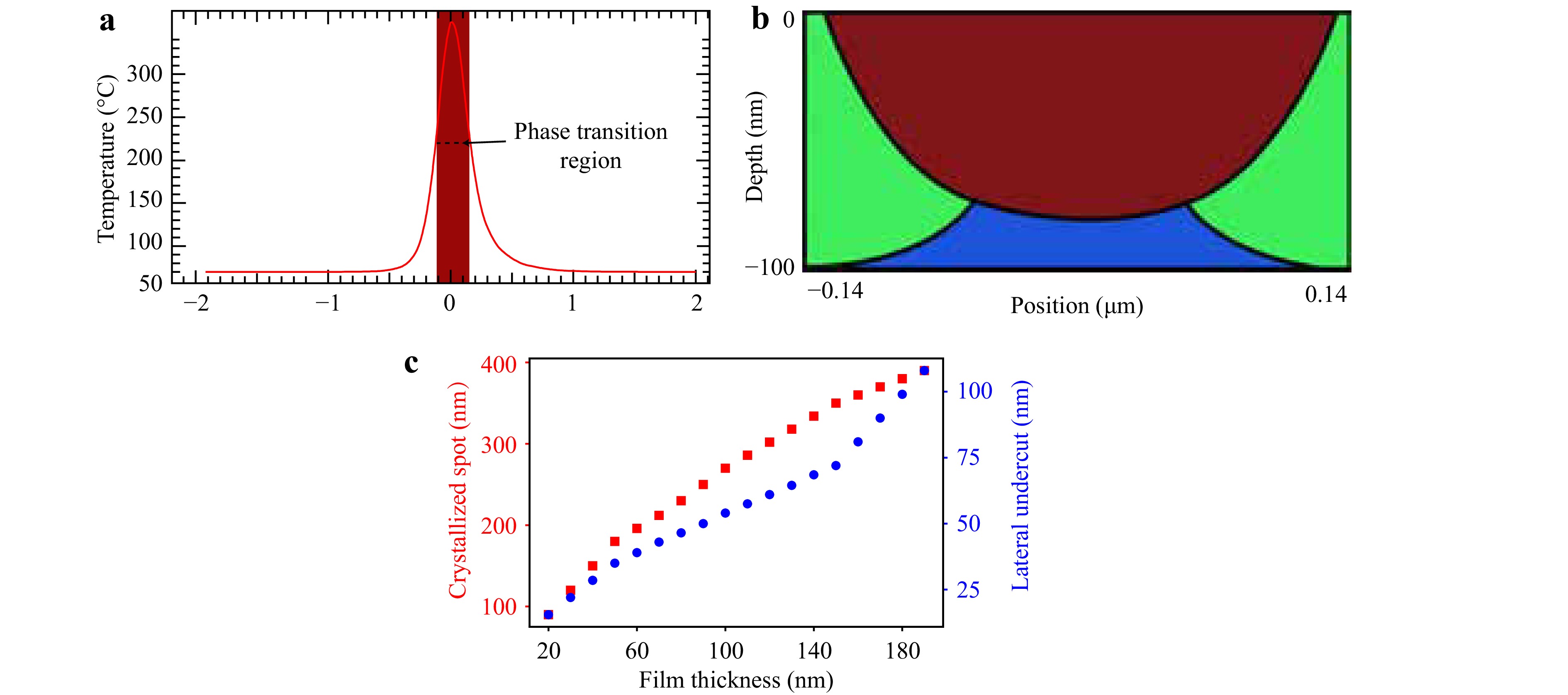
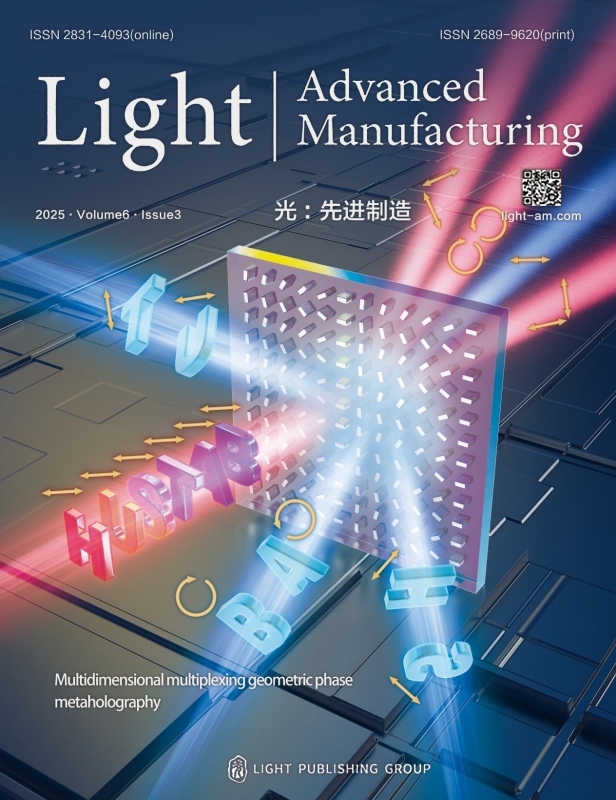
Fig. 1 a Temperature at the phase-change material surface with the red region showing the region above the crystallization phase transition threshold (175°C) indicating ~270 nm crystallized area. b Cross-sectional area of the region under the laser irradiation and wet etching; red - crystallized region; green - etched amorphous region; blue - unetched amorphous region. c Finite element method model of the optical absorption depth showing the lateral undercut of ~60 nm and the crystallization width at surface of ~270 nm for a ~100 nm Ge2Sb2Te5 thin film.
To better understand the thermal boundaries and process limitation of this thermal lithography technique, finite element methods are used to quantify the achievable patterns. A 532 nm optical pulse is used to model the absorption depth in a 100 nm GST thin film. Fig. 1b shows the thermal profile from the finite element model that includes the phase-change dynamics. The red region shows the crystallized spot, which clearly indicates that crystallization via thermal diffusion can achieve depths ~80 nm with a crystallization width of ~270 nm at the thin film surface. Assuming isotropic wet etching is employed to remove the amorphous region, this leads to a ~60 nm undercut from either side of the written region (green region in Fig. 1b). The blue region of the figure indicates amorphous regions that are unetched—assuming the etch is timed to stop once the substrate is reached. This figure shows how a judicious choice of pulse dynamics and etch timing leads to a stable structure with the highest resolution for a given film thickness.
To further illustrate this point, the achievable spot size and undercut due to the curved crystallization profile are plotted for film thicknesses ranging from 20 to 200 nm (Fig. 1c). In this simulation, the finite element model finds the smallest achievable feature for a given film thickness, such that the undercut does not exceed 25% of the crystallized spot size (or 50% of the half-width of the spot). This condition should ensure a stable structure for subsequent etching (wet or dry) of the sample and further downstream processing. Due to the limitation of the absorption depths of 532 nm wavelength in GST37, Fig. 1c depicts the resolution as a combination between the minimum achievable spot size (determined by the wavelength and diffraction limit) and the thermal diffusion/crystallization kinetics. Results confirm that the minimum achievable spot size is hence wider for thicker GST films. As discussed below, this matches well with our experimental findings.
Fig. 1 can be used as a guide to establish whether phase-change-based lithography yields a satisfactory resolution for a particular application, but must be complemented with extra information such as specific subsequent processing (pattern transfer or lift-off), device film and etch selectivity, presence of etch-stop layer, etc. (additional details in Supplementary Information S.2).
-
Photothermal lithography is a technique that uses optical power as a heat source to alter a photoresist. In this work, we use this method to pattern a hard mask directly on the surface of the sample using a GST thin film, a PCM that is robust and not photosensitive. Since PCMs are materials that produce a change in their physical state through thermal stimuli, we used optical power supplied by a 532 nm laser source to anneal the PCM above its phase transition temperature (i.e. 175°C) in order to pattern the hard mask38. The power density used in this work ranged from 5.9E+3 W/cm2 to 10.6E+3 W/cm2 with changes applied based on the PCM film thickness and optical power depth profile (additional details in Supplementary Information S.4).
-
The direct laser writing (DLW) optical setup is built using a 500 mW, 532 nm laser (CNI Laser) and a series of optical components designed to precisely control and deliver optical energy to the sample for PCM switching (Fig. 2). The laser beam is first polarization filtered and then directed through an Intraaction Corp acousto-optic modulator (AOM), which is controlled by a home-built pulse delay generator. This setup enables the generation of laser pulses with adjustable widths down to 200 ns and output power controllable up to 400 mW, allowing for localized heating and controlled switching of the GST thin film from amorphous to crystalline state minimizing lateral thermal dissipation. The beam is expanded to fill a 100X 1.3 NA oil immersion objective lens, which focuses the light onto the sample and helps reduce diffraction and improve resolution39. The polarization state of the beam entering the objective lens is controlled using an achromatic quarter-wave plate. The GST sample is mounted on top of a closed-loop piezoelectric stage that can be finely tuned using a tip-tilt micrometer stage. To enable real-time imaging during patterning, white light from a tungsten-halogen lamp is collimated and directed through a beam splitter to a co-focusing objective, allowing direct visualization of the patterning process in real time via a CMOS image sensor.
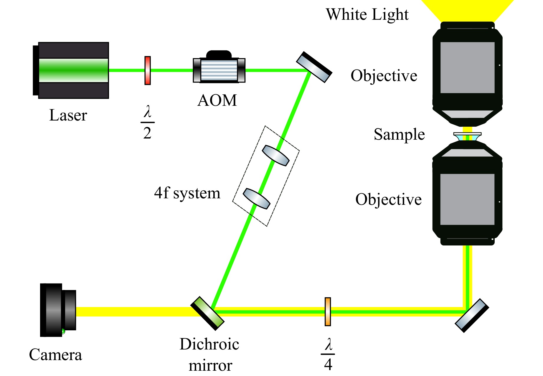
Fig. 2 Schematic of the direct laser writing (DLW) lithography optical system.
-
To pattern the sample, the piezoelectric stage was moved in the X- and Y-directions allowing for various features to be written on the PCM via a computer-driven algorithm during the lithography process. Once the desired feature was achieved on the GST thin film (Fig. 3a), a wet etch process was implemented to etch away the un-patterned (i.e. amorphous) GST leaving the crystallized GST (i.e. hard mask) virtually untouched on the surface of the sample (Fig. 3b). This step was followed by a dry etch process serving two purposes, simultaneously: etch the sample with the desired features and remove the hard mask. The following subsections describe the etching processes.
Fig. 3 a Microscope image of photothermal lithography patterned features. b Microscope image of the wet etched sample. c Scanning electron microscope (SEM) results of the SiO2 gratings achieved after the CF4 + O2 reactive-ion etching (RIE).
-
One major challenge in lithography is achieving features with favorable resolution and smooth sidewalls. Thermal lithography has an additional challenge due to the material conversion necessary in the patterning process. For example, PCM crystallization relies on the thermal absorption of the film. This requires thicker films to observe larger optical power densities which in turn jeopardizes feature linewidths. Although some PCM materials, such as Sb2Se3, show a more durable laser-induced crystallization, the grain size of crystalline Sb2Se3 is very large leading to inherent surface roughness, making it a less attractive choice for lithography40. Sb2Se3 selective wet etching also requires the use of organics-based solution (amines) which is more hazardous than tetramethylammonium hydroxide (TMAH)41. To overcome these challenges while still maintaining high-resolution patterns, GST is chosen as the PCM material for this study, and we rely on using laser pulses rather than a continuous beam for material crystallization.
Every laser pulse can be represented by a circle of radius, r, equal to half the laser spot size. The farther the pulses are, the rougher the edges of the features. Overlaying these pulses however, results in a line with stitching induced roughness, SR. By adjusting the step size (i.e. utilizing stitching features), SR can be minimized to values < 10 nm. The real limitation then becomes the feature linewidth since overlaying the pulses causes a broadening effect due to the lateral thermal dissipation discussed earlier. An in-depth summary of the stitching roughness is provided in Supplementary Information S.3 with schematics and atomic force microscopy (AFM) measurements from our study.
-
Many aqueous substances have been found to provide a selective etch between amorphous GST (aGST) and crystalline GST (cGST)42. In this work, we performed a positive-tone etch by etching the un-patterned aGST. To do so, TMAH 25 wt% solution in water was used as it has been shown to selectively etch aGST at a rate of 0.31Å/s while keeping cGST, our hard mask, virtually untouched43. This etch resulted in 100% survivability of the patterned features (Fig. 3b). The process was performed both at room temperature and under no light sensitivity limitations making this patterning process very unique.
-
The sample was then placed in a Plasmatherm Shuttleline etcher and using an optimized reactive-ion etching (RIE) recipe, a CF4 + O2 mixture was introduced to the sample which allowed the cGST hard mask as well as the exposed SiO2 substrate to be etched simultaneously and anisotropically. The etch rate was measured using companion pieces as shown in Table 1. Since the 100 nm cGST hard mask and fused silica etched in all locations at the same rate, this resulted in 110 nm deep SiO2 grating features which was also inspected using AFM measurements presented in the next section. At the end of the sample processing, near 100% yield of the patterned features is achieved.
Material Etch Rate (Å/s) cGST 6.9 SiO2 7.7 Table 1. CF4 + O2 Plasma Dry Etch Recipe Rate
-
To characterize our photothermal lithography technique, we inspected the patterned and etched sample using scanning electron microscopy (SEM), AFM, and focused ion beam (FIB). These results are summarized in the next three subsections.
-
A high resolution SEM was utilized to inspect the patterned features and etch residues, as shown in Fig. 3c. The feature size of the SiO2 grating is measured to be 387.5 nm in width, with a grating period of 975.2 nm. Additionally, we observe desirable smooth sidewalls for the SiO2 gratings after the dry etch. To further analyze the patterning quality, the gratings were characterized using AFM.
-
A Bruker AFM was used to measure feature depths as well as feature roughness on both the gratings’ surface as well as the sidewalls as demonstrated in Fig. 4. Measurements were taken after each of the following processing steps to validate expected results: DLW, TMAH wet etching, and CF4 + O2 RIE dry etching.
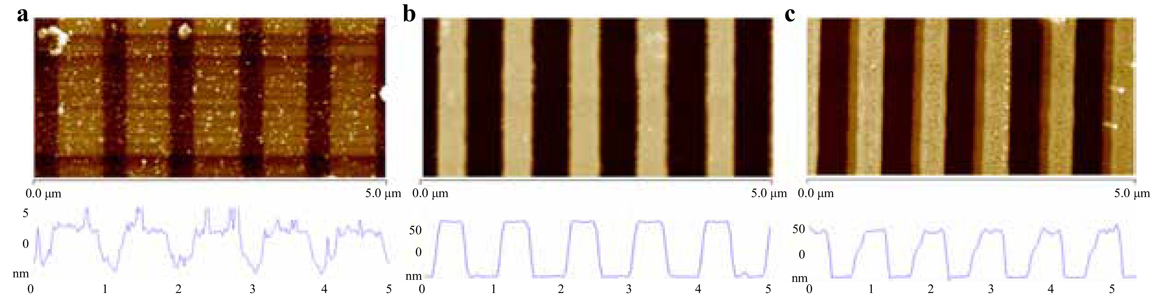
Fig. 4 AFM measurements of 100 nm GST on SiO2 showing the a ~4% compression of aGST vs. cGST gratings caused by the DLW, b TMAH wet etching of aGST, and c CF4 + O2 RIE processing resulting in the 110 nm SiO2 grating. We also present the corresponding depth measurement (in nanometers) below each figure.
After the DLW (Fig. 4a), the AFM measurements consistently showed a height reduction of ~4% between the pulsed (i.e. crystallized) area and the untouched amorphous areas. This coincides with previously demonstrated work that cGST films contract with molecule restructuring causing a thickness reduction of ~4% compared to aGST44, 45. After the TMAH wet etching (Fig. 4b), we measured a height of 100 nm confirming the complete removal of the deposited aGST film during the TMAH wet etch process. Lastly, in Fig. 4c we present the AFM measurements achieved after the complete removal of the cGST film during the RIE dry etch processing.
Additionally, Fig. 4b, c indicate that the etching process yielded grating features with smooth sidewalls. This was controlled by carefully choosing the step size between laser pulses. In depth description of the geometrical stitching process and limit is presented in section S.3 of the Supplementary Information document.
-
To determine the achievable resolution of our laser writing method, FIB milling on devices of varying stitching and thickness were conducted (Fig. 5)46. Smooth sidewalls of < 10 nm is confirmed achievable after both the wet and dry etching processes. In addition, we observe the expected undercut presented earlier as the blue region in Fig. 1b which is caused by the temperature absorption limitations in the 100 nm thick GST film.
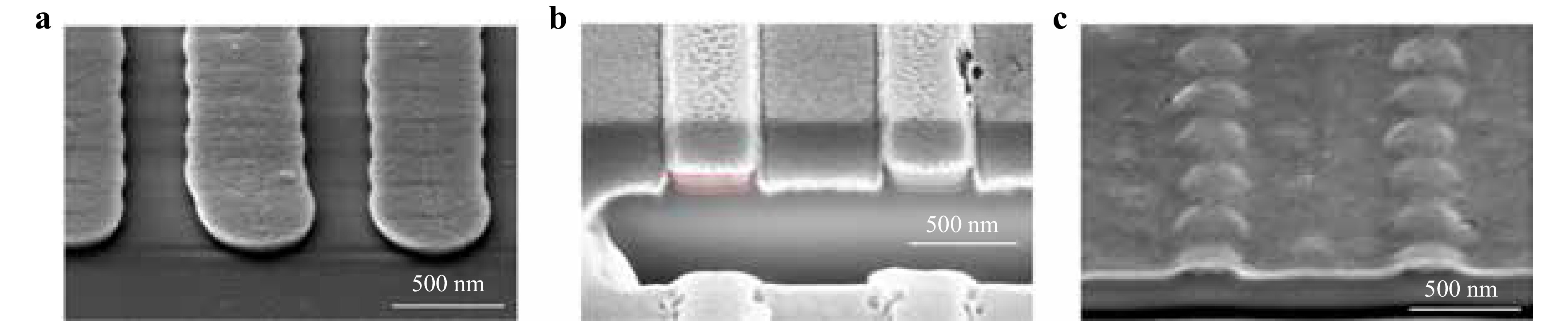
Fig. 5 FIB images of gratings patterned with a <10 nm sidewall roughness after a wet etch of 100 nm GST, b RIE etch of 100 nm GST showing the expected undercut (highlighted in red) based on the absorption modeling results, and c 50 nm thick GST film showing the expected modeled crystallization width. We illustrate the achievable resolution for features with different periodicity.
-
The above experimental results reveal our system's following advantages: (1) high resolution, (2) uniformity and reproducibility at large scale, and (3) minimized roughness via step and spot size control.
High resolution capabilities of ~300 nm linewidth has been achieved for a ~100 nm thick GST film, as verified by simulations in Fig. 1. The estimated beam size of the current system is ~270 nm, determined by the wavelength of the laser source and the numerical aperture of the optical components. Reducing aGST film thickness to ~50 nm, we show the achievable beam size to be ~200 nm for the cGST region (Fig. 5c). Additionally, the modeled undercut and linewidth of ~45 nm and ~200 nm (Fig. 1), respectively, is confirmed in Fig. 5c. Further optimization strategies, such as employing a microscope with higher numerical aperture, reducing the wavelength of light, and/or using thinner GST samples, hold promise for surpassing the diffraction limit47.
We were also able to verify that our system consistently delivers uniform and reproducible nanostructures with precise edge profiles on a large scale, demonstrated in Fig. 6a. The linewidth remains consistent under the same conditions, including laser power, film thickness, TMAH concentration, developing time, dry etch recipe, and RIE duration. To confirm the high yield and high resolution of our process, large-scale measurements are necessary, requiring a large field view at multiple features to assess both the survivability and repeatability of the patterns. Fig. 6a shows a larger range write of a 20 μm vertical grating system consisting of 21 lines, where only one major defect (caused by an accidental stage vibration) is observed. Additionally, the width of the grating lines is calculated through image analysis, showing an average of 302.6 nm grating lines and a standard deviation of only 16.1 nm across the entire sample, which is close to the surface roughness estimate.
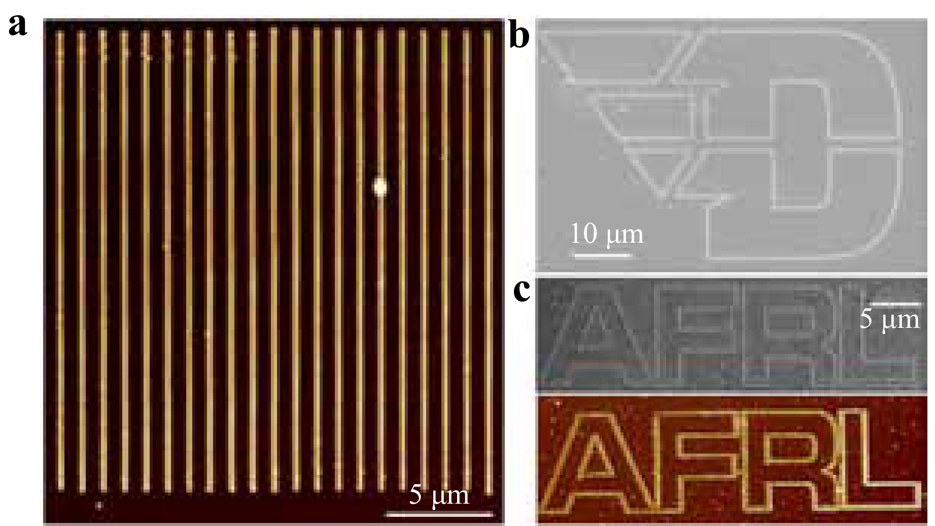
Fig. 6 a Large scale (20 μm × 20 μm) grating written with ~300 nm line width and 1 μm periodicity. b SEM image of the laser-written University of Dayton Flyers logo after TMAH wet etching. c SEM (top) of the Air Force Research Lab acronym post dry etching process and AFM (bottom) height indicating the smooth, uniform patterned features.
Lastly, the stitching induced roughness (SR) was minimized by controlling the step size and the spot size. Using this method, < 10 nm roughness has been realized during the experiments and verified by FIB milled devices presented in Fig. 5. Further roughness improvements can be implemented in the future, for example, by utilizing Sm doped GST48.
The technique also achieves satisfactory resolution for arbitrary curved patterns. In Fig. 6b, we illustrate a successfully patterned University of Dayton Flyer logo on GST thin film, subsequently etching it using the TMAH solution. The current limitation of a maximum patterning size of 80 × 80 μm2 (without stitching) primarily rises from the (X,Y) motion constraints of the piezoelectric stage in use. This versatility in arbitrary patterning opens up diverse applications, highlighting the future potential of our work (Fig. 6c). All above achievements underscore the potential of GST thin films as robust, light-insensitive heat-mode resists for high-resolution direct laser writing lithography.
-
In brief, we presented a low-cost photothermal lithography technique using photo-insensitive durable materials with a near 100% yield defined by the ratio of the number of survived features (pattern transferred on the SiO2) over the features that were initially written using the DLW system. Some of the GST samples presented in this work were processed more than a year after fabrication and exposed to varying light, temperature, and humidity conditions. Despite these factors, no change in the outcome was observed, demonstrating the long-term stability and durability of these materials. This shows a favorable alternative to current commercially available lithography tools. From design and theory to fully processed samples, we have presented the capability and high-precision of this technique. Although our feature size was limited to 80 μm × 80 μm due to the piezoelectric stage's motion, this work can easily expand to large-area features either by replacing the piezoelectric stage or through the use of stitching techniques (which is commonly used in high performance chip manufacturing processes49, 50). The reliability and uniformity of the large-area patterned features would not be jeopardized with either methodologies. Future work aimed at enhancing the resolution and versatility of this technique offers a wide range of possibilities. To improve resolution and further minimize linewidth, a laser source with a shorter wavelength, where GST exhibits higher absorption, could be utilized. Additionally, exploring different etchant chemistries may help identify a range of etching selectivities, allowing for better control over patterned depths. The versatility of the technique can also be expanded by investigating a variety of substrate materials compatible with this setup. Additionally, proper beam engineering techniques can further enable uniform periodic patterning, high-quality micrometer-scale drilling, and multi-dimensional control51−53. In brief, this technique can greatly drive lithography patterning costs down based on the optical components used in the DLW system as well as the reliable hard mask film used, hence greatly impacting the nanofabrication of various electronic, medical, and military devices.
-
We acknowledge collaboration and funding from Air Force Research Laboratory (FA9550-23RYCOR001).
Direct laser writing lithography of photo-insensitive durable GST thin films with near 100% yield
- Light: Advanced Manufacturing , Article number: (2025)
- Received: 23 December 2024
- Revised: 20 August 2025
- Accepted: 06 September 2025 Published online: 27 October 2025
doi: https://doi.org/10.37188/lam.2025.075
Abstract: Modern technologies have been heavily reliant on semiconductor chips driving their innovation. These nanoscale-featured devices have created the need for precise lithographic tools that enable the microscopic patterning of such features. With a large drive to keep the cost of lithography tools low while maintaining high resolution, recent works have explored alternate solutions to existing commercial tools. Therefore, this study investigates a low-cost photothermal lithography technique that utilizes a phase-change material to allow for high-resolution 200 nm features to be patterned. The technique we present in this work does not only provide a sidewall roughness of < 10 nm but also uses light-insensitive materials, allowing for delicate features to be patterned under non-restrictive environments. We present the theoretical limits of our laser writing system and demonstrate the experimentally achieved features, describing in detail how we overcome some of the diffraction and thermal limits in order to achieve ultimate resolution and sidewall roughness. This was achieved with near 100% yield as every patterned feature survived all stages of the sample processing with minimal defects.
Research Summary
Photothermal Lithography: High-Resolution, Low Roughness
This study explores a low-cost photothermal lithography technique using light-insensitive Ge2Sb2Te5 phase-change material to achieve 200 nm features with sidewall roughness under 10 nm. We demonstrate the system’s theoretical and experimental capabilities, achieving near 100% yield with reduced lithography costs while maintaining high resolution. Samples showed no degradation even after a year under varying environmental conditions, proving the durability of the materials used. Although pattern size was limited to 80 μm × 80 μm due to stage motion, this can be scaled using larger stages or stitching. Using shorter-wavelength lasers to enhance resolution, new etchant chemistries for depth control, and beam engineering for uniform patterning would allow this versatile, cost-effective technique to have significant potential in fabricating electronic, biomedical, and defense devices.
Rights and permissions
Open Access This article is licensed under a Creative Commons Attribution 4.0 International License, which permits use, sharing, adaptation, distribution and reproduction in any medium or format, as long as you give appropriate credit to the original author(s) and the source, provide a link to the Creative Commons license, and indicate if changes were made. The images or other third party material in this article are included in the article′s Creative Commons license, unless indicated otherwise in a credit line to the material. If material is not included in the article′s Creative Commons license and your intended use is not permitted by statutory regulation or exceeds the permitted use, you will need to obtain permission directly from the copyright holder. To view a copy of this license, visit http://creativecommons.org/licenses/by/4.0/.

 DownLoad: