


-
Photothermal conversion materials are a class of materials that transform absorbed radiation photons into thermal energy via non-radiative transitions, such as photon-phonon interactions and vibrational relaxation1, typically including metal nanoparticles2 and carbon-based materials, such as carbon nanotubes3 and carbon dots4. Thermoelectric conversion is a physical process that directly converts thermal energy into electrical energy, fundamentally based on the Seebeck effect5. When two different conductive or semiconductive materials form a closed circuit with a temperature difference at their junctions, charge carriers at the hot side tend to diffuse toward the cold side. Due to the differing responses of charge carriers in distinct materials, a potential difference is established at the junctions, generating an electric current. Common thermoelectric materials include GaAs, PbTe, and various carbon-based materials6. Among these, carbon nanotubes (CNTs), possessing broadband light absorption ranging from millimeter waves to visible light and solution processability, emerge as promising candidates for photo-thermoelectric (PTE) conversion applications7–9.
Quality control prior to pharmaceutical market distribution is of paramount importance10. On one hand, this necessitates non-destructive testing that relies on the transmissivity of the material to the probing light source; ultra-broadband, multi-wavelength optical measurements in the sub-terahertz to infrared range enable non-destructive identification of non-metallic materials such as polymers, glass, semiconductors, ceramics, and liquids11. On the other hand, in-line real-time monitoring imposes stringent requirements on the miniaturization of the equipment. Therefore, non-destructive testing techniques should be performed on-site without disturbing the original environmental conditions of the target, such as its scale or flow rate. CNT thin-film arrays12 can be fabricated with CNTs are into using techniques such as inkjet printing13, self-aligned filtration14, or laser ablation. A p-n junction is formed within the p-type CNT film by casting a chemically n-type doping solution, typically a mixture of hydroxide and crown ether aqueous solutions15, which serves as the photoelectric detection interface. Based on the Seebeck effect, external illumination of the p-n junction photoelectric interface generates a PTE response. By optimizing doping concentration, material properties, and dimensional design, and by integrating appropriate detection light sources, miniaturization and integration of the detection device can be achieved.
In a recent study published in Light: Science & Applications, Li et al16. from the Department of Electrical, Electronic, and Communication Engineering, Faculty of Science and Engineering, Chuo University, demonstrated a CNT thin-film array-based PTE imager fabricated via inkjet printing capable of photodetection across multiple light sources and broad spectral bands (Fig. 1). Utilizing the CNT film PTE imager within a transmission optical system under external broadband sub-terahertz to infrared (4.33−909 μm wavelength range) irradiation, non-destructive in-line dynamic pharmaceutical monitoring was achieved at a maximum scanning speed of 3 mm·s−1. Furthermore, combined with a hybrid system incorporating reflective scanning, the approach provided detailed surface state information of metallic impurities concealed within pharmaceutical pills. In future work, by optimizing the readout circuitry of the carbon nanotube thin-film PTE imager, the theoretically estimated operating speed could reach 270 mm·s−1, which is expected to promote its practical application in real-world scenarios (> 200 mm·s−1).
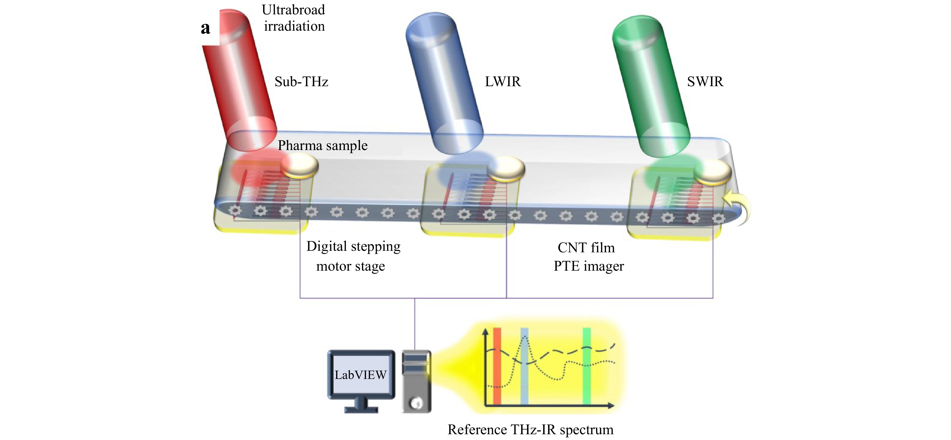
Fig. 1 Conceptual diagram of the CNT thin film PTE imager. Images reproduced from Ref. 16 under the terms of the Creative Commons CC BY license.
Currently, CNT thin-film PTE imager devices possess significant advantages in miniaturization and integration. The next major objective is to enhance the pixel density of detection and improve the resolution of image acquisition. Achieving this requires more densely packed CNT arrays fabricated by advanced printing technique, as well as optimized interface circuitry. Additionally, due to insufficient diffusion of the n-type liquid dopant into the original p-type film channels, traditional printing methods for CNT PTE sensors suffer from low efficiency in manufacturing each pixel. To address the optimization of p-n junction fabrication, Li et al.17 proposed a high-yield method for producing p-n junction PTE sensors using p-type and n-type CNT inks, which provides a potential solution. Furthermore, increasing the material’s absorption rate, photothermal conversion efficiency, and thermoelectric conversion efficiency will further improve the sensitivity of the PTE imager. The progressive resolution of these challenges is expected to advance the commercialization of CNT film PTE imagers, providing excellent solutions for portable, in situ, and real-time monitoring applications. In addition, photothermal/thermoelectric/photothermal-electric conversion materials have also shined in many other areas, such as tumor treatment18–20, seawater evaporation21, and clean energy conversion22.
HTML
-
This work was supported by the Science and Technology Development Fund of Macau SAR (0139/2022/A3, 0002/2024/TFP).

 DownLoad: