


-
The robust and stable joining of dissimilar materials, such as metals and transparent materials (e.g., glasses and crystals) plays a vital role in the development of advanced optical, electronic, and energy systems1,2. In applications, such as high-power laser systems, aerospace sensors, and precision medical devices, integrating functional glass components with metallic structures is essential for achieving compact, reliable, and high-performance assemblies3,4. However, the fundamental mismatch between the optical, thermal, and mechanical properties of these materials presents significant challenges in achieving strong, hermetic, and long-lasting joints5,6. Traditional bonding methods, such as adhesives or thermal joining, often exhibit limitations in mechanical strength, thermal resilience, and environmental compatibility7. These challenges are increasingly significant in sustainable manufacturing and green engineering, where clean, precise, and scalable joining technologies are urgently required to minimize material waste, energy consumption, and operational failure risks. Thus, developing advanced joining strategies that ensure structural integrity without compromising functionality is critical for supporting the emerging demands in chemical engineering, photonic integration, and energy-efficient system design8,9.
Recent advances in ultrafast laser technologies have enabled the of joining dissimilar materials through noncontact, localised energy deposition with submicrometric precision10,11. Among these, ultrafast laser welding has emerged as a promising solution for transparent-to-metal bonding because of its ability to induce nonlinear absorption in transparent media and generate confined melting with minimal thermal damage. This process eliminates the need for intermediate layers or adhesives and offers a clean and scalable route for hybrid material integration12,13. Importantly, the precision and flexibility of ultrafast laser processing make it particularly suitable for fabricating miniaturised devices and complex microstructures in fields, such as microoptics, photonics, and sustainable electronics14,15.
Despite significant progress in ultrafast laser joining techniques, most existing studies on metal-glass welding rely on highly polished metallic surfaces to achieve optical contact, a condition where the interfacial gap is less than approximately one-quarter of the shortest visible wavelength, thereby ensuring intimate physical contact and uniform laser energy absorption across the interface16,17. These idealised conditions minimise optical scattering and improve the quality of the resulting joint. However, such polished surfaces are rarely encountered in practical applications, where components often exhibit inherent or process-induced roughness owing to machining, wear, or design constraints. In particular, when the surface roughness (Sa) exceeds 1 μm, challenges in achieving effective interfacial coupling become substantially more pronounced18,19. The roughness introduces several complications: first, it results in poor physical contact between the glass and metal, creating gaps that hinder localized melting and bond formation20. Second, the nonuniform surface topography causes inconsistent absorption and scattering of the laser beam, reducing the process stability and increasing the likelihood of defects, such as pores, cracks, or voids21. Third, high-roughness interfaces tend to disrupt capillary-driven melt flows and solidification dynamics, making it difficult to form strong and continuous joints22. Consequently, achieving the robust and reproducible welding of rough metals to transparent materials remains a formidable technical barrier. Addressing this challenge is essential for enabling the scalable and sustainable integration of optical, electronic, and structural functionalities in advanced manufacturing platforms.
Despite recent advances in the ultrafast laser joining of dissimilar materials, the underlying mechanism of non-optical-contact welding between transparent and metal materials remains poorly understood1,18,23. In such configurations, a relatively large air gap exists at the heterogeneous interface, severely impeding effective energy coupling and resulting in unavoidable ablation on both the metal surface and rear side of the transparent material under ultrafast laser irradiation24,25. From this perspective, understanding the integration between ultrafast laser and heterogeneous interfaces, as well as developing effective strategies to fill the interfacial air layer, is essential for advancing the welding mechanism under non-optical-contact conditions. Early studies on femtosecond laser welding of rough copper and glass indicated that metal nanoparticles generated by ablation might serve as interfacial fillers; however, the resulting joint strength was limited to approximately 1 MPa26. More recent research has demonstrated that millijoule-level femtosecond pulses can simultaneously induce plasma generation in glass, air, and metals at the interface. The resultant multiphase plasma mixing and hybrid melting of glass and metal enable enhanced bonding, achieving shear strengths of up to 8.94 MPa19,27. In addition, the heat accumulation effects induced by high-repetition-rate ultrafast lasers (typically exceeding 200 kHz) have been widely applied in dissimilar material welding28–30. For instance, repeated irradiation at 400 kHz facilitates controlled melting and interfacial flow between the metal and transparent substrates, effectively filling the interfacial gap without the need for optical contact25,31. Despite recent progress, a unified understanding of the welding mechanism for non-optical contact transparent/metal dissimilar materials has yet to be established, representing a critical and unresolved challenge in the field. More importantly, the unclear understanding of the underlying mechanisms makes it difficult to identify the dominant factors limiting joint performance and hinders the development of effective and targeted research strategies.
With recent advancements in various in situ monitoring and analysis techniques32–34, combined with the widespread application of spatial-temporal shaping of ultrafast laser35–38, new opportunities have emerged to investigate the welding mechanisms of non-optical-contact transparent/metal dissimilar materials. Regarding in situ monitoring and analysis techniques, within the femtosecond-picosecond-nanosecond timescales, pump-probe detection methods enable the comprehensive analysis of plasma generation, laser energy absorption, and material phase transitions39. On the microsecond timescale, continuous high-speed imaging can capture the transient nonlinear absorption processes inside transparent materials and reveal the free expansion of plasma during the ultrafast laser welding of transparent materials40. Meanwhile, in terms of spatial-temporal shaping, typical approaches, such as Bessel beams and Burst modes, have been validated to effectively enhance the welding performance of transparent materials. In this regard, Burst-mode femtosecond laser processing has attracted increasing attention41,42. By temporally structuring multiple sub-pulses within a single Burst envelope, this technique enables cumulative energy deposition, offering enhanced control over plasma dynamics and heat diffusion processes43,44. These characteristics provide distinct advantages for modulating interactions at complex or imperfect interfaces and position Burst-mode welding as a promising strategy for addressing performance limitations in practical dissimilar material systems. However, studies applying these approaches to non-optical contact transparent/metal dissimilar material welding remain extremely limited.
However, in the context of the non-optical-contact welding of transparent/metal heterogeneous materials, key questions remain unresolved, including how linear absorption in metals couples with nonlinear absorption in transparent materials and how materials across a non-optical-contact heterogeneous interface mix. To our knowledge, no relevant studies or reports are currently available, and these critical aspects remain major unresolved challenges in the field. In this context, we explored the ultrafast laser welding of sapphire and Invar alloy, a representative transparent-metal heterojunction, under Burst-mode femtosecond irradiation. Invar substrates with an average surface roughness exceeding 2 μm were used to reflect the manufacturing-relevant surface conditions. Despite expectations that the Burst configuration would play a critical role in determining the joint quality, the resulting weld strengths remained consistently in the range of 9–13 MPa across the different burst settings. This unexpected outcome prompted a detailed investigation of weld morphology, cross-sectional microstructure, and interfacial elemental profiles. The insights gained offer a deeper understanding of Burst-mode welding mechanisms and support the development of robust, low-preparation joining strategies for dissimilar materials in high-performance and sustainable manufacturing applications.
-
Under the focusing of an 80 mm focal length telecentric lens, Burst-mode femtosecond laser welding was performed at the interface between rough Invar alloy (Fe-36Ni) and sapphire using a focal spot size of 33 μm and scanning speed of 40 mm/s. The femtosecond laser featured a Rayleigh length of up to 300 μm, effectively accommodating the surface irregularities of the rough metal. This welding configuration, with a large processable area of 40 × 40 mm2 and high scanning speed, is suitable for heterogeneous material integration in diverse application scenarios (Fig. 1a). In the experiments, the Invar alloy had a surface roughness of Sa = 2.128 μm, with some surface scratches reaching depths of 2 μm. The sapphire surface exhibited a roughness of Sa = 1.464 μm. (Fig. S1 in Supplementary S1, Supporting Information). To the best of our knowledge, this is the roughest non-optical-contact metal/transparent dissimilar material reported to date for ultrafast laser welding1. To facilitate effective thermal accumulation, a 200 kHz Burst-mode femtosecond laser was employed. The non-Burst (single-pulse) configuration and various Burst configurations shared an identical total pulse energy of 132.5 μJ. The number of sub-pulses per Burst can be tuned from 1 to 12.
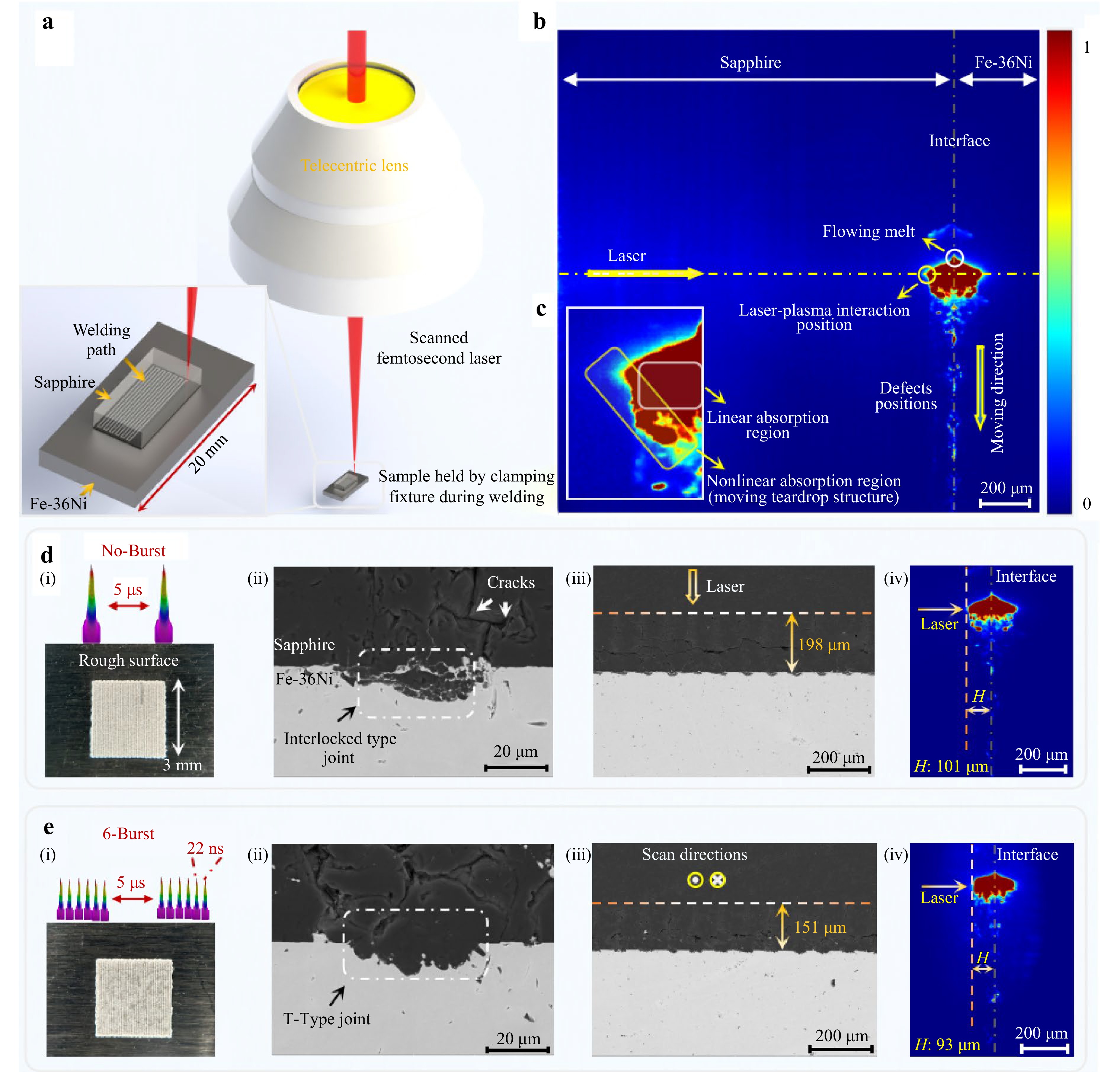
Fig. 1 Burst-mode femtosecond welding method, process, and results. a Galvanometer-based welding system, weld samples, and welding path. b High-speed imaging result of the ultrafast laser welding process, showing the transient laser absorption process. c Linear and nonlinear absorption regions during the femtosecond laser welding process. d Non-Burst mode ultrafast laser welding results and its transient absorption process (acquired at 100 ms). e 6-Burst mode ultrafast laser welding results and its transient absorption process (acquired at 100 ms). In d and e, (i) represents the upper surface of the welds, (ii) the cross-sectional profiles of the welds, (iii) the cross-sectional profiles of the modified structure within the sapphire, and (iv) the plasma morphology.
Furthermore, high-speed imaging was employed to continuously monitor and analyse the transient process of femtosecond laser welding at the transparent/metal heterogeneous interface (Figs. S2 and S3 in Supplementary S2, Supporting Information). Fig. 1b presents a representative frame captured under stable welding conditions, marking the first dynamic visualisation of femtosecond laser welding between transparent and dissimilar metals. By capturing the spatial distribution and intensity of the plasma generated during welding, the transient energy deposition at the sapphire-metal interface was revealed, and several intriguing phenomena were observed throughout the dynamic imaging sequence. For example, when the interface was irradiated by a femtosecond laser, plasma was generated at the focal centre. However, owing to the movement of the sample, a notable melt flow was observed away from the irradiated region (marked in Fig. 1b). Considering that no significant plasma distribution due to free expansion at the interface was detected in the nonwelded region, it is inferred that the plasma was effectively confined at the interface39,45. This confinement implied that the molten metal was actively driven to fill the interfacial gap, thereby facilitating the transition from non-optical-contact to optical-contact welding. Moreover, at the focal position of the femtosecond laser, the maximum vertical extension of plasma within the sapphire reached approximately 106 μm (Fig. 1b). During sample translation, a droplet-shaped molten zone formed inside the sapphire and exhibited a tilted spatial distribution, resembling the teardrop structures previously reported in the femtosecond laser welding of transparent materials46. However, for transparent/metal dissimilar material welding, both nonlinear absorption in the transparent material and linear absorption in the metal contribute to the overall laser energy deposition. Consequently, the plasma formation region reflects the combined absorption process at the interface, as shown in Fig. 1c. Notably, even nearly 1 mm away from the laser irradiation centre, several bright regions were still visible at the interface, indicating the formation of defects, such as stress-induced microcracks.
Fig. 1d, e present the surface morphologies and cross-sectional profiles of Invar-sapphire welds fabricated under non-Burst and 6-Burst femtosecond laser welding modes, respectively. After welding under the non-Burst mode, the sample surface exhibited uniform white strip-like textures, primarily attributed to microcracks in the sapphire. These linear textures were aligned with a predefined scanning trajectory and oriented perpendicular to the scratch marks on the rough Invar surface (Fig. 1d(i)). In contrast, under the 6-Burst mode, the texture inside the transparent material appeared less uniform, with intermittent dark spots distributed along the weld track (Fig. 1e(i)). These darker features expanded progressively with increasing numbers of sub-pulses, indicating that Burst-mode processing effectively suppressed microcrack formation in the Invar-sapphire welds. In the cross-sectional profiles of the Invar sapphire welds, the sapphire was embedded into the Invar alloy (Fig. 1d(ii), e(ii)). During the femtosecond laser heating of a heterogeneous interface, a portion of the laser energy is deposited through nonlinear absorption within the transparent material47, whereas the remaining transmitted energy simultaneously interacts with the metal surface. Consequently, both the sapphire and Invar underwent localised melting. In both welding modes, the sapphire penetrated the Invar alloy, indicating that molten Invar was displaced into adjacent free spaces by the expanding molten sapphire. The absence of visible air gaps in the weld cross-sections further confirmed this effect. In addition, the protruding region observed in the plasma image likely corresponded to the molten metal (Fig. 1b).
However, clear differences are observed in the cross-sectional profiles of the welds between the two modes. Under the non-Burst mode, the expansion of molten sapphire into the metal formed an interlocking structure with partially melted Invar (Fig. 1d(ii)). In contrast, the 6-Burst mode produced a distinct layered interface between sapphire and Invar, forming a “T”-shaped weld (Fig. 1e(ii)). The non-Burst mode delivered pulses with six times the energy of each sub-pulse under the 6-Burst mode, resulting in a higher peak power density and stronger recoil forces. This resulted in the rapid flow of the molten metal toward the centre and the formation of interlocks.
The modified sapphire structure was also analysed. Under the non-Burst mode, the modified zone extended to a height of 198 μm (Fig. 1d(iii)), whereas under the 6-Burst mode, it reached 151 μm (Fig. 1e(iii)). Although Burst-mode femtosecond lasers are generally capable of inducing larger modified volumes within transparent materials48, the observed reduction in teardrop height under 6-Burst conditions suggests that the energy delivered by each sub-pulse was below the sapphire modification threshold. During 6-Burst welding, the lower peak power density of each sub-pulse limited the plasma growth in regions farther from the interface, resulting in a smaller modified region. From the plasma morphology obtained after welding reached steady state under both modes, the plasma height was 101 μm under the non-Burst mode and 93 μm under the 6-Burst mode (Fig. 1d(iv), e(iv)). Although the central plasma width remains nearly constant, the apex width increases significantly under the 6-Burst mode, nearly matching the central width. This broader apex indicates that the 6-Burst mode, through enhanced thermal accumulation, sustained plasma activity at the upper boundary through enhanced thermal accumulation and facilitated the formation of a wider modified region within the transparent material (Figs. S4 and S5 in Supplementary S3, Supporting Information).
The cross-sectional morphologies of the welds and modified regions inside the sapphire under different sub-pulse numbers are shown in Fig. S6 (Supplementary S3, Supporting Information). Under the 2-Burst welding mode, the Invar-sapphire heterogeneous interface continued to exhibit an interlocking structure. However, only localised regions showed the molten metal flowing into the molten sapphire. Simultaneously, the modified region within the sapphire decreased in height to 171 μm. As the number of sub-pulses increased to 6, all heterogeneous interface transitioned into a “T”-shaped configuration. Moreover, with increasing sub-pulse numbers, the interaction width between the heterogeneous interface decreased from approximately 40 μm to around 20 μm, while the embedded depth of sapphire increased to approximately 10 μm. Furthermore, regarding the height of the laser-modified region within sapphire under different Burst modes, the modification depth stabilised at approximately 151 μm when the number of sub-pulses increased to four, with minimal variation (Fig. S7 in Supplementary S2, Supporting Information). This result indicates that under higher sub-pulse numbers, the laser energy deposition depth in sapphire was predominantly governed by the linear absorption of the Invar alloy rather than by nonlinear interactions in the transparent material.
-
In non-optical-contact transparent metal dissimilar-material welding, a fundamental question that remains unresolved is how ultrafast laser energy is deposited at a heterogeneous interface. Specifically, how does linear absorption in a metal couple with nonlinear absorption in a transparent material under ultrafast laser irradiation, and how do these mechanisms facilitate the heating, melting, and welding of the heterogeneous interface? Although several descriptive interpretations have been proposed, such as metal-dominated linear absorption inducing subsequent heating and melting of the transparent material49 or filling of the interface by ablation-induced nanoparticles26,50, direct experimental evidence to analyse and validate these mechanisms is lacking. To address this knowledge gap, we employed an established high-speed plasma imaging system to systematically investigate the laser energy deposition process in non-optical-contact transparent-metal dissimilar materials. Additionally, we examined the influence of different Burst-mode femtosecond laser welding techniques on complex energy coupling and deposition behaviour.
A frame rate of 9000 fps was selected during high-speed plasma imaging, and the repetition rate of the ultrafast laser was 200 kHz. This indicates that approximately 22 fs pulses interacted with the target within each imaging cycle. Under the non-Burst mode, the pulse energy was 132.5 μJ, whereas under the 6-Burst mode, each sub-pulse carried an energy of 22.1 μJ. Fig. 2a presents the first nine frames of plasma evolution. Under the non-Burst mode, the femtosecond pulse energy exceeds the sapphire modification threshold. From the third frame onwards, a continuous energy deposition region-reaching a length of nearly 800 μm was observed inside the sapphire. As the irradiation duration increased, this energy-deposited region gradually shifted toward the top surface of the sapphire. Considering the relative movement of the sample with respect to the laser during continuous irradiation, this shift indicated that the plasma, initially triggered by nonlinear absorption within the sapphire, propagated and was sustained along the laser incident direction31. Under the non-Burst femtosecond laser welding of the sapphire-Invar heterogeneous interface, high-energy femtosecond pulses were observed to excite the plasma within the sapphire, while a portion of the laser energy was also deposited at the sapphire-Invar interface. This interfacial energy deposition is primarily governed by the linear absorption of the Invar alloy51. However, with prolonged irradiation, the total femtosecond laser energy deposited at the sapphire-Invar interface decreased significantly owing to prior energy absorption within the sapphire, resulting in only minor variations in the plasma volume at the interface39. In contrast, under the 6-Burst mode, owing to the significantly reduced single-pulse energy of the femtosecond laser, nonlinear absorption was no longer induced within the sapphire; thus, no internal modification region was formed. Under Burst-mode conditions, for the same irradiation duration, the amount of femtosecond laser energy deposited at the sapphire–Invar heterogeneous interface was significantly higher than that under the non-Burst mode. Consequently, the plasma volume generated under the 6-Burst mode exhibited a significant increase within the same irradiation time.
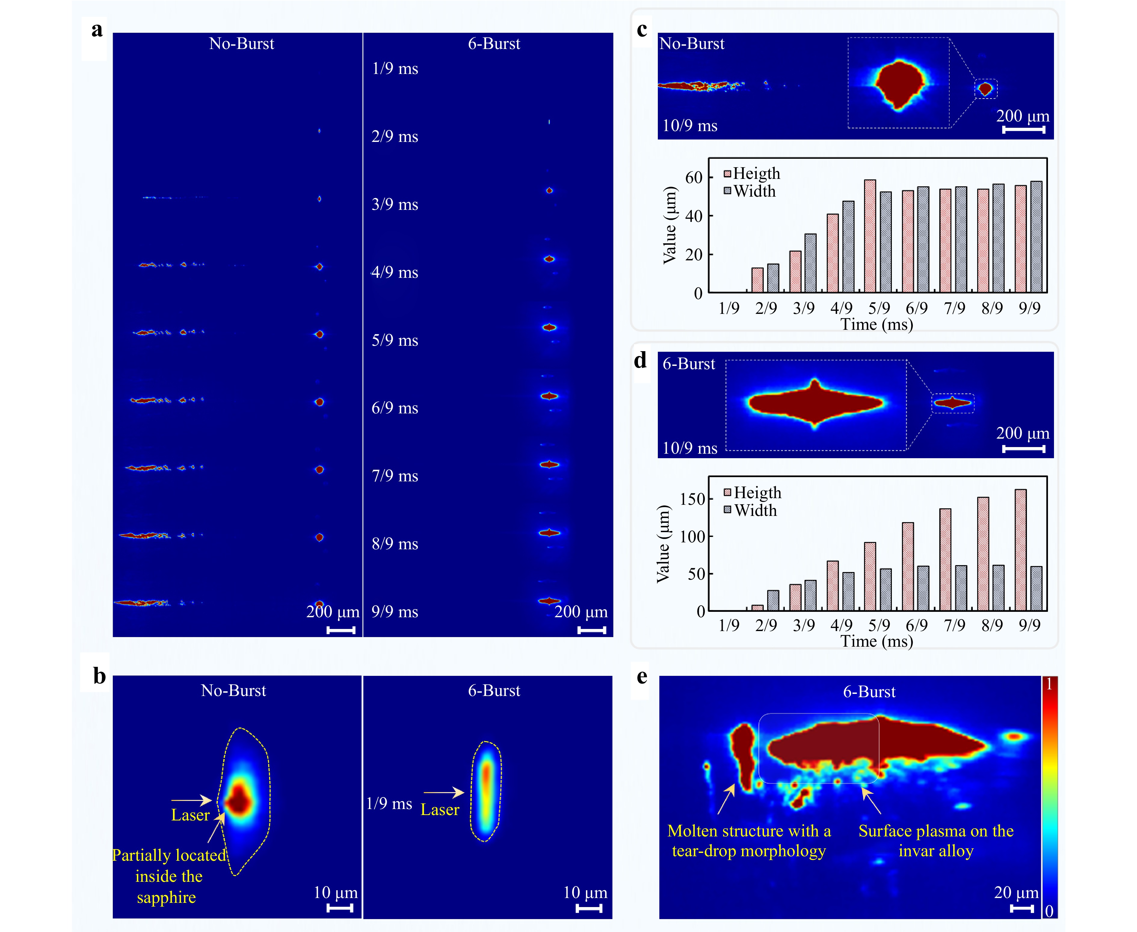
Fig. 2 Femtosecond laser energy transient deposition processes in different Burst modes. a Comparative analysis of laser energy deposition over a 1 ms interaction duration. b Comparison of initial plasma morphologies at heterogeneous interfaces. Plasma evolution and size variation characteristics under c non-Burst, and d 6-Burst femtosecond laser irradiation. e Plasma morphology at 150/9 ms under the 6-Burst mode. The image reveals a continuously growing tear-shaped structure within the sapphire due to nonlinear absorption, and a surface plasma on the Invar alloy dominated by linear absorption.
Conversely, we further examined the first-frame plasma images under both modes. With a spatial resolution as high as 2 μm, the plasma imaging offered a robust support for analysing the energy deposition process (Fig. 2b). Considering the presence of a 4–5 μm air gap between the sapphire and Invar under the welding conditions, we offered an intriguing new insight into the femtosecond laser welding mechanism for non-optical-contact transparent/metal dissimilar materials. First, in Fig. 2b, we highlight the diffusion range of the plasma, which freely expands within the air layer of the heterogeneous interface. Under the non-Burst mode, the centre of the captured plasma image appeared deep red, indicating a plasma density close to the highest level detected by high-speed imaging. Considering the short irradiation duration, it can be inferred that the femtosecond laser pulse energy was sufficient to excite the metallic plasma on the Invar surface. Moreover, at the centre of the laser interaction, the plasma had already begun to expand opposite to the direction of laser incidence, and a high-density plasma region was formed within the sapphire. From this perspective, at the initial stage of sapphire–Invar welding, the femtosecond laser energy initially excited a dense, high-temperature plasma on the Invar surface. This metallic plasma simultaneously expanded along the free space of the heterogeneous interface and grew backward along the laser incidence direction, thereby triggering plasma formation within the sapphire substrate25. At this moment, the metallic and sapphire plasmas can be considered to have fully interacted and mixed19. Note that this description corresponds to the energy deposition process under the non-Burst mode, where the pulse energy is sufficiently high. Even though part of the energy was absorbed within the sapphire, a considerable portion of the femtosecond pulse energy still reached the sapphire–Invar heterogeneous interface9,39.
In contrast, under the 6-Burst mode, the energy of a single femtosecond pulse was significantly reduced. Under these conditions, the femtosecond laser initially ablated the Invar surface at the heterogeneous interface, thereby exciting the plasma. The plasma density excited under the 6-Burst mode was notably lower than that under the non-Burst mode. Moreover, owing to the relatively low energy of each sub-pulse, the distance over which the plasma diffused within the air layer at the heterogeneous interface was reduced. However, the application of six sub-pulses on the Invar surface under the 6-Burst mode resulted in higher thermal accumulation and consequently enhanced laser energy deposition. Therefore, the high-density plasma region along the interface extended to 37 μm, compared to 23 μm in the non-Burst mode (Fig. 2b). Additionally, during the downward high-speed movement of the sample, the femtosecond laser was incident on Invar at a relatively high angle. In this configuration, the generated plasma is compressed against the space occupied by the upper plasma. Therefore, in the plasma distribution captured in Fig. 2b under the 6-Burst mode, the intensity in the upper half of the image was higher.
After elucidating the initial process of femtosecond laser energy deposition at the sapphire–Invar heterogeneous interface, a key question arises regarding the onset of sapphire melting at this interface. Considering that Invar is an opaque material, it is challenging to directly analyse its heating and melting behaviours using plasma imaging. To investigate this, we focused on the tenth frame of the plasma imaging sequence, corresponding to 1.1 ms, and compared the captured images obtained under the two irradiation conditions (Fig. 2c, d, and Fig. S8 in Supplementary S4, Supporting Information). At this moment, the volume of the laser-modified region within the transparent material increased further under both conditions. Owing to the relative motion of the sample, the bottom portion of the deep red plasma region in the image corresponds to the previously modified zone at the interface, confirming that localised melting occurred within the sapphire. In addition, under the non-Burst condition, partial melting was observed near the top surface of the sapphire. These observations confirmed that during femtosecond laser welding of the sapphire–Invar heterogeneous interface, the melting of the transparent material occurred on a millisecond timescale.
In addition, the free plasma expansion observed in Fig. 2b is no longer present in the plasma images shown in Fig. 2c, d. Under the Burst mode irradiation, pronounced molten material flow and protrusion at the interface were observed. These plasma imaging results strongly support the occurrence of active molten material flow and filling during femtosecond laser welding. The metallic material melted and flowed into the air gap at the sapphire–Invar heterogeneous interface, spontaneously filling the space and transforming the non-optical-contact interface into an optical-contact interface. Free expansion of the generated plasma was effectively suppressed as the original free space became a confined volume. In this regard, we recall the plasma imaging results obtained during single-point femtosecond laser irradiation at the sapphire–stainless steel heterogeneous interface. Free plasma expansion was observed under single-point (nonscanning) irradiation. However, under actual scanning-based welding conditions, this study reveals, for the first time, the heating, melting, and spontaneous filling of the molten material at the interface, offering a new mechanistic understanding of femtosecond laser welding of nonoptical-contact transparent/metal heterogeneous materials39.
Based on the preceding analysis, a comparison of the spatial dimensions of the laser-deposited regions under the two welding modes (Fig. 2c, d) revealed that under the non-Burst mode, the femtosecond laser induced nonlinear absorption within the sapphire, limiting the energy ultimately deposited at the interface. Consequently, the plasma volume significantly increased within the first 0.55 ms, after which both the width and height stabilised at approximately 55 μm. In contrast, under the Burst mode, the overall deposited energy was enhanced, whereas the peak power density of each sub-pulse was reduced. Consequently, the plasma height continuously increased up to 1.00 ms, reaching a maximum of 160 μm, whereas the width remained stable at approximately 50 μm after 0.55 ms. This comparison indicated that, under the Burst mode, the energy deposited within the transparent material at the interface was significantly enhanced, and the growth of plasma within sapphire, opposing the laser incident direction, proceeded at a faster rate52.
Finally, the plasma images at frame 150 and its surrounding frames were analysed to further illustrate the coupling between the linear absorption in Invar and nonlinear absorption in sapphire during femtosecond laser irradiation (Fig. 2e and S9 in Supplementary S4, Supporting Information). Based on the preceding analysis, the temporal sequence of femtosecond laser energy deposition at the sapphire-Invar heterogeneous interface was identified. With increased irradiation time, the plasma generated at the interface was sustained, resulting from both the linear absorption of the femtosecond laser by the Invar surface and subsequent nonlinear absorption within the sapphire. These coupled absorption processes jointly maintain the surface plasma at the heterogeneous interface (as shown in Fig. 2e). Interestingly, plasma imaging also revealed the presence of an upward-growing plasma region above the interface, whose morphology resembled the teardrop-shaped molten structures formed in ultrafast lasers of transparent materials53. Dynamic analysis of this feature confirmed that (Fig. S9 in Supplementary S4, Supporting Information), during the sapphire–Invar welding process, isolated modified regions also formed within the transparent material. In contrast to those formed under the non-Burst mode, these regions originated from sustained plasma growth initiated by linear absorption at the Invar surface.
In summary, this section presents a direct visualisation and an in-depth mechanistic understanding of ultrafast laser energy deposition at non-optical-contact interfaces between transparent and metallic materials. Using high-speed plasma imaging with high spatial and temporal resolutions, this study revealed the sequential and coupled absorption processes, initiated by linear absorption at the metal surface, followed by nonlinear absorption within the transparent material, which jointly sustains plasma generation at the heterogeneous interface. Importantly, this study demonstrates, for the first time, spontaneous molten material flow and interfacial filling under scanning-based femtosecond laser irradiation, offering compelling experimental evidence for the transition from a non-optical contact to an optical-contact interface. These findings establish a new mechanistic framework for understanding energy coupling and material interactions in the ultrafast laser welding of dissimilar material systems.
-
Fig. 3 and S10 (Supplementary S5, Supporting Information) show the cross-sectional morphologies of the sapphire-Invar welds under different femtosecond laser modes. In all cases, the sapphire was embedded into the Invar material at the interface. Considering the large difference in thermal expansion coefficients between the two materials, 5.0 × 10⁻⁶/K for sapphire and 1.2 × 10⁻⁶/K for Invar, the molten sapphire underwent a larger free expansion. In conjunction with the absorption behaviour (linear absorption in Invar and nonlinear absorption in sapphire), and the final weld morphology, the melting depth of Invar did not exceed 20 μm, significantly smaller than the modification depth in sapphire (exceeding 150 μm). This indicates that both the modified volume and height within the sapphire significantly exceeded those in the metal, resulting in a higher degree of reversible expansion. Consequently, the molten sapphire compresses the underlying molten Invar, forming a morphology in which the sapphire is embedded in the Invar substrate.
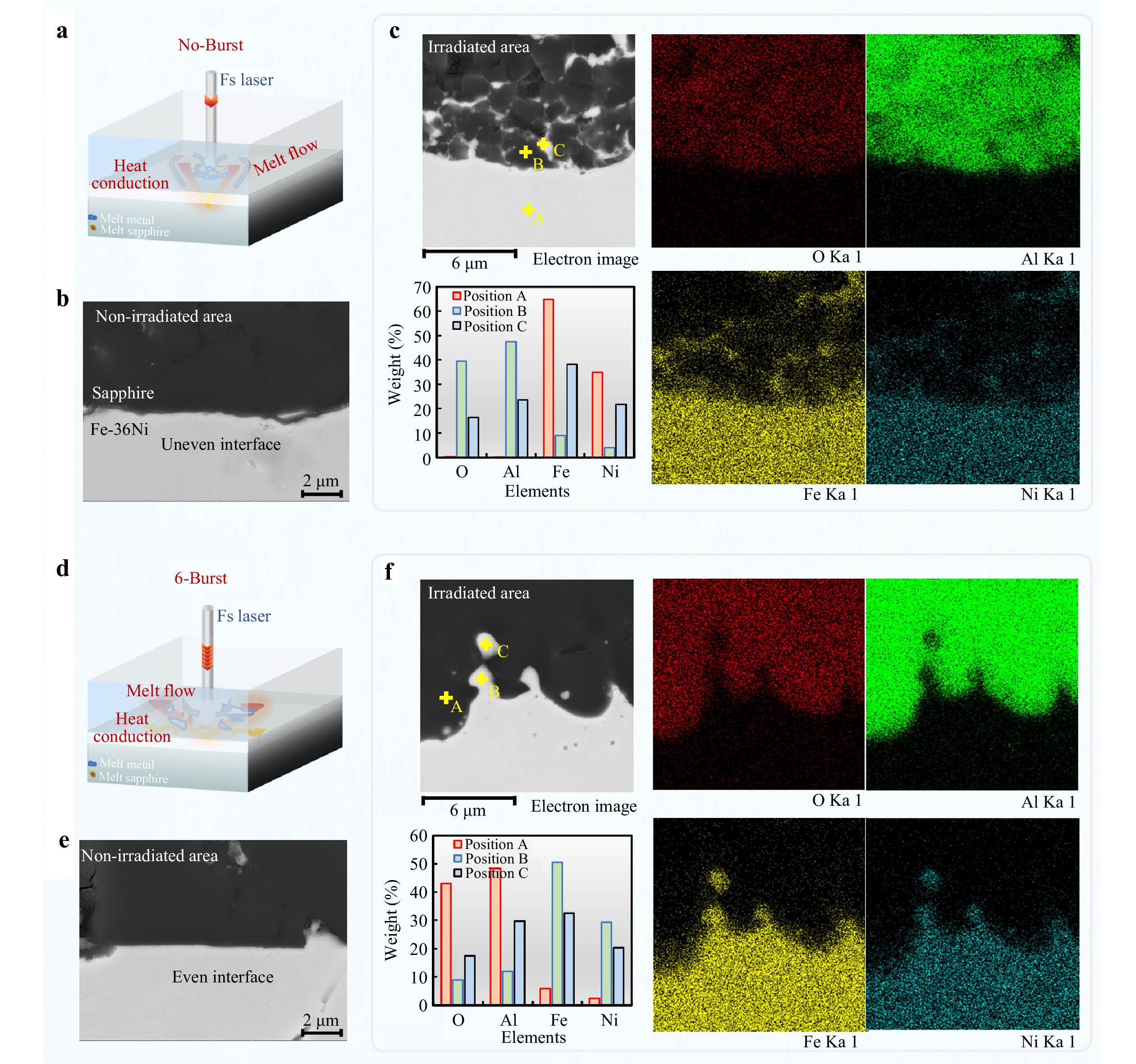
Fig. 3 Interface material bonding behaviour in two welding modes. a Schematic of the femtosecond laser welding mechanism under no-Burst mode. b Non- irradiated area morphology after non-Burst mode femtosecond laser welding. c Interfacial element distribution of no-Burst femtosecond laser welded samples. d Schematic of the femtosecond laser welding mechanism under 6-Burst mode. e Non-irradiated area morphology after 6-Burst mode femtosecond laser welding. f Interfacial element distribution of 6-Burst femtosecond laser welded samples.
The weld morphologies varied under the different laser modes. Under the non-Burst mode, the peak power density of the femtosecond laser was higher, resulting in higher modification depths within the sapphire once a stable welding process was established. Consequently, a larger volume of molten sapphire is generated, which exerts a stronger mechanical force to compress the molten Invar, forming an interlocking joint structure (Fig. 3a). In contrast, under Burst-mode conditions, as the number of sub-pulses within each burst increases, the energy of the individual pulses decreases, making it difficult to sustain nonlinear absorption at higher positions within the interface (Fig. 3d). Consequently, the sapphire modification depth decreased with increasing sub-pulse number and stabilised at approximately 150 μm when the sub-pulse number reached four (Fig. S7 in Supplementary S3, Supporting Information). At this point, the energy absorption at the heterogeneous interface was dominated by the linear absorption in the metal. A balance was established between the enhanced thermal accumulation from closely spaced sub-pulses and the reduced energy per pulse. Furthermore, when the number of sub-pulses increased from 6 to 12, the width of the sapphire penetration into Invar decreased significantly. This behaviour differs from previously reported results for the welding of transparent materials under Burst-mode irradiation. Previous studies have suggested that lowering the peak power of each pulse mitigates excessive plasma heating and enhances the thermal effects in transparent materials through cumulative heating, thus broadening the melt region. However, in the sapphire–Invar system, a smaller molten metal volume was observed with an increasing number of sub-pulses. This indicates that the linear absorption on the Invar surface became increasingly localised as the peak power density of the Gaussian laser beam decreased54.
The post-weld interfacial morphology in the non-irradiated regions further confirmed this observation. Under the non-Burst mode, the higher peak power density allowed a higher volume of Invar to be heated and melted, resulting in disturbed boundaries, even in non-irradiated areas (Fig. 3b). Under the 6-Burst mode, the reduced energy density resulted in a smaller molten zone, and the Invar surface morphology in the non-irradiated regions remained constant (Fig. 3e). Clear interfacial air gaps were observed in these regions, indicating that the volume of the molten Invar was no longer sufficient to fill the interface. Similar phenomena were observed at higher sub-pulse numbers (Fig. S10 in Supplementary S5, Supporting Information).
From the perspective of the interfacial elemental distribution, the non-Burst mode resulted in localised regions rich in Fe and Ni at the interface, enclosed by areas enriched in Al and O, indicating a closed interfacial structure resulting from the laser-induced impact (Fig. 3c, and Fig. S11 in Supplementary S5, Supporting Information). Under the 2-Burst mode, these enriched regions shifted toward the metal side (Fig. S12 in Supplementary S5, Supporting Information). Under the 6-Burst mode, the sapphire–Invar interface showed a more homogeneous distribution of O, Al, Fe, and Ni without enclosed accumulation zones (Fig. 3f, and Fig. S13 in Supplementary S5, Supporting Information). When the sub-pulse number was further increased to 12, the elemental distribution followed a similar trend (Fig. S14 in Supplementary S5, Supporting Information). Elemental mapping of the cross-sectional regions revealed that the interfacial fusion during femtosecond laser welding is dominated by the flow of molten sapphire and molten Invar55. The variations in the impact and absorption mechanisms under different laser modes result in distinct mixing and flow patterns. Fe and Ni were predominant on the metal side of the interface, whereas Al and O were scarcely detected, indicating that no significant material transport or chemical reactions occurred across the interface. Under the non-Burst mode, localised points resembling sapphire in morphology (e.g. point B) contained O and Al as major components but also showed small amounts of Fe and Ni, suggesting partial interdiffusion (Fig. 3c). Similarly, in regions resembling Invar (e.g. point C), Fe and Ni were dominant, accompanied by appreciable amounts of Al and O. The relative elemental proportions at these points closely matched those of the two base materials, indicating physical mixing rather than chemical reactions or the formation of new phases. Even under the 6-Burst mode, similar mutual diffusion behaviours were observed at the interfacial regions (e.g. points A and B) despite the absence of interlocking structures in the SEM morphology. At point C, located farther within the Invar substrate, a noticeable increase in the Al and O contents was still detected, consistent with a moderate degree of mutual fusion (Fig. 3e).
In summary, the interfacial morphologies and elemental distributions indicate substantial differences in the energy deposition behaviour between the two laser modes, resulting in two distinct types of joint formation. The fusion between sapphire and Invar primarily results from the physical intermixing of the molten phases without the formation of new chemical compounds or phases.
-
The femtosecond laser welding process enabled the localised melting of the metallic material, which subsequently infiltrated the joint interface under spatial confinement, achieving non-optical-contact bonding between the Invar alloy and sapphire. This technique relies on a tailored structure of ultrafast laser pulses to induce strong localised absorption, facilitating thermal accumulation at the interface while minimising damage to the surrounding brittle sapphire. As shown in Fig. 4, the SEM and BSE images of the fracture surfaces under different Burst conditions reveal distinct morphologies, demonstrating the influence of the laser parameters on the melting behaviour and weld quality. An important and illustrative feature is shown in Fig. 4a(i), a(ii), where a scratch on the Invar alloy surface (originally rough and deep) is observed on the far left. Notably, this scratch was completely filled and levelled after the laser welding process, resulting in a flat metallic surface. This transformation provided strong experimental evidence that the Burst-mode femtosecond laser welding not only achieved physical bonding but also converted a non-optical-contact interface into an optically flat and continuous joint. This behaviour indicates thorough melting and reflow of the Invar alloy, with effective surface wetting and gap filling, even in microscale surface irregularities.
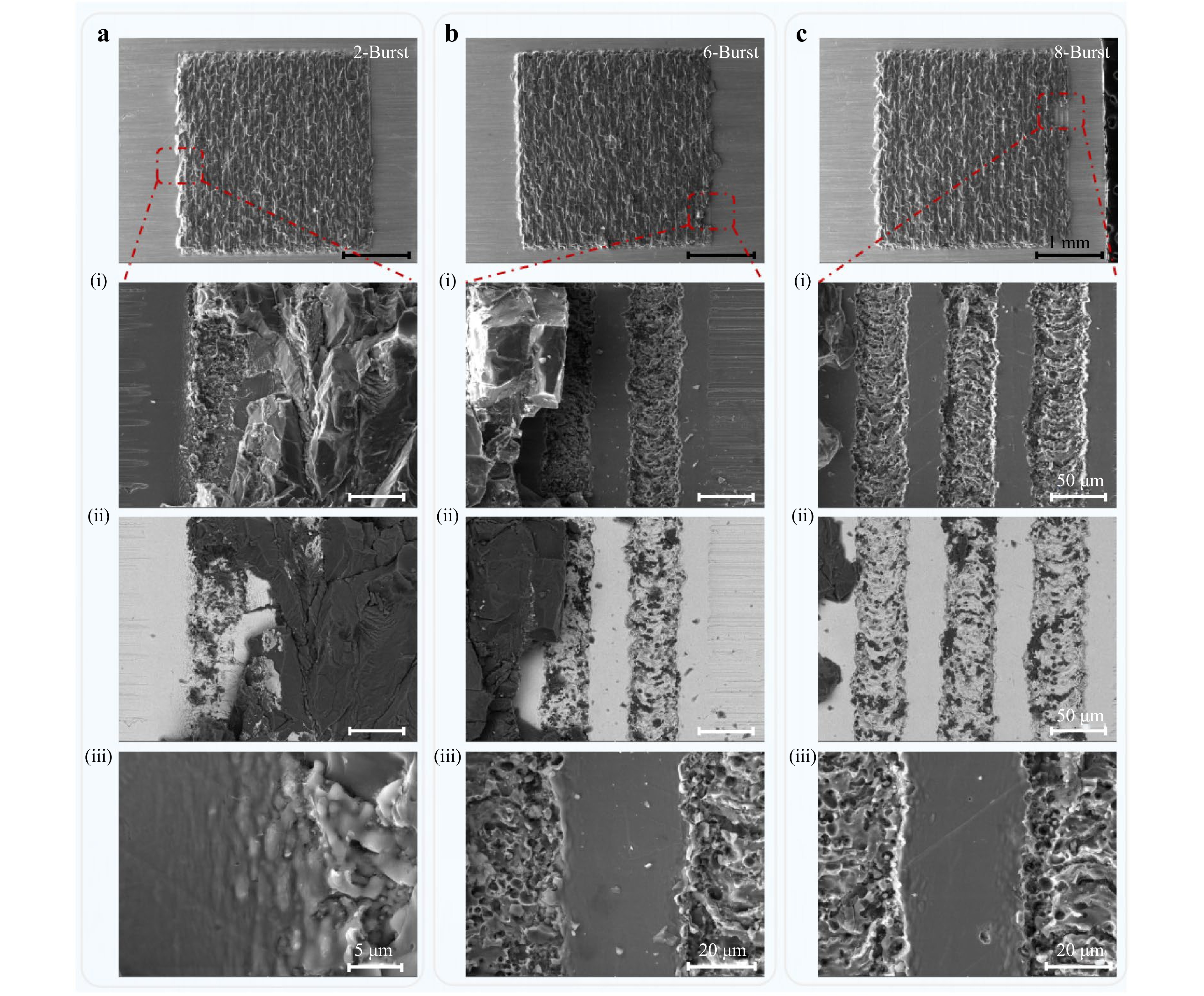
Fig. 4 Fracture surface after laser welding. a 2-Burst, b 6-Burst, and c 8-Burst mode femtosecond laser welding. (i) SEM and (ii) BSE images of the fracture surface morphology on the metal surface of the joint. (iii) Post-melting surface features of the metal under spatial confinement.
The relatively smooth metallic surfaces (Fig. 4a–c(iii)) correspond to the re-solidified Invar alloy, which filled the joint interface during laser welding. These areas indicated that the molten metal achieved good wetting and spreading under spatial confinement. In contrast, the rough and uneven regions (Figs. 4a–c(i, ii)) represent the fracture morphologies after the joint was subjected to shear loading. These surfaces exhibit tear-like features, pore distribution, and typical brittle fracture patterns, distinguishing the original fusion zone from the failure zone and underscoring that although the metallurgical bond is effective, the joint performance is still constrained by material limitations. Notably, the melting width on the metal side exceeds the nominal laser spot size of 33 μm, with the widest region observed under the No-Burst mode, approaching 50 μm. As shown in Fig. S6 (Supplementary S3, Supporting Information)), this width gradually decreased with an increasing number of sub-pulses under the Burst mode. This can be attributed to two factors. First, under the No-Burst mode, the femtosecond laser delivers a higher peak power per pulse, and the Gaussian spatial profile of the beam enables ablation over a broader effective area. Second, the high-repetition-rate pulses induced thermal accumulation, further promoting melting beyond the focused spot size. In contrast, as the number of sub-pulses increase under the Burst mode, the energy per pulse is reduced, resulting in a smaller effective ablation diameter and narrower melting width.
Despite these variations in the interfacial morphology, such as the porosity density, melt depth, and interface flatness, the measured shear welding strengths (Fig. S15 in Supplementary S6, Supporting Information) remained relatively consistent across the 1–12 Burst conditions, ranging from approximately 9 to 13 MPa. This convergence suggested that the joint strength was no longer determined by the metallurgical bond but was instead limited by the brittle fracture behaviour of the sapphire. The fractographic analysis showed that failure occurred on the sapphire side rather than at the metal interface, indicating that the bonding strength exceeded the local cohesive strength of the sapphire substrate. The EDS elemental mapping (Fig. 3) further supports this observation. Under the 6-Burst mode, the interface between Invar and sapphire became more uniform with minor elemental diffusion and a flatter morphology, indicating improved bonding quality. However, despite these interfacial improvements, the macroscopic shear strength did not increase significantly, as it remained constrained by the inherently low fracture toughness of sapphire.
Optical microscopy revealed the presence of distinct cracks within the sapphire substrate, including laterally propagating cracks along the welded interface that were often interconnected as well as vertically oriented cracks aligned with the laser incident direction. These crack morphologies were observed under both the non-Burst mode and across various Burst pulse conditions with different sub-pulse numbers, exhibiting similar structural characteristics without significant differences (Figs. S16 and S17 in Supplementary S6, Supporting Information). This consistent crack pattern, regardless of the laser pulse structure, suggests that thermal-stress-induced damage within the sapphire plays a dominant role in determining the overall joint performance. Despite variations in the laser parameters, the shear strength measurements remained relatively close across different modes, indicating that the strength of the sapphire–Invar alloy welds was primarily constrained by the initiation and propagation of cracks in the sapphire rather than by differences in metallurgical bonding at the interface.
From the perspective of dissimilar-material welding, this underscores a fundamental challenge: the thermal and mechanical mismatch between brittle ceramics, such as sapphire and ductile metals, such as Invar. The localised and rapid heating associated with ultrafast laser irradiation induces steep temperature gradients and thermal stress fields, which are particularly problematic in low-toughness ceramics. These stresses readily exceed the fracture threshold of the sapphire, resulting in the formation of both interfacial and through-thickness cracks. Therefore, although femtosecond laser Burst techniques improve metal-side melting, spreading, and bonding quality, they cannot fully eliminate sapphire-side cracking. Addressing this limitation requires not only process optimisation to reduce the thermal stress intensity, such as through tailored pulse shaping, beam scanning strategies, or preheating, but also material system-level solutions. These include the introduction of compliant interlayers to buffer mechanical mismatches and the use of microstructural modifications (e.g. laser-induced stress-relief patterns) to mitigate crack propagation within the sapphire substrate.
Burst-mode femtosecond laser welding effectively enhances metal melting and interfacial wetting, enabling high-quality heterogeneous bonding under spatial confinement. The observed scratch-filling behaviour and planarisation of the Invar surface provide compelling experimental evidence for the technique’s ability to transform non-optical-contact gaps into optically seamless joints. Although the metallurgical bond quality improved with burst modulation, the overall joint strength was ultimately constrained by the low fracture resistance of sapphire. Future work should explore strategies, such as stress-distributing interface layers or hybrid materials to overcome the inherent brittleness of ceramic substrates.
-
In recent years, laser-welding technologies for transparent and metal-dissimilar materials have rapidly developed, drawing increasing attention from researchers. Depending on whether the sample surfaces were in optical or non-optical contact, two distinct categories with significant differences in the welding performance and welding mechanisms were established, as shown in Fig. 556–63. In optical contact welding, the welding strength of ultrafast laser-welded dissimilar sapphire/stainless steel materials reaches 160 MPa17. Under non-optical contact conditions, a welding strength of 17.19 MPa was achieved with a surface roughness Sa of 0.599 μm22. In this study, a welding strength of 11.73 MPa was obtained between sapphire and Invar alloy with a surface roughness Sa of 2.128 μm (8-Burst mode). The optical-contact condition produced a confined interface space, whereas the non-optical-contact condition created a free interface space. These differences in the interface environment resulted in significant differences in the welding mechanisms and affected welding performance.
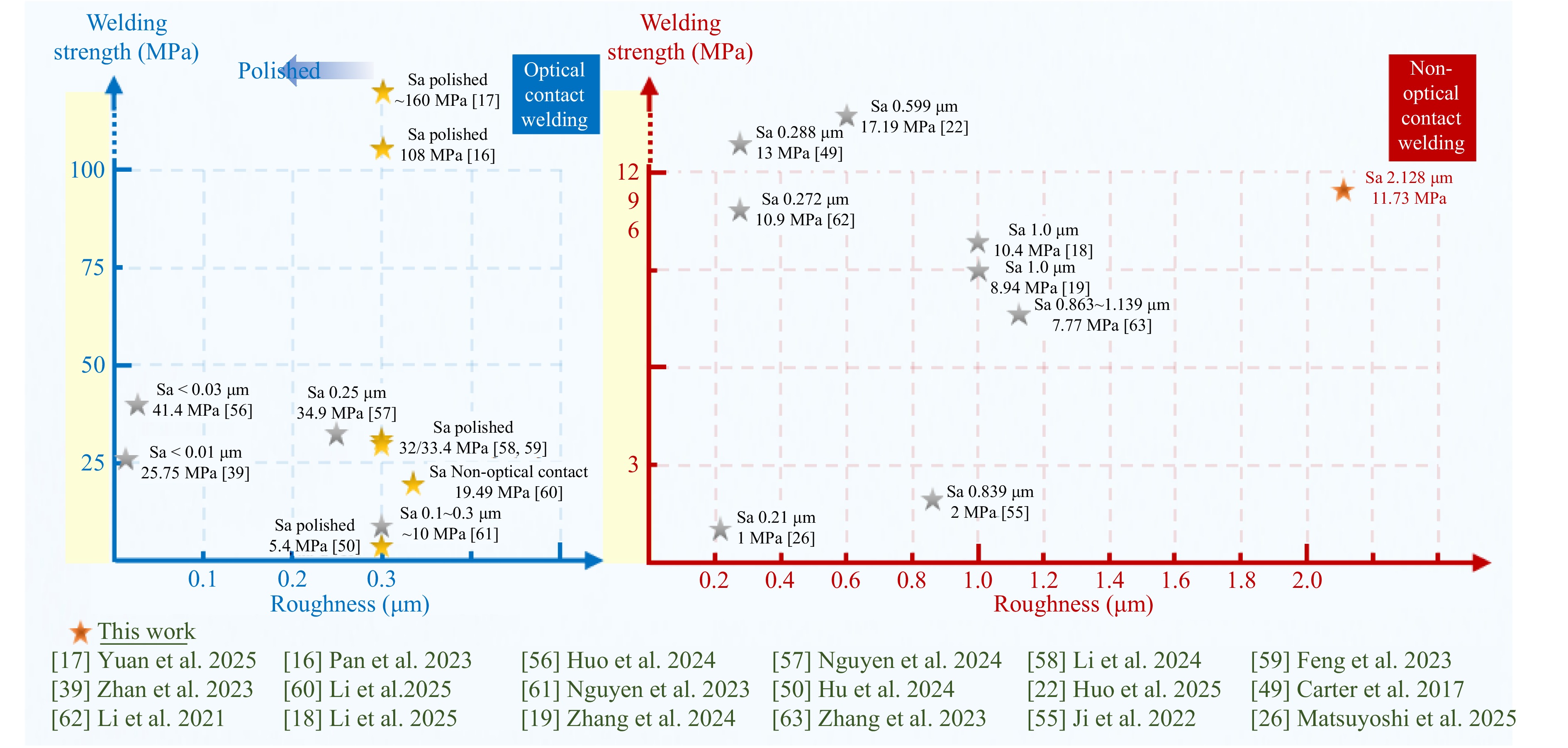
Fig. 5 Comparison of ultrafast laser welding performance for transparent-metal heterogeneous materials.
Based on the high-speed plasma imaging results and smooth fracture surfaces observed on the joints, our study concludes that, despite significant scratches on the initial metal surface, the welding conditions corresponded to non-optical-contact welding. However, under the influence of ultrafast laser irradiation with a high repetition rate, the metal melt can spread freely across the interface, thereby facilitating the transition from non-optical contact welding to optical contact welding. Nevertheless, owing to the stress constraints from the modified region on the sapphire side, the final welding strength still exhibited a significant difference compared with that of typical optical contact welding. Therefore, it can be concluded that during the welding of rough metal materials with transparent materials, the total laser energy deposited within the transparent material plays a decisive role in determining the welding strength.
In a recent study, Yuan et al. reported that controlled laser energy injection enabled melting of stainless steel at the interface while maintaining sapphire in a solid state. Welding strengths as high as 160 MPa were achieved by relying on the diffusion and mixing of elements at the interface. By optimising the laser energy deposited within the sapphire, this method effectively suppresses the generation of stress and cracks on the transparent material side, thereby significantly improving the welding performance17. Based on this approach, compared to non-optical contact welding, optical contact welding positioned a heterogeneous interface within a confined space. When the laser irradiated the interface and generated the metal plasma, the free expansion and growth of the plasma were significantly restricted, resulting in a higher temperature and density. Because of the narrow air gap, the transparent material was closely attached to the metal. Through this mutual promotion, the laser energy required for simultaneously heating the metal and transparent material was significantly reduced compared to that required for non-optical contact welding. Consequently, the laser energy deposited within the transparent material and the subsequently induced stress were effectively controlled, enabling welding with higher strength.
From this perspective, the welding strength of non-optical-contact dissimilar materials is inherently limited. Improving the interface absorption through spatiotemporally shaped laser beams, such as the Burst mode welding proposed in our study, is insufficient to fundamentally enhance the welding strength of dissimilar materials. In this context, based on our experimental observations, an important phenomenon in the ultrafast laser welding of dissimilar materials is the transformation of a non-optical-contact interface into an optical-contact interface driven by the spontaneous flow of molten metal into the interfacial gap. This mechanistic insight offers several promising directions for future research. For example, the pretreatment of metal surfaces, such as ultrafast laser polishing, can reduce surface roughness and promote better contact conditions before welding64. The introduction of intermediate layers, particularly flexible or deformable materials, may help bridge the initial gap and facilitate the contact transformation65. In addition, applying localised continuous-wave laser heating can induce metal melting and thermal expansion, further improving interfacial conformity66,67. Furthermore, we identified that the formation of internal cracks on the sapphire side was a key factor limiting the joint strength under burst-mode spatiotemporal shaping. This observation suggests the necessity for postprocessing strategies. For instance, laser annealing can be explored as a means to heal microcracks in transparent materials and improve the structural integrity of joints.
Therefore, our study reveals the dynamic welding mechanism of non-optical contact transparent/metal dissimilar materials, highlighting the active interface regulation process during welding. Although the free space at the interface can be modulated into an optical contact state under an appropriate laser energy injection, the laser energy deposited within the sapphire remains excessively high, resulting in elevated stress levels that limit the achievable welding strength. Although optimising the spatiotemporal distribution of the welding laser, such as through Burst mode modulation68,69, can yield certain improvements, it remains difficult to fundamentally address the stress issue within the sapphire and significantly enhance the welding performance.
-
Considering the broad application potential of transparent/metal dissimilar material joining, achieving high-performance connections under non-optical-contact conditions, that is, between rough metal surfaces and transparent materials, has become an inevitable development trend. Before our study, the welding mechanism of non-optical contact dissimilar materials remained unresolved, and the technical bottlenecks limiting the welding performance were unclear. This study systematically investigated the welding mechanism, performance limitations, and interface behaviour of femtosecond laser joining of rough Invar and sapphire. The main conclusions are as follows.
(1) Direct visualisation of the welding process: utilising continuous high-speed imaging with a spatial resolution better than 2 µm and a temporal resolution of approximately 111 µs, we revealed for the first time the dynamic femtosecond laser welding process of sapphire-Invar joints under non-optical-contact conditions. Despite a surface roughness (Sa) of 2.128 µm, a welding strength of 11.73 MPa was achieved.
(2) Mechanism of interface transformation and strength generation: Laser-induced molten metal flow actively fills the interfacial gaps, dynamically converting the interface from a non-optical contact to an optical contact. The compressive forces from the molten sapphire further drive the lateral spreading of the Invar melt, contributing to the interfacial bonding strength.
(3) Crack-limited performance and implications for process design: Excessive energy input causes stress-induced cracking within sapphire, thereby limiting the ultimate strength. Although Burst-mode modulation improved the interface uniformity, it could not suppress brittle fracture in the sapphire. These findings provide mechanistic insights and a methodological basis for enhancing the joint performance in non-optical-contact systems.
-
Materials: The materials used in this study were sapphire and Invar alloy (Fe-36Ni). For welding strength testing, specimens with dimensions of 8 × 10 × 2 mm for sapphire and 10 × 20 × 2 mm for the Invar alloy were employed. To facilitate cross-sectional sample preparation and observation, smaller specimens with dimensions of 5 × 10 × 2 mm were selected for welding and subsequent analyses. The surface roughness (Sa) of the sapphire was 1.464 μm, whereas that of the Invar alloy was 2.218 μm (Fig. S1 in Supplementary S1, Supporting Information).
Femtosecond laser welding system: Femtosecond laser welding system: A femtosecond laser (HR-Femto-IR-400-60, Huaray, China) with a wavelength of 1035 nm and a pulse duration of 238 fs was used to conduct the welding experiments. The femtosecond laser was operated at a repetition rate of 200 kHz under all Burst modes, with an interval of 22 ns between the sub-pulses within each Burst. Two irradiation modes were employed in the process experiments: a single-pulse mode with a pulse energy of 132.5 μJ, and a multi-pulse (Burst) mode comprising 1 to 12 sub-pulses, with a total energy maintained at 132.5 μJ. The laser beam was focused using an f-theta scanning lens with a focal length of 80 mm, resulting in a spot size of approximately 30 μm. During welding, the focal point of the femtosecond laser was positioned at the centre of the heterogeneous interface, and a dedicated clamping fixture was used (Fig. S18 in Supplementary S8, Supporting Information). Under clamped conditions, the interfacial gap between samples was measured to be approximately 7–8 µm. A zigzag scanning pattern was adopted over a welding area of 3 × 3 mm, with a line spacing of 80 μm and scanning speed of 40 mm/s. The relevant parameters are listed in Table 1.
Parameters Parameters Wavelength 1035 nm Scanning speed 40 mm/s Pulse duration 238 fs Spot size 33 μm Repetition rate 200 kHz Welding area 3 × 3 mm Burst configuration 45 MHz
1–12 sub-pulsesPulse energy Burst total: 132.5 μJ Table 1. Welding parameters
High-speed plasma imaging: A high-speed imaging system was established to capture the welding process using a stationary laser beam and moving sample. A 10× objective lens was used to image the femtosecond laser welding region, and the plasma radiation emitted from the interface during welding was recorded by a high-speed camera (FASTCAM NOVA S9, Photron, Japan), achieving a spatial resolution better than 2 µm. The frame rate was fixed at 9000 fps, resulting in a temporal resolution of 0.11 ms. The focusing lens for the femtosecond laser had a focal length of 80 mm, and during the welding process, the translation stage was set to move at 40 mm/s, consistent with the scanning speed used in Femtosecond laser welding system.
Characterization of Static Observations: The microstructures and chemical element distributions of the weld joints were characterised using a scanning electron microscope (SEM, MIRA4 LMH, TESCAN) equipped with an energy-dispersive spectrometer (EDS, One Max 50). Cutting, grinding, and polishing were performed to obtain the exact profile of the sample.
-
We are grateful for financial support from the National Key R&D Program of China (Grant No. 2023YFB4605500), National Natural Science Foundation of China (Grant No. 52105498), State Key Laboratory of Ultrafast Optical Science and Technology (Grant No. 2025SKL-uFAST-KF22), State Key Laboratory of Precision Manufacturing for Extreme Service Performance (Grant No. ZZYJKT2023-08 and Kfkt2024-16), Science and Technology Innovation Program of Hunan Province (Grant No. 2021RC3074), the Key Program for Basic Research (Grant No. JCKY2023210A005 and JCKY2024210A001), and Changsha Natural Science Foundation (kq2402089).
Tailoring sapphire–invar welds using burst femtosecond laser
- Light: Advanced Manufacturing , Article number: 3 (2026)
- Received: 21 June 2025
- Revised: 04 November 2025
- Accepted: 06 November 2025 Published online: 29 January 2026
doi: https://doi.org/10.37188/lam.2026.003
Abstract: Abstract. The efficient and robust joining of transparent metal-dissimilar materials remains a significant challenge in high-performance system integration. A primary barrier is the inherently rough surfaces of metals, which hinder reliable bonding with transparent materials, largely due to the limited understanding of the underlying welding mechanisms. In this study, we demonstrate ultrafast laser joining between sapphire and metal substrates with surface roughness (Sa) up to 2 μm, achieving a maximum shear strength of 11.73 MPa. High-speed imaging techniques were employed to conduct the first systematic investigation of coupled absorption dynamics at heterogeneous interfaces. The plasma ejection observed during welding indicated that the molten metal actively confined the interfacial region, transforming the initial free space into a confined space. This transition facilitates the formation of an optical contact condition, significantly improving the joint strength. To further explore the potential of pulse shaping in controlling interfacial behaviour, the effects of temporal shaping (Burst mode) on laser energy deposition, joint strength, and interfacial morphology were examined. Consistent joint quality was achieved across a range of burst parameters, with shear strengths ranging from 9 to 13 MPa. Fractographic analysis indicated that the fracture was predominantly governed by the internal stress within the sapphire, thereby limiting further improvements in joint strength. The revelation of the ultrafast laser welding mechanism for non-optical contact dissimilar materials, along with the exploration of temporal shaping for enhancing welding performance, offers theoretical insights and technical guidance for the development of high-performance heterogeneous material joining.
Research Summary
Ultrafast Laser Welding of Dissimilar Materials: New Insights and Enhanced Performance
Efficiently joining dissimilar materials, such as transparent sapphire and metal alloys, is crucial for high-performance system integration. However, surface roughness often hinders reliable bonding. Cong Wang and colleagues from Central South University have developed an ultrafast laser welding technique that successfully joins dissimilar materials under non-optical contact conditions, achieving a shear strength of 11.73 MPa. By employing high-speed imaging, the team provided the first systematic observation of the welding process under non-optical contact conditions, revealing how laser-induced molten metal flow fills the interface gap, transitioning the bond from non-optical to optical contact. This process significantly improves joint strength. The study also explores the role of Burst-mode laser shaping, offering new strategies for robust, high-performance material integration.
Rights and permissions
Open Access This article is licensed under a Creative Commons Attribution 4.0 International License, which permits use, sharing, adaptation, distribution and reproduction in any medium or format, as long as you give appropriate credit to the original author(s) and the source, provide a link to the Creative Commons license, and indicate if changes were made. The images or other third party material in this article are included in the article′s Creative Commons license, unless indicated otherwise in a credit line to the material. If material is not included in the article′s Creative Commons license and your intended use is not permitted by statutory regulation or exceeds the permitted use, you will need to obtain permission directly from the copyright holder. To view a copy of this license, visit http://creativecommons.org/licenses/by/4.0/.

 DownLoad: