


-
The remarkable properties of THz waves have inspired the development of numerous emerging applications. High frequencies present the potential for enhanced channel capacities in 6G and beyond wireless communications. The long-wavelength electric dipole vibrations of many molecules and crystals are in the THz range, making a wide range of applications possible in chemical identification, material characterisation, atmospheric/astrophysics studies, and gas sensing1−5. Owing to its non-ionising nature, THz radiation is a powerful tool for non-destructive control6, security screening7, weapon detection8, biomedical imaging9, and delicate investigation of cultural heritage artifacts10.
Due to the broad applicability of THz radiation, efforts have been made to improve the performance of optical elements to meet the demands of THz applications. The most common lens- or mirror-based THz focusing systems have limited focal spot quality and energy efficiency or provide a trade-off between these two important parameters11. One of the current trends in optical element design is the reduction in thickness11. Historically, aberrations have been corrected with aspheric shapes or multilens designs, leading to heavy and complex systems12−14. Consequently, the development of ultra-thin lenses is crucial, and Fresnel zone plates (FZPs) are a viable solution. Despite advances in diffraction optics, most FZPs remain non-switchable. However, for emerging applications, such as computational THz imaging and sensing15, light detection and ranging16, and dynamic holography, it would be desirable to control the optical elements.
From this point of view, significant improvement of the THz optics performance has been achieved by the electrical tunability of nanomaterial properties. Among the various techniques, electrochemical gating paves the way for the gating of porous bulk nanomaterials. For example, ionic-liquid gating on a graphene modulator has shown an improved amplitude modulation depth of up to 99% in the transmission mode under an applied voltage as small as +3 V17. By controlling the electrolyte–graphene interface gap in the quarter-wavelength cavity structure and utilising the resonance effect, a 40% modulation depth was reached in the reflection mode in the [−0.5, +0.5] V range18. In these studies, the ionic liquids created an electrical double layer at the graphene interface, which could adjust the intraband transition of carriers, even under a small applied bias. Similarly, carbon nanotubes, graphene counterparts, show a Fermi level shift of over 1.2 eV, even at low biases (~ 3 V)19. The combination of strong electrostatic doping of single-walled carbon nanotubes (SWCNTs) with their intrinsically high conductivity20 opens a new direction for device improvement. However, to the best of our knowledge, the potential of SWCNT films as electrochemically tuned THz optoelectronic devices has not been discussed or considered in previous studies.
In this study, we manipulated the intensity of the beam that passes through a transmission type THz SWCNT-based FZP with active ionic-liquid gating. This is possible owing to advanced technologies. for nanotube production and patterning combined with ionic-liquid gating. To predict the FZP performance, we first performed spectroscopy of the separate conventional ionic-liquid gating cell. The gating of SWCNT films led to a two-fold increase in their refractive index upon change of the bias voltage from –2 to +2 V. Next, we employed a new and robust chemical-free method for the deposition of patterned carbon nanotube films for dry transfer onto a z-cut quartz substrate. Our FZP with nanometer thickness showed intense focusing efficiency with a diffraction-limited lateral size of 1.14λ. The encapsulation of FZP in an electrochemical cell enabled the tuning of the FZP focal spot intensity from −20 to +15%. This approach suggests a new direction for the design of SWCNT-based THz optics.
-
Fig. 1 shows a schematic design of the proposed tunable lens. The lens comprised a thin SWCNT film, FZP, with an ionic liquid sandwiched between two z-cut quartz substrates. The expression for the zone is as follows: $ r_n^2+f^2=\left(f+n({\lambda}/{2})\right)^2 $, where $ n $ is the zone number, $ r_{n} $ is the outer radius of the n-th zone, $ f $ is the focal distance, and $ \lambda $ is the working wavelength. For a practical implementation, we engineered an FZP with a focal length of 2 cm and $ N=10 $ at $ \lambda=917 $ $ \mathrm{\mu m} $ ($ \nu=327 $ GHz). The lens is 28.6 mm in diameter and consists of five concentric rings. The lens size was chosen to cover the full width of the beam and avoid fabrication limitations (see SI S4 for details). The same lens could be used at both higher and lower frequencies. At higher frequencies, the focus point was extended. For 300 $ \mu $m (1 THz) the focus will be at 6.2 cm, for 150 $ \mu $m (2 THz) at 13 cm and for 100 $ \mu $m (3 THz) at 19.5 cm. Interconnections through small stripes ensured a uniform doping distribution. To enable dynamic electrical control of the lens properties, four arc-shaped contacts were deposited using thermal evaporation, consisting of a 5 nm layer of titanium and a 50 nm layer of gold. Two of these electrodes were connected to the SWCNT FZP, whereas the remaining two served as counter electrodes for gating. The ionic liquid utilised was 1–Butyl–3–methylimidazolium bis (trifluoromethylsulfonyl) imide (BMIM NTf2), which was chosen for its large electrochemical window of stability and tolerance to the ambient atmosphere. Patterned films for the FZP were fabricated via aerosol chemical vapour deposition21. SWCNTs serve as opaque regions in the FZP design22, 23. The fabrication process involves laser-etching a stainless-steel plate to create a 150−200 $ \mu $m stencil, which is then pressed onto a nitrocellulose filter using rollers to selectively compress the areas. The SWCNT aerosol was then deposited onto uncompressed filter areas, creating a nanotube film that matched the stencil geometry, followed by a dry transfer onto a quartz substrate24.
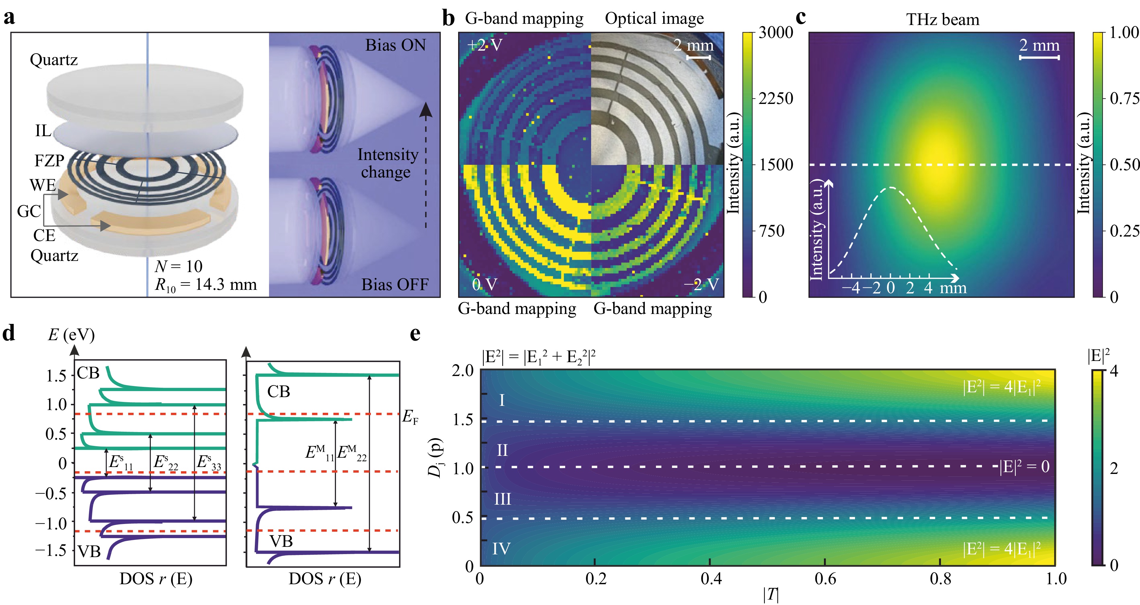
Fig. 1 a Concept of the device structure. A thin ionic liquid layer coats a thin Fresnel zone plate based on SWCNT encapsulated between two z-cut quartz substrates and connects to the FZP with two gold contacts (GC). The working and counter electrodes are denoted as WE and CE, respectively. The FZP consists of 10 zones, with an external radius of 14.3 mm. Gate-induced change of the dielectric properties of the carbon nanotube film results in the change of the radiation intensity in the FZP focus. b The photo of the fabricated SWCNT FZP (upper right corner) alongside Raman intensity maps at applied voltages of +2, 0, and −2 V (at the G-mode frequency corresponding to each voltage). The opaque zones in the optical image are SWCNTs. c The THz spot without FZP measured with a Golay cell and shown in normalised units. d Electronic properties of semiconducting (left) and metallic (right) SWCNT, each with an approximate diameter of 2 nm. VB denotes valence band, CB represents conduction band, and DOS denotes density of states. The estimated maximum and minimum shifts of the Fermi level are highlighted with dashed red lines. e The interference of two coherent beams calculated to understand the role of amplitude and phase modulations.
Fig. 1a (right-hand side) illustrates the basic concept of the proposed flat FZP, in which the applied voltage tunes the intensity of the focal spot intensity. When a uniform plane wave radiated through the FZP, part of the incident radiation was partially blocked (absorbed and reflected) by the SWCNT zones, experiencing both amplitude and phase modulation. Fig. S9 shows that the phase modulation under ionic gating is negligible (< 5°), whereas the amplitude changes dominate. Focusing is the result of the constructive interference (in the focal plane) originating from different Fresnel zones. Under these conditions, amplitude modulation makes a substantial contribution to the focusing performance, making the amplitude FZP rather than the phase. In our case, the focal spot intensity at the shadow side of the lens was reached owing to the alteration of the effective SWCNT refractive index, whereas the refractive index of the ionic liquid remained unchanged (Fig. S1). This modification is possible because of the adjusted intraband transition appearing under small applied biases when a large double layer is formed at the interface of the ionic liquid and SWCNT rings. The difference in the complex refractive indices between the transparent regions and those filled with SWCNT is substantial, resulting in a minimum phase change, which is necessary for constructive interference (regions I and IV in Fig. 1e) and region IV in Fig. S825.
In our study, we utilised Raman microscopy (Setup details present in the Experimental section) to explore the gate-tunable response of SWCNT films. The spectral profile and frequency of the Raman-active G band are known to be sensitive to variations in the Fermi energy26. By recording the G-mode intensity (at the G-mode frequency corresponding to each voltage) across the entire active region of the device, both with and without applied voltage, we gained insight into the doping-level distribution. Fig. 1b (top right corner) presents an optical image of the fabricated FZP alongside the Raman maps at applied voltages of +2, 0, and −2 V (top left, bottom left, and bottom right corners, respectively). The application of voltage led to a notable suppression of the intensity compared with 0–V, with a nearly uniform distribution across the FZP area. The observed differences in the Raman map intensities from +2 to −2 V are attributed to the intrinsic downshift of the Fermi level, likely owing to the oxygen-induced p-doping that naturally occurs under ambient conditions27. Further changes in voltage led to the displacement of the Fermi level downward or upward in metallic and semiconducting SWCNTs, depending on the sign of the voltage (Fig. 1d. Literature indicates that for the classical rectangular scheme used in our measurements, each 1 V shift alters the Fermi level by 0.45 eV19. In our case, the samples are already p-doped due to the oxidation that naturally occurs in air, which shifts the Fermi level by 0.1 eV towards the valence band. Therefore, we expect that for the voltage range of [−2; +2] V, there will be a variation of the Fermi level from −1.2 to 0.8 eV (red lines in Fig. 1d).
The experimental verification of the produced THz FZP lens functionality was performed using the custom-made THz continuous-wave imaging setup. As the THz source, we employed a backward wave oscillator (BWO) operating at a frequency of 327 GHz (Fig. 1c) (further details of the experimental setup can be found in the Experimental section). Our specific beam waist selection represents a carefully considered compromise. A wider beam interacts more strongly with the radial gold electrodes in our device architecture, introducing unwanted effects. Conversely, positioning these electrodes at greater radial distances to accommodate a larger beam would diminish the electrochemical doping efficiency because of the increased separation between the electrodes and active regions of the FZP. We would like to highlight that two samples were studied in this work: the ionic-liquid-gated cell and the ionic-liquid-gated FZP, working as tunable lenses. The ionic-liquid-gated FZP geometry is more complex. However, they retain the performance of conventional electrochemical cells. For simplicity, we refer to it as the “ionic-liquid gated FZP” rather than the "ionic-liquid gated FZP cell”.
-
To underscore the significance of the changes in the SWCNT dielectric response during the operation of the flat lens based on FZP, we conducted separate spectroscopic measurements of continuous carbon nanotube films using THz Time-Domain Spectroscopy (THz-TDS). Electrochemical gating was achieved using the distinct two-electrode cell configuration shown in Fig. 2. This device consists of two z-cut quartz substrates filled with an electrolyte (ionic liquid). Gold strips were employed to bias a SWCNT film electrode with a 5 × 10 mm2 film electrode. Upon applying a bias voltage between the sample and counter electrode, positive and negative ions (depending on the voltage sign) from the electrolyte accumulate near the SWCNT film, forming an electric double layer.
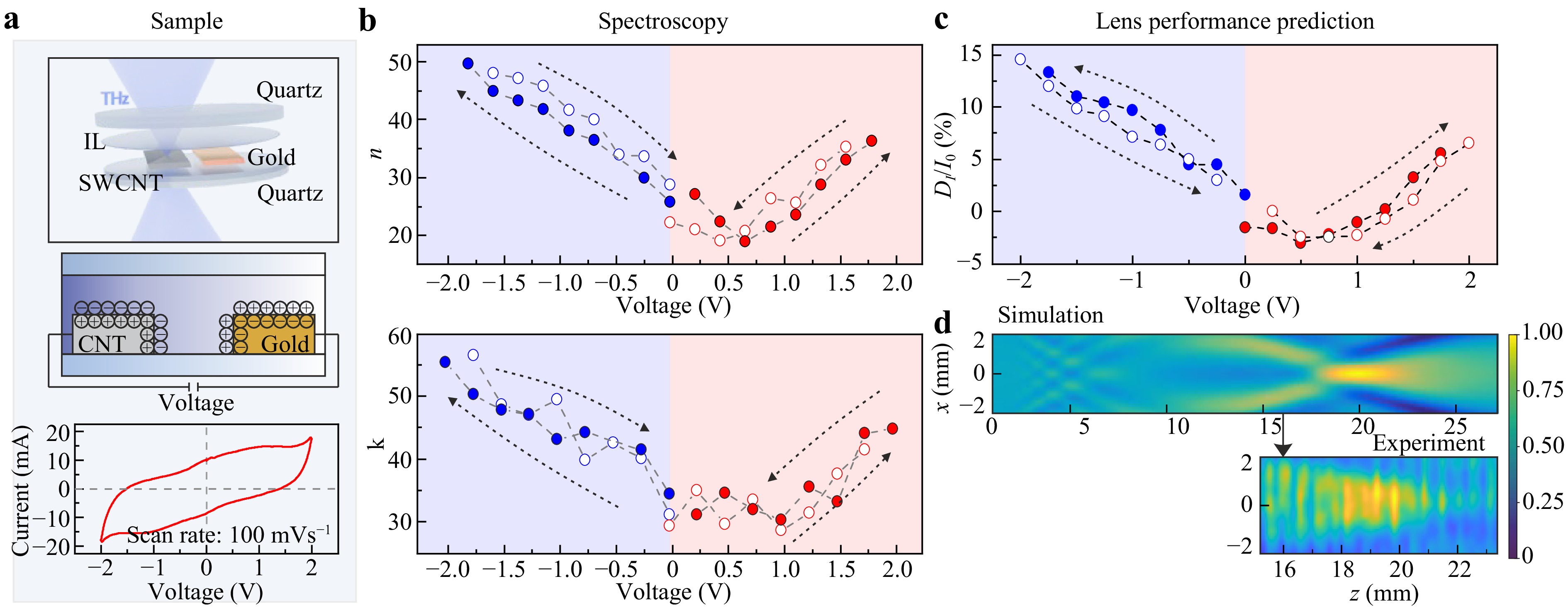
Fig. 2 a From top to bottom: schematic view of the gated SWCNT film in an electrochemical cell; scheme of the operational principle of the ionic-liquid gating inside an electrochemical cell-charged molecules screen the Coulomb potential of SWCNT film and gold pad; results of the cyclic voltammetry studies of the SWCNT films recorded at v = 100 mV/s. b The effective refractive index change of SWCNT films over the voltage range of [−2, +2] V (same as in cyclic voltammetry). The direction of the voltage sweep is denoted by arrows. Solid circles represent the forward direction and hollow circles-backward direction. c The modulation depth of the lens intensity, extracted from simulation, is plotted versus voltage. d The field intensity at 327 GHz transmitted behind the designed Fresnel zone plate in the case of a simulation and experiment at 0 V.
To assess the cell performance, cyclic voltammetry tests were performed at the scan rate of 100 mV/s over the potential range from −2 to 2 V (Fig. 2b, c). A constant potential was maintained for 3 min until a steady-state current was reached, and optical measurements were conducted. The dependence of the real $ n $ and imaginary $ k $ parts of the effective refractive index of SWCNT in the cell on the bias voltage is shown in Fig. 2b. This voltage-induced change can be understood through three possible band alignment scenarios. In the first case, without a gate voltage, the Fermi level was slightly below the neutral point, indicating p-doping due to oxygen or water adsorption under ambient conditions. This was manifested in our experiments by the shift of the refractive index minimum towards positive values. To adjust the Fermi level to a neutral point, it is necessary to apply voltages of +0.5 to +1 V, depending on the specific position in the cyclic voltammetry. In the second scenario, the application of positive voltages effectively shifts the Fermi level toward the conduction band. In the third scenario, the application of negative voltages resulted in a shift in the opposite direction, moving the Fermi level toward the valence band. With the shift in the Fermi level from the neutrality point, the free carrier density in nanotubes increases, leading to enhanced intraband optical absorption.
The pronounced hysteresis loops observed in cyclic voltammetry are mirrored in the behaviour of the effective refractive index of SWCNT in the cell. Two local minima, approximately +0.5 and +1 V, were apparent in both the forward and backward sweeps within the positive voltage regime. This illustrates a distinct difference in the Fermi level positions when the same voltage is applied in both the forward and reverse directions. Fig. 2c shows the transmitted intensity simulating the focusing performance of a hypothetical lens based on FZP, which has an effective refractive index of SWCNT in the cell extracted from spectroscopic measurements. The simulated focus position at 20 mm matched the experimental position well. Using the effective refractive indices of SWCNT in the cell over the whole voltage sweep, we calculated the relative change of the intensity as $ \Delta I/I=[I(V)-I(V=0)]/I(V=0) $ (Fig. 2c). If $ I(V) \gt I(0) $, the MD is positive, indicating an increase in intensity. If $ I(V) \lt I(0) $, the MD is negative, indicating a consequent decrease in intensity. The intensity modulation in the focus position exhibited hysteresis behaviour, which reflected the refractive index change under the applied voltage. Overall, the modulation from approximately −5 to +15% demonstrates the benefit of integrating ionic-liquid gating in the SWCNT FZP.
To illustrate the voltage-dependent THz optical properties, we performed THz imaging of a cloverleaf structure coated with our SWCNT films (Fig. 3a). We observed a significant decrease in the transmission (CNT films on their own) as the voltage was varied toward +2 or −2 V, which manifested as a gradual suppression in the detected reflection mode intensity. The densely packed structure of the SWCNTs combined with their high refractive index allowed for a remarkable amplitude transmission of 0.7 at 0 V, even with a film thickness of 40 nm. We calculated the frequency-dependent EMI shielding efficiency, defined as $ SE=-20log_{10}({ \left | E_{sample}\right |}/{\left | E_{reference} \right |}) $, where $ \left | E_{sample}\right | $ is the amplitude of the signal through the sample and $ \left | E_{reference} \right| $ is the amplitude of the signal from the reference. As the voltage changed, we observed a two-fold reduction in transmission, leading to a four-fold increase in the effectiveness of the electromagnetic shielding, which ranged from 2 to 8 dB at 1 THz (Fig. 3c). Considering the density $ \rho $ of the SWCNT films at 2.4 mg/cm3 36 and thickness $ d $ of 40 nm, we calculated the ASE as $ ASE=SE/ (\rho d) $ of these aerosol-grown SWCNT films at the same frequency (Fig. 3d). Notably, the ASE values for these films were significantly higher than those reported for most other nanomaterials (Fig. 3e). The highest value of approximately 109 dB cm2 g−1 is achieved at −2 V of gate voltage. This result is three orders of magnitude greater than that observed for graphene–PMMA composites owing to their high conductivity. This enhanced shielding effectiveness signifies that lightweight, low-thickness SWCNT films hold substantial promise for applications in high-performance electromagnetic shielding in the THz range.
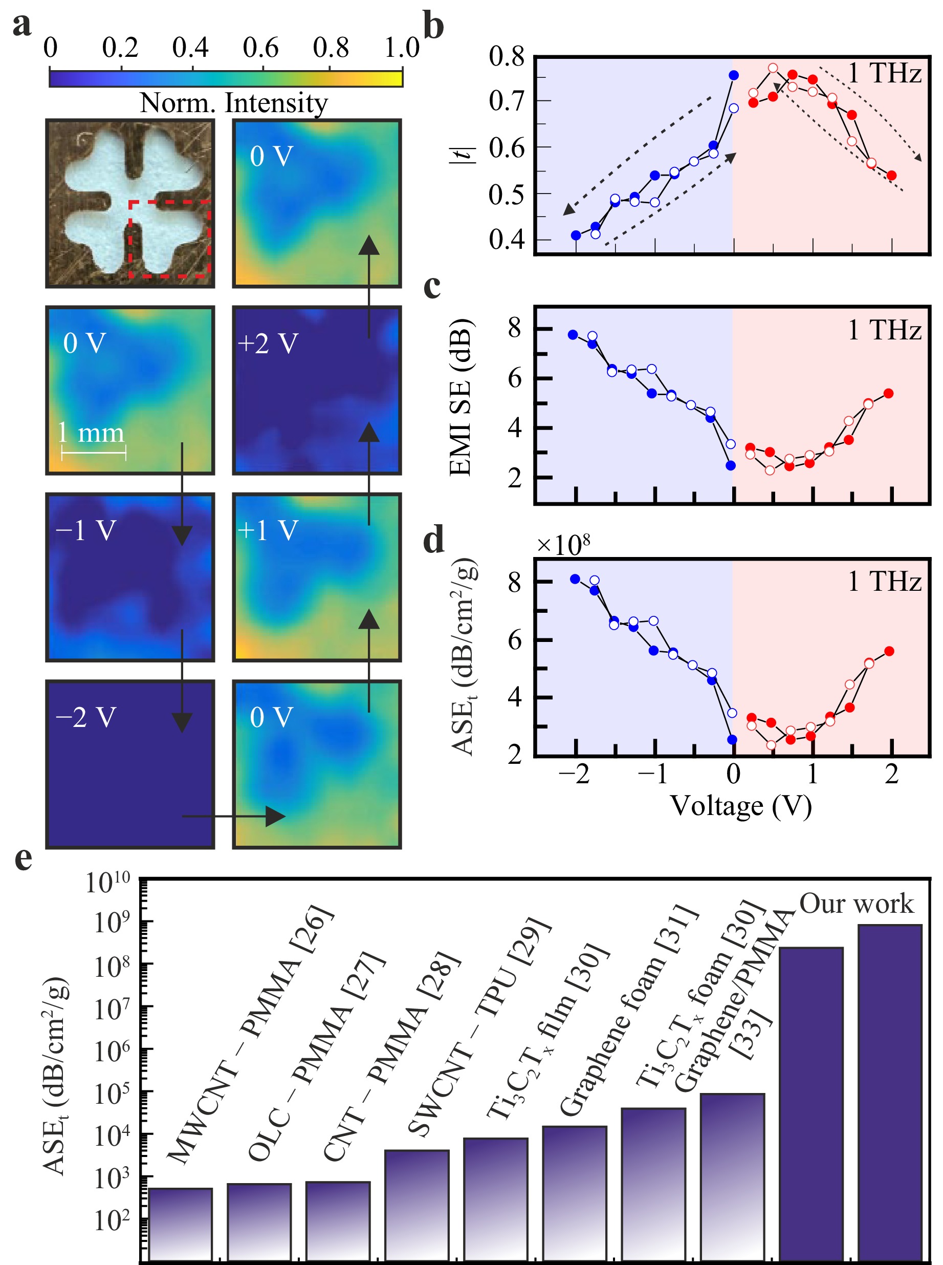
Fig. 3 The optical image (in the left corner) and the THz image of the metallic cloverleaf, which is covered by a SWCNT ionic-liquid cell. The cell is comparable in size to the beam. These images were obtained under an applied voltage that varied from −2 to +2 V. The THz images collected in reflection mode correspond to the area indicated by the red square in the optical image. Importantly, the metallic area around the cloverleaf reflects the THz radiation, which is also modulated by the CNT modulator. The same scale bar is used for all images. b The amplitude of the transmission change of SWCNT films on their own (without cloverleaf) over the voltage range of [−2, +2] V. c and d The corresponding electromagnetic interference shielding effectiveness (EMI SE) and absolute shielding effectiveness (ASE) calculated from (b). e Comparison of the ASE with reported CNT, Graphene, MXenes nanocomposites taken from literature28−35. Last two columns highlighted the results from our work for +0.5 and −2 V. MWCNT–multi-walled carbon nanotubes, OLC–onion-like carbon; PMMA–poly(methyl methacrylate), TPU–thermoplastic polyurethane.
-
Encouraged by the significant tunability of the refractive index, we fabricated an SWCNT FZP using the proposed design framework. Initially, we evaluated the performance characteristics of the FZP by applying a voltage bias ranging from −2 to +2 V in a cyclic voltammetry setup (Fig. 4a). We conducted experimental measurements of beam intensity at 327 GHz. The observed asymmetric intensity behaviour (Fig. 4b) closely resembles the calculated response depicted in Fig. 2c. No difference was observed when the voltage was applied in clockwise and counterclockwise voltage sweeps (Fig. S5). This discrepancy arises from the difference in the geometry of the two-rectangle electrode cell used in the simulations and the final FZP device. Notably, the intensity decreased at voltages of +0.5 and +1 V, similar to the decrease shown in Fig. 2b. The complete experimental intensity distribution across the focus spot is shown in Fig. 4c. This revealed a discernible trend of gradual intensity variation. Consequently, the beam width and focal position remained constant under voltage modulation.
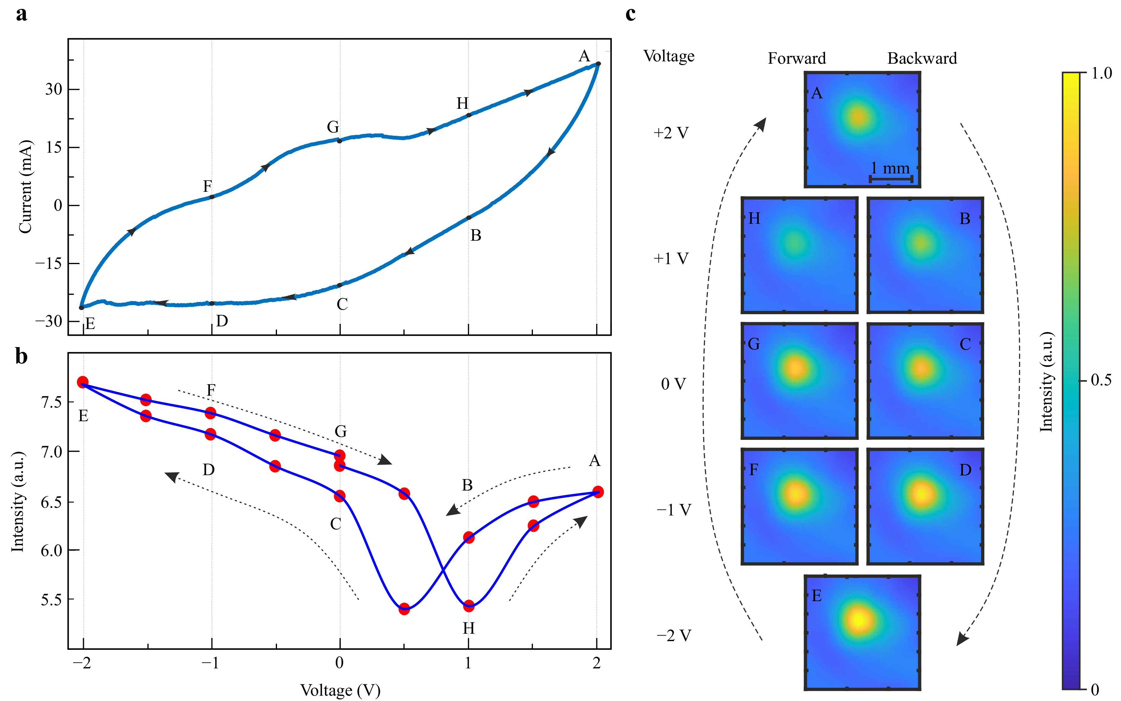
Fig. 4 Focusing performance of the fabricated FZP. a Cyclic voltammetry of the FZP. b Change in the focal spot intensity of the lens, based on FZP (red dots) for the voltage bias in the range of −2 to 2 V with the step of 0.5 V. The solid blue line is provided for clarity. c The intensity images at the focus position with blue and yellow representing the low and high intensity respectively. The intensity at −2 V is normalised to 1.0. The intensity takes the minimum values at +1 and the maximum at −2 V.
We demonstrated the active manipulation of the light intensity in the focus position of SWCNT FZP. Fig. 5a shows the lateral intensity profiles at the four bias voltages. The slightly asymmetric shape of the cross-section may be a sign of imperfections during fabrication. Despite the intensity modulation, FWHM was found to be almost independent of the applied voltage. Meanwhile, a negative voltage tended to narrow the Rayleigh range slightly, whereas a positive voltage produced the opposite effect (Fig. S3). FZP showed highly stable wavelength-scale (1.14$ \lambda $) focusing resolution. A reproducible switching behaviour was observed when impulse voltages of +0.5 and +1.5 V were applied. The average response time of the device, both during the rise and fall, consistently stood at 3.6 s (Fig. 5c), obtained as the lifetime of the single-exponential fit. The modulation speed, calculated as the switching frequency $ MS=1/\tau $ for our device, was 0.28 Hz. This slow response is attributed to complex ion transport-limited formation processes, which can be mitigated by adopting solid-state gating techniques. Moreover, a continuous random ramp-up and ramp-down of the voltage in 2.5-minute increments was conducted (Fig. 5d, approximately 13 min), demonstrating its stability over prolonged voltage cycling (Fig. 5d).
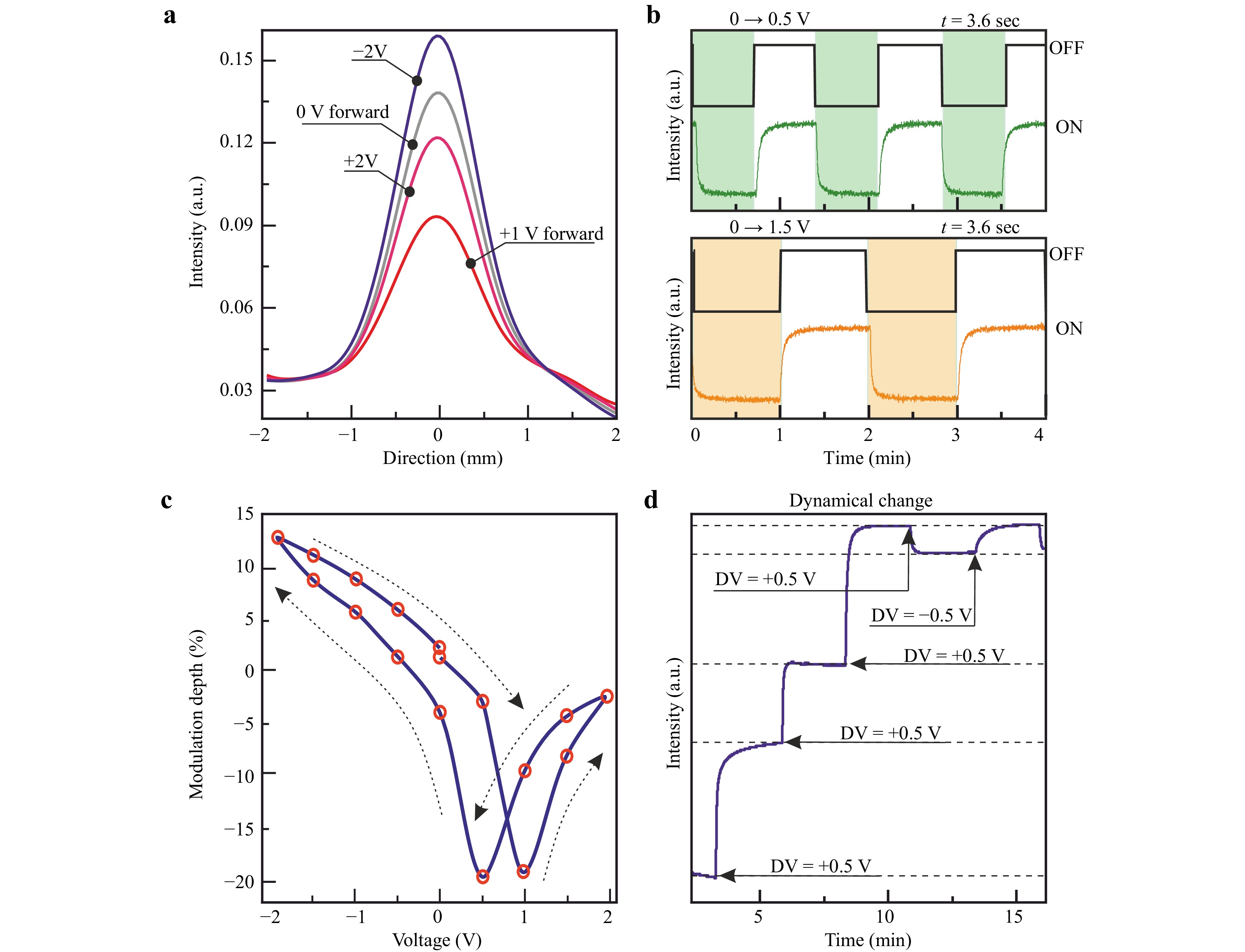
Fig. 5 Gate-tunable properties of the device. a Measured lateral intensity distributions at 0, +1, +2 and −2 V. b Time traces of the intensity at 0 to +0.5 V and 0 to +1.5 V sweep, every 40 and 60 seconds. c Calculated modulation depth of the FZP. d The dynamical time traces with continuous change with 0.5 V.
-
The proposed lens concept, which utilises ionic-liquid-gated FZP based on thin SWCNT films, presents a novel and valuable solution for highly efficient and integrable adaptive THz optics. Leveraging computational control for adaptive optics can lead to real-time optimisation of lens parameters based on environmental conditions and imaging requirements. It can facilitate autonomous focus and intensity adjustments and improve performance in dynamic settings. This advancement has opened a plethora of applications, including computational imaging and sensing. The benefits that can be obtained using intensity-tunable FZPs can be enhanced by the focus-tunable approach, which was introduced in our earlier work on stretchable devices22. The possibility of joint control of the real and imaginary parts of the reflective refractive index of SWCNT through electrochemical gating, as revealed in this study, allows the simultaneous modulation of the amplitude and phase of the passing THz wave, opening wide possibilities for the development of dynamic spatial modulators to obtain a variety of target complex wavefronts37. Possible tasks include controlled focusing, aberration correction38, pattern formation for THz single-pixels39, and ghost imaging40. Thus, this study can significantly increase the adaptability of optical systems for various applications in the THz range. Furthermore, the implementation of advanced gating schemes featuring local and interleaved gating electrodes may significantly expand the range of tunable functionalities. In addition, the possibility of FZP ring adjustment holds great promise for the development of multi-focus lenses that are in high demand for super-resolution imaging.
A comparison of the present work on the dynamic control of THz waves with published studies highlights their distinctive advantages in terms of performance and practical viability. In particular, our device offers a balance between modulation depth (35%), fabrication simplicity, scalability, and additional focusing functionality. Although graphene-based modulators achieve faster switching (e.g. 0.1 ms), they require complex cleanroom-based fabrication processes41. In Refs. 42, 43 turn-on delays below 1 ms were reported in metamaterial-based systems, but still lacked scalability owing to the complex fabrication. In contrast, our method demonstrates enhanced large-scale fabrication potential through cost-effective processes that are suitable for industrial applications. Furthermore, compared with Ref. 44 and Ref. 18, who focused on high-resolution near-field THz imaging with a limited dynamic range, our device provides a remarkable attenuation efficiency of 8 × 10⁸ dB cm2 g−1, enabling more robust non-destructive imaging.
A promising direction for improving a single device is to increase the thickness of the CNT film. Additionally, it is possible to deposit two FZPs on separate quartz substrates facing each other in a sandwich-like structure with an ionic liquid as the separator. This structure doubled the modulation depth, similar to that of a graphene modulator17.
Unlike conventional lithography-based metamaterials, our CNT-based approach offers significant advantages in terms of scalability and cost-effectiveness. CNT films produced using the aerosol (floating catalyst) chemical vapour deposition method potentially enable high-throughput production at substantially lower costs than traditional cleanroom fabrication processes. The inherent stretchability of our CNT films provides an additional degree of freedom for device functionality, allowing the mechanical tuning of the focus point, as demonstrated in22. This mechanical tunability combined with electrical modulation via ionic-liquid gating, offers a unique hybrid control mechanism that is not readily available for conventional rigid metamaterial structures. Although we achieved modulation depths comparable to other metamaterial approaches, our device architecture maintained its performance across a broader frequency range because it did not rely on resonant structures with inherently narrow-band responses.
The proposed THz system with dynamic modulation capabilities represents a significant advancement in precision imaging and biological applications. The incorporated dynamic modulators demonstrate superior resolution and an enhanced signal-to-noise ratio compared to conventional static modulation approaches, while maintaining a high temporal resolution in the dynamic operation mode45. These performance characteristics make the system particularly valuable for applications requiring the precise spatiotemporal control of THz radiation. Extensive experimental studies have established the profound effects of terahertz radiation on cellular processes, particularly on the regulation of genes associated with stress responses, inflammation, cell cycle control, and programmed cell death and growth46, 47. Notably, a significant modulation was observed in the expression profiles of heat shock proteins, inflammatory cytokines, and growth factors under controlled terahertz exposure. However, achieving reproducible biological effects requires addressing several technical and methodological challenges primarily related to the precise control of exposure parameters. To overcome these limitations, we designed and implemented an advanced optical setup featuring dual electrochemical modulation elements: a gated lens positioned before the photonic crystal waveguide, and a stabiliser cell positioned after it (Fig. 6a). A photonic crystal waveguide, previously optimised for targeted THz radiation delivery48, works in concert with these elements to enable precise control over both the spatial distribution and intensity of THz radiation. By independently adjusting the voltages applied across the lens and stabiliser contacts, we achieved accurate control over the THz beam parameters (Fig. 6b), enabling future systematic investigation of dose-dependent biological responses. Intensity mapping demonstrates the sophisticated interplay between two independent control parameters: the voltage applied to the adjustable lens and that applied to the stabiliser. In addition, the SWCNT-based tunable FZP demonstrated in this study holds significant promise for advanced photonic applications, particularly in self-homodyning detection and laser feedback interferometry, provided that the response time is improved49.
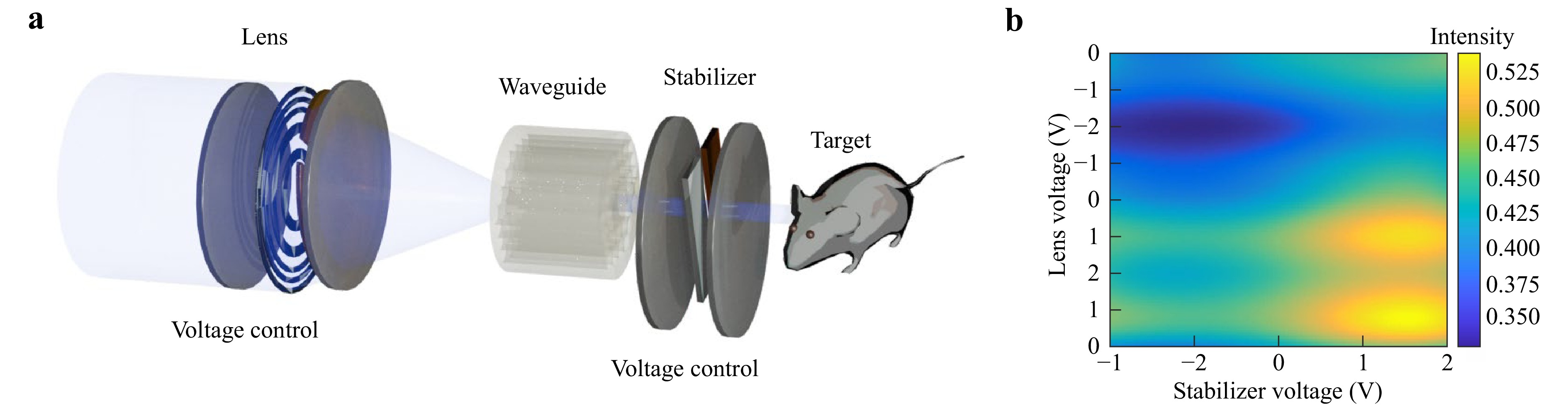
Fig. 6 a The schematic illustrates a dual-modulation architecture for precise THz radiation delivery. The system integrates two key control elements: an adjustable FZP preceding a photonic crystal waveguide, and an electrochemical cell (stabiliser) positioned after it in front of envisioned target. This sequential arrangement enables dynamic control over the beam's intensity under lens and cell voltage control through the waveguide structure, as depicted in b.
-
In summary, we developed an intensity-tunable planar ultra-thin lens device in which the focus intensity can be electrically controlled via electrochemical gating. It was possible due to the unique optical properties of SWCNT thin films exhibiting pronounced gate-tunable intraband absorption in the THz frequency range. In particular, it was achieved due to remarkable shielding effectiveness, reaching up to 8 × 10⁸ dB cm2 g−1 at low density (2.4 mg/cm3) and thickness (40 nm). Using this feature, we achieved a variation in the modulation depth from −20 to +15%. Simultaneously, the device maintained the same focal position (Fig. S7), and FWHM did not vary significantly for all the applied biases. Overall, the results demonstrate the role of electrochemical doping in the operation of thin optical elements, providing a promising area for future implementation in THz systems.
-
Patterned thin films of single-walled carbon nanotubes for FZP were fabricated using the aerosol (floating catalyst) chemical vapour deposition method21, which is based on CO decomposition through the Boudouard reaction occurring on the surface of Fe-based catalyst aerosol particles. The SEM image of the pristine SWCNT film shows the morphology of the randomly oriented SWCNTs composed of the FZP (Fig. S6). The patterning procedure described here employs SWCNT films as opaque regions of the FZP, as developed elsewhere22, 23. Initially, a custom pattern for the FZP was etched into a stainless-steel plate using pulsed laser ablation, resulting in a rigid stencil with a height difference of 150–200 $ \mathrm{\mu} $m. Subsequently, the pattern was imprinted onto a nitrocellulose filter (HAWP, Merck Millipore, with a pore size of 0.45 $ \mathrm{\mu} $m) by passing the filter affixed to the metal stencil through rollers to compress specific pore areas, thereby reducing throughput. The areas of the stencil containing the engravings left the nitrocellulose filter unaffected. Subsequently, the SWCNT aerosol was deposited onto the uncompressed areas of a nitrocellulose filter to create a thin nanotube film that mirrored the geometry of the metal stencil. Finally, the resulting film was dry-transferred onto a quartz substrate24) onto a quartz substrate (Fig. S4). The ionic liquid, BMIM NTf2, was produced using a standard procedure described elsewhere50. Briefly, the alkylation of 1-methylimidazole by 1-bromobutane was followed by anion exchange with lithium bistriflimide in water. The choice of BMIM NTf2 as the ionic liquid is crucial for several reasons, as demonstrated in our control experiment comparing the CNT–FZP device performance with and without an ionic-liquid layer22. While the cell showed superior focusing performance even without an ionic liquid, achieving efficient carrier density modulation under a low-voltage bias would be significantly challenging without it. The electrochemical stability window of BMIM NTf2 is particularly wide ([−2, +2]V), which is crucial for reliable operation without degradation under an applied voltage bias51, and its stability in air is another critical practical advantage not found in many other ionic liquids52. BMIM NTf2's optical properties are particularly suitable for this application because of its transparency across broad THz ranges and stability under an applied voltage (Fig. S1), which is essential for maintaining high transmission efficiency while enabling the desired electrochemical effects, with such transparency being rare among other ionic liquids and critical for device operation. The average response time of the device, both during rise and fall, is obtained as the characteristic time constant $ \tau $ of a single-exponential fit in the form of $ I=I_{0}+Ae^{-t/\tau} $ where I$ _0 $ is the baseline current and $ A $ is the amplitude of the exponential component.
-
Raman mapping was performed using a confocal scanning Raman microscope (Horiba LabRAM HR Evolution, HORIBA Ltd., Kyoto, Japan) with a 532 nm laser wavelength (with a spectral resolution of 0.5 cm−1). Measurements were carried out using linearly polarised excitation at wavelengths of 532 nm, an 1800 lines/mm diffraction grating, and ×10 objective. The spot size is approximately 0.4 $ \mathrm{\mu} $m. The samples were mounted on motorised stages which allowed for a 2D x–y scan.
We employed a custom-built (GPI RAS) transmission-mode terahertz (THz) pulsed spectrometer for THz spectroscopy. This system utilises a pair of photoconductive antennas for emission and detection of THz pulses. To mitigate the effects of water vapour in the laboratory environment, the THz beam path was maintained under vacuum at approximately 10−3 mbar. The spectrometer operates within a spectral range of 0.05–2.5 THz and achieves a spectral resolution of up to 0.015 THz.
-
Experimental verification of the produced THz lens was performed using an in-house THz continuous-wave imaging setup. As a source of linearly polarised THz radiation, we used a BWO (GIP RAS) operating at a frequency of 327 GHz with a beam spot size as shown in Fig. 1c. The detector (Golay cell) was mounted on motorised linear translation stages, which enabled a 3D pixel-by-pixel scan of the THz field intensity53. For THz imaging experiments, a solid immersion lens was integrated into the system. In a THz imaging experiment, a solid immersion lens was integrated into the system14, 54. The device showed an exponential change in transmission that stabilised and came to a plateau within several minutes. It is important to note that after several minutes of waiting, the cell was run for several hours until the x-y and x-z scans were completed. The reproducibility test states that the intensity values are the same for complete x-y and x-z scans taken at the same voltage during 2nd and subsequent cycles.
-
For numerical simulation of the Field interaction with the FZP, COMSOL Multiphysics Software was applied. The quasi-3D finite-element frequency-domain (FEFD) method was used for modelling the optical element with rotational symmetry with respect to the optical axis. The simulation volume was restricted using perfectly matched layers as absorbing boundaries. In the simulation, we implemented an infinitely thin 2D object with varying surface conductivity as a zone-plate material.
-
The authors would like to acknowledge the Clover Initiative. AVR, MGB, and AVA would like to acknowledge the Ministry of Science and Higher Education (FSMG-2025-0005, Imaging Experiments). AVR, MIP, and MGB acknowledge the Russian Science Foundation grant (Project No. 24-79-00143; Spectroscopy Measurements). GMK acknowledges a Russian Science Foundation grant (project No 25–79–10280; THz waveguiding delivery experiment). NIR, AAM, YGG, and AGN acknowledge the Russian Science Foundation grant (project No. 22-13-00436; Synthesis of SWCNTs).
Gate-tunable fresnel zone plate based on single-walled carbon nanotubes for terahertz applications
- Light: Advanced Manufacturing , Article number: 4 (2026)
- Received: 25 August 2025
- Revised: 14 November 2025
- Accepted: 28 November 2025 Published online: 19 March 2026
doi: https://doi.org/10.37188/lam.2026.004
Abstract: The active manipulation of electromagnetic waves through electrical tuning of nanomaterials is a key advantage for modern technology. We employed the tunable optical response of ionic-liquid-gated single-walled carbon nanotube (SWCNT) films to address a major challenge in terahertz (THz) optics – the limited range of materials with suitable optical properties. In this study, we demonstrated a high-performance THz intensity modulator combined with a focusing Fresnel zone plate (FZP) integrated in electro-chemical cell. We introduce a new approach for designing and fabricating the FZP, based on pre-measured dielectric properties of SWCNT films under applied voltage. The superior shielding effectiveness (up to 8 × 10⁸ dB cm2 g−1) of SWCNT films enables the creation of an ultrathin terahertz lens. Electrical gating doubled the minimum refractive index, enhancing lens performance. This also enabled in situ tunability of the intensity modulation depth, from +15 to –20%, with an applied voltage of +2 to –2 V. Although the current switching time is 3.6 seconds, our work presents the first demonstration of an electrochemically gated SWCNT FZP, offering distinct advantages in tunability and thin-film design. Operating at 327 GHz, this FZP is a promising solution for novel adaptive THz communication devices.
Research Summary
Unique Tunable THz Lens from 6G Communications to Biological Sensing
For the first time scientists have developed a lens capable of tunable controlling the intensity of terahertz radiation. Such radiation holds a special place in the electromagnetic spectrum between electronics and photonics. Being the least studied ranges of the electromagnetic spectrum, it raises the main problem of the scientific community - the lack of the available terahertz optical elements. In classical setups, static lenses with fixed parameters are used. The main motivation for this work was the possibility of dynamic lens control, which will allow the creation of adaptive optics for medicine, 6G technology etc. It could adjust the power to study living tissue without causing damage. In communications, it could optimize signal strength for faster data transfer thus solving a key bottleneck, paving the way to move from the laboratory into real-world devices.
Rights and permissions
Open Access This article is licensed under a Creative Commons Attribution 4.0 International License, which permits use, sharing, adaptation, distribution and reproduction in any medium or format, as long as you give appropriate credit to the original author(s) and the source, provide a link to the Creative Commons license, and indicate if changes were made. The images or other third party material in this article are included in the article′s Creative Commons license, unless indicated otherwise in a credit line to the material. If material is not included in the article′s Creative Commons license and your intended use is not permitted by statutory regulation or exceeds the permitted use, you will need to obtain permission directly from the copyright holder. To view a copy of this license, visit http://creativecommons.org/licenses/by/4.0/.

 DownLoad: