


-
The advancement of additive manufacturing (AM) technologies has revolutionized the fabrication of complex three-dimensional structures, enabling innovations across various scientific and industrial domains. Glass, known for its exceptional hardness, optical transparency, chemical stability, and heat resistance, plays a pivotal role in applications such as optics, photonics, medical devices, and microfluidics1–3. In particular, its ability to precisely manipulate and transmit light with minimal distortion makes it indispensable for high-performance optical components like lenses, phase masks, and diffraction gratings, foundational elements in imaging, communication, and laser systems. Despite its potential, the inherent brittleness and hardness of glass pose significant challenges to conventional manufacturing methods. Traditional AM techniques struggle to achieve the precision, contour accuracy, and transparency required for optical applications4–6.
Furthermore, existing glass additive manufacturing methods, such as Selective Laser Sintering (SLS)7, fused deposition modeling (FDM)8, and direct ink writing (DIW)9, rely heavily on melting or sintering processes. These approaches often result in parts with poor dimensional accuracy, suboptimal surface quality, and opacity, rendering them unsuitable for optical applications10.
Laser-Induced Forward Transfer (LIFT) is an additive manufacturing technique that enables high-resolution printing of diverse materials under ambient conditions11. It involves depositing a thin donor film onto a transparent carrier substrate, from which precise portions of material are ejected by a pulsed laser and deposited onto a nearby receiver substrate. This approach has been widely applied to metals, ceramics, and polymers11–13, using both molten and, more recently, solid-state donor films14. Unlike melting-based transfer, which can compromise fine structural details, solid-state LIFT enables the preservation of microstructures, offering enhanced resolution and material integrity. However, the technique has not yet been thoroughly explored for glass-on-glass applications, where challenges such as poor adhesion, fragmentation, disintegration, and unintended material mixing persist15.
To overcome these issues, methods like Dynamic Release Layer (DRL)-LIFT16 and Blister Actuated LIFT (BA-LIFT)17 or Blister-Based LIFT (BB-LIFT)18 have been developed. DRL-LIFT uses a thin dynamic release layer that absorbs laser energy, decomposing or evaporating to create localized pressure that propels the donor material to the receiver substrate. BB-LIFT employs a thicker blister layer, typically metals or polymers, which thermally expands upon laser absorption, forming a blister to drive the material with minimal laser impact. However, these methods have notable drawbacks. DRL-LIFT can leave release layer residues, contaminating the transferred material, while BB-LIFT requires complex substrate preparation, including blister layer fabrication and coatings, increasing cost and complexity. Furthermore, blister formation dynamics can vary, affecting repeatability and limiting suitability for some applications16–19.
Pulsed lasers enable precise material processing at micro and submicron scales. However, in the case of glass, the challenges of weak light absorption and brittle mechanical behavior often limit the effectiveness of such methods. Previous work from our group has explored the laser processing capabilities of silicon suboxide (SiOx, x < 2) films. This glassy material, while transparent in the green to infrared spectrum, exhibits strong absorption in the blue-UV range, making it well-suited for UV laser processing. SiOx can also be oxidized to SiO2 with an accompanying volume increase, all while maintaining contour accuracy20–22. We have demonstrated the feasibility of transferring SiOx films using the Laser-Induced Forward Transfer (LIFT) technique, achieving solid-state transfer with minimal surface melting. This process enabled the precise formation of well-defined printed pads and strips with high surface quality. Although successful transfers of SiOx films onto polymeric substrates such as PDMS and polycarbonate demonstrated excellent precision, quality, and adhesion, challenges remain. Specifically, the oxidation of SiOx to SiO2 requires heating to temperatures up to 1000°C, making the process incompatible with polymer substrates. Moreover, attempts to transfer SiOx films onto glass substrates failed due to fragmentation and poor adhesion, preventing their effective use in fabricating optical elements or achieving SiO2 conversion on glass23.
Previous studies on solid-state material transfer have demonstrated that minimizing the gap between the donor and receiver substrates significantly improves the quality and fidelity of the transferred material18,24. Reducing this distance to near-zero enhances the precision of the transfer, resulting in patterns on the receiver substrate that more closely match the shape of the laser spot. However, achieving a truly zero-gap interface is inherently challenging due to imperfect flatness of the substrates. Even when the donor and receiver are brought into contact, this imperfection often leaves a residual gap of several micrometers. Such gaps can result in defects during the transfer, including incomplete material deposition, structural breaks, or weak adhesion.
Our research focuses on advancing the application of LIFT for printing solid glass directly onto a solid substrate. The donor material, substoichiometric silicon oxide (SiOx, where x < 2), was efficiently deposited as thin films on transparent fused silica substrates using physical vapor deposition (PVD), following the method previously reported by our group25. Since this material exhibits sufficient UV absorption to facilitate the LIFT process, we used a UV excimer laser for this purpose. Achieving precise material transfer required maintaining close contact between the donor and receiver substrates, as well as carefully matching the laser fluence to the thickness and absorption coefficient of the donor material. To enhance the fidelity of material transfer, we designed a custom system to minimize the gap between donor and receiver substrates. This system ensured near-contact interfaces through controlled pressure distribution, achieving submicron gaps. Additionally, the matching of laser fluence with the thickness of the donor material was systematically investigated, significantly improving transfer quality.
The ability to directly print solid-state SiOₓ structures onto optical glass substrates enables the fabrication of compact, robust, and UV-compatible optical elements without relying on photolithographic processing. One key application is the fabrication of binary phase masks (BPMs), which benefit from the excellent surface quality, precise contour definition, and mechanical stability provided by this technique. These BPMs can be employed for wavefront shaping, beam splitting, and optical filtering in laser systems and interferometric setups, where accurate phase modulation and high optical quality are essential26. In addition to BPMs, the patterned layers are also promising for the fabrication of advanced diffractive optical elements such as axicons, computer-generated holograms, and microlens arrays27, components that are increasingly utilized in laser micromachining28 and structured illumination microscopy29.
This work introduces a solid-state LIFT strategy that enables the direct transfer of substoichiometric SiOₓ thin films onto transparent glass substrates with submicron fidelity, without requiring intermediate absorbing layers. In contrast to DRL-based or blister-based LIFT techniques, our method avoids contamination, reduces process complexity, and enables reproducible transfer without thermal decomposition or blister formation. Moreover, compared to conventional lithography-based fabrication, this process is maskless, solvent-free, and etch-free, allowing direct patterning on curved or UV-transparent substrates. Additionally, the transferred SiOₓ films can be thermally oxidized into SiO2, enabling the fabrication of UV-grade components for optical applications in the deep-UV spectral range. These features establish our method as a robust and scalable alternative for high-resolution glass-based micro-optical fabrication.
-
For the donor substrate, SiOx films (where x < 2) with thicknesses ranging from 180 nm to 1000 nm were deposited onto 2 mm thick fused silica substrates serving as the carrier, using physical vapor deposition (PVD). The deposition process involved the thermal evaporation of SiO pellets (3–6 mm in size, 99.99% purity) within a baffled box housed in a Univex 350 chamber. The evaporation rate was precisely controlled at 1 nm/s under a vacuum pressure of approximately 3 × 10⁻⁶ mbar. To improve layer adhesion, the substrates were heated to 300 °C throughout the process and subjected to surface sputtering with argon ions for 30 seconds prior to the evaporation. These films are denoted as SiOx to reflect their indeterminate oxidation state, as the oxygen content depends on the residual oxygen pressure in the chamber during deposition, leading to x < 2. The average stoichiometry of SiOₓ films deposited under comparable PVD conditions was previously determined by STEM-EDX to be SiO1.08 ± 0.0230. These coatings exhibit notable characteristics, including high hardness, excellent adhesion, and high transmission in the visible spectral range and at the same time significant ultraviolet absorption, with an absorption coefficient of approximately 2.7 × 104 cm−1 at 248 nm31. Bare SiO2 (fused silica) and BK7 (borosilicate) glass substrates were utilized as receiver substrates.
-
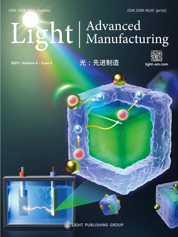
A custom mechanical system was specifically designed for this study to ensure precise alignment and minimal spacing between the donor and receiver substrates (Fig. 1a-d). The system consists of two dedicated holders, each equipped with spring-loaded clamping rings to maintain controlled contact pressure. The receiver holder includes a central and peripheral spring configuration, allowing uniform force distribution across the substrate. An adjuster plate and linear translation unit enabled fine positional control along the x-axis, establishing near-contact conditions essential for clean material transfer.
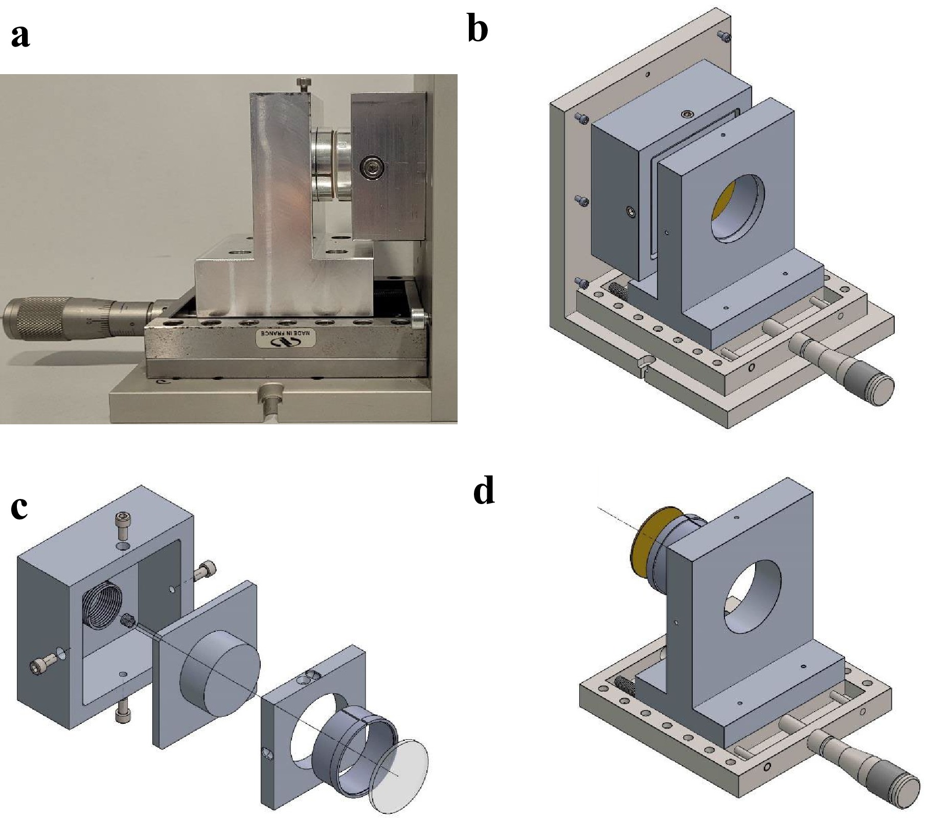
Fig. 1 Mechanical setup for precise alignment of the donor and receiver substrates. a Real image, b Schematic diagram. c receiver holder, d donor holder.
The entire setup was mounted on a computer-controlled three-axis stage, allowing precise adjustments. This mechanical design minimized the air gap between the substrates to submicron levels and reduced unwanted deformation or misalignment, which is a critical condition for the homogeneous transfer of the silicon suboxide layer onto the receiver substrate.
To evaluate the pressure distribution at the interface, Fujifilm Prescale pressure-sensitive films were used. These films consist of two layers, a microcapsule-coated color-forming sheet and a color-developing layer. When pressure is applied, the capsules rupture, creating a visible red coloration whose intensity corresponds to the local pressure. Two film types (4LW and LLLW), covering the 0.05–0.60 MPa range, were used to confirm that compression provided a uniform pressure distribution across the substrates.
-
The optical configuration used to direct the laser beam onto the sample surface is illustrated in Fig. 2. The samples were irradiated using a KrF excimer laser (248 nm, 25 ns pulse duration; Lambda Physik LPX 200). A variable slit was used to shape the beam, which was then projected onto the donor film with 10:1 demagnification using a spherical lens (f = 100 mm). To achieve optimal conditions for printing of SiOₓ on receiver substrates, the laser fluence was systematically adjusted using a variable attenuator. The sample was exposed to single-pulse irradiation from the rear side of the donor substrate.
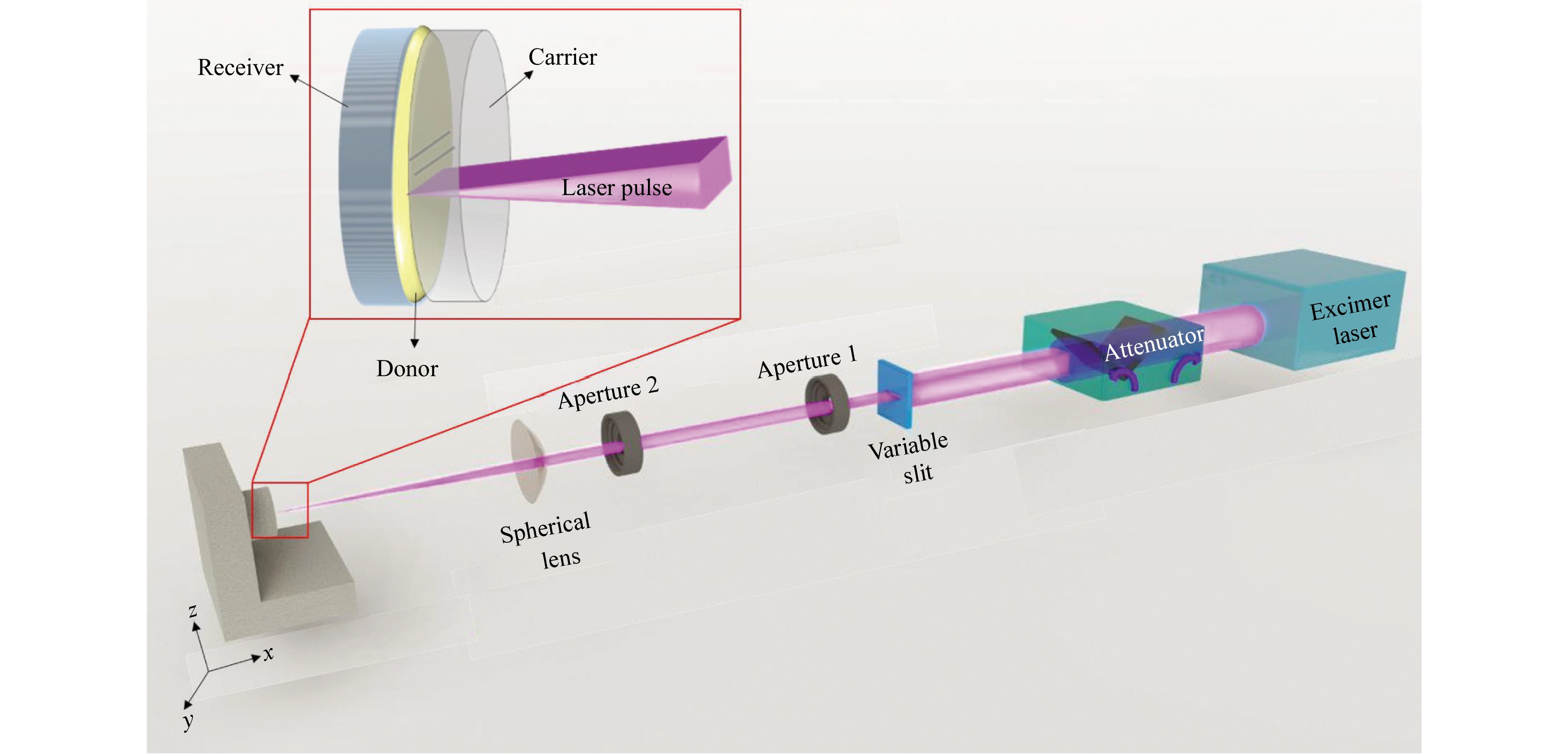
Fig. 2 Diagram of the optical configuration used to direct the laser onto the sample surface.
Line structures were printed by projecting the slit-shaped beam onto the donor film and translating the sample using a computer-controlled three-axis stage. The length of the printed lines was adjusted by partial beam blocking with apertures placed near the slit and the lens. The steps involved in printing strip structures onto the receiver substrates are illustrated in Fig. 3.
Fig. 3 Schematic of the process steps involved in printing of strip patterns on the receiver substrates.
In case of a desired UV-transparency, the receiver fused silica was treated subsequently by thermal annealing at a temperature of 1000 ℃ for 48 hours in an air atmosphere.
-
A binary phase mask was subsequently fabricated using the described additive manufacturing method. For this application, as previously mentioned, slit projection was employed to generate a laser pulse with a line-shaped spatial beam profile, enabling the desired phase grating pattern to be constructed incrementally, line by line. A grating with a duty cycle of 0.5 (i.e., equal width of lines and spaces) was thus fabricated. Following the fabrication, we investigated the diffractive pattern of the phase mask using a HeNe laser beam with a wavelength of 632.5 nm. The diffraction efficiencies were then measured using a beam diagnostic system.
-
The printed components, both before and after thermal annealing, were analyzed using various characterization techniques, including Scanning Electron Microscopy (SEM, ZEISS EVO MA10) and Optical Microscopy (OM, ZEISS Axio Imager.Z2m). Surface topography measurements were performed using a surface stylus profilometer (Bruker DektakXT). Additionally, the thickness of the deposited layer and the air gap between the receiver and donor were determined using a Filmetrics F20-UV optical thickness measurement system equipped with an LS-DT2 light source.
-
To evaluate the mechanical stability of the printed SiOₓ structures and to assess practical cleaning approaches, three procedures were applied to the fabricated binary phase masks:
(1) Blow-off with dry nitrogen gas (~2 bar).
(2) Drag wiping using cleanroom-grade wipes wetted with acetone.
(3) Immersion in acetone for 2 minutes followed by drying with a nitrogen stream.
Optical microscopy was performed before and after each cleaning step to monitor surface condition and structural integrity.
-
As mentioned earlier, in solid-state material transfer, the quality and fidelity of the transferred material strongly depend on the gap between the donor and receiver substrates. To minimize this gap, a custom-designed compression system was used, as illustrated in Fig. 1. The effect of substrate distance on the quality of printed stripes was analyzed under two different conditions: (1) simple contact between the donor and receiver substrates and (2) additional applied force to further reduce the air gap.
Fig. 4a presents an SEM image of the printed SiOx strip (thickness: 700 nm) on a fused silica substrate under the first condition, where the substrates were merely in contact. The printed strip shows significant fractures and fragmentation, indicating an unsuccessful transfer of the SiOx layer. In contrast, Fig. 4b demonstrates that applying maximum compression results in a uniform and smooth printed strip with well-defined contours, ensuring a successful transfer.
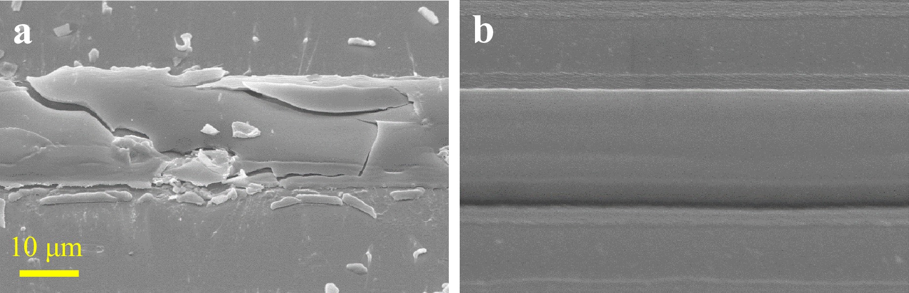
Fig. 4 SEM images of SiOx strips (705 nm) printed on fused silica using a fluence of 1.25 J cm−2. a Without external compression b With applied compression.
To quantify the air gap under both conditions, Filmetrics optical thickness measurements were conducted (Fig. 5a, b). In the simple contact condition, the air gap exceeded 8 μm. However, under maximum compression, the gap was reduced nearly tenfold to below one micron.
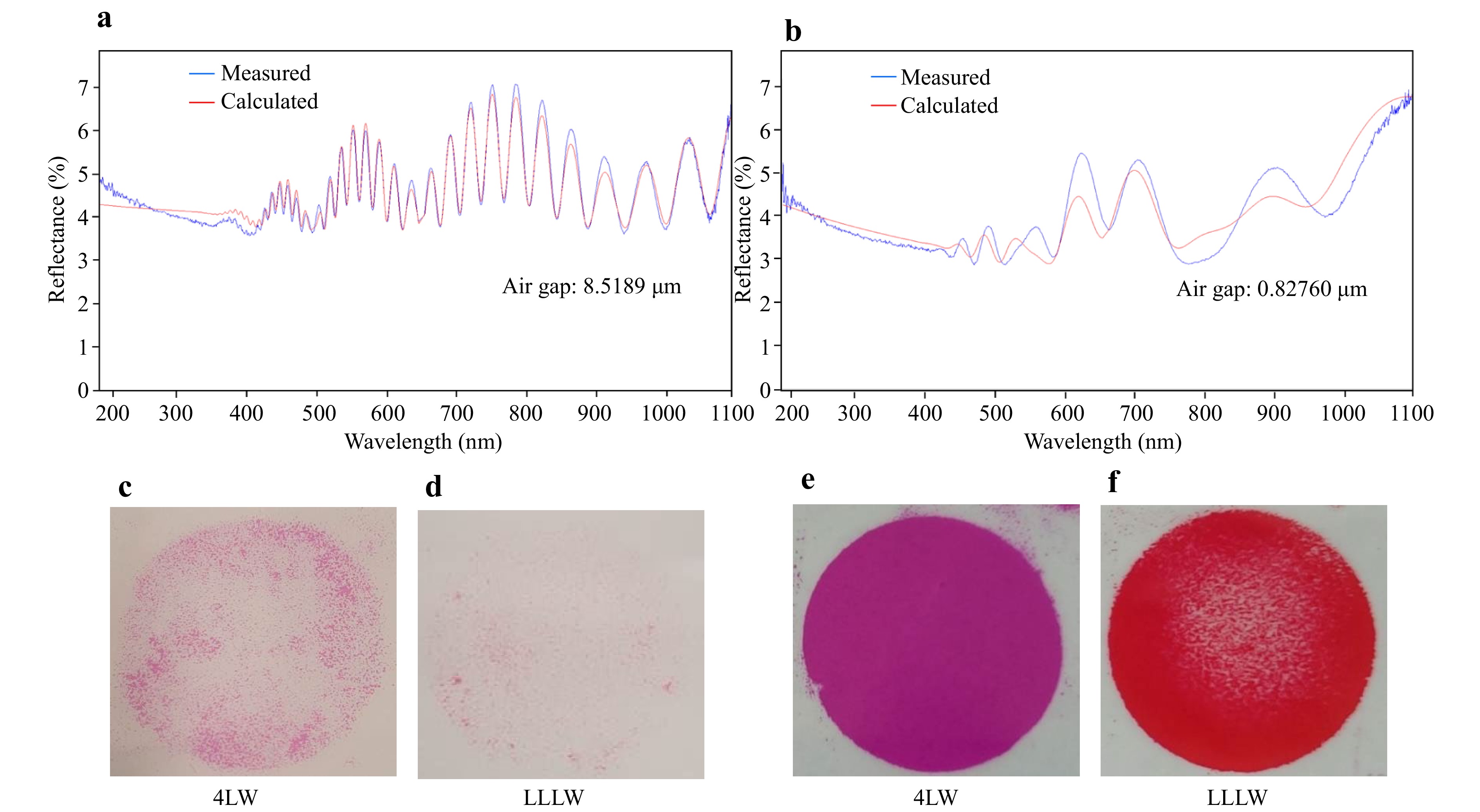
Fig. 5 a, b Reflectance spectra used to estimate the air gap between donor and receiver substrates: a simple contact; b compressed contact. c-f Pressure distribution visualized using Prescale films: c, d simple contact; e, f compressed contact.
Furthermore, the pressure distribution on the substrate surfaces was analyzed using Prescale film under both conditions. Given that the springs in the mechanical setup exert a maximum pressure of 54 N cm−2 (0.54 MPa), 4LW and LLLW Prescale films, sensitive to pressure ranges of 0.05–0.20 MPa and 0.20–0.60 MPa, respectively, were used to visualize the distribution. As shown in Fig. 5c, d, in the simple contact condition, the pressure distribution was minimal and inhomogeneous. However, under maximum compression (Fig. 5e, f), the substrates experienced a nearly uniform pressure ranging from 0.20 to 0.54 MPa.
Clearly, the significant reduction in distance plays a crucial role in successfully transferring the SiOx layer onto the glass substrate. The gap between the donor and receiver substrates greatly influences stress distribution, energy dissipation, film adhesion, and the structural integrity of the printed layer.
When the substrates are separated by more than a few microns, the transferred material becomes highly susceptible to fragmentation and mechanical failure, as observed in Fig. 4a. This fragmentation can be attributed to shock wave interference, inhomogeneous pressure distribution, and insufficient adhesive interaction between the SiOx layer and the fused silica substrate. Reducing the gap below one micron, as achieved through the custom-designed compression system, significantly enhances the cohesion and adhesion mechanisms during transfer. In a closely spaced configuration, air resistance and energy dissipation effects in the transfer pathway are minimized, allowing the material to reach the receiver substrate before significant thermal or mechanical relaxation occurs. This helps maintain the integrity of the donor layer and its adhesion to the receiver surface. Moreover, shock waves generated by laser pulses can disrupt material deposition when the gap is too large32–34. By decreasing the separation, the influence of these shock waves is lessened, reducing secondary reflections that could otherwise disturb the material deposition process. Additionally, pressure distribution analysis using Prescale films (Fig. 5c-f) confirms that reducing the gap results in a more uniform pressure distribution, ensuring a homogeneous transfer of the SiOx layer while preventing stress-induced fractures.
-
To evaluate the efficiency and versatility of the proposed additive manufacturing process, SiOx strips with varying thicknesses, ranging from approximately 180 nm to 1000 nm, were printed onto different glass substrates, including fused silica and BK7. The objective was to achieve the highest possible quality of the printed strips. Laser fluence, a critical parameter in laser-induced forward transfer (LIFT), governs both the initiation of material detachment and the quality of transfer onto the receiver. Previous studies18,34 have demonstrated that laser fluence plays a crucial role in material transfer processes and must be optimized for each specific material and thickness.
In this study, we distinguish between two key fluence values: the threshold fluence (Fth), defined as the minimum fluence required for the detachment of the SiOx film from the donor substrate; and the optimum fluence (Fopt), which ensures not only complete detachment but also intact and stable adhesion of the transferred film to the receiver substrate without structural degradation.
In Fig. 6a, Fth and Fopt are presented as a function of the SiOₓ film thickness, based on four discrete thicknesses investigated experimentally. Intermediate thicknesses were not available due to deposition constraints; however, for each selected thickness, multiple (3–5) repeated measurements were conducted to ensure reproducibility and statistical confidence. The connecting lines between data points are provided as visual aids to highlight the observed monotonic trend and are not intended as fitted interpolations. Furthermore, the color-coded regions in the diagram qualitatively represent different transfer regimes, derived from experimental observations. Representative SEM images corresponding to each regime for the 950 nm thickness are included in Fig. 6b-d to support the physical classification. As expected, both Fth and Fopt exhibit a nearly monotonic increase with film thickness.
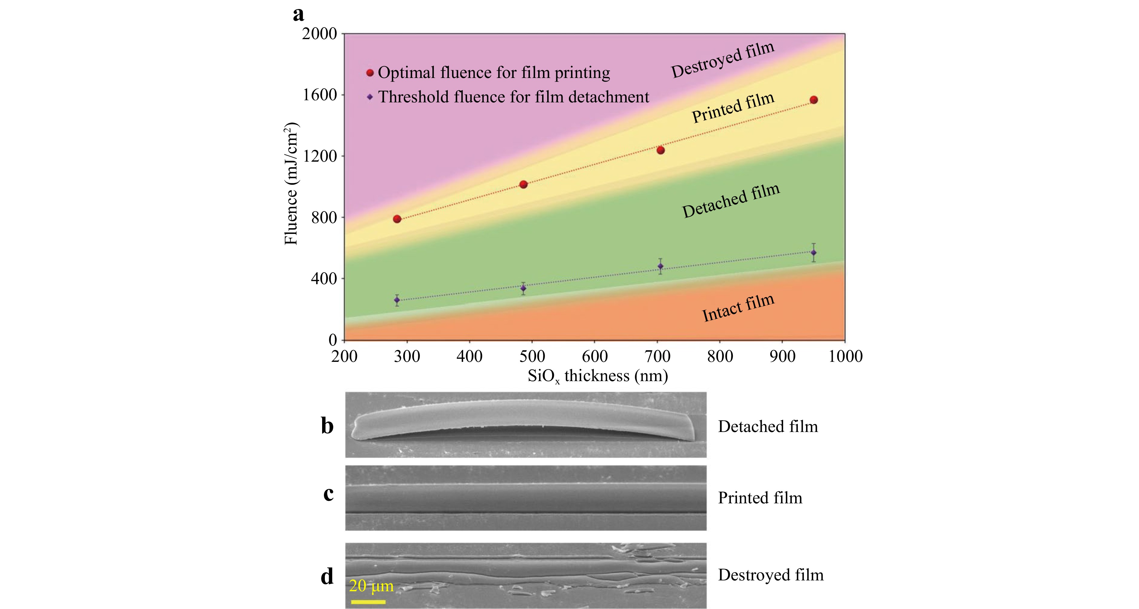
Fig. 6 a Threshold (Fth) and optimum (Fopt) fluences versus SiOₓ film thickness, based on four experimentally studied values. Each point represents the average of 3–5 measurements. Color-coded regions indicate transfer regimes identified from experiments. b-d SEM images (taken at a 60° tilt angle) of the 950 nm film thickness for different regimes: b detachment without adhesion, c successfully printed, and d destroyed structures.
This correlation arises from several interrelated physical factors. The force required to tear the film away from the surrounding, still adhering film scales linearly with the film thickness, assuming either tensile or shear loading. This leads to the requirement for a greater mechanical impulse to initiate separation. As a result, the threshold fluence must be increased to generate sufficient stress at the donor–carrier interface.
In addition, thicker layers lead to greater thermal dissipation within the donor film, limiting the amount of energy that can propagate toward the upper regions of the material. This reduction in laser energy efficiency negatively affects the quality of the transfer, as the decreased energy and corresponding surface temperature may fall below the level required for sufficient adhesion of the donor film to the receiver substrate.
Thus, while Fth is primarily influenced by the cohesive strength and internal film bonding, Fopt is governed by a more complex interplay of the aforementioned factors.
As illustrated in Fig. 6, for a given thickness, fluences below Fth result in no visible detachment the film remains entirely on the donor. In the intermediate regime between Fth and Fopt, detachment may occur, and in some cases, the film may even reach the receiver substrate but fails to adhere. Only within a narrow fluence window near Fopt is defect-free and stable printing achieved. Beyond Fopt, excessive laser energy leads to destructive effects such as donor film rupture and ablative debris, compromising structural fidelity. The increasing absorption with film thickness is also confirmed by transmission measurements shown in Fig. S1.
In addition to experimental observations, numerical simulations were conducted to further clarify the influence of film thickness on thermal behavior during laser irradiation. In these simulations, the donor–substrate interface was not treated as a distinct boundary. Instead, the donor and substrate were assumed to share identical thermal properties, effectively eliminating the need to model interfacial heat transfer. This approximation is justified by the simplified nature of the simulation, which aims to qualitatively reveal how variations in film thickness affect thermal penetration and back-side heating. In this framework, the one-dimensional heat conduction equation,
$$ \rho c\frac{\partial T}{\partial t}=\kappa \frac{{\partial }^{2}T}{{\partial z}^{2}}+\alpha I\left(z,t\right) $$ was solved, where $ T\left(z,t\right) $ is the local temperature as a function of spatial coordinate z and time t, $ \rho $ is the density, c is the specific heat capacity, and $ \kappa $ is the thermal conductivity of the material. For SiOx, material properties (except absorption coefficient) similar to those of SiO2 were assumed, based on reported similarities35. The laser source term $ I\left(z,t\right) $ was modeled using the Lambert-Beer law:
$$ I\left(z,t\right)={I}_{0}\left(t\right)\left(1-R\right){e}^{-\alpha z} $$ where $ \alpha $ is the absorption coefficient and R the reflectance. The absorption coefficient used in the simulation (2.7 × 104 cm−1 at 248 nm) corresponds to the value reported for thermally evaporated SiOₓ films prepared under similar conditions31. A Gaussian temporal profile was assumed for the laser pulse, with a full-width at half-maximum (FWHM) duration of 25 ns. The simulation results (Fig. 7) show the temporal evolution of the back-side (non-irradiated side) temperature for SiOx films with thicknesses from 500 nm to 1000 nm under a fixed laser fluence of 1 J cm−2. It was observed that the maximum back-side temperature decreases with increasing film thickness. Experimental observations revealed that, under this fluence, films with a thickness of 500 nm successfully adhered to the receiver substrate after detachment, whereas 1000 nm thick films detached from the donor but failed to adhere.
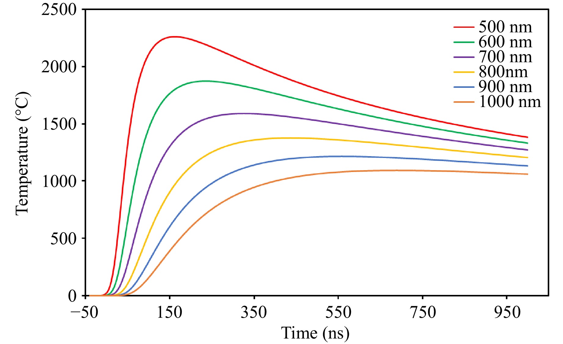
Fig. 7 Simulated back-side temperature evolution of SiOx films with thicknesses between 500 nm and 1000 nm under a laser fluence of 1 J cm−2.
These results imply that a minimum critical temperature at the back-side of the film is necessary to achieve stable adhesion to the receiver. Since the transferred films preserved their solid-state structure, it is reasonable to conclude that this threshold temperature is below the melting point of SiOx (Since glass lacks a sharp melting point, this term refers to the temperature at which significant structural changes occur). It should be noted that the simulation assumes idealized conditions where all absorbed energy contributes solely to heating and melting, neglecting energy losses associated with mechanical detachment processes, reflections, radiation, and scattering. Therefore, a precise quantitative determination of the critical back-side temperature remains beyond the scope of this model.
The simulation assumes idealized conditions, neglecting heat losses and interfacial effects. Nevertheless, it qualitatively illustrates how the maximum back-side temperature systematically decreases with increasing film thickness. This trend explains why thicker SiOₓ films require higher laser fluence to achieve sufficient adhesion: under identical irradiation, thinner films reach higher temperatures at the donor–receiver interface, which facilitates bonding. Hence, both experimental observations and thermal simulations consistently indicate that careful optimization of laser fluence, adapted to the film thickness, is critical for achieving stable and high-quality transfer in the LIFT process.
The experimental results indicate that for SiOₓ layers in the thickness range of approximately 200 nm to 1000 nm, printing at the optimum fluence yields strips with excellent quality and precise contour definition. Fig. 8 presents both scanning electron microscopy (SEM) and optical microscopy images of printed SiOₓ strips on fused silica substrates at three different thicknesses. Similar results were observed for BK7 substrates, as shown in Fig. S2. As depicted in Figures 8a–f, the printed strips with thicknesses between approximately 500 nm and 1000 nm exhibit exceptional precision and finely resolved structures. The lateral boundaries of the printed SiOₓ lines remain well-defined and sharp across all tested thicknesses, indicating that the transfer process does not introduce edge distortion or spreading. Comparable high-quality results were also obtained for thinner strips, down to approximately 200 nm, confirming the efficacy of the process across a wide range of film thicknesses.
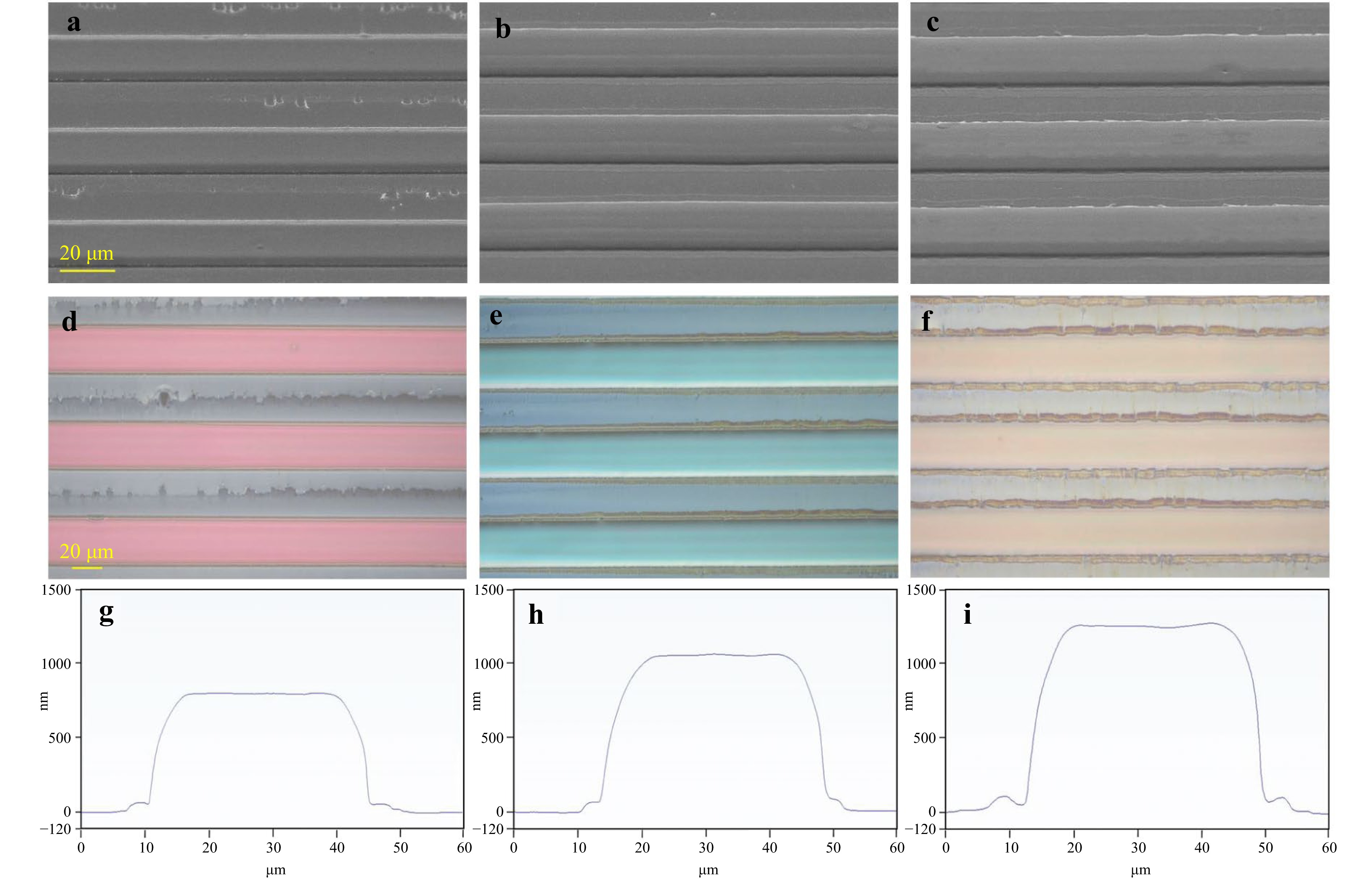
Fig. 8 a-c SEM images taken at a 60° tilt angle, d-f-) optical microscopy images, and g-i line profile analysis of printed SiOx strips on fused silica substrates. The SiOx layer thickness increases from left to right: 486 nm, 705 nm, and 950 nm. The measured profile height includes both the SiOx film thickness and the air gap between the printed film and the substrate. Note that the apparent line width in the SEM images is reduced due to the projection geometry caused by the tilt.
The transferred SiOₓ film thickness on the receiver substrate closely follows the original donor film thickness, as confirmed by surface profilometry (Fig. 8g-i). This volume-conserving behavior is further supported by the cross-sectional SEM images shown later in Figures 10a and 10b, where the printed layer thickness after transfer is nearly identical to the initial donor layer thickness observed under sub-threshold conditions.
In contrast to the successful transfer of SiOx films with thicknesses greater than 200 nm, the images of the 184 nm thick film presented in Fig. 9a, b show significant structural degradation. These observations are consistent with the intrinsic thermal limitations of the LIFT process. Numerical temperature simulations and experimental results from our previous works23,36 indicate that the temperature resulting from laser absorption reaches the melting point within this depth, leading to a low-viscosity and mechanically unstable phase throughout the entire film volume. It has been determined that, at laser fluences sufficient for film detachment, the region within the SiOx film that exceeds the melting temperature typically extends to a depth of around 200 nm. For films thicker than this critical depth, the residual portion remains solid and acts as a mechanical support layer, enabling stable and congruent transfer. In contrast, sub-critical films lack this solid base and are therefore prone to diffluence, deformation, or fragmentation during the transfer process. These findings define a practical minimum film thickness of approximately 200 nm for successful transfer under the given LIFT conditions.
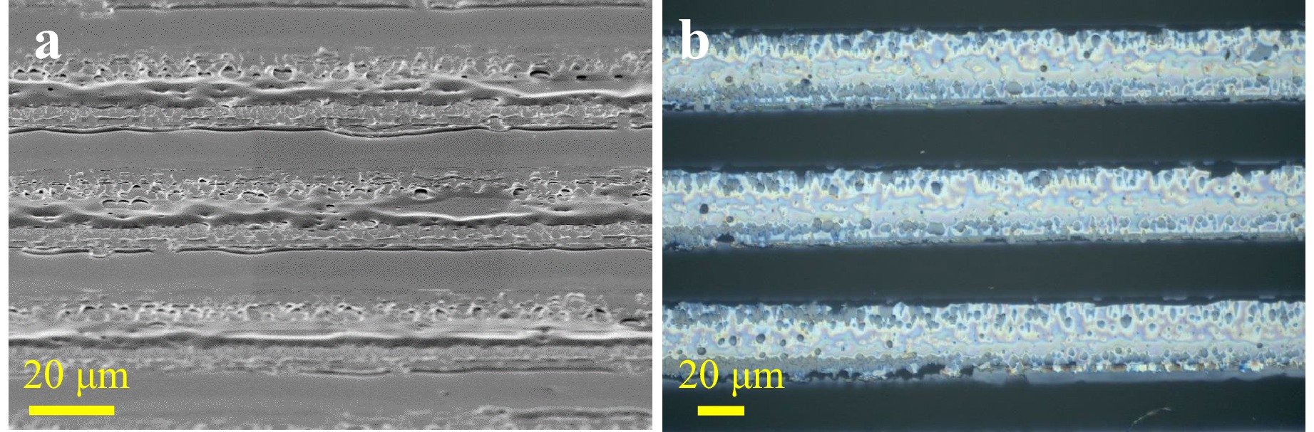
Fig. 9 a SEM (taken at a 60° tilt angle) and b optical microscopy images of printed SiOx strips on fused silica with a thickness of 184 nm. The apparent width of the printed lines in the SEM image is reduced due to projection geometry.
-
Fig. 10a presents a cross-sectional view of a SiOx strip (486 nm thick) deposited on a fused silica carrier substrate after laser irradiation under conditions suitable for complete transfer. In contrast, Fig. 10b depicts a comparable strip under a slightly sub-threshold fluence, just below the value required for full film separation. The morphology captured in these images reveals crucial insights into the delamination and transfer process. Notably, the detachment of the film initiates at the lateral edges of the irradiated strip. This edge-first delamination behavior is consistent with the thermal dynamics of nanosecond laser pulses. As previously discussed in Section 3.2, thermal simulations indicate that during the ~25 ns laser pulse, only a thin sub-layer of the SiOx film, approximately 200 nm thick, reaches temperatures sufficient for melting or partial vaporization. The upper portion of the film remains solid, resulting in a vertically stratified structure composed of a molten or vaporizing base layer below a mechanically stable intact solid layer. The resulting localized thermal expansion and transient vapor/plasma pressure generate significant stress at the donor-carrier interface. Two primary physical factors govern the onset of delamination:
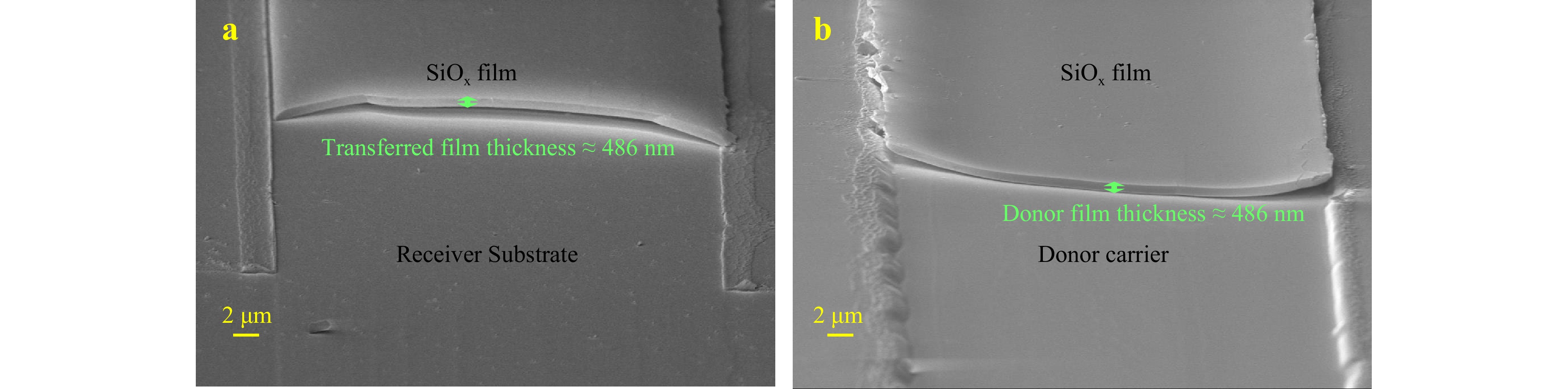
Fig. 10 Cross-sectional SEM images: a full transfer of a 486 nm thick SiOx strip to the receiver substrate at optimum fluence, and b incomplete separation under sub-threshold fluence, with the strip remaining partially attached to the donor carrier. Thickness indicators denote the SiOx film thickness on both the donor and the transferred sides.
1. Steep lateral thermal gradients (~30 μm strip width): The abrupt temperature drop between the heated strip and the adjacent cooler regions induces high thermomechanical stress at the edges. These edge zones act as preferential sites for micro-crack formation, which subsequently serve as nucleation points for delamination.
2. Narrow donor–receiver gap (~0.8 μm): Although beneficial for clean transfer, the limited vertical spacing restricts upward bulging, thereby intensifying stress accumulation at the lateral edges. This stress is preferentially released through crack initiation and lateral material displacement, as observed in the recorded images. Following crack formation, molten material is driven toward the edges under the combined influence of internal vapor pressure and surface tension. This migration results in localized accumulation, producing the characteristic edge curvature seen in the transferred structures.
As shown schematically in Fig. 11, the vapor pressure drives the propagation of the delamination front. Eventually, the film separates entirely from the carrier and adheres to the closely positioned glass receiver substrate, where it stabilizes due to surface energy and adhesion forces. This edge-initiated mechanism aligns with the theoretical model proposed by Meshcheryakov et al.37, who demonstrated that bending waves in laser-irradiated thin films deposited on rigid substrates (e.g., fused silica) originate at the strip edges.
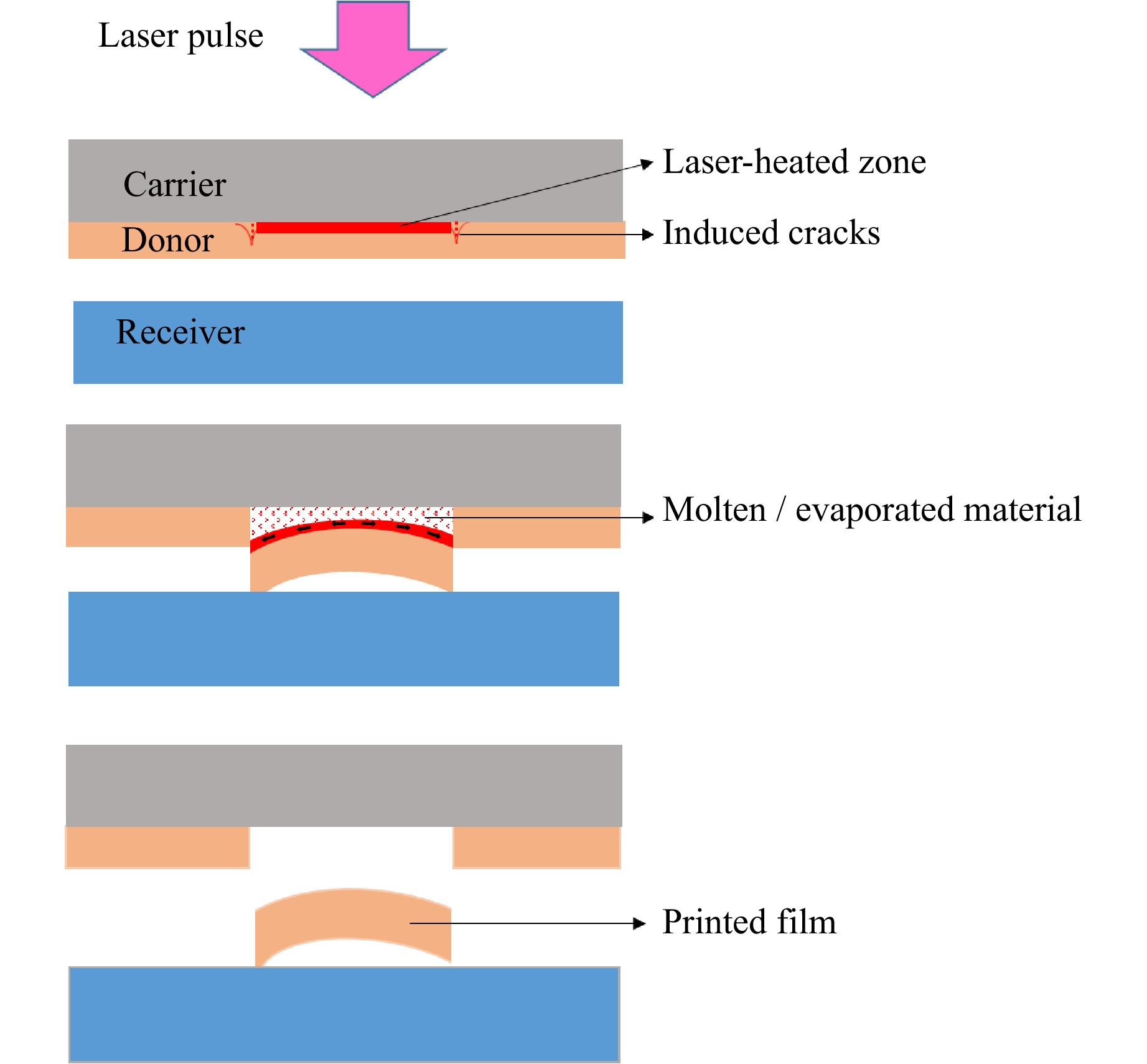
Fig. 11 Schematic of the proposed mechanism for thermally induced delamination and transfer of SiOx films via LIFT.
In summary, these observations confirm that in strip-beam LIFT with sub-micron gap distances, edge-induced delamination is not only probable but also inherent to the stress relaxation pathway, enabling controlled and directional transfer of SiOx films.
-
One of the key applications of the laser-induced forward transfer (LIFT) technique presented in this study is the fabrication of binary phase masks (BPMs). These masks are essential components in wavefront shaping and diffractive optics, used in beam shaping, optical filtering, and interferometric applications. Unlike amplitude masks that modulate light intensity, BPMs rely on spatial phase modulation of the wavefront to control the diffraction pattern, all while preserving optical power38,26.
In this study, a binary phase mask was fabricated by additively printing SiOₓ lines onto transparent fused silica substrates using the LIFT technique. The structure was designed with a duty cycle of 0.5, corresponding to equal line and space widths of 30 μm. As shown in Fig. 12a-c, SEM and optical microscopy images, along with surface profilometry analysis, collectively confirm the high uniformity and surface flatness of the printed SiOₓ lines. These features are critical for achieving precise and consistent phase modulation across the grating area. The periodic height modulation of the printed structures introduces a spatial phase shift, enabling the line-by-line construction of phase gratings with high fidelity. The resulting phase difference is defined by the pre-determined film thickness. Due to the optical transparency of SiOx in the visible spectral range, the printed mask can be used directly for visible-light applications without additional processing. The functionality of the BPM is demonstrated in Fig. 12d, which shows the diffraction pattern produced by a HeNe incident on the printed grating. A 632.5 nm HeNe laser was utilized in this study due to its well-established use as a standard monochromatic light source and its superior coherence characteristics39. As a standard source in optical metrology, the HeNe laser provides a highly stable, single-wavelength emission with an extremely narrow spectral linewidth, which enables precise and reproducible phase-sensitive measurements. In addition, its excellent spatial and temporal coherence ensures the formation of well-defined interference and diffraction patterns with high contrast, which is essential for accurately evaluating the performance of binary phase masks. Furthermore, the chosen wavelength lies within the optical transparency window of the SiOₓ films, allowing clean phase-based modulation without unwanted absorption effects. By selecting an appropriate film thickness a phase shift of π is achieved between adjacent zones, resulting in efficient suppression of the zero-order beam and enhancement of the ±1 diffraction orders. The required film thickness for achieving a π phase shift is derived from the relation27:
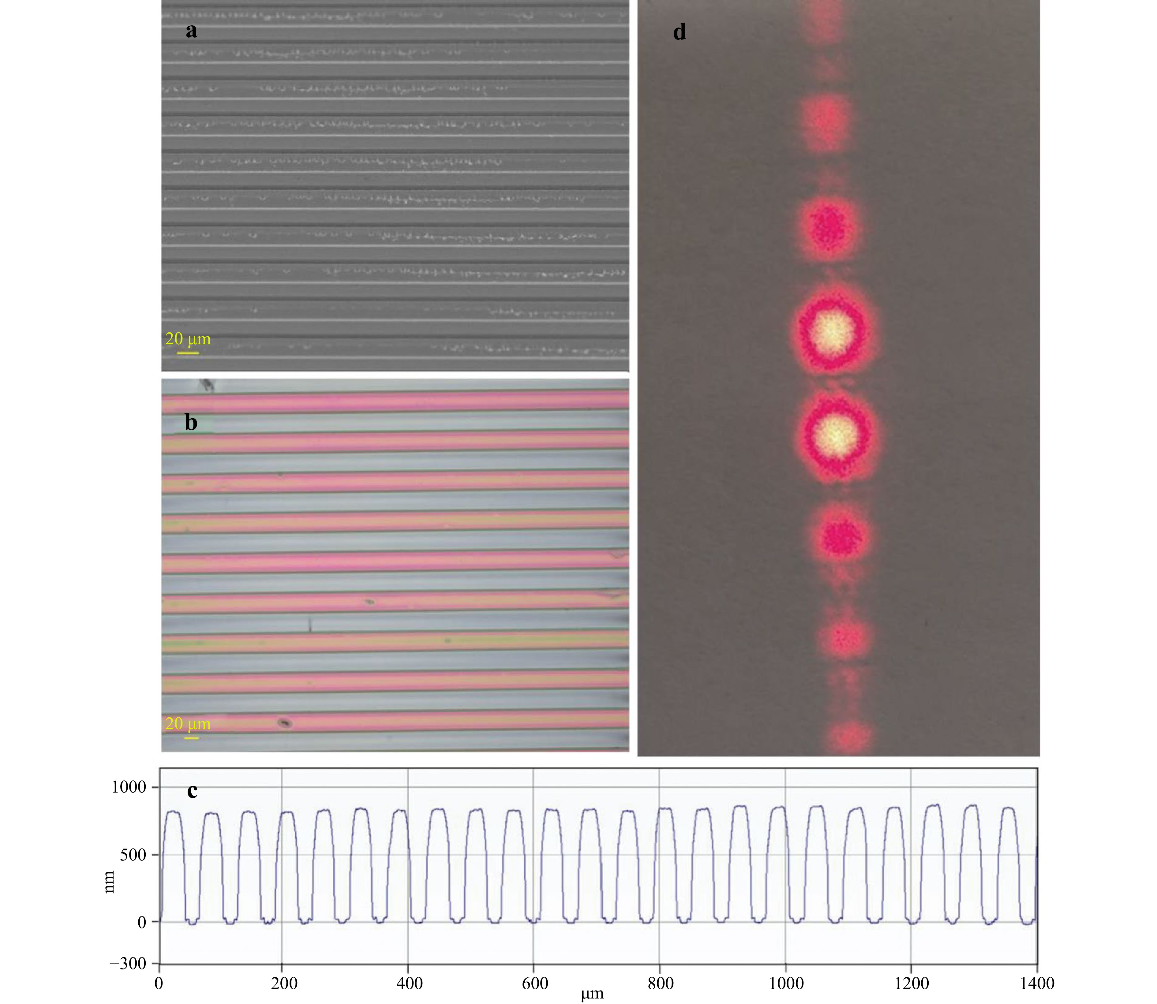
Fig. 12 a SEM image, b optical microscopy image, and c surface profilometry analysis of a binary phase mask fabricated by LIFT with a 30 μm period and a 0.5 duty cycle (the profile height includes both the film thickness and the printed film-receiver gap). d Diffraction pattern of a HeNe laser beam (λ = 632.5 nm) generated by the fabricated binary phase mask.
$$ d=\frac{\lambda }{2\left(n-1\right)} $$ where d is the thickness required to introduce a π phase shift, $ \lambda $ is the wavelength of the incident light (632.5 nm) and n the refractive index of SiOₓ (approximately 1.7). This d ≈ 452 nm, which closely matches the experimentally used thickness (486 nm). The resulting diffraction pattern confirms effective phase modulation, with measured diffraction efficiencies of 35.8% and 35.9% in the +1 and –1 orders, respectively. These values are close to the theoretical maximum of 40.5% for a perfect binary phase mask. The 0th order intensity appeared visually minimal, indicating successful suppression.
These observations suggest that the transferred SiOₓ films retain their stoichiometry and density during the LIFT process. The excellent agreement between the measured and theoretical diffraction efficiencies, which are highly sensitive to variations in refractive index and film thickness, implies minimal deviation of the material’s optical properties. Such stability would be unlikely if significant oxidation, porosity formation, or structural degradation had occurred during transfer. This interpretation is further supported by the dense and smooth morphology observed in cross-sectional SEM images (Fig. 10). Since the LIFT transfer proceeds in solid-state mode, using single-pulse irradiation and showing no observable melting or decomposition, substantial changes in film composition or structure are not expected.
For ultraviolet (UV) applications, fused silica is recommended as the receiver substrate. The printed SiOx lines can be thermally oxidized at high temperatures to form fully oxidized SiO2, ensuring high optical transparency in the UV range. Fig. 13 shows optical microscopy images of the phase grating before and after thermal treatment. The printed SiOx structures were successfully converted into transparent SiO2 while preserving their periodicity and structural integrity, an essential requirement for high-performance diffractive optics. The corresponding increase in UV transmission after thermal oxidation is confirmed by the measurements in Fig. S1.
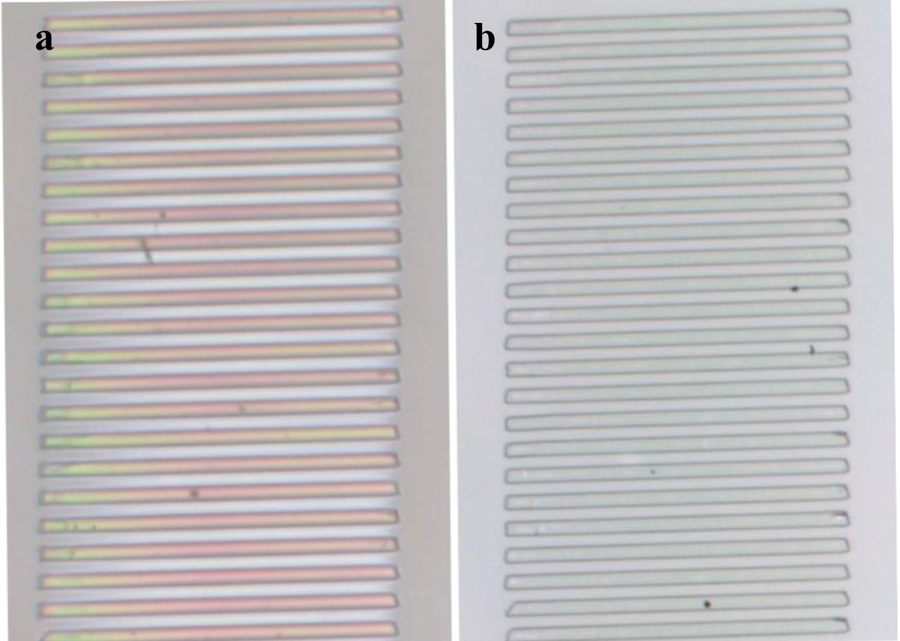
Fig. 13 Optical images of a printed SiOₓ-based binary phase mask (486 nm thick): a before and b after thermal treatment.
-
Despite the inherent fragility of the printed SiOx films particularly due to their sub-micron thickness and the additive nature of their deposition the binary phase masks exhibited excellent mechanical stability during the cleaning tests.
As shown in Fig. 14, optical microscopy images captured after each cleaning method indicate that all three treatments successfully removed surface contamination, including visible particles, without disrupting the printed structures. The blow-off method with nitrogen proved effective in removing loose particles, while the “drag wiping” method eliminated residual contamination. The immersion procedure yielded the most uniformly clean surface.
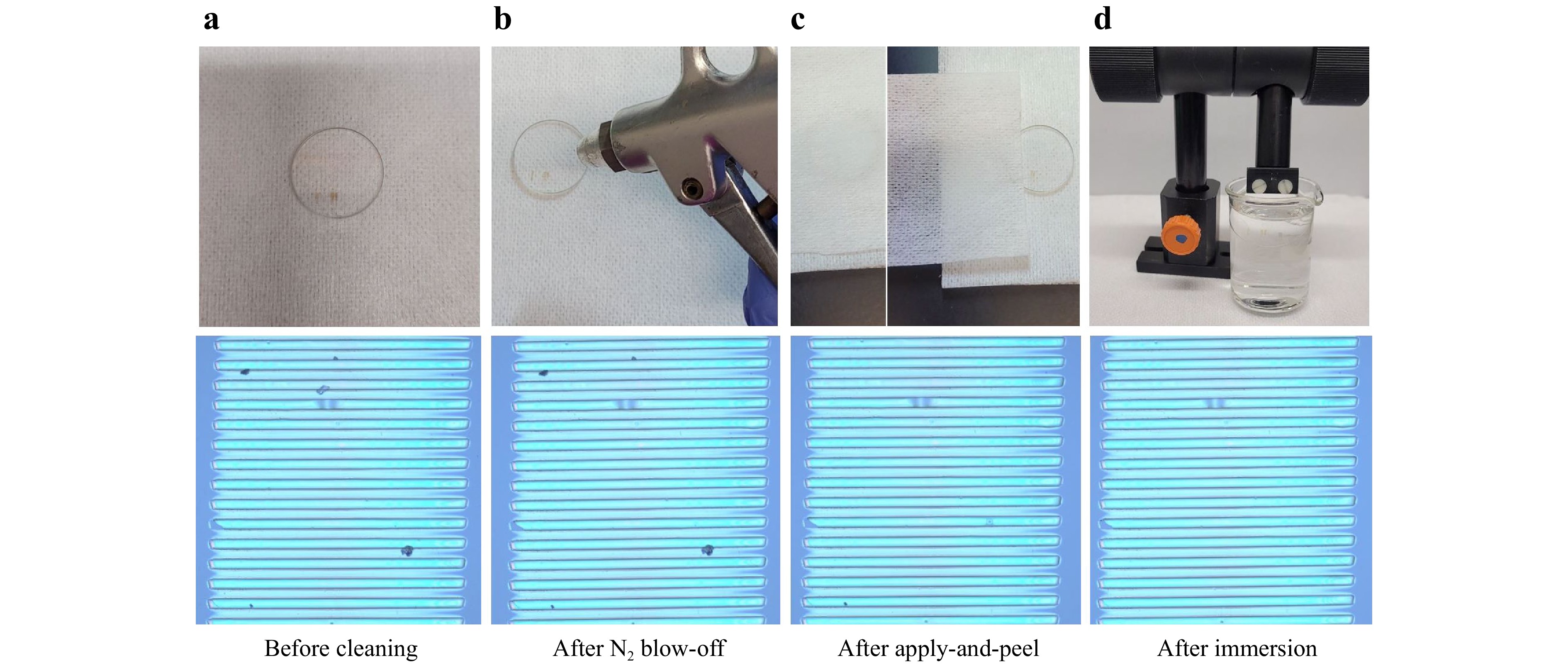
Fig. 14 Cleaning procedures and mechanical stability of printed 700 nm SiOx phase mask. Top: Photograph of each cleaning condition, bottom: corresponding optical microscopy (OM) image after the procedure. a As-printed sample before any cleaning. b Blow-off with nitrogen gas (~2 bar). c Drag wiping using acetone-wetted wipes. d Immersion in acetone for 2 minutes.
Crucially, no delamination, cracking, or displacement of the printed SiOx lines was observed under any of the treatments, confirming the robustness of their adhesion and structural stability. This highlights the potential of the fabricated phase masks for use in real-world optical systems, where occasional non-invasive cleaning may be required.
-
In this study, we demonstrated the feasibility of high-precision solid-state glass-on-glass printing of SiOₓ films using laser-induced forward transfer (LIFT) with single-pulse UV excimer laser irradiation at 248 nm in rear-side configuration. A mechanically optimized compression system minimized the donor–receiver gap to submicron levels, enabling clean and crack-free transfer onto fused silica and BK7 substrates. The process showed strong dependence on film thickness and laser fluence, with a critical thickness around 200 nm and an optimal fluence window ensuring structural integrity. We further applied this method to fabricate binary phase masks (BPMs) directly on glass, which exhibited excellent optical performance including efficient diffraction. Subsequent thermal oxidation converted the SiOₓ into transparent SiO2, making the components compatible with UV optics. The printed structures also showed strong adhesion and robustness under repeated cleaning cycles.
Compared to conventional LIFT and lithographic techniques, our approach is maskless, solvent-free, and etch-free, and allows direct patterning of UV-grade micro-optics on glass without cleanroom infrastructure. This work thus establishes a scalable and contamination-free route for fabricating advanced glass-based photonic components.
-
This work was supported by the Deutsche Forschungsgemeinschaft (DFG) under project number IH 17/28-1. The authors gratefully acknowledge Dr. Lukas Janos Richter for his valuable contribution in preparing the silicon suboxide-coated substrates used in this study. In addition, they gratefully acknowledge Dr. Jörg Meinertz for his valuable contribution to the numerical simulations.
High-precision glass-on-glass printing via laser-induced forward transfer of solid state sioₓ: fabrication technique and optical applications
- Light: Advanced Manufacturing , Article number: 8 (2026)
- Received: 14 May 2025
- Revised: 05 December 2025
- Accepted: 10 December 2025 Published online: 16 March 2026
doi: https://doi.org/10.37188/lam.2026.008
Abstract: Additive manufacturing of glass with submicron resolution remains challenging due to the intrinsic hardness, brittleness, and weak light absorption of most glasses. Here, we demonstrate the laser-induced forward transfer (LIFT) of substoichiometric solid-state silicon oxide (SiOₓ, x < 2) films for precise glass-on-glass printing. Using single-pulse 248 nm UV excimer laser irradiation and a custom-designed compression system, we achieve submicron donor−receiver gaps, enabling clean and crack-free transfer onto transparent substrates such as fused silica and borosilicate glass (BK7). In particular, the direct printing of SiOₓ onto fused silica substrates presents considerable challenges due to their high surface hardness and sensitivity to thermal stress. These factors often lead to poor adhesion and fragmentation of the transferred layers in conventional LIFT setups. We overcome these issues by implementing near-zero gap conditions and optimizing the laser fluence relative to the film thickness, enabling stable, residue-free transfer of SiOₓ onto fused silica. Systematic analysis reveals a strong dependence of transfer quality on both layer thickness and laser fluence, identifying a critical minimum thickness (~200 nm) and a narrow optimum fluence window. Furthermore, we use this approach to fabricate high-quality binary phase masks (BPMs) directly on glass, which exhibit well-defined π phase shifts and efficient diffraction under HeNe laser illumination. Post-deposition thermal oxidation transforms the transferred SiOₓ into fully transparent SiO2, making the structures suitable for UV optical applications. The resulting components demonstrate excellent mechanical robustness and resistance to standard cleaning procedures. This work establishes a solid-state pathway for fabricating functional glass-based micro-optical elements via LIFT.
Research Summary
Solid-state laser printing of glass-on-glass micro-optics
We demonstrate a solid-state laser printing method that writes silicon-oxide films directly onto glass with submicron precision. Using single UV pulses and a near-zero gap, the process cleanly transfers material without melting or residues, enabling robust, transparent microstructures and scalable fabrication of glass photonic components.
Rights and permissions
Open Access This article is licensed under a Creative Commons Attribution 4.0 International License, which permits use, sharing, adaptation, distribution and reproduction in any medium or format, as long as you give appropriate credit to the original author(s) and the source, provide a link to the Creative Commons license, and indicate if changes were made. The images or other third party material in this article are included in the article′s Creative Commons license, unless indicated otherwise in a credit line to the material. If material is not included in the article′s Creative Commons license and your intended use is not permitted by statutory regulation or exceeds the permitted use, you will need to obtain permission directly from the copyright holder. To view a copy of this license, visit http://creativecommons.org/licenses/by/4.0/.

 DownLoad: