


-
Periodic arrangements of subwavelength pores form the foundation of artificial all-dielectric nanophotonic structures, enabling exceptional control and manipulation of light1. Such integrated optical elements encompass diverse functionalities, from photonic crystals to metamaterials, surpassing the performance limits of conventional refractive optics2–5. High-performance nanophotonic devices (e.g., photonic crystals and metasurfaces) achieve revolutionary light manipulation via precisely engineered subwavelength architectures, demonstrating vast potential in optical communications, ultrasensitive sensing, advanced imaging, and quantum technologies6–9. The core performance of these devices, particularly for broadband, achromatic, and large-area functionalities, critically relies on constituent units possessing extreme depth-to-diameter ratios (typically >> 1 000:1)10. Photonic crystals derive functionality from wavelength-scale dielectric units (typically half-wavelength dimensions) arranged periodically11, this periodicity generates photonic bandgaps via Bragg scattering, selectively inhibiting propagation at specific frequencies. Enhanced micropore depth strengthens light-photonic crystal coupling, significantly augmenting device functionality. In contrast, metasurfaces depend on densely packed subwavelength units (typically <λ/5), such as metallic or high-index dielectric nanostructures. Achieving efficient, broadband, low-loss wavefront control—especially for achromatic operation—demands ultrahigh depth-to-diameter ratios to satisfy stringent phase dispersion requirements, which scale linearly with aspect ratio12.
Practically, nanophotonic devices show broad applicability in optical communications, information processing, and sensing. Specifically, this work achieves deep pores with an exceptionally high aspect ratio (>5 000:1). Such structures enable diverse functionalities, including: enhanced capacitance for dynamic random-access memory (DRAM); improved performance in thermoelectric devices; and reduced optical losses in devices that directly convert light into electricity via the photovoltaic effect13, additionally, high-aspect-ratio structures on optical device surfaces can significantly boost light absorption. In sensing applications, increased pore depth substantially enlarges the interaction volume with target substances, leading to a sensitivity to refractive index changes that is over 100 times higher compared to shallow pores14–16. However, realizing such structures presents significant challenges: maintaining nanoscale aperture uniformity and sidewall uniformity over centimeter-scale areas demands extremely high fabrication precision17. Currently, no technique exists that simultaneously delivers high depth-to-diameter ratios, large-area fabrication, and good structural repeatability for instance, while laser-induced periodic surface structures (LIPSS) dominate as the mainstream technique for large-area periodic nanostructuring, with established applications in materials science and laser technology18, their self-assembly nature results in irregular periodicity and poor controllability. This causes strong optical scattering and high losses, critically limiting device performance19,20. Among advanced lithography techniques, electron beam lithography (EBL) is considered highly promising due to its capability to fabricate diverse structures with high depth-to-diameter ratios and high regularity, including hierarchical architectures21,22. Nevertheless, EBL is applicable only to a limited range of materials and is primarily suited for simplified (non-complex) parallel patterning; furthermore, its patterning capability is strongly dependent on the initial master template21,22. Although conventional lithography and etching have propelled nanophotonics, technologies simultaneously achieving high-aspect-ratio nanostructures with large-area reproducibility remain scarce. Two-photon polymerization lithography achieves <50-nm resolution in 3D nanostructures, yet photopolymerization inherently incorporates photoinitiators that compromise mechanical rigidity23,24. This limits structural stability in high-aspect-ratio architectures while suffering from low throughput and high costs. Conventional high-aspect-ratio pores employ Bessel beams generated via conical wavefront intersection using axicons or spatial light modulators, or alternatively, azimuthally polarized beams. Bessel beams’ non-diffracting nature and extended depth-of-focus offer potential for high-aspect-ratio drilling25–28. However, depth-to-diameter ratios rarely exceed 200, with pore diameters exhibiting severe positional variations29. Micro-explosion mechanisms create porous sidewalls and inhomogeneities. Stress accumulation and pronounced side-lobe effects further restrict minimum inter-pore spacing, precluding dense, high-fill-factor nanohole array over large areas30. Threshold effects coupled with focal energy distribution fundamentally limit achievable depths, making depth-to-diameter ratios >1 000 impractical. Minor energy fluctuations beyond threshold are amplified by nonlinear scattering, inducing longitudinal inhomogeneity. Recent advances31,mitigate this by tailoring core-to-lobe energy ratios via annular binary masks, enhancing core energy at the expense of aspect ratio and reducing core contrast from 16% to 4%.
Thus, rapid fabrication of high-aspect-ratio, high-density periodic nanostructures remains a fundamental challenge for glass/crystal-based nanophotonics. Addressing this, Sun Hong-Bo’s group (Tsinghua University, 2019) demonstrated liquid-assisted femtosecond laser writing of silica microlens arrays with sub-3-nm roughness32. Their 2024 “super-stealth dicing” technique33 leveraged backscattering-interference feedback to achieve uniform longitudinal energy deposition and subwavelength transverse confinement, enabling 10-nm-scale cuts with depth-to-diameter ratios of 1 000–10 000. Concurrently, Srijoyee et al.34 reported single-step maskless fabrication of hollow nanochannel arrays in silica using tailored micro-Bessel beams, achieving tunable lengths (≤30 μm) and submicron periodicities (≥0.7 μm) via pulse-duration tuning. Jun, L. et al. (SUSTech, 2024)35 utilized ultrafast Bessel beams to create etch-guiding modifications in glass, enabling V-groove formation and centimeter-scale micro-pyramid arrays with 50-μm periodicity. Nevertheless, these methods require >100 pulses per site33, exhibiting low efficiency and poor large-area uniformity. Escalating pulse energy demands at high depth-to-diameter ratios further encounter spatial light modulator damage thresholds, with no demonstrations exceeding depth-to-diameter >10 000:1.
Here we present a wet-etching-assisted single-pulse nanolithography (WESPN) technique for high-efficiency fabrication of large-area deep-nanohole structures, combining beam-stretched single-pulse femtosecond (BSSPF) laser modification with selective chemical etching. Innovatively, we harness spherical aberration to axially stretch the focal volume, After the interaction between the laser and the material, the triggered photoionization process highly localizes high-density electrons within nanoscale regions. This mechanism drives confined amorphization with negligible peripheral thermal damage, enabling densely packed nanohole lattices. Subsequent wet etching exhibits high selectivity for amorphous regions, yielding nanoholes with diameters ≈30 nm, high uniformity, and ultrasmooth sidewalls. Beyond high-aspect-ratio fabrication, this technique enables the creation of nanohole-clad waveguides—structures where light is guided through an unmodified crystalline core surrounded by a periodic nanohole lattice acting as a low-index cladding. These waveguides combine the advantages of 3D integration, enhanced light–matter interaction, and functional sensing capability, bridging ultrahigh-aspect-ratio nanofabrication with integrated photonic applications. In this work, the term nanohole-clad waveguide refers to a solid-core optical waveguide surrounded by an array of periodically distributed nanoholes fabricated via spherical-aberration-enhanced single-pulse femtosecond laser modification followed by selective wet etching. Unlike photonic crystal fibers or hollow-core waveguides, the light is guided through the unmodified crystalline core, while the surrounding nanohole lattice functions as a photonic cladding that modifies the modal field and provides strong light–matter interaction capabilities. Key advantages include: (1) full 3D processing capability; (2) Record depth-to-diameter ratios >50 000, extendable beyond laser power limits; (3) High-density integration (pitch <450 nm, fill factor >70%) over 25-mm2 areas (scalable to cm2); (4) Polarization-independent circularity. WESPN not only provides an alternative approach for designing and fabricating conventional porous nanophotonic components, but also holds particular promise for realizing emerging porous nanophotonic devices requiring high depth-to-diameter ratios, high-density integration, and large-area features.
-
For experimental validation, nanostructuring was performed using a diode-pumped Yb: KGW laser system (PHAROS PH2, Light Conversion) operating at 1030 nm wavelength, With the pulse duration fixed at 213 fs and the repetition rates set to 10 kHz, 200 kHz, and 1 MHz for experimental purposes. The laser beam was focused onto subsurface target positions through a high-numerical-aperture objective (NA = 0.55, 50× magnification, Nikon). The sample was translated at a scanning speed of 0.5 mm/s, controlled by a high-precision closed-loop stage system (Aerotech ABL1000 and ANT130-V) with a positioning resolution of <100 nm. Single-crystal sapphire (α-Al2O3) served as the processing substrate; to deliberately enhance spherical aberration effects, a 3-mm-thick yttrium aluminum garnet (YAG) window was optically contacted to the sapphire surface. This configuration induced controlled refractive-index mismatch at the interface, substantially elongating the focal volume along the optical axis to achieve localized energy redistribution. After laser modification, samples were etched in 40 wt% hydrofluoric acid (HF) at 25 °C for 60 ± 5 min, followed by DI water rinsing and ultrasonic cleaning. This process selectively removed laser-amorphized regions, yielding high-aspect-ratio nanoholes with well-defined contours. To test the repeatability of the holes, we use a wavefront camera (SID4, Phasics) to perform phase delay detection on holes with the same parameters. We employed a spherical-aberration-enhanced focusing strategy by directing a high-NA objective to focus femtosecond laser pulses at a substantial depth inside the sample. When the laser beam propagates through a refractive-index-mismatched interface, a deliberate and strong spherical aberration is introduced. The accumulated phase error can be expressed by the spherical aberration function:
$$ \mathrm{\phi }({\theta }_{1},{\theta }_{2},-\mathrm{d})=-\mathrm{d}~({\mathrm{n}}_{1}\cos {\theta }_{1}-{\mathrm{n}}_{2}\cos {\theta }_{2}) $$ (1) Where θ1 and θ2 denote the incident and refracted angles, respectively. This depth-dependent, angle-dependent phase mismatch suppresses the formation of a conventional diffraction-limited focal spot. Instead, constructive interference redistributes the focal energy along the optical axis, resulting in a significantly elongated focal region (Rayleigh length >100 µm). This extended focal volume enables high-aspect-ratio material modification within a single laser exposure.
-
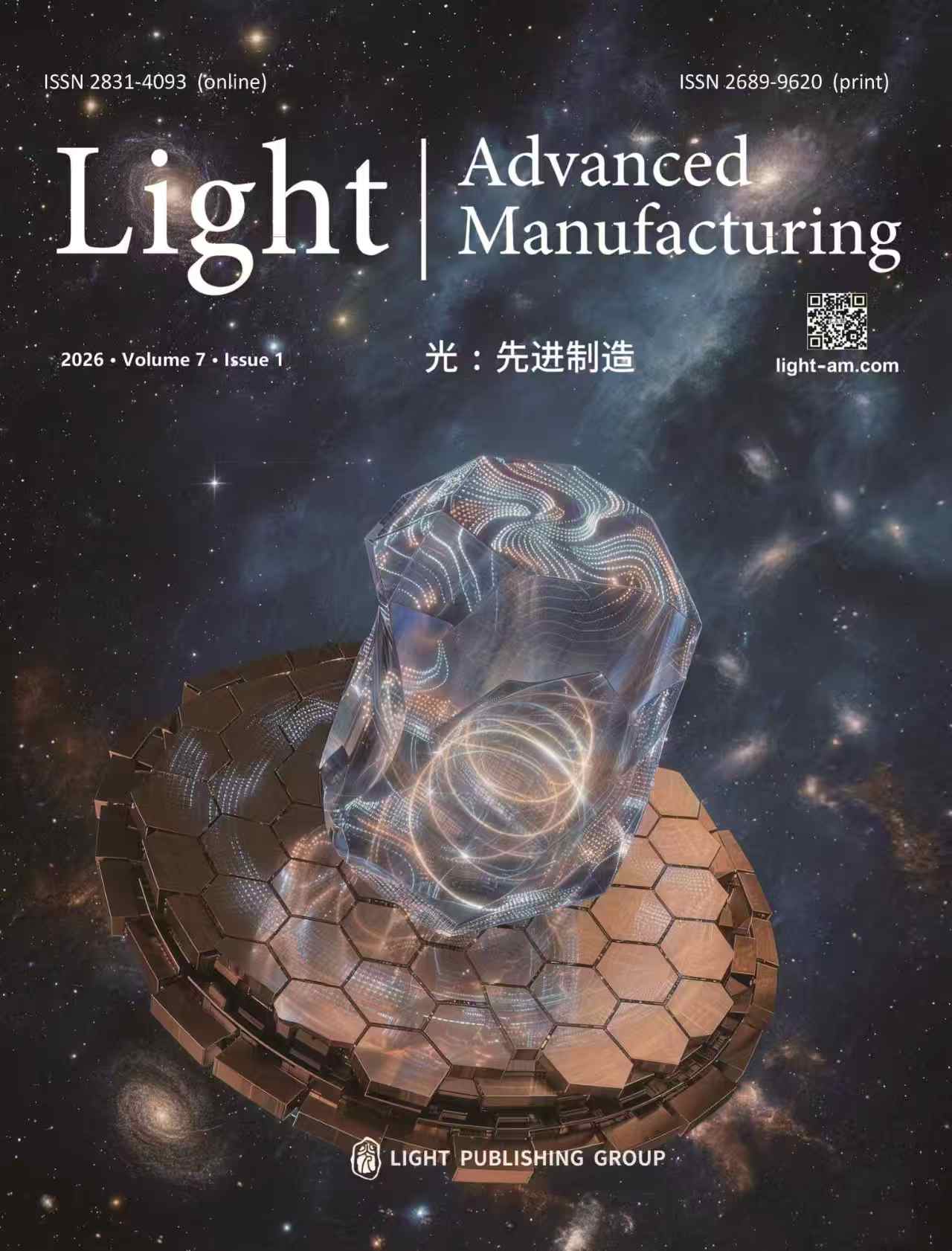
In this work, a spherical-aberration-enhanced technique was employed to fabricate Nanohole Cladding waveguides, where Fig. 1a schematically illustrates the fabricated Nanohole Cladding Waveguides structure. Spatially shaped femtosecond Gaussian pulses induced controlled modifications within the crystalline substrate, generating nanoholes with sub-500-nm diameters and lengths up to 200 μm. Side view of etched through-holes reveals improved smoothness relative to Bessel-beam drilling. Here, we present the simulated two-dimensional optical field distribution resulting from spherical-aberration enhancement (Distributed Light Field Schematics). Fig. 1b displays an image of the fabricated large-area Nanohole Cladding Waveguides, demonstrating centimeter-scale dimensions. This technique enables the fabrication of large-area, structurally complex, high-performance nanoporous devices. Spherical-aberration-enhanced BSSPF single pulses achieve nanoscale localized modification at arbitrary depths, ranging from the near-surface to the bulk region, within transparent sapphire substrates. Focal elongation redistributes energy axially, generating high-density ionization zones while confining the modified regions to the submicron scale (<400 nm). This non-thermal-dominated modification mechanism achieves breakthrough depth-to-diameter ratios >100 000 (depth >100 μm, diameter ~25 nm), surpassing conventional femtosecond laser processing limits (aspect ratio <1 000) by two orders of magnitude. Specifically, nanoholes exhibit independent control of nanohole diameter and depth: Diameter demonstrates strong pulse-energy dependence, with continuous control from sub-50 nm to 500 nm achieved by increasing the single-pulse energy from 3 μJ to 10 μJ. In the longitudinal dimension, through-holes can be formed by etching. Wet-chemical etching exhibits high selectivity for the laser-amorphized nanoscale regions, enabling the formation of high-aspect-ratio channels. Furthermore, the post-etch nanohole sidewalls exhibit low roughness, with internal surface smoothness meeting optical-grade requirements, ensuring precise morphological transfer. Phase-delay measurements of nanoholes fabricated under identical parameters (6.4 μJ, 1 MHz, 213 fs) show high reproducibility, with a phase variation of only 3.9% (Fig. 1c). Leveraging these controllability advantages enables expanded design capabilities. This technique facilitates the design of phase devices: Synchronized control of nanohole position (via programmed stage path) and diameter (via real-time pulse parameter tuning) on a monolithic substrate allows for the fabrication of structures such as gradient-phase metalenses.
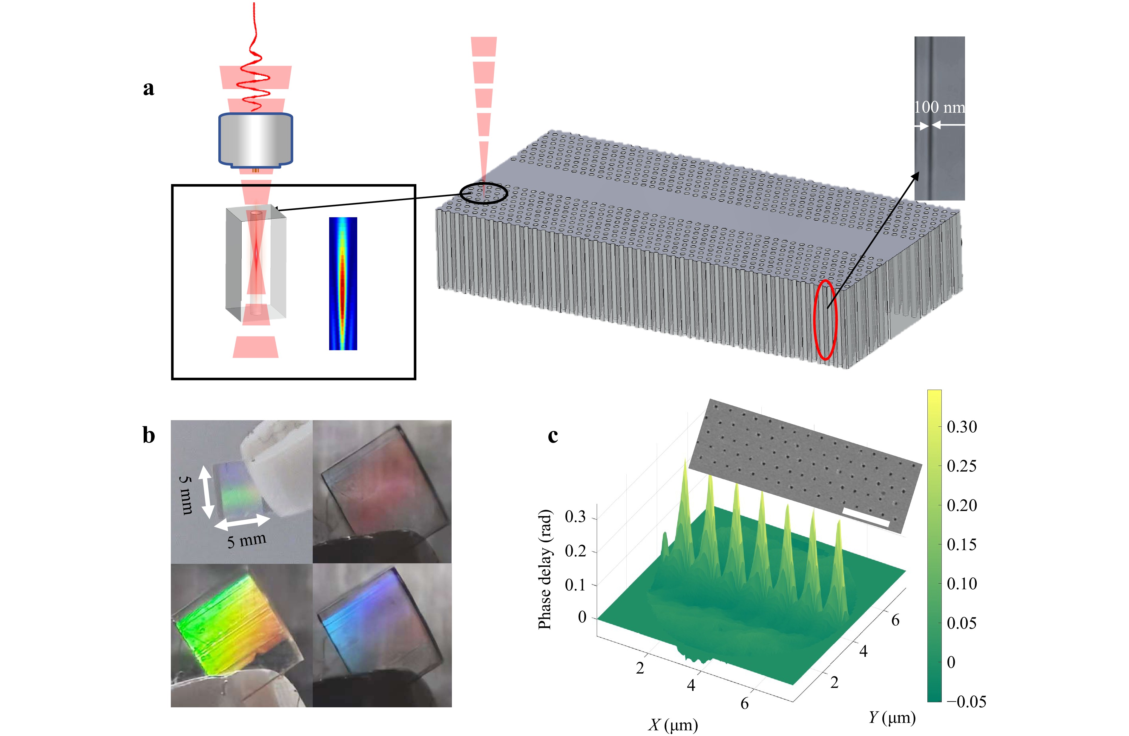
Fig. 1 Design and fabrication of the deep-nanohole-clad waveguide. a Schematic illustration of the fabrication process combining spherical-aberration-enhanced femtosecond laser modification and selective wet etching. The inset shows the simulated optical intensity distribution of the elongated focal volume. b Macroscopic photographs of the fabricated centimeter-scale sample exhibiting structural color. All panels share the same scale (Dimension: 5 × 5 mm2). c Phase-delay map indicating the high uniformity of the periodic structures (Scale bar: 3 μm).
In order to fabricate the large-area Nanohole Cladding Waveguides, we tested laser pulses with different parameters to obtain the corresponding length parameters of the fabricated apertures. Fig. 2a-c presents SEM-measured correlations between pulse energy and nanohole diameter, quantifying the influence of pulse repetition rate (Freq) and pulse number (Npulse) on laser-induced nanostructure dimensions. At fixed single-pulse energy, nanohole diameters exhibit significant variations with Freq and Npulse:
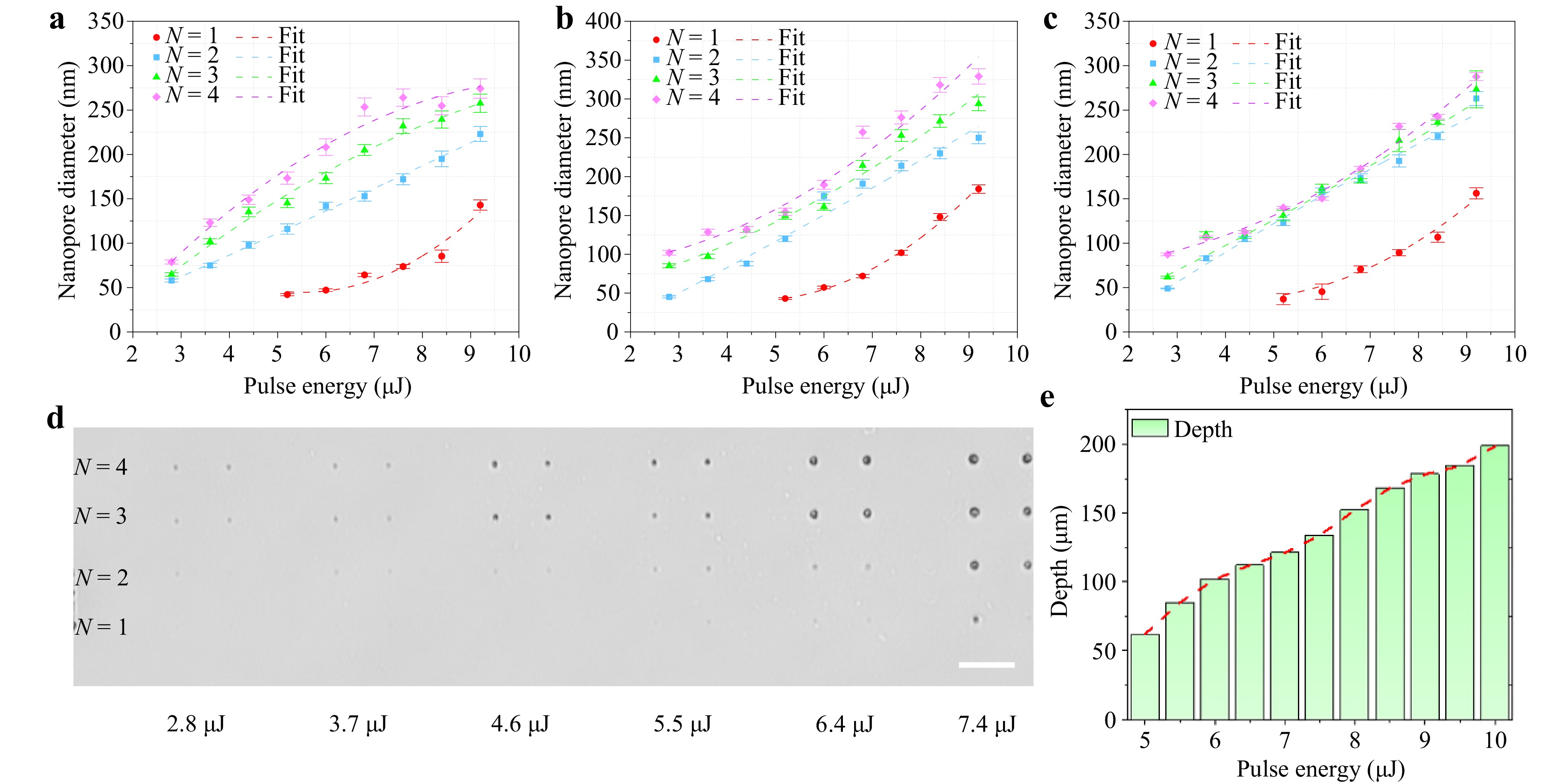
Fig. 2 Dependence of nanohole dimensions on laser processing parameters. a-c Variation of nanopore diameter with pulse energy at repetition rates of 10 kHz, 200 kHz, and 1 MHz, respectively. The data points represent different pulse numbers (N). d Optical microscopy images of the nanoholes fabricated under varying pulse energies and pulse numbers, showing the evolution of morphology. (Scale bar: 10 μm). e The correlation between hole depth and pulse energy at 5.5 μJ. All processing was performed with a scan speed of 0.5 mm/s and a pulse duration of 213 fs.
1. Multi-pulse mode (Npulse ≥ 2) as Freq increases from 10 kHz to 1 MHz, diameter data for identical Npulse progressively converge (Fig. 2a-c).
2. At 1 MHz (Fig. 2c), energy-diameter curves for 2−4 pulses become nearly superimposed, demonstrating that thermal accumulation dominates at high frequencies, thereby diminishing independent control via single-pulse energy.
Microscopy reveals that single pulses produce detectable modifications only when Epulse 4.6 μJ, whereas multi-pulse irradiation generates continuous structures at 2−8 μJ, with increasing pulse number substantially reducing the effective ablation threshold. Furthermore, single-pulse-induced nanochannel depth displays sublinear dependence on Epulse, where depth increment progressively decreases with rising energy, arising from nonlinear absorption saturation and enhanced plasma shielding that reduce energy transfer efficiency to deeper regions. Fig. 2d illustrates the morphological evolution of nanoholes observed under varying pulse energy and pulse number. A clear trend is observable: with increasing pulse number, the nanohole processing threshold shifts, and the diameter concurrently changes. Furthermore, as pulse energy increases, a significant enlargement in diameter is evident. Fig. 2e presents the influence of pulse energy variation on nanohole depth, when the pulse energy is increased from 2 μJ to 10 μJ, the nanohole depth increases from 60 μm to 200 μm, achieved on a 260-μm-thick sapphire substrate, demonstrating alignment with the aforementioned characteristic of independent control of nanohole diameter and depth.
Building upon the spherical-aberration-enhanced high-aspect-ratio nanohole fabrication technique, we introduce focal-stitching technology to further augment achievable depth-to-diameter ratios. Fig. 3a collectively demonstrates the innovative axial dynamic focal control strategy for extreme-aspect-ratio breakthroughs: Under constant single-pulse energy (5.5-10 μJ), discrete stepwise Z-axis translation via precision stages (80 μm per step) synchronizes focal depth advancement with the plasma channel front using position-synchronized output (PSO). At a nanohole diameter of 30 nm, this approach overcomes nonlinear absorption saturation and plasma defocusing, elevating the nanochannel aspect ratio from 5 000:1 (static focus) to 50 000:1 (depth 1 500 μm, diameter 30 nm). Furthermore, at a pulse energy of 5.5 μJ with stitching over an 80 μm step (Fig. 3b), nanoholes formed at different depths exhibit a coefficient of variation (COV) of merely 5.1% in length,numerical simulations further corroborate this depth insensitivity, confirming that the effective modification length, governed by the modification threshold, remains consistent throughout the fabrication depth. We hypothesize that this uniformity arises because elongation induced by enhanced spherical aberration counterbalances power attenuation when focusing deeper below the surface, resulting in nanoholes of approximately equal length across depths. Fig. 3c illustrates the stitching process where sequential upward Z-axis movement enables interconnection of adjacent nanoholes at sufficient energy, forming continuous high-aspect-ratio nanoholes. Fig. 3d demonstrates stitching efficacy near the threshold: stitching below threshold (right) fails to achieve continuous channels, whereas at the threshold energy, nanoholes connect longitudinally and form smooth interfaces at junction points.
Fig. 3 Strategy and characterization of dynamic axial focal stitching. a Stitching schematic and high-resolution SEM image. (Scale bar: 400 nm). b Depth-dependent nanohole length distribution at discrete axial positions. c Working principle of focal stitching. d Cross-section at energy-threshold transition zone (Scale bar: 150 μm). All processing was performed with a scan speed of 0.5 mm/s and a pulse duration of 213 fs, Z-axis movements were performed at a lift speed of 0.05 mm/s.
The proposed spherical-aberration-enhanced single-pulse modification strategy is not restricted to sapphire. Similar results can be achieved in other transparent dielectrics, such as quartz, fused silica, and some fluoride crystals, where sufficient etching selectivity exists. In polymers or thin films, due to their lower damage thresholds and different electron-phonon coupling dynamics, process optimization would be required, yet the principle remains valid.
We fabricated visible-wavelength Nanohole Cladding Waveguides with a uniform 1 μm pitch in both transverse and longitudinal directions, featuring 0.5 μm row-offset patterning. The central region incorporates a 6 μm isolation gap, yielding a total waveguide length of 5 mm using periodically arranged nanoholes (diameter: 150 ± 10 nm, pitch: 1 μm). The nanohole arrays act as a photonic cladding that modulates the local refractive-index distribution and provides lateral optical confinement for the guided mode within the central unmodified region.
Our waveguide employs a periodically arranged array of ultra-deep nanoholes as a lateral cladding, while the guiding core is defined by the unmodified sapphire region between adjacent nanohole columns. Although the geometry resembles a periodic lattice, the feature sizes used in this work are far below the wavelength scale and therefore do not produce a photonic bandgap. Instead, the structure operates entirely through index guiding, where the nanohole lattice forms a low-index cladding due to its large void fraction, and the sapphire core acts as the high-index guiding region. Importantly, the guided mode supported by our nanohole-clad waveguide does not experience radiation loss through coupling to unwanted slab-like TE modes36. This is primarily due to the high structural symmetry of the sapphire core and the nanohole cladding in both transverse directions. As a result, the symmetry of the field components of the dominant mode, analogous to a TM-like guided mode with a strong evanescent-field component in the cladding, is inherently orthogonal to the symmetry of the TE-type planar modes that typically arise in conventional ridge waveguides. This orthogonality prevents any significant modal coupling, ensuring that the guided mode remains well confined and low-loss while still providing strong evanescent-field interaction within the nanohole array. Electromagnetic simulations generated the waveguide's optical field distribution (Fig. 4a, left). A 1550-nm continuous-wave laser was coupled into the Nanohole Cladding Waveguides via optical fiber to characterize its mode field distribution. Top-view imaging under green light illumination clearly demonstrates the optical guidance characteristics of the structure (Fig. 4b), modal purity reached 10.90 dB. In the fiber-optic coupling platform experiments (Fig. 4c), the Nanohole Cladding architecture was independently excited by 1550 nm near-infrared and 532 nm visible laser sources. Light propagation profiles were captured using a short-wave infrared camera (Model: SWIR-500A1-U, LBTEK). Distinct waveguide-confined optical paths observed at both wavelengths conclusively demonstrate cross-band light-guiding functionality spanning the telecom C-band and visible regime. This study successfully validates the high-sensitivity sensing functionality of the nanostructure. Furthermore, to demonstrate the potential for flexible light routing beyond straight channels, we also fabricated a Z-shaped waveguide (Figure S4), which successfully guides light through distinct bending sections, verifying the 3D capability of this technique. Based on the fluorescence response characteristics of Rhodamine 6G in alcoholic environments37, we developed a specific sensor for ethanol molecules. Laser-modified and etched samples were immersed in 0.835 × 10⁻³ mol/L Rhodamine 6G-ethanol solution, utilizing capillary forces to drive probe molecules into the nanoholes. Through micro-Raman spectroscopy (Renishaw InVia confocal Raman spectroscope) detection at an excitation wavelength of 532 nm (Fig. 4d), we observed significant spatial fluorescence intensity distribution differences: In pore-free regions, fluorescence intensity approached background noise levels (<200 counts), In nanohole array regions, strong fluorescence signals emerged (>3 000 counts), with intensity distribution perfectly matching pore locations, and some reaching 10,000 counts. As pore depth gradually increased, more Rhodamine 6G molecules entered the pores, consequently enhancing ethanol sensitivity. This depth-dependent sensitivity enhancement originates from two mechanisms to improved molecular capture efficiency: Exponential growth of surface area increases molecular loading capacity; Nanoconfinement effects in porous materials: Within nanoholes, reduced dissociation and mass transport rates demonstrate strong confinement effects that trap molecules, with decreased molecular diffusion coefficient (due to increased collision frequency in confined spaces) prolonging probe-analyte interaction time38.
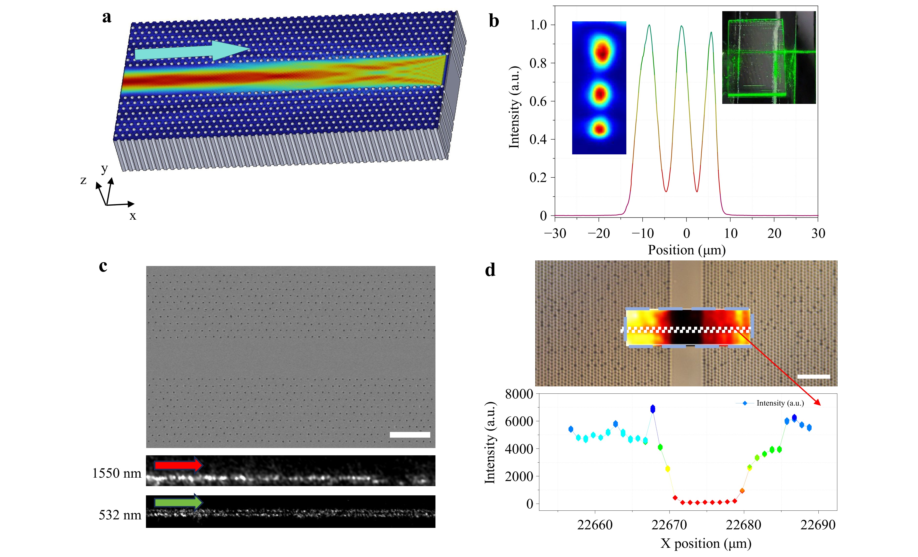
Fig. 4 Optical characterization and sensing performance of the nanohole-clad waveguide. a Simulation results of the optical field distribution in the nanohole-clad waveguide. b Optical measurement showing the mode intensity profile and the transmission image under green-light (532 nm) excitation. c Scanning electron micrograph of Nanohole Cladding Waveguides (top), planar near-field distribution under 1550 nm excitation (middle), and 532 nm visible-light-excited optical field captured by infrared camera (bottom) (Scale bar: 5 μm). d 1D and 2D Raman mapping results of the Nanohole Cladding Waveguides, along with microscopic images after soaking in Rhodamine 6G, the 2D Raman map is overlaid on the microscopy image for intuitive visualization of the results. (Scale bar: 10 μm).
Furthermore, this platform shows great promise for real-time environmental monitoring and biomedical diagnostics. For instance, it could be deployed as a highly sensitive on-chip ethanol sensor for evaluating alcohol concentration in biological fluids or monitoring fermentation processes in industrial bioreactors. The enhanced light-matter interaction within the nanoholes also opens avenues for detecting other trace analytes via functionalization with appropriate molecular probes.
-
In summary, we demonstrate a fabrication strategy that overcomes the long-standing depth limitation of single-pulse nanolithography by combining spherical-aberration-mediated focal stretching with dynamic axial stitching. This enables continuous nanoholes with record depth-to-diameter ratios exceeding 50 000:1 and ultrasmooth sidewalls. Leveraging this capability, we further establish a nanohole-clad waveguide architecture in sapphire, where a deep, low-index nanohole lattice provides robust lateral confinement and strong evanescent-field interaction. This unified approach offers a scalable route to functional photonic integration in hard crystalline substrates, opening new opportunities for quantum emitters, dense photonic circuits, and high-sensitivity biochemical sensing.
-
This work was supported by the National Natural Science Foundation of China (Nos. 12404367, 52432001); Natural Science Foundation of Zhejiang Province (Nos. LZ23F050002, LDG25F050001);
Deep-nanohole-clad waveguides with depth-to-diameter ratio up to 50 000 in single crystals via femtosecond laser writing
- Light: Advanced Manufacturing , Article number: 40 (2026)
- Received: 15 December 2025
- Revised: 05 March 2026
- Accepted: 18 March 2026 Published online: 17 April 2026
doi: https://doi.org/10.37188/lam.2026.040
Abstract: Femtosecond laser writing offers exceptional flexibility and spatial selectivity, enabling the customization of multifunctional integrated devices with nano-scale resolution. This study introduces a novel approach for fabricating nanohole-clad waveguides with ultra-high depth-to-diameter ratios using femtosecond laser writing combined with spherical-aberration-enhanced focal stretching and selective wet etching. This technique not only achieves record depth-to-diameter ratios (>50 000:1) with nanoholes (diameter: 30-500 nm, depth: 1 500 μm) but enables the creation of functional photonic waveguides. The integration of nanoholes into the waveguide structure provides a platform for multi-functional integrated devices, demonstrating significant tunable optical properties. By adjusting pulse energy and axial focal stitching, the diameter of the nanoholes can be tuned from 30 nm to 500 nm with high precision. Further, fluorescent probes embedded within the nanoholes provide a demonstration of optical sensing capabilities, as the waveguide effectively guides light to excite the probes, generating strong detectable signals. The submicron precision achieved through the process ensures high-quality waveguiding with 10.9 dB mode purity, while centimeter-scale periodic arrays exhibit excellent phase uniformity (deviation <3.9%). This work demonstrates the potential of femtosecond laser writing to directly fabricate high-aspect-ratio nanostructures and integrate functional photonic devices on substrates, opening up new possibilities for multi-functional photonics and sensor applications.
Research Summary
Nanophotonics: Laser-written deep nanoholes enable advanced crystal waveguides
Researchers have developed a novel laser technique to carve ultra-deep nanoholes into single crystals, creating functional photonic waveguides for advanced optical sensors and multi-functional integrated devices. Conventional fabrication methods struggle to simultaneously deliver high depth-to-diameter ratios, large-area fabrication, and structural repeatability. Jianrong Qiu, Lijing Zhong, and colleagues from Zhejiang University report a femtosecond laser method combined with spherical-aberration-enhanced focal stretching and selective wet etching. This approach achieves record depth-to-diameter ratios exceeding 50,000:1. The team created nanohole-clad waveguides that efficiently guide light and demonstrate highly sensitive sensing capabilities, such as detecting ethanol molecules, showing great promise for real-time environmental monitoring and biomedical diagnostics.
Rights and permissions
Open Access This article is licensed under a Creative Commons Attribution 4.0 International License, which permits use, sharing, adaptation, distribution and reproduction in any medium or format, as long as you give appropriate credit to the original author(s) and the source, provide a link to the Creative Commons license, and indicate if changes were made. The images or other third party material in this article are included in the article′s Creative Commons license, unless indicated otherwise in a credit line to the material. If material is not included in the article′s Creative Commons license and your intended use is not permitted by statutory regulation or exceeds the permitted use, you will need to obtain permission directly from the copyright holder. To view a copy of this license, visit http://creativecommons.org/licenses/by/4.0/.

 DownLoad: