


-
The rapid evolution of smartphone cameras and wearable AR glasses is driving demand for compact, high-performance imaging systems1–6. Near-infrared (NIR) imaging, which is essential for autonomous driving, medical diagnostics, and biometrics, supports deeper tissue penetration and improves low-light performance compared with visible-light modules7–11. However, miniaturised near-infrared optical modules face the major challenges of simultaneously achieving high imaging quality, an ultra-wide field of view (FOV), extreme compactness, and performance that exceeds that of conventional refractive optics. Even state-of-the-art aspherical lens stacks are bulky and costly, and advanced aspheric designs involve trade-offs among FOV, aberration correction, and system miniaturisation12–18. Emerging solutions such as metalenses and planar diffractive optics offer thinner devices and high spatial resolution, but suffer from off-axis aberrations, nonuniform illumination, and limited scalability for wafer-level production19–26. Hybrid metasurface-refractive systems have shown promise; however, current approaches typically rely on discrete lens designs that require additional mechanical support and precise post-fabrication alignment27–29. This reliance increases both the lateral dimensions and the assembly complexity, thereby limiting the development of lightweight, compact, and truly mass-producible modules. Furthermore, these discrete hybrid designs are inherently incompatible with standard wafer-level batch fabrication because accurately assembling discrete diffractive and refractive optics post-dicing is difficult and labour-intensive, restricting their scalability for real-world applications.
Thus, a key limitation is the absence of a robust wafer-level process for monolithically integrating refractive and metasurface elements, which must ensure precise alignment, structural stability, and compatibility with high-throughput manufacturing. Additionally, conventional hybrid diffractive-refractive designs do not account for the true dispersion characteristics of metalenses, resulting in a mismatch between the simulated and actual performances, particularly for imaging systems with a certain bandwidth.
Here, we address these challenges using a wafer-level-manufactured MAL pipeline that enables the monolithic integration of aspherical refractive lenses and metalenses on a single wafer, targeting narrowband NIR imaging with an ultrawide FOV for mobile applications. The MAL is realised by introducing an active-alignment (AA) mask method to bond the aspherical lens and metalens structures at the wafer level, achieving micrometre-level alignment accuracy and leaving an engineered air gap to maintain the integrity of the nanostructured metasurface. This design eliminates the need for additional mechanical support and complex post-fabrication alignment, compresses the module volume by an order of magnitude, and supports high-yield, wafer-scale mass production. Notably, our optical design process incorporates accurate modelling of metalens dispersion and process integration, and is capable of precisely calculating the accurate phase response of the metalens under various dimensions, such as different wavelengths and incident angles. This design allows the calculation of precise optical responses across the entire design bandwidth, enabling close agreement between the simulation and fabrication performance and overcoming the shortcomings of prior hybrid lens design approaches.
This integration attains a 101.5° FOV, a 3.39 mm total track length (TTL), an F/1.64 aperture, and a compact volume of 0.02 cm3, offering a substantial total volume reduction over previous hybrid designs while maintaining a modulation transfer function (MTF) exceeding 0.31 at 50 lp/mm, thus reaching the diffraction limit for small-pixel NIR sensors. The MAL achieved uniform relative illumination, over 90% central diffraction efficiency, and a close agreement between the optical simulations and the fabricated results. Unlike previous discrete designs, our approach achieved true monolithic integration, avoided lateral expansion, and ensured structural stability without auxiliary bonding. Compared with pure refractive and metalens-only systems, the MAL balances a wide FOV, high MTF, and ultracompact size more effectively. Moreover, compared with the designs of double-layer or multilayer metalenses, the MAL we designed is an improvement over the traditional refractive lens assembly. It can be optimised through geometric optical ray-tracing methods without the need for complex diffraction calculations and avoids the reduction in diffraction efficiency and uneven relative illumination caused by the introduction of multilayer metalenses.
We validated the MAL’s performance through direct NIR imaging of eye tracking and blood vessels, as well as computational super-resolution experiments, which integrate the deep learning model, a state-of-the-art neural network for pixel super-resolution, and highlighted the high compatibility and practical potential of our MAL platform for hardware-software co-optimised NIR imaging. Together, these advances offer a scalable wafer-level optical solution that connects high-performance NIR imaging with mass manufacturing, enabling new possibilities for next-generation mobile, AR/VR, and biomedical imaging devices.
-
A schematic diagram of the integrated imaging system is shown in Fig. 1a. This system combines a MAL imaging module and a subsequent image-restoration module. The MAL is responsible for encoding the target light field onto the sensor, whereas the image restoration module is designed to refine and enhance the spatial resolution of the acquired images. When tailored to increase the resolution of an image produced by the MAL imaging system automatically, the framework can independently generate a high-fidelity output image at 1K. In the entire imaging pipeline, the performance of the MAL design determines the quality of its direct imaging, the difficulty of computational deconvolution, and the overall volume and structural complexity of the imaging system. The designed MAL in this work has a TTL as low as 3.39 mm and a wide FOV of 101.5° within a minuscule volume (2.564 × 2.39 × 3.35 mm3). This advancement stems from our integrated hybrid lens design framework, shown in Fig. 1b. Unlike conventional hybrid lens systems assembled from discrete elements, our integrated MAL stack achieved micrometre-level alignment accuracy and intrinsic structural stability without auxiliary mounting hardware. The compact structure of the MAL, with a direct optical element connection, allows us to use wafer-level manufacturing technology for hybrid lens system batch production, facilitating low-cost, rapid manufacturing in large quantities. As shown in Fig. 1c, thousands of MALs can be fabricated simultaneously on an 8-inch wafer, enabling scalable manufacturing of high-performance microimaging systems. To demonstrate the ultracompact form factor of the wafer-diced MAL, we compared our MAL with a US one-dollar coin to visually demonstrate the extremely compact size of the lens, as shown in Fig. 1d. This lens has the potential for integration into smartphones and wearable AR glasses. As an application example, Fig. 1e shows that MAL can be seamlessly integrated into the Even Realities AR glasses platform without compromising the aesthetic design or user experience. An enlarged view of the fabricated MAL is shown in Fig. 1f, revealing an aspherical lens and a metalens bonded via glass. A protective cover glass was integrated into the module with an air gap to avoid damage to the nanopillars on the metalens.
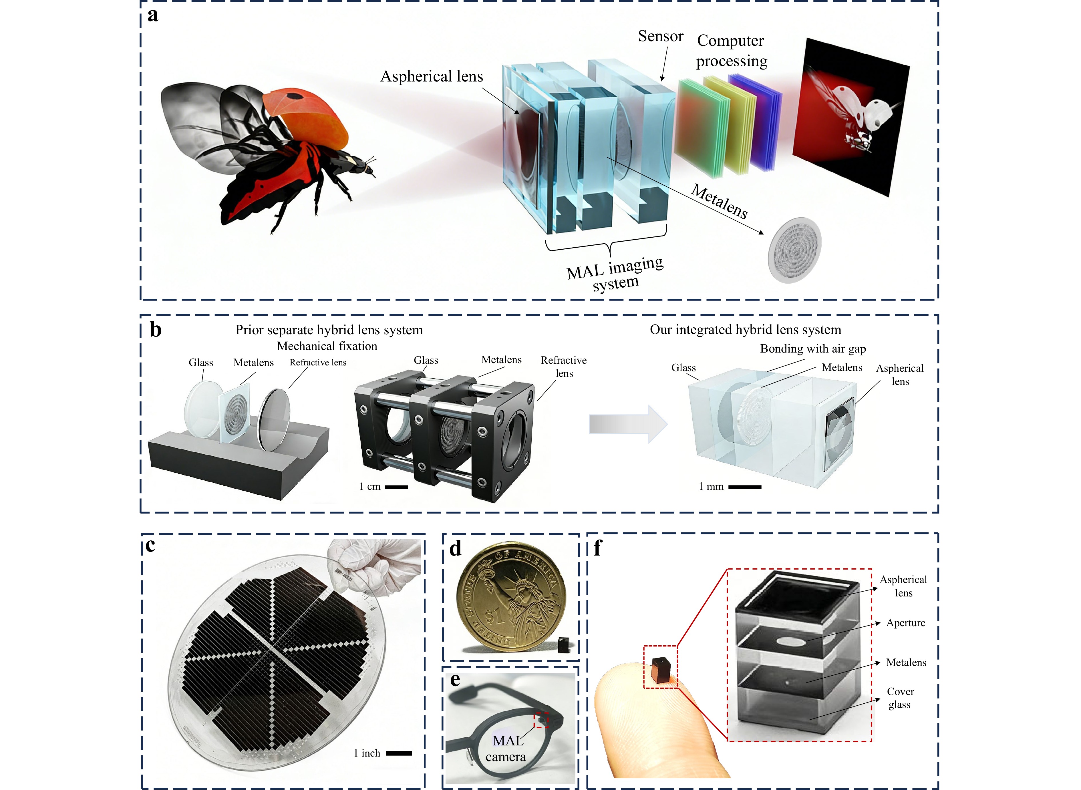
Fig. 1 Schematic and demonstration of the MAL. a Illustration of the MAL computational imaging system, comprising a hybrid optical module and a computational processing module. The optical module captures and encodes the near-infrared light field via the meta-aspheric lens, whereas the computational module reconstructs high-fidelity images through algorithmic processing. b Comparison between separated and integrated hybrid lens systems. The integrated design eliminates auxiliary mechanical clamping and complex alignment requirements, allowing volume compression to the cubic millimetre scale while maintaining optical performance and structural robustness. c MAL mass-produced on an 8-inch wafer, demonstrating the scalability of the wafer-level fabrication process, through which thousands of devices can be manufactured simultaneously. d Photograph of the fabricated MAL, demonstrating its compact form factor, which is significantly smaller than that of a US one-dollar coin, underscoring its suitability for integration into space-constrained mobile platforms. e Demonstration of MAL integration into AR glasses, showing seamless deployment without compromising aesthetic design or user experience, thereby validating its practical applicability in wearable devices. f Enlarged view of the fabricated MAL shows that the integrated design has completely solidified the optical system that combines aspherical lenses and metalens. The entire hybrid lens is substantially smaller than a human finger.
Our wafer-scale manufacturing process enables high fabrication precision. To better illustrate the fabrication process, we fabricated a small-area wafer featuring a 6 × 5 device array to clearly depict the intermediate products of wafer-level optical manufacturing. The metalenses fabricated on the wafer are shown in Fig. 2a. Fig. 2b shows the assembled state after the alignment and bonding of the metalens array wafer and the WLO aspherical lens. Scanning electron microscopy (SEM) images of the individually fabricated metalenses are shown in Fig. 2c, and a partially enlarged view is shown in Fig. 2d. Fig. 2e shows a side-view SEM image of the metallic nanocylinders with heights close to the designed value of 550 nm. Notably, the result of manufacturing lateral linewidth of the nanocylinders aligned well with the design, as shown in Fig. 2f. For WLO aspherical lens fabrication, we employed techniques such as direct laser writing and nanoimprint lithography. Fig. 2g compares the designed and measured heights of the aspherical lens. The average absolute error (MAE) within the radial coordinate R ranging from 0.5 to 0.6 mm is only 280 nm. The high-precision fabrication of aspherical lenses further demonstrated our wafer-level optical manufacturing capability for mass-producing MAL.
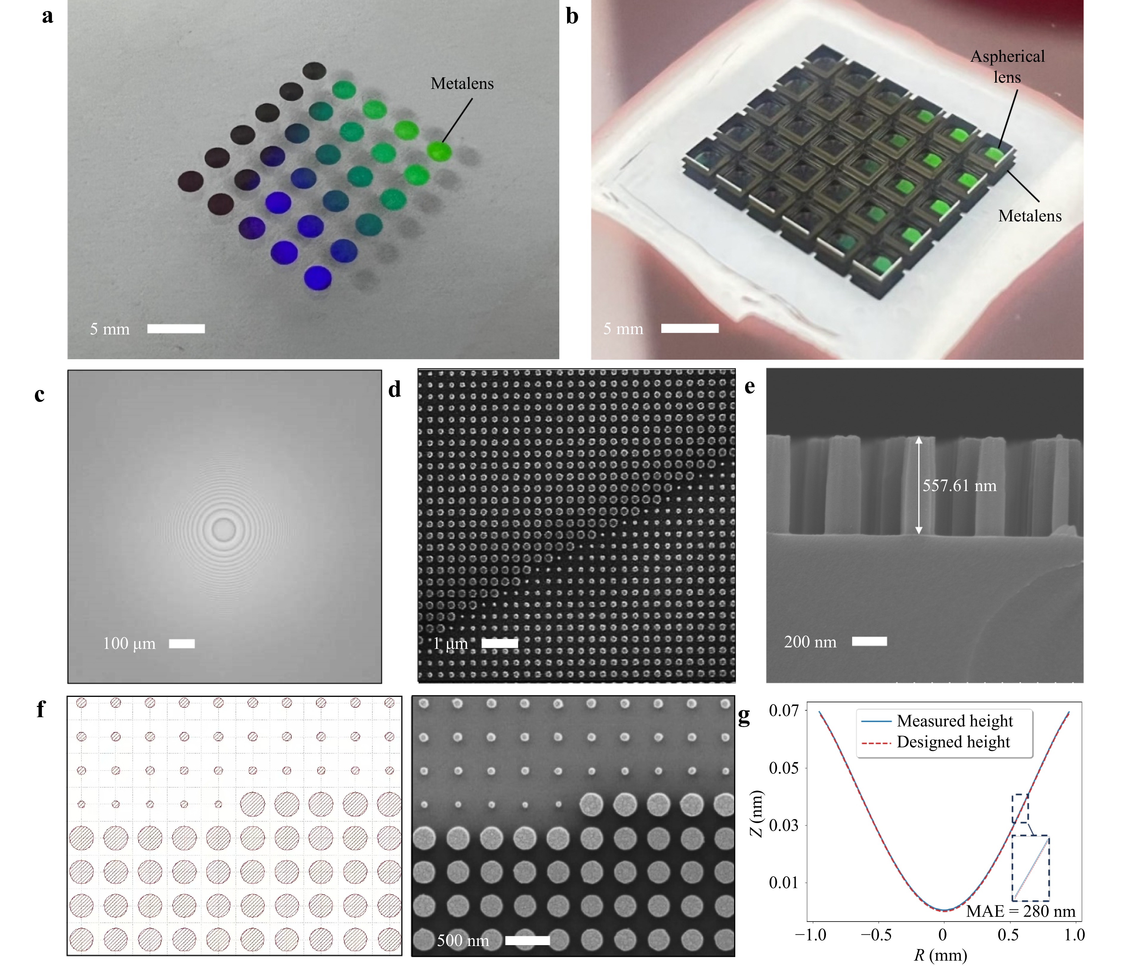
Fig. 2 Morphology characterization of the Manufactured metalens and aspherical lens. a Small-area fabricated wafer with 6 × 5 metalens arrays b Bonded MALs after wafer-level integration, captured using mobile photography. c SEM image of an individual metalens on the wafer. d Enlarged SEM image of the metalens, showing α-Si nanopillars with diameters ranging from 80–290 nm, arranged in a square lattice with a 400 nm period. e Side-view SEM image of the nanopillars, with a height close to the designed value of 550 nm. f Comparison between the metalens layout and the fabricated structure, demonstrating excellent fidelity between the designed pattern and the manufactured nanostructures, with high accuracy across the entire aperture. g Comparison of the measured and simulated aspherical lens profiles. The average absolute error (MAE) between the measured and designed values at R = 0.5−0.6 mm is 280 nm.
-
The performance of the MAL was analysed using ANSYS Zemax Optic Studio. To obtain high-quality images, it is essential to obtain high-contrast and high-resolution images across the entire FOV, as shown in Fig. 3a. Fig. 3b shows a tangential ray trace of the MAL at 0 °–50.75°. The designed MTF diagrams of the sagittal and tangential beams are shown in Fig. 3c. The MAL demonstrated a high MTF, exceeding 0.5 at 38 lp/mm and 0.31 at 50 lp/mm under the maximum field of view, meeting the diffraction sampling limit for a 640 × 480 sensor array with 3 µm pixels. We provide the designed MTF diagrams of the sagittal and tangential beams at 12 angles within a 0°–50.75° FOV in Note S1 of the Supplementary Materials.
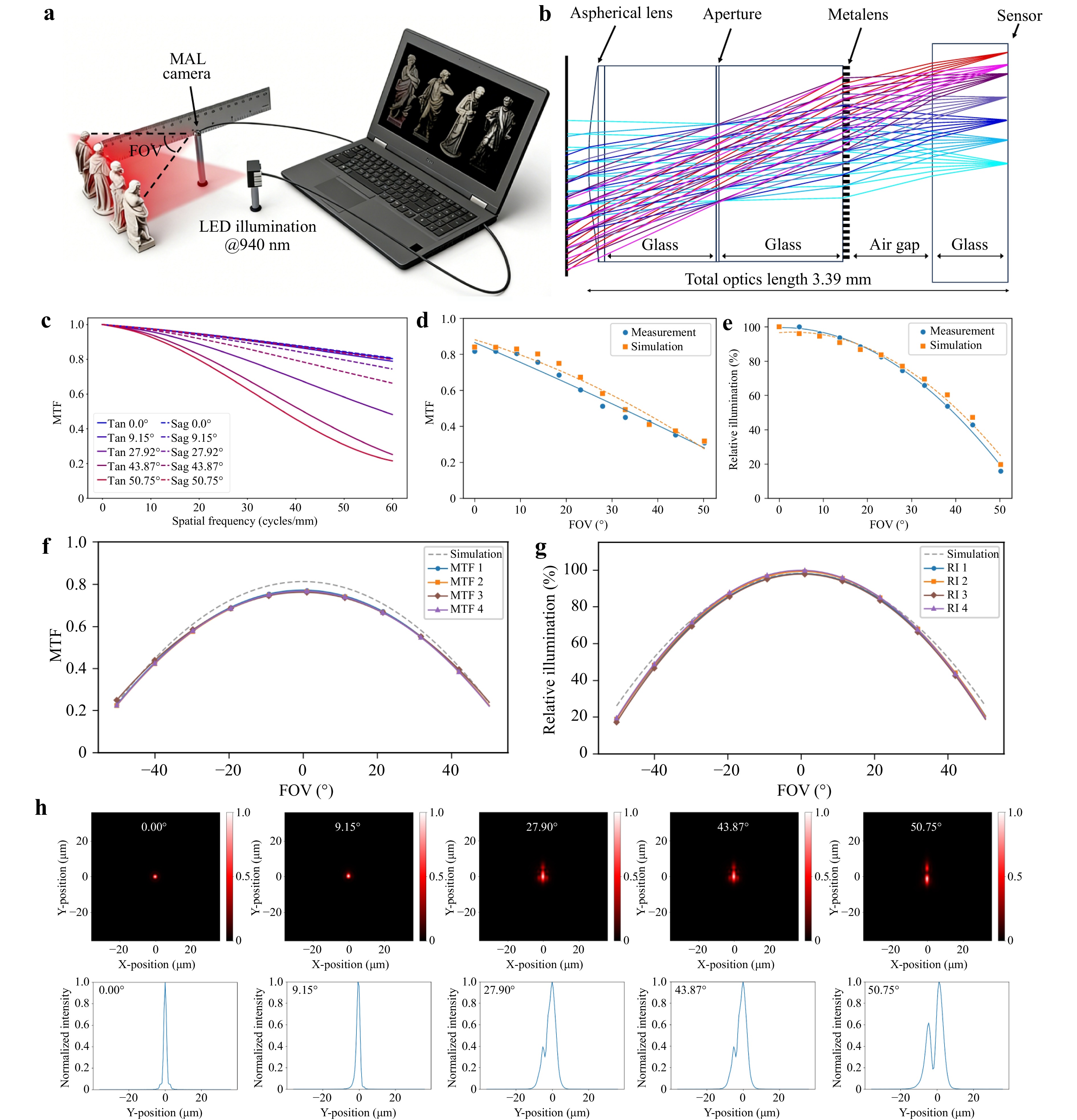
Fig. 3 Design and results analysis of the MAL. a Schematic of the wide-FOV MAL imaging system. b Ray tracing at different FOVs through the MAL, illustrating the optical path from object space through the integrated hybrid lens to the sensor plane, achieving a 101.5° diagonal FOV within a 3.39 mm total track length. c Designed MTF curves including sagittal and tangential components at different FOVs, showing diffraction-limited performance with values exceeding 0.31 at 50 lp/mm across the entire field. d Difference between the measured and simulated MTF of the MAL at 50 lp/mm. e Difference between the measured and simulated relative illumination of the MAL. f Full field-of-view MTF measurement values of MAL at four random positions on the wafer. g Full field-of-view relative illumination measurement values of MAL at four random positions on the wafer. h Point spread function (PSF) and corresponding cross-sectional intensity distributions at five different FOVs. The PSF intensity distributions at 12 angles within the 0°−50.75° FOV are provided in note S1 of the Supplementary Materials.
These results indicate the ability of the MAL to provide the necessary high contrast for high-quality imaging. Detailed analyses of the distortion, field curvature, spot diagrams, optical path difference, and grid distortion are discussed in Note S1 of the Supplementary Materials. Notably, the proposed MAL adopts an integrated design that considers the manufacturing process capabilities and structural integration by combining the actual dispersion model of the metalens to calculate the imaging performance of the hybrid lens. Fig. 3d, e show the measured MTF at 50 lp/mm and the relative illumination (RI) of the MAL, respectively, demonstrating that the MTF and illumination measured in the real experiment agreed well with the designs. This agreement can be attributed to our integrated design, which considers the material dispersion model and high-precision wafer-level manufacturing technology. By contrast, significant discrepancies often occur in conventional hybrid lens system designs owing to inherent design and processing errors21. The relevant data are presented in Supplementary Material S1. To demonstrate the robustness and reproducibility of this wafer-level manufacturing process, we measured MTF and RI values for four MALs at random positions on the wafer using ImageMaster® HR 2, as shown in the Fig. 3f, g. This proves that our wafer-level manufacturing of MALs has high consistency in performance.
To further characterise the imaging performance of the designed MAL, its focusing performance was demonstrated using the designed PSF intensity distribution at 940 nm. As depicted in Fig. 3h, the PSF of MAL displays relatively uniform peak intensities at 0°, 9.15°, 27.90°, 43.87°, and 50.75°. Furthermore, we show the PSF intensity distribution at 12 angles within a 0°–51.51° FOV in Note S1 in the Supplementary Materials. This demonstrates that our MAL maintains a relatively stable focusing performance across the entire FOV, although slight aberrations inevitably emerge near the field edge, degrading the captured images. The PSF enables the accurate simulation of raw images of the target light field at different FOVs after propagation through the MAL, supported by the strong agreement between the experimentally measured and designed MTF and relative illumination. Additionally, the designed PSF can be used as a blur prior for digital imaging, enabling aberration correction across the entire FOV or pixel super-resolution via computational imaging to enhance image quality.
-
We experimentally tested the MAL imaging resolution using a USAF resolution test chart and demonstrated its imaging performance, as shown in Fig. 4a. To objectively substantiate the achievable spatial resolution, we analysed each element of the USAF 1951 target in Groups -1 and 0 using only two scalar metrics: the Michelson contrast and contrast-to-noise ratio (CNR). For each element, a centred region of interest (ROI) was extracted and averaged orthogonally to the stripe orientation to obtain a one-dimensional intensity profile. The peak and valley intensities were robustly estimated as the means of the local maxima and minima, respectively, whereas the local noise was quantified from the standard deviations within the peak and valley neighbourhoods. An element was declared resolvable if Michelson was ≥ 0.10 and CNR was ≥ 2.0, which are thresholds consistent with widely used visibility limits for low-contrast periodic patterns. Elements with a CNR ≥ 3 were additionally labelled “robust”. Under these criteria, the measured ROI in Group −1 exhibited a Michelson contrast of 0.9141 and a CNR of 3.1838, whereas the ROI in Group 0 exhibited a Michelson contrast of 0.8935 and a CNR of 3.1723. These values are well above the adopted resolvability thresholds, indicating large luminance modulation and low relative noise.
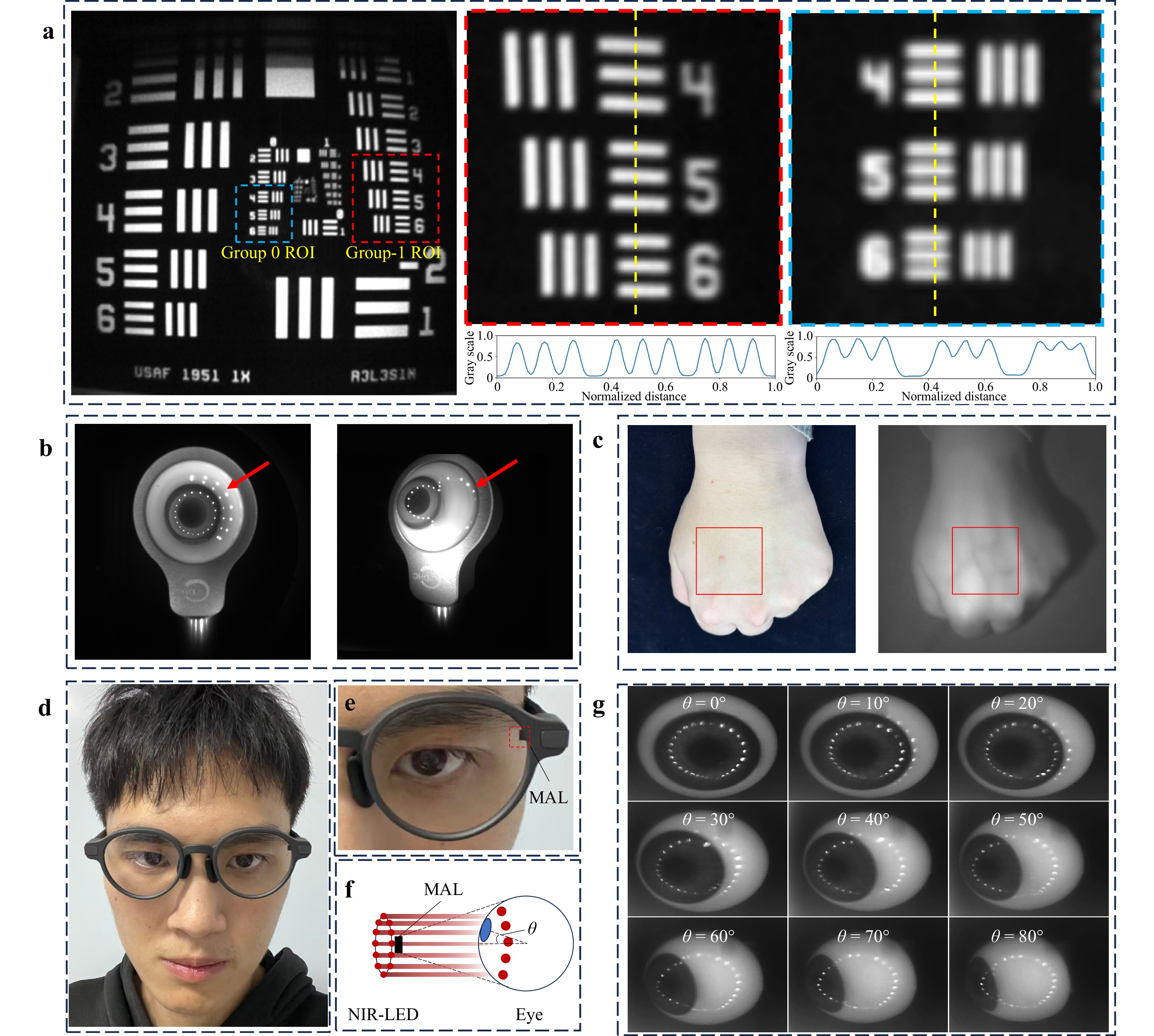
Fig. 4 Imaging experiments using the MAL. a Imaging results and quantitative analysis at different contrast levels using a resolution target. The left panel shows the raw captured image and the right panel displays magnified regions from Groups -1 and 0. Resolution analysis revealed that Group −1 elements achieved a Michelson contrast of 0.914 and a CNR of 3.1838, whereas Group 0 elements achieved 0.894 Michelson contrast and 3.1723 CNR, both exceeding the resolvability thresholds (Michelson ≥ 0.10, CNR ≥ 2.0) and robust detection criteria (CNR ≥ 3). b Photograph of an eye model captured by the MAL at different angles, clearly showing distinct dot pattern distributions reflected as the eyeball rotates. The images demonstrate the ability of the MAL to resolve subtle retinal features across a defined angular range, supporting its potential for high-precision eye-tracking applications. c Comparison of hand images captured by a visible light camera and the MAL camera, demonstrating the ability of the MAL to capture subcutaneous blood vessels. d A conceptual illustration of eye-tracking implementation using MAL on AR glasses, and e providing the corresponding magnified view. f A schematic diagram of the close-range eye imaging test setup, featuring an annular arrangement of near-infrared LEDs for illumination, with the MAL employed to capture eye models at various rotation angles along with the reflected infrared light spots. g Imaging results of the eye model at various orientations, demonstrating clear capture of ocular contours and reflected light spots across different angles, thereby enabling the identification of current eye movement states.
Our MAL demonstrates excellent near-infrared imaging performance because it has a 30 nm design bandwidth, which enables excellent imaging results in areas such as eye tracking and vein imaging. As an example, we captured images of an eye model from different angles to demonstrate its potential in eye tracking applications, as illustrated in Fig. 4b. The results showed that the different ocular structures could be clearly distinguished across various imaging angles. Additionally, we evaluated the ability of the MAL to support subcutaneous tissue imaging by comparing hand vascular images acquired independently using a visible-light camera and the MAL camera, as shown in Fig. 4c. The MAL camera provides clear visualisation of the dorsal hand veins, which cannot be achieved by conventional visible-light imaging. As an important application, we have made a conceptual demonstration of the application of eye tracking on AR glasses, as shown in Fig. 4d, e. The volume advantage of the MAL enables seamless deployment on AR glasses, and the provided large FOV imaging performance allows capturing the complete eye contour, iris features, and eye movement status at a close range. We conducted tests on close-range eye imaging to simulate the application of the MAL in AR glasses using the experimental setup illustrated in Fig. 4f. A near-infrared LED strip served as the illumination source, whereas the MAL captured the ocular contours and reflected light spots. Fig. 4e shows the MAL imaging performance of the eye models at different rotation angles under close-range conditions. The ocular contours and corneal reflection spots were clearly discernible across all tested angles, with their varying positions enabling accurate identification of gaze direction and determination of current eye movement states. These results demonstrate the substantial application potential of MAL in next-generation intelligent display devices. This potential stems from the extreme sensitivity of eyewear-type AR and AI devices to the form factors and dimensions, where the module size of the eye-tracking optical solution represents a critical parameter. Furthermore, an expanded imaging field of view (FOV) ensures the acquisition of broader visual information under close-range conditions, which aligns precisely with the inherent advantages of the MAL. Such MAL can also be applied to tasks such as facial, iris, and fingerprint recognition because these applications rely mainly on monochromatic illumination from near-infrared light. Moreover, we demonstrated computational super-resolution imaging by combining MAL with a deep learning model. Specific implementation details can be found in the Supplementary Materials S3. In subsequent studies, we shall explore the design of larger bandwidths to support applications such as functional imaging, blood-oxygen imaging, and night-vision imaging, which are required for autonomous driving. This can be achieved through the application of our proposed metalens design model, which features practical dispersion. This functionality could be integrated into AR glasses for future surgical navigation applications.
-
A wafer-level MAL represents a significant advancement in compact optical system design, resolving the long-standing trade-offs between miniaturisation, optical performance, and high-volume manufacturability. While previous studies have combined refractive and metasurface optics, they largely treated the metalens as an add-on component to correct aberrations or reduce the size within a conventional optical design framework. In contrast, we introduce a codesign strategy that fully integrates the metasurface and aspherical lens from the beginning as a single optical entity that is enabled by our new concept of “design for hybrid manufacturability”, where optical design proactively incorporates key fabrication constraints—such as bonding interfaces, material dispersion matching, and wafer-scale processes—rather than treating manufacturing as a post-design consideration. Consequently, the metasurface and aspherical components are not simply stacked; they are jointly optimised and bonded at the wafer level without the need for alignment or mechanical support. This approach moves beyond component-level innovation to introduce a system-level methodology that unifies design and mass manufacturing, thereby closing the gap between laboratory demonstrations and scalable commercial applications.
The performance of our MAL was validated across multiple imaging modalities, including direct near-infrared (NIR) imaging for eye tracking and blood vessel visualisation. This comprehensive demonstration confirmed the versatility and effectiveness of the MAL for both hardware-limited and computation-enhanced imaging scenarios. The synergy between advanced optics and computation is particularly important for NIR applications, in which both resolution and low noise are critical for applications such as biometrics and medical diagnostics.
In the future, we shall optimise wafer-level fabrication to improve the yield and reduce costs, expand integration with advanced computational imaging for challenging conditions, and develop application-specific MAL designs. Moreover, adopting a fully differentiable end-to-end optimisation of manufacturability and downstream optical tasks, as well as computational reconstruction methods such as the neural lithography framework, could be another exciting next step30,31. Progress in these directions will solidify the MAL technology as a cornerstone for the next generation of compact, high-performance imaging systems.
By integrating metalenses, aspherical lenses, wafer-level manufacturing, and both direct and computational imaging into a single platform, this study advances the development of compact optical system design. The MAL platform shows strong potential for applications in mobile devices, AR/VR systems, medical imaging, navigation, and other industrial applications.
-
Our MAL system is based on a monolithic wafer-level hybrid architecture that integrates an aspherical lens and a metalens. This system achieves high optical performance and alignment robustness, and is compatible with mass production. The design was jointly optimised in the Zemax Optic Studio for both imaging performance and manufacturability. System Architecture and Integration Strategy: MAL employs aspheric and metallic surfaces as primary functional interfaces bonded by a D263T glass substrate. The substrate thickness was treated as a design variable during optimisation to balance the optical performance, compactness, and process constraints. For robust integration, the rear glass surface featured an enlarged aperture, and the reserved edge was engineered for structural bonding. A controlled air gap above the metasurface preserved the integrity of the nanostructures during the assembly. Aspherical lens surface modelling: The aspherical lens profile is described as follows:
$$ {\textit z}(r) = \frac{c{r}^{2}}{1+\sqrt{1-(1+k){c}^{2}{r}^{2}}}+\sum \nolimits_{n=1}^{m}{a}_{2n}{r}^{2n} $$ (1) where z(r) is the surface sag at the radial coordinate r, c = 1/R is the curvature, k is the conic constant, and $ {a}_{2n} $ is the even-order aspheric coefficient. The surface profile was optimised for minimal aberration to ensure process compatibility (Table S1, Supplementary Materials).
-
The metalens phase distribution is defined as follows:
$$ \varphi \left(x,y\right) = M \sum \nolimits_{i=1}^{n}{a}_{n}{\left(\frac{\rho }{R}\right)}^{2i} $$ (2) where $ \rho $ is the radial coordinate, R is the normalised metalens radius, and $ {a}_{n} $ are polynomial coefficients chosen to minimise the focal spot size across the required FOV. The phase profile was empirically controlled using 10 polynomial terms for accurate wavefront shaping. Each phase value is implemented with a circular α-Si nanopillar meta-atom, which is simulated via Lumerical FDTD and arranged in a square lattice (400 nm period). The diameter of the nanopillars ranged from 80 to 290 nm, with a fixed height of 550 nm, enabling continuous phase coverage (0−2π) at high transmittance for the design wavelength of 940 nm (see Fig S2h and Fig S2i, Supplementary Materials). For each position (x,y), the optimal unit cell is assigned from a precomputed database by minimising the combined phase and transmission errors:
$$ \begin{split}R\left(x,y\right)=\;&\underset{R}{\text{argmin}} (| {\varphi }_{meta}\left(x,y,{\lambda }_{0}\right)-\\&\varphi \left(x,y\right)| +\left| {T}_{meta}\left(x,y,{\lambda }_{0}\right)-1\right| )\end{split} $$ (3) where $ {\varphi }_{meta} $ and $ {T}_{meta} $ are the phase and transmission, respectively, for a unit cell at the design wavelength.
-
To ensure that the simulated performance is translated to fabrication, the idealised meta-atom dispersion model is replaced by the experimentally measured dispersion curve of the actual α-Si material. The forward model for local phase modulation then becomes
$$ \varphi \left(x,y,\lambda ,\theta \right)=f(R\left(x,y\right),\lambda ,\theta ) $$ (4) where $ f $ is a bespoke operator that maps the structural distribution, wavelength λ, and incident angle θ to the corresponding phase. This model enables a rigorous and realistic evaluation of the system’s MTF, relative illumination, and broadband/off-axis behaviour, supporting co-optimisation for process compatibility and yield (see Fig S2b and Fig S2c, Supplementary Materials). By incorporating both process-aware geometric constraints and experimentally validated optical models, our design ensures that MAL can support high imaging performance and is directly compatible with wafer-scale manufacturing and assembly.
-
As illustrated in Fig. 5, the fabrication of the MAL involves several main stages: (1) wafer-level fabrication of the metalens, (2) wafer-level fabrication of the aspherical lens, (3) stacking and bonding of the two elements with a micrometre-level alignment for dicing, and (4) integration of the diced MAL with the cover glass and imaging sensors via an engineered air gap.
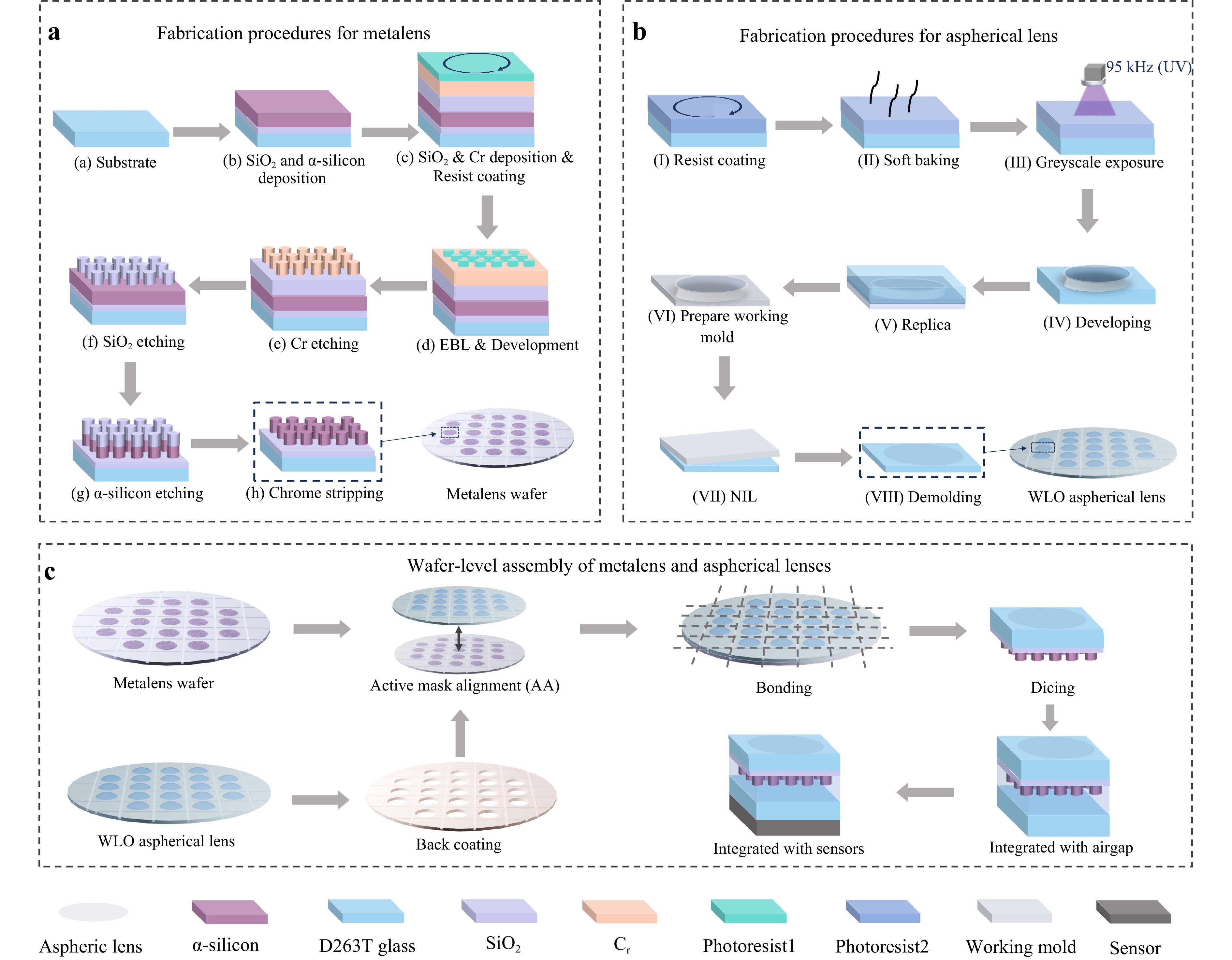
Fig. 5 Fabrication process of the MAL. a Wafer-level fabrication of the metalens via electron beam lithography and inductively coupled plasma (ICP) etching. b Wafer-level fabrication of the aspherical lens through laser direct writing and nanoimprint lithography, producing high-precision curved surfaces in a UV-curable polymer. c The backside-coated WLO aspherical lens wafer is aligned and bonded to the metalens wafer, then diced, bonded to the final glass element with air gap, and ultimately integrated onto the sensor.
1. Metalens Fabrication: As shown in Fig. 5a, the process began with a 0.5 mm thick D263T Eco glass substrate. A 10 nm SiO2 adhesion layer is first deposited by plasma-enhanced chemical vapour deposition (PECVD), followed by 550 nm of α-silicon. Next, a 30 nm Cr hard mask is sputtered onto the α-silicon surface, and another 30 nm SiO2 layer is deposited to protect the mask. The designed nanostructure was patterned onto a wafer using electron-beam lithography (EBL, Raith EBPG 5200) with a negative-tone photoresist (maN-2403). After exposure, the resist is developed (ma-D 525, 35s), and the pattern is sequentially transferred: first into the SiO2 (by ICP etching, Oxford PlasmaPro 100 Cobra300), then into the Cr (ICP etching, Oxford PlasmaPro 100/1), and finally into the underlying α-silicon layer (ICP etching, Oxford PlasmaPro 100 Cobra300). The remaining Cr mask was removed using a wet chrome etchant to complete the metalens nanostructure.
2. Aspherical Lens Fabrication: In parallel, a nonspherical (aspherical) lens structure was fabricated on a separate wafer using direct laser writing and nanoimprint lithography (NIL). The aspherical lens was formed in a photoresist or UV-curable polymer, as shown in Fig. 5b. After wafer coating and soft baking, the lens shape was defined by UV exposure (at 95 kHz), followed by resist development, transfer onto a working mould, and nanoimprint lithography to obtain the final aspheric profile.
3. Wafer-level assembly of the metalens and spherical lenses: After both optical elements were fabricated, wafer-level bonding was performed, as shown in Fig. 5c. First, the back of the aspherical lens is coated with chromium. Then, using active mask alignment (AA) technology, the WLO aspherical lens and metalens wafer were aligned with micrometre-level precision to ensure precise matching of the positions between the two optical components. The bonded wafers were diced and integrated with D263T glass, retaining the air gap. Finally, they were installed on the imaging sensor to complete the device assembly.
Using this technology, we achieved the batch manufacturing of hybrid lenses on wafers. Notably, our process involves presetting mark points on the wafer and using a mask alignment for bonding. For each MAL on the wafer, the metalens was primarily connected at the edge and had an air gap at its centre. This design ensures the stability of the structure and considers the structural stability of the metalens nanocylinder while preventing damage to the original meta cell during the manufacturing process.
In summary, the above process supports the wafer-level monolithic integration of aspheric and metasurface optics, enabling high-yield mass production with minimal alignment errors without requiring post-fabrication mechanical fixtures. Although we employed EBL for wafer-scale metalens patterning in this study32, other existing processing methods can be used to improve the production efficiency of metalenses for large-scale manufacturing33–36. In subsequent work, we shall consider improving the manufacturing processes at the wafer level by comprehensively considering multiple factors, such as production accuracy, production efficiency, and time cost, to achieve a more efficient wafer-level manufacturing of microimaging lenses.
-
This work was funded by the National Key R&D Program of China (2022YFB4602600 and 2024YFF05603), National Natural Science Foundation of China (Grant Nos. 52425508, 52221001, and 62271414), and the Key R&D Program of Hunan Province (2025JK2009). We thank Goertek Omnilights NanoOptics Co., Ltd. (Shanghai, China) for the financial and technical support. We are grateful to Mr. Junyan Zhu and Mr. Xibian Wei for helpful discussions, and Dr. Keqi Ma for technical assistance. We also thank Mr. Xiangbiao Liu of the Wuhan Binary Technology for supporting the numerical simulations. We are grateful to Dr. Yuan Chen for his leadership in manufacturing. We also acknowledge Even Realities for providing the AR glasses featured in the figures of this manuscript.
Ultracompact Wide-FOV near-infrared camera with a wafer-level manufactured meta-aspheric lens
- Light: Advanced Manufacturing , Article number: 45 (2026)
- Received: 03 March 2026
- Revised: 18 March 2026
- Accepted: 18 March 2026 Published online: 22 April 2026
doi: https://doi.org/10.37188/lam.2026.045
Abstract: Overcoming the trade-off between a wide field of view (FOV) and compactness remains a central challenge for integrating near-infrared (NIR) imaging into smartphones and AR glasses. Existing refractive NIR optics cannot simultaneously support ultrawide angles above 100° and ultrathin total track lengths (TTL) below 5 mm, fundamentally limiting their integration into portable devices. Herein, we present a wafer-level-manufactured meta-aspheric lens (MAL) that simultaneously achieves a 101.5° FOV, 3.39 mm TTL, and F/1.64 aperture within a compact volume of 0.02 cm3. Unlike previous hybrid systems that rely on separate refractive and diffractive components, the proposed MAL introduces a fully integrated architecture that provides a compact form factor. This integration also simplifies fabrication by enabling high-throughput production via micrometre-level precision alignment and bonding on a single wafer, which requires only one dicing step and no additional mechanical fixtures. Furthermore, the design process incorporates manufacturability and enables metalens dispersion modelling, ensuring that the experimental performance matches simulation results. We validated the MAL method using both direct and computational imaging experiments. Despite its small form factor, our scalable MAL demonstrated strong NIR imaging performance in eye tracking, blood vessel imaging, and computational pixel super-resolution tasks. This scalable MAL technology establishes a new benchmark for high-performance miniaturised NIR imaging, and opens the door for next-generation smartphones and AR optical systems.
Research Summary
Meta-aspheric lens: Wafer-scale manufactured enables ultracompact infrared cameras
A camera lens combining refractive and metasurface optics achieves 101.5° field of view in just 3.39 mm thickness, enabling high-performance near-infrared imaging for smartphones and AR glasses. Chuirong Chi from Hunan University and colleagues developed a meta-aspheric lens manufactured entirely at the wafer level, eliminating bulky mechanical supports and complex alignment steps. The integrated design compresses volume to 0.02 cm³ while maintaining sharp imaging quality validated through eye-tracking and blood vessel visualization experiments. This scalable manufacturing approach bridges laboratory demonstrations and mass production for next-generation mobile devices.
Rights and permissions
Open Access This article is licensed under a Creative Commons Attribution 4.0 International License, which permits use, sharing, adaptation, distribution and reproduction in any medium or format, as long as you give appropriate credit to the original author(s) and the source, provide a link to the Creative Commons license, and indicate if changes were made. The images or other third party material in this article are included in the article′s Creative Commons license, unless indicated otherwise in a credit line to the material. If material is not included in the article′s Creative Commons license and your intended use is not permitted by statutory regulation or exceeds the permitted use, you will need to obtain permission directly from the copyright holder. To view a copy of this license, visit http://creativecommons.org/licenses/by/4.0/.

 DownLoad: