


-
With the advancement of conventional photolithography, feature sizes of integrated circuit devices have continuously shrunk from the micrometre scale to the submicrometre and even nanometer scale1,2. However, the resolution of photolithography is gradually approaching its theoretical limit3,4. Consequently, mask costs, manufacturing complexity, and the demand for extremely high alignment accuracies have increased significantly5. Simultaneously, emerging nanophotonic components, such as ultraviolet metalenses and metasurfaces, demand extremely high pattern density, subwavelength feature control, and flexible fabrication capability6–9. Maskless projection lithography technology based on spatial light modulators (SLMs) has emerged as a potential solution to address the increasing cost of conventional photolithography10–12. It has been extensively investigated as the next-generation lithography technology. For instance, utilising a digital micromirror device (DMD) or a liquid crystal-on-silicon spatial light modulator (LCOS-SLM) to generate digital masks not only reduces the cost of mask fabrication but also enhances lithographic flexibility and production efficiency10,13. Although it cannot completely replace the mainstream lithography technology used currently, it simplifies the intricate process of conventional photolithography, thus offering cost-effectiveness, high efficiency, and flexibility. Furthermore, maskless projection lithography can expand the wide-band range of light sources, including continuous, pulsed, and ultrafast femtosecond visible and ultraviolet lasers11,12. This indicates its strong technical extensibility and process compatibility, which renders it readily applicable to highly customised photonic and electronic devices10,12,13.
To enhance the ultimate resolution of DMD projection lithography, recent efforts typically involve using short wavelengths (193, 248, or 365 nm) coherent light sources14–16, incorporating high-density small pixel elements (5.4 μm) in DMD chips17–19, and reducing the reduction ratio of the projection lens with a high numerical aperture (NA)12,20. However, owing to the limited size of individual pixel elements on the DMD chip, which is approximately 10 μm17, conventional maskless lithography based on DMD typically adopts a reduction ratio of ~1/5× to ~1/10×, thus resulting in an ultimate resolution at the scale of ~1 μm15. As the reduction ratio of the projection lens decreases, for example, to 1/100×–1/300×10, the spacing between adjacent micromirror pixel elements on the DMD chip’s focal plane becomes less than 100 nm, which is smaller than the optical diffraction limit (i.e. 0.61 λ/NA)10–12. However, the size of a single pixel element’s image cannot exceed the limit, which is approximately 200 nm10. Consequently, adjacent pixels or multiple elements will inevitably cause image overlap, thereby significantly reducing the lithographic resolution18–20. Consequently, neither finer linewidth features nor increased density of fine lines per unit area can be achieved, thereby limiting the information capacity and functionality of individual chips.
Phase-shifting mask (PSM) technology is typically employed to enhance the resolution of lithography systems21–24. It introduces a π phase difference in adjacent transparent regions, thus creating interference cancellation at the edges of an image to increase contrast and thus improve imaging resolution21,24,25. Based on this principle, if PSM technology is applied to maskless projection lithography, it can effectively enhance lithography resolution. However, conventional PSM fabrication requires the deposition of a phase-shifting layer measuring approximately one wavelength and a specific thickness in each designed mask-pattern region4,21,24. This is impractical for projection lithography systems without physical mask templates, where depositing a phase-shifting medium layer on programmable digital mask micromirror elements is not feasible26.
In this study, we propose a method to enhance the resolution of optical projection lithography using a phase-modulated digital mask, termed digital phase-shifting mask projection lithography (PSM-DPL). Prior to generating digital masks using DMDs or an LCOS-SLM, direct phase modulation of the imaging beam is performed using a pair of cascaded SLMs. This is achieved through pixelated modulation of the illumination light’s phase parameters during optical exposure using a computer-controlled SLM. Meanwhile, the interference state between the intensities of adjacent pattern elements on the image plane is altered by introducing a phase difference (or odd multiples) in the adjacent micromirror pixel areas. This causes interference cancellation in the projection of adjacent elements, thus reducing the intensity of dark areas in the light-field distribution and enhancing the intensity of bright areas. Consequently, the imaging contrast and resolution of projection lithography are improved.
-
The PSM-DPL system is illustrated in Fig. 1a. The light source is a femtosecond pulse laser with a central wavelength of 517 nm, a repetition rate of 10 MHz, and a pulse width of ~240 fs. The collimated and uniformised flat-top optical field is modulated by the digital mask, thus resulting in pixel-controlled patterned optical-field information with independent amplitudes and phases. Subsequently, this patterned target optical field is projected onto the photoresist and rendered smaller using the projection lens system, which includes a tube lens (f = 200 mm), an NA of 1.40, and a 100× oil-immersion objective lens, thereby achieving precise exposure of the target pattern. Additionally, the system includes a real-time monitoring unit to ensure the correct transmission of optical-field information during the exposure process. A detailed description of the PSM-DPL system is provided in Supplementary Fig. S1.
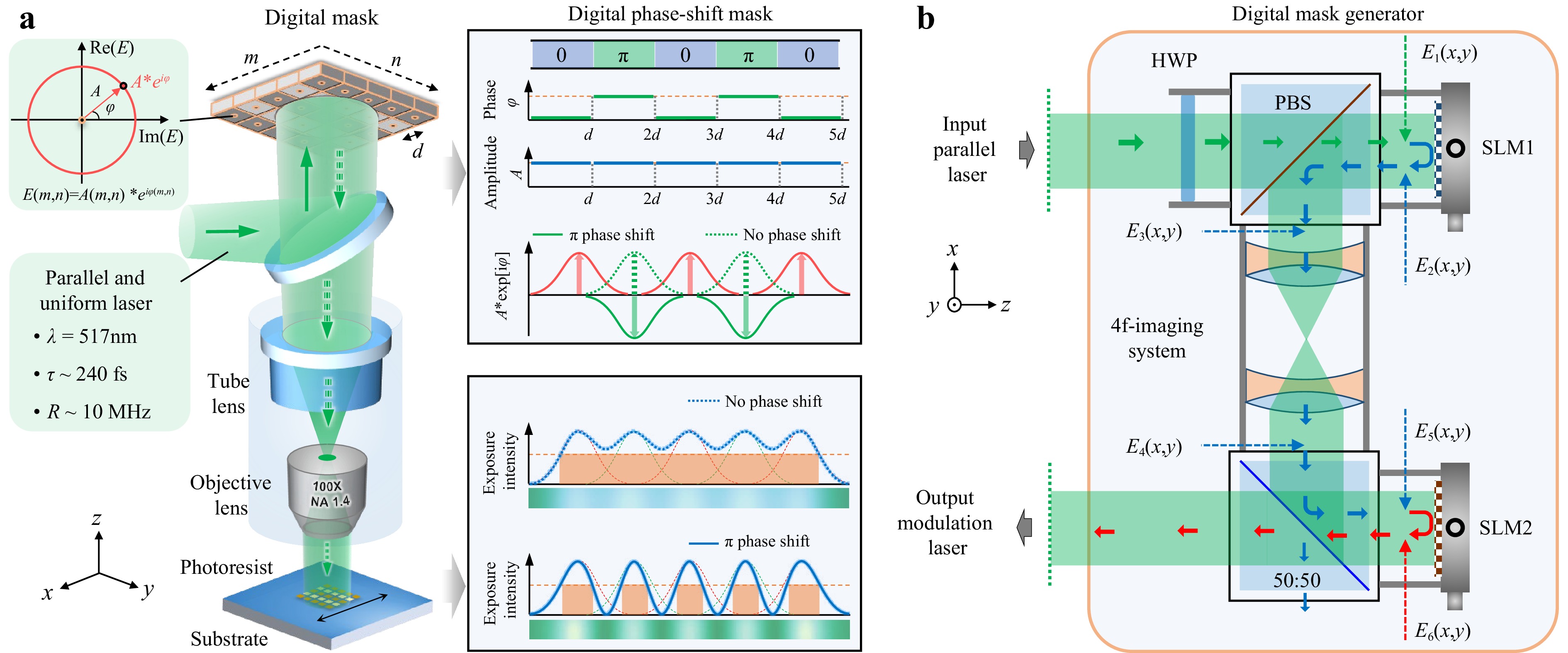
Fig. 1 Scheme of the experimental system and method for digital phase-shift mask projection lithography. a A Typical digital mask projection lithography system, including the light source, digital mask, projection optical components (tube lens and objective lens), photoresist, and substrate. The digital mask shown in the upper inset generates amplitude- and phase-modulated patterned light fields, such as dense wire grid patterns. The inset below shows a comparison of exposure results with and without a PSM. The adjacent line patterns, which introduce π phase shifts, have resolvable spacing and higher pitch resolution. b Optical path subsystem of digital mask generates a patterned PSM through amplitude- and phase-type LCOS-SLM cascade modulation of light field. SLM1 and SLM2 are amplitude- and phase-type SLMs, respectively.
The programmable digital mask can generate arbitrary target patterns, with dense line patterns as an example. When the designed line-to-line spacing is excessively small, the optical fields of adjacent lines overlap at the focal plane of the objective lens and become indistinguishable, as shown in the inset of Fig. 1a. However, the programmable PSM introduces a phase difference of π between adjacent patterns, thus altering the interference overlap status of the original adjacent patterns27. This changes them from an interference phase overlap to an interference phase cancellation, thereby creating a zero-field region in the middle of adjacent line patterns. Consequently, the brightness and darkness of the optical field change significantly, thus enhancing the contrast of the patterns and improving the resolution under identical exposure conditions.
-
The amplitude and phase information of the target pattern are independently modulated with high flexibility through a cascaded configuration of amplitude- and phase-type LCOS-SLMs, as shown in Fig. 1b. Collimated and linearly polarised light passes through a half-wave plate and a polarisation beam splitter before entering the amplitude-type LCOS-SLM, where it undergoes amplitude modulation. The half-wave plate’s angle is adjusted to ensure maximum utilisation of the incident light. The polarisation beam splitter serves as an input/output polariser and, in conjunction with the amplitude-type LCOS-SLM, modulates the polarisation state of the reflected light, thereby changing the output intensity. This results in amplitude modulation. Subsequently, the optical field containing the amplitude information of the target pattern is directed into a 4F pixel-matching system comprising two identical tube lenses with a 1:1 magnification ratio and is then incident on the phase-type LCOS-SLM (Fig. 1b). This system accomplishes the composite modulation of the optical-field information, including both amplitude and phase. The amplitude- and phase-type LCOS-SLMs have the same parameters, such as image plane size, resolution (1,080 × 1,920 pixels), and pixel size (8 μm × 8 μm) (see Table S1). The 1:1 pixel-matching system (Fig. S2 and Fig. 2a), which serves as a relay between the amplitude- and phase-type LCOS-SLMs, corrects aberrations during propagation,28 thus ensuring perfect alignment of single-pixel amplitude information with pixel information. Using the programmability of digital masks, different greyscale values can be independently loaded onto any pixel as required, thus enabling high degrees of spatial light-field control (Figs. S3, S4).
By independently controlling the amplitude and phase of the optical field using two LCOS-SLMs and cascading the two modulators using a 4F system (Figs. 1b and 2a), the complex amplitude of the optical field is obtained as the output. Horizontally polarised light incident on the amplitude-type LCOS-SLM can be represented by the Jones matrix as follows:
$$ \begin{array}{c} {\boldsymbol E}_{1}\left(x,y\right)={\boldsymbol A}_{0}\left(x,y\right)\left[\begin{array}{c} 1\\ 0 \end{array}\right] \end{array} $$ (1) where, x and y denote the pixel coordinates, and A0(x,y) represents the optical field’s amplitude corresponding to x and y. The LCOS-SLM alters the polarisation direction of the optical field, and we define the rotation matrix as follows:
$$ \begin{array}{c} {M}_{\rm{slm}}=\left[\begin{array}{cc} \cos \theta & \sin \theta \\ -\sin \theta & \cos \theta \end{array}\right] \end{array} $$ (2) The output optical field after amplitude modulation is
$$ \begin{array}{c} {\boldsymbol E}_{2}\left(x,y\right)={M}_{\rm{slm}}{\boldsymbol E}_{1}\left(x,y\right)={\boldsymbol A}_{0}\left(x,y\right)\left[\begin{array}{c} \cos \theta \\ -\sin \theta \end{array}\right] \end{array} $$ (3) The optical field is reflected by a PBS prism, and the PBS prism reflects only vertically polarised light.
$$ \begin{array}{c} {\boldsymbol E}_{3}\left(x,y\right)=\left[\begin{matrix} 0 & 0\\ 0 & 1 \end{matrix} \right]{\boldsymbol E}_{2}\left(x,y\right)={\boldsymbol A}_{0}\left(x,y\right)\left[\begin{array}{c} 0\\ -\sin \theta \end{array}\right] \end{array} $$ (4) The optical field is directed through a 50:50 beam splitter prism and enters the phase-type LCOS-SLM, which modifies the optical path difference in the liquid crystal to alter the phase. The output optical field after phase modulation is
$$ \begin{array}{c} {\boldsymbol E}_{4}\left(x,y\right)={\boldsymbol e}^{j\varphi \left(x,y\right)}{\boldsymbol E}_{3}\left(x,y\right)={\boldsymbol A}_{0}\left(x,y\right){\boldsymbol e}^{j\varphi \left(x,y\right)}\left[\begin{array}{c} 0\\ -\sin \theta \end{array}\right] \end{array} $$ (5) The optical field after composite modulation is denoted as E4(x,y).
Compared with other composite modulation systems (see Table S2 and Fig. S5), this system enables independent, single-pixel-level control of the optical field with high flexibility29–31. This system enables both the amplitude and phase of the optical field to be controlled independently while fully utilising the resolution of the SLM target surface. In theory, provided that the individual pixels of the modulator are sufficiently small and the number of pixels with a wide range of grey levels is sufficient, this system can generate digital-mask patterns of any arbitrary topological shape. This capability enables the replacement of conventional photolithography photomasks entirely, thereby offering high flexibility and cost-effectiveness for digital PSM-DPL.
-
The precise control of digital phase-shift masks imposes single-pixel-level alignment requirements for loading patterns onto both amplitude- and phase-type LCOS-SLMs. Fig. 2a illustrates the optical path diagram of the 4F image system, which ensures the matching and alignment of the pixel sizes of the two SLMs. The positions of pixels in the amplitude- and phase-type LCOS-SLMs are centrally symmetric and flipped both vertically and horizontally. Considering a 3 3-pixel-pitch line pattern as an example, we captured the optical-field distribution images for pure amplitude modulation and pure phase modulation using an optical spot quality analyser (Femto Easy Beam Pro), as shown in Fig. 2b. The amplitude-type LCOS-SLM loaded a 2-pixel (255):1-pixel (0) periodic line pattern, whereas the phase-type LCOS-SLM only performed reflections, thus resulting in a wave trough of optical intensity at a pixel value of 0. In the case of pure amplitude modulation, the wave peak of optical intensity was located at the centre of two bright pixels (255), which decrease on both sides, thus reflecting a Gaussian distribution. For pure phase modulation, a 3-pixel (π):3-pixel (0) periodic line pattern was used. In this case, the optical field exhibited troughs at the 0 and π phase transitions (Refer to Fig. S6). Both optical-field distributions exhibit periodicity with a pitch of 24 μm (3 pixels).
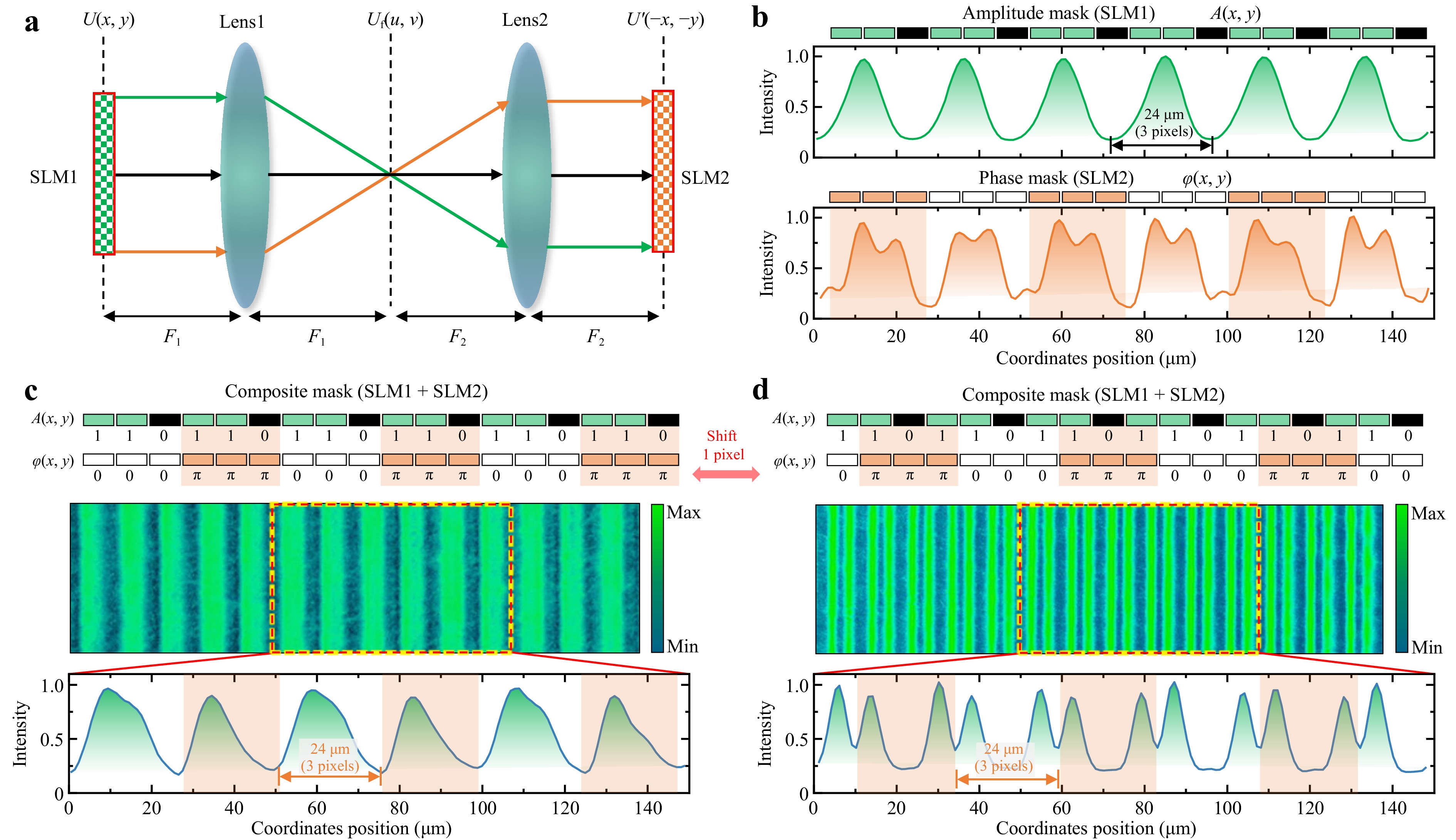
Fig. 2 Light-field amplitude, phase pixelation modulation of digital mask, and pixel-size matching, alignment, and detection. a Optical system of pixel-size matching and alignment. (focal lengths: f1 = 100 mm, f2 = 100 mm). b Measured light-field intensity of digital mask produced via single amplitude-type SLM1 and phase-type SLM2. Amplitude mask (SLM1) is arranged as -1-1-0-(2 pixels (1):1 pixel (0)). Phase mask (SLM2) is arranged as a group of 3 pixels, with alternating 0 and π. c Measured two-dimensional (2D) light-field intensity distribution of composite mask (SLM1+SLM2). Spatial arrangements of amplitude A(x,y) and phase ϕ(x,y) are -1-1-0-1-1-0- and -0-0-0-π-π-π-, respectively. d Measured 2D light-field intensity distribution of composite mask (SLM1+SLM2). Spatial arrangements of amplitude A(x,y) and phase ϕ(x,y) are -1-1-0-1-1-0- and -0-π-π-π-0-0-, respectively. Pixels in phase are shifted by one unit, as compared with Fig. c.
The pixels of the two SLMs were aligned using a six-axis optical adjustment mount, as shown in Fig. S2. By loading the corresponding patterns onto the amplitude- and phase-type LCOS-SLMs, the position of the phase-modulation optical-intensity trough aligned with the position of the pure amplitude optical-intensity trough, thus achieving a programmable ‘digital phase shift mask’. At this point, the phase-shift pattern loaded onto the phase-type LCOS-SLM—featuring 0 and π phase transitions—aligns precisely between the two bright patterns of the amplitude-type LCOS-SLM. The captured optical field exhibits a periodic characteristic with a 24 μm (3-pixel) interval, similar to the single amplitude modulation optical field (Fig. 2b top), as shown in Fig. 2c. Simultaneously, using the six-axis optical adjustment mount (AMM6-1A, LBTEK) for the precise translation of one pixel (8 μm), the 0 and π phase transitions of the phase-type LCOS-SLM are shifted to the exact centre of the bright pixel (1 pixel) in the amplitude pattern. This splits the original two-pixel peak into two single peaks. Compared with the alignment presented in Fig. 2c, the number of peaks in the optical field doubled, as shown in Fig. 2d. At this point, one may conclude that a one-pixel alignment deviation exists between the two LCOS-SLM pixels relative to the target PSM configuration (see Fig. S7).
-
To demonstrate the advantages of phase-shift masks over conventional amplitude masks in projection lithography, we first investigated the lithographic limits of periodic line patterns with either pure amplitude or phase modulation. When using the amplitude-type LCOS-SLM to load different patterns, the phase-type LCOS-SLM loaded patterns with a greyscale value of 0. In this default configuration, the system does not apply phase modulation to the optical field; this is referred to as pure amplitude modulation. Conversely, when using the phase-type LCOS-SLM to load different patterns, the amplitude-type LCOS-SLM loaded patterns with a greyscale value of 255. In this case, the system does not apply amplitude modulation to the optical field and uniformly outputs the maximum amplitude; this is referred to as pure phase modulation. Fig. 3a shows the exposure results for pure amplitude modulation when the amplitude-type LCOS-SLM loaded 2-pixel-wide lines with line spacings ranging from 1 to 8 pixels, which corresponds to periods from 3 to 10 pixels. Under experimental conditions with an incident laser power of 2.84 mW and an exposure time of 40 s, for 2-pixel-wide digital mask line patterns, the photoresist line widths ranged from 144 to 159 nm, while the experimental period widths varied from 391 to 768 nm. When the line period reduced to less than 4 pixels, the line arrays merged and became indistinguishable.
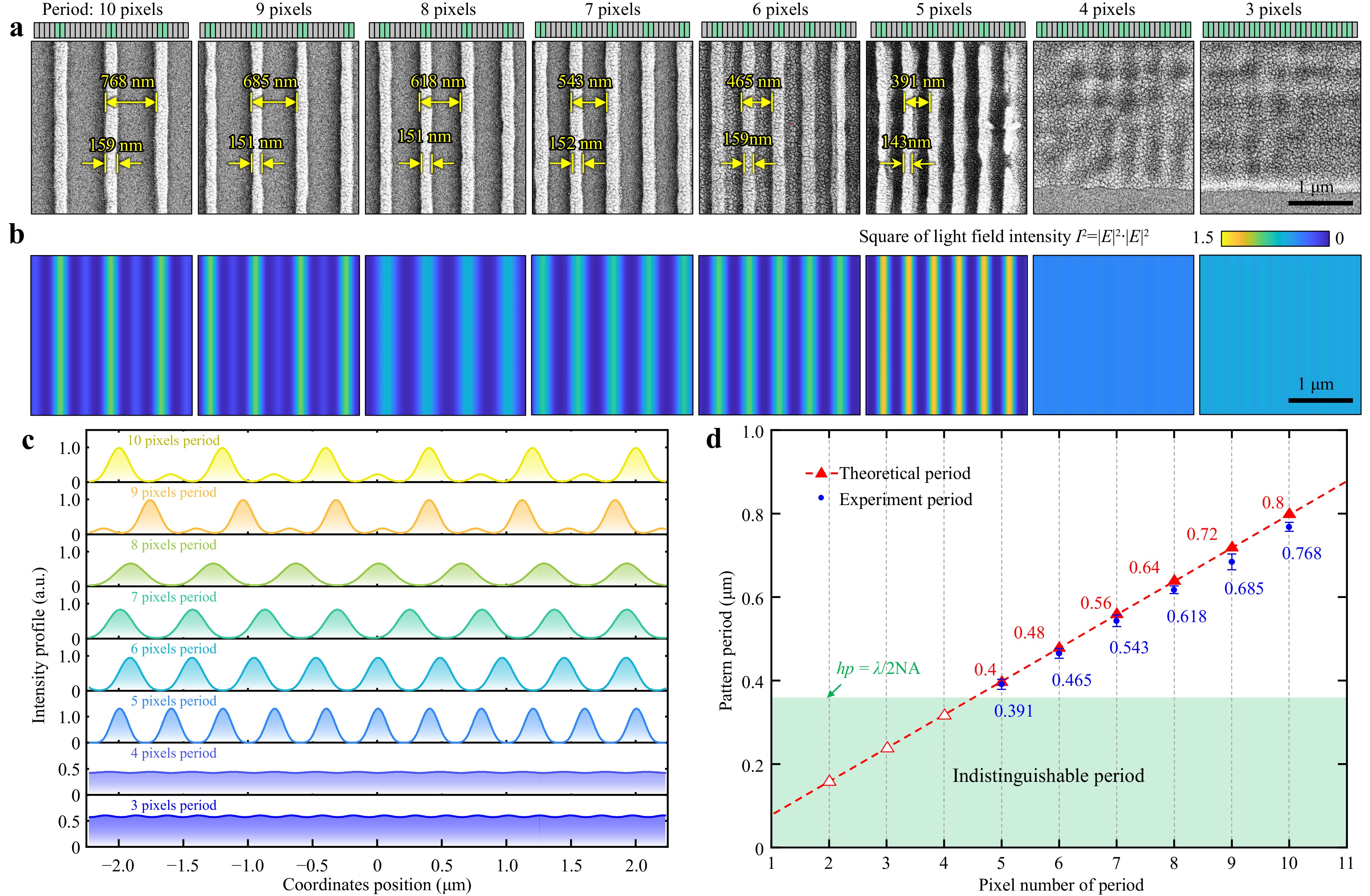
Fig. 3 Exposure results of different periodic line patterns under pure amplitude modulation. a Scanning electron microscopy images of photoresist patterns exposed by pure amplitude digital masks with different periodic line patterns ranging from 10 to 3 pixels. b Theoretically calculated 2D optical-field distribution for different periodic line patterns. c Theoretically calculated intensity profiles for different periodic line patterns. d Comparison of theoretical and experimental periodic widths for 2-pixel wide lines with pure amplitude modulation at different pixel periods. Periods smaller than 5 pixels are defined as forbidden periods.
We computed the focal-plane optical-field distributions for lines with different periods while considering the two-photon nonlinear absorption effect11,12. We plotted the square of the optical intensity distribution (see Supplementary Note 5 for the detailed calculation method), as shown in Fig. 3b. Theoretical calculations indicate that, in the absence of a phase-shift mask, the minimum pattern period that can be exposed was 400 nm (~1.1λ/NA), corresponding to a 5-pixel period line pattern mask. This conclusion represents ‘the general sparrow criterion’ for parallel projection lithography (see Supplementary Note 6 and Fig. S8)12,32,33. As the line period continued to decrease, the optical fields overlapped and became indistinguishable (see Fig. 3c). The theoretically and experimentally obtained line periods increased linearly with the number of pixels, which were slightly smaller than the theoretical period (Fig. 3d). This discrepancy arises from the scaling-factor correction of the projection imaging system, i.e. 1/102× (Fig. S9), which is consistent with theoretical predictions. When the line period decreased to 4 pixels and below, the half-pitch of the lines (hp) became smaller than 0.5 λ/NA, thus appearing in the forbidden period33–36. Consequently, the digital mask cannot be sharply imaged in the photoresist through the projection lens, which implies that the lines cannot be exposed effectively.
In this projection optical system, the resolution limit of the line pitch for pure amplitude modulation is 400 nm (~1.1 λ/NA)12,36. Amplitude-only modulation can yield complex topological patterns within the ultimate resolution. By contrast, the resolution limit of the line pitch for phase-only modulation is 240 nm (~0.67 λ/NA), as shown in Figs. S10 and S11, which corresponds to the phase LCOS-SLM loaded with a half-pitch 3-pixel pattern. However, phase-only modulation cannot generate complex topological patterns independently, and the achieved structural width is larger. The PSM modulation technique complements the advantages of both techniques by achieving a smaller resolution while maintaining the independence and integrity of the patterns. Considering the example of loading a 2-pixel wide line with a 3-pixel pitch using amplitude modulation, the phase-type SLM must load a 3-pixel pitch line pattern with phases 0 and π arranged alternately to achieve a phase difference Δϕ of π between adjacent lines, as shown in the top inset of Fig. 4a-c. The loaded patterns of the phase-type SLM are half the period of the loaded pattern of the amplitude-type SLM. This arrangement ensures that adjacent periods of the amplitude pattern have a phase difference of π.
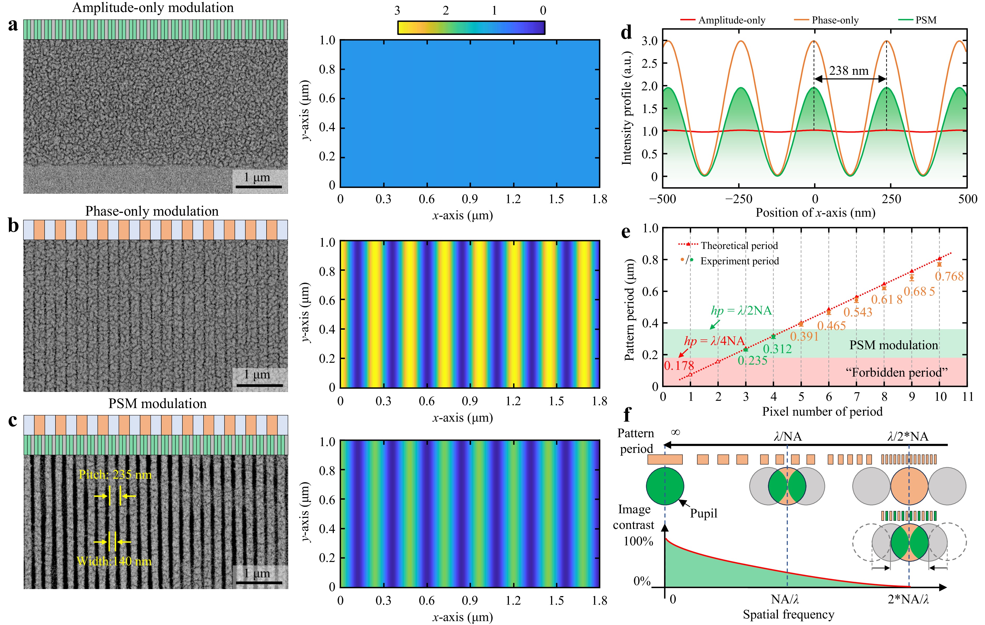
Fig. 4 Comparative analysis of exposure results for periodic line-space patterns generated using digital mask strategies. a SEM images and simulated optical-field distribution of periodic lines (2 pixels (255):1 pixel (0)) under amplitude-only modulation. b SEM images and simulated optical-field distribution of periodic lines (3 pixels (0):3 pixels (π)) under phase-only modulation. c SEM images, and simulated optical-field distribution of periodic lines under PSM modulation. d Comparison of light-intensity profiles for periodic line-space patterns generated using different digital mask strategies. e Relationship between pattern period and pixel count for three types of digital masks. f Modulation transfer function (MTF): contrast loss is proportional to the zero-order light passing through the lens aperture without an interference partner, which only contributes to a constant offset.
-
For the digital mask with a 2-pixel width and 3-pixel pitch, the exposed resist patterns by amplitude-only modulation are indistinguishable, as shown in Fig. 4a, whereas both phase-only and PSM modulations can generate clear and dense line pattern structures, with simulated periods of 238 nm, as shown in Fig. 4d. Based on the experimental results, both methods exhibited a period width of 235 nm, which closely matched the simulation results. However, the linewidths were 214 and 146 nm, respectively, with the alternating PSM technique achieving a narrower linewidth. By adjusting the exposure dose, the CD:gap of the line array pattern was controlled to 1:1 or smaller (Figs. S12 and S13). By combining the simulated and experimental results, we obtained the widths of structures with a 2-pixel width and different pixel periods (see Fig. 4e). For periods greater than 5 pixels (including 5 pixels), amplitude-only modulation can expose dense line patterns. For periods of 3 and 4 pixels, the PSM modulation must achieve clear exposure. For structures with periods smaller than 3 pixels (excluding 3 pixels), because the diffraction limit of this system is 217.5 nm (0.5 λ/NA), none of the methods—pure amplitude modulation, pure phase modulation, or alternating PSM—can produce structures beyond this resolution.
According to the principles of information optics, when light passes through an object and undergoes diffraction, the high-frequency components in the diffraction spectrum contain more detailed information about the object36,37. For digital masks in the form of periodic gratings, the distribution of their diffraction spectrum is centered around the zeroth-order diffraction spectrum and is symmetrical38–40. In a projection lithography system, owing to the low-pass filtering effect in the objective system, only a portion of the diffraction spectrum of the digital mask can be received by the objective and interfere to form an image on the image plane.
In the case of on-axis point-source illumination40–42, when the period of the grating-type mask pattern is such that its first-order diffraction light coincides with the aperture edge of the projection objective, the half pitch of this striped pattern is the maximum resolution that the lithographic system can resolve41, as shown in Fig. 4f and S14. When the half pitch of the striped pattern is smaller than this value, the first-order diffraction light appears outside the aperture of the projection objective, and only the zeroth-order light passes through the projection objective, thus rendering interference imaging on the image plane impossible. Under on-axis point source illumination, the cutoff frequency of the projection system is NA/λ32,33,40-42. This implies that the theoretical resolution limit of a conventional projection lithography imaging system is R = hp (pitch/2) = λ/(2NA), which corresponds to a theoretical period of pitch = λ/NA = 356 nm. For digital phase-shift mask projection lithography, the theoretical resolution limit is R = hp (pitch/2) = λ/4NA, which corresponds to a theoretical period of pitch = λ/(2NA) = 178 nm, as shown in Fig. 4c and S15. The alternating phase-shift mask technique creates phase conflicts between adjacent structures and utilises the dark regions of optical intensity generated by interference cancellation to render the originally indistinguishable structures clear and resolvable.
-
To investigate the relationship between phase shift Δϕ and optical-field distribution in alternating PSM technology, we selected grey levels of 64, 128, 192, and 255, which correspond to phase delays Δϕ of 0.17π, 0.40π, 0.75π, and 1.05π, respectively. A 2-pixel-wide, 4-pixel-pitch array structure was used, with the minimum grey level in the graphics loaded onto the phase-type LCOS-SLM set to 0. The effects of alternating PSM modulation at different maximum phase delays Δϕ were compared, as shown in Fig. 5a, b. As Δϕ approached π, the peak intensity, contrast, and slope between light and dark regions increased continuously and reached maximum values when Δϕ ≈ π. By contrast, pure amplitude modulation and low phase delays (e.g. 0.17π) only marginally resolved the photoresist structures due to low local contrast in the optical field (Fig. 5c). Furthermore, as Δϕ approached π, the number of peaks in the intensity distribution doubled, thus indicating that the highest spatial contrast can be achieved using this configuration.
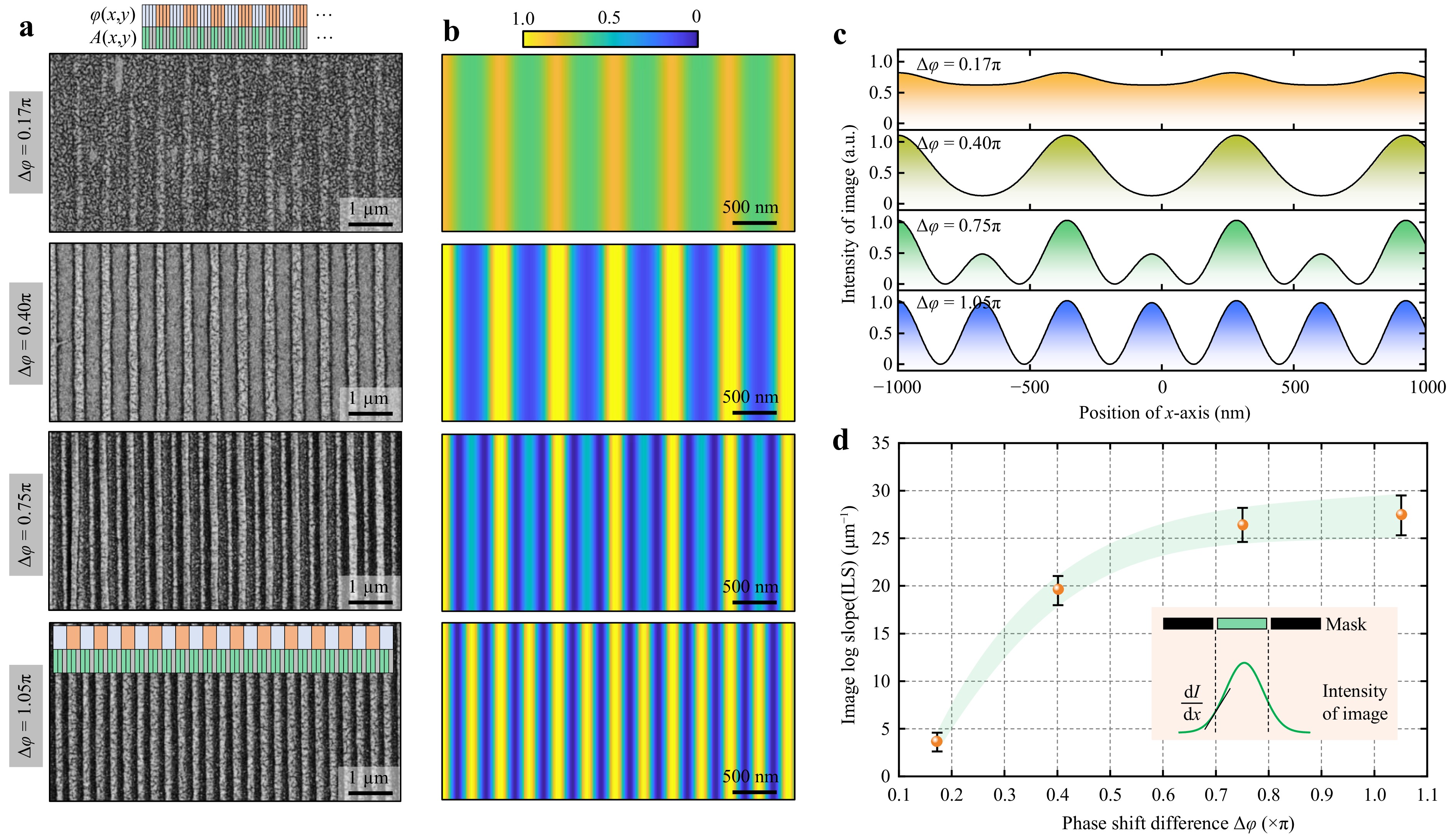
Fig. 5 Comparative analysis of exposure results for extreme periodic lines under phase-shift mask modulation with different phase shifts Δϕ. a SEM images and simulated optical-field distribution of periodic lines under PSM modulation with different phase shift Δϕ ranges from 0.17π to 1.05π. b Simulated optical-field distribution of periodic lines under PSM modulation with different phase shift Δϕ ranges from 0.17π to 1.05π. c Light-intensity profile for periodic line-space patterns with different phase shifts. d Relationship between ILS and phase-shift difference Δϕ. Inset illustrates slope of optical-field intensity.
In photolithography, when controlling the line width of the photoresist pattern exerts a greater effect on lithographic performance, the key metric that affects the lithographic results is the image log slope (ILS) at the ideal linewidth edge43–45. The ILS quantifies the steepness of the intensity transition at feature boundaries and is expressed as
$$ ILS=\frac{1}{I}\cdot \frac{{\rm d}I}{{\rm d}x}=\frac{{\rm d} \text{In}\left(I\right) }{{\rm d}x}$$ (6) Typically, the ILS is evaluated at the mask-pattern boundary (see inset of Fig. 5c). For structures with pitches of 3–4 pixels, pure amplitude modulation alone caused a rapid decrease in the optical-field contrast after passing through a 1/100× objective, thus rendering it difficult to clearly resolve bright and dark stripes.
In this study, the ILS is used as a quantitative metric to guide the optimisation of Δϕ in phase-modulated exposures. A higher ILS corresponds to a steeper intensity gradient, which enhances the pattern contrast and reduces the linewidth. As Δϕ approaches π, destructive interference between adjacent pixels suppresses sidelobes and creates more pronounced intensity minima, thus resulting in sharper feature edges and higher ILS values. Therefore, the optimal Δϕ is determined by maximising the ILS, thereby effectively improving both imaging contrast and resolution.
-
This study demonstrates a digital projection lithography approach based on PSM modulation, which achieved a pitch resolution of 235 nm with a single exposure, i.e. a value close to the physical resolution limit of digital lithography4,12,36. We validated the feasibility of using PSM digital lithography for integrated circuit patterning by fabricating two representative metal-layer layouts (Fig. 6a, b) and a grating map (Fig. S16). For the dense regions of the ordered layout shown in Fig. 6a, S17a, and S18, PSM lithography enabled the effective exposure of features that were otherwise unresolvable. Even in the unordered layout presented in Fig. 6b and S17b, the method successfully generated numerous dense lines with an interline pitch of 276 nm, which is below the diffraction limit of λ/NA.
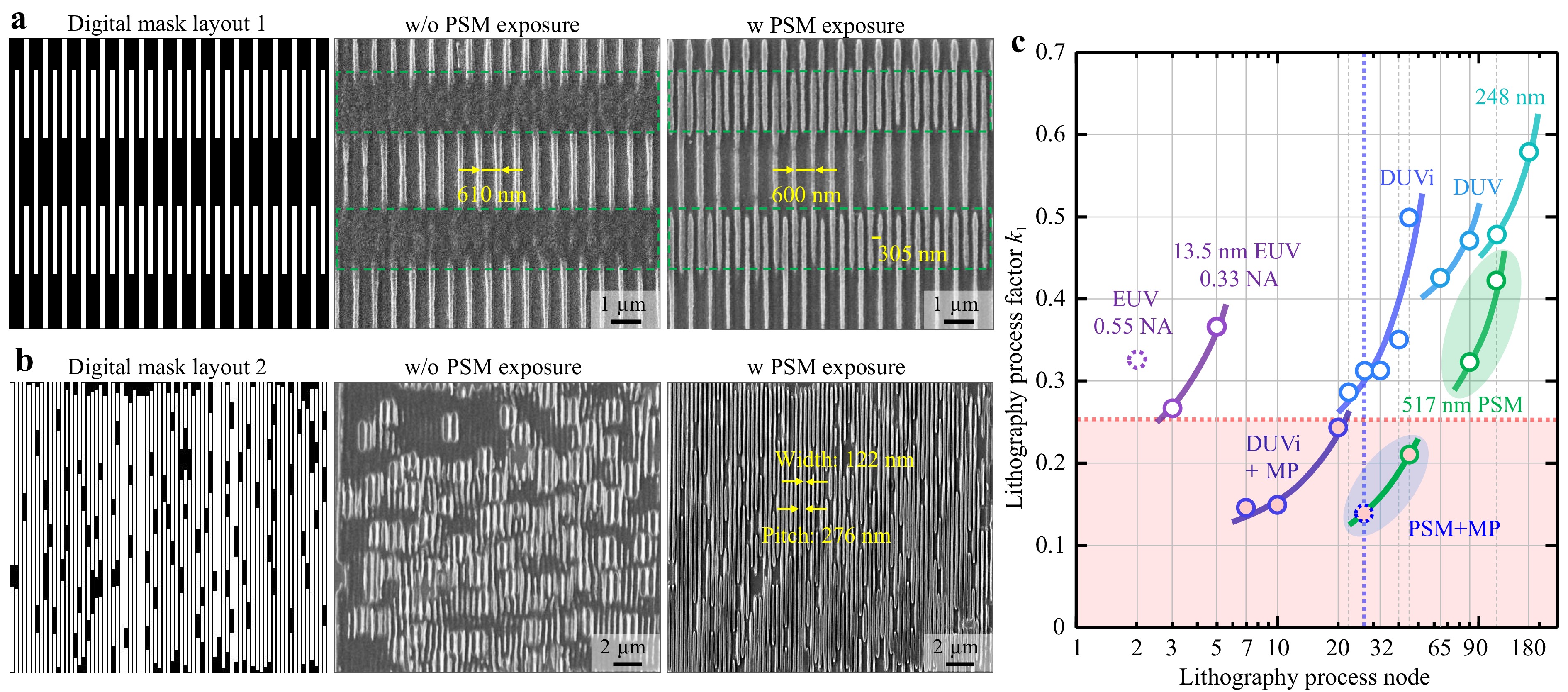
Fig. 6 Performance (pitch resolution) comparison for chip metal-layer layout. a Digital mask and SEM images of ordered layout. b Digital mask and SEM images of unordered layout. c Statistical results of pitch-resolution and process factor of DMPL compared with 248 and 193 nm deep-ultraviolet (DUV) and extreme ultraviolet (EUV) lithography.
Compared with the case of conventional photolithography, as shown in Fig. 6c, the achieved resolutions correspond to the 130 and 90 nm technology nodes (green area), thus highlighting the potential of this method as a viable alternative for chip patterning at the 90 nm node46–50. Combining the method with the multiple exposure process12,36, the pitch can reach 158 nm with double exposure (Fig. S19). If the method is further replaced with 400 nm laser exposure, then a 28 nm lithography process node (blue area) can be expected.
Unlike conventional lithography, the proposed digital PSM lithography technique is maskless, inexpensive, highly flexible, and customisable. These features significantly simplify the fabrication process, reduce the time from chip design to prototyping, and reduce research and development costs15,26. This technology provides a novel solution for multi-variety, small-batch, and customised chip fabrication, and establishes a promising foundation for future high-precision manufacturing at sub-100 nm scales.
Additionally, the arbitrary and independent control of both amplitude and phase provided by the dual-SLM platform renders this DMPL approach particularly suitable for fabricating complex, nonperiodic micro-nano optical components, such as metasurfaces and diffractive optical elements. Future studies will focus on system optimisation and process refinement to further improve pattern fidelity and fabrication stability. Additionally, integration with other advanced manufacturing techniques, such as multiphoton polymerisation and deep ultraviolet lithography, will also be explored to broaden the applicability of this approach to broader nanofabrication scenarios.
-
In this study, we developed PSM-DPL technology by combining the flexibility of SLMs with the resolution-enhancing advantages of conventional PSM techniques, thereby enabling the efficient fabrication of subwavelength-scale dense line patterns. Experimental results demonstrate that this technology can achieve line patterns with a feature width of ~60 nm (CD ~0.16 λ/NA) and a pitch resolution of ~235 nm (hp ~0.32 λ/NA) in a single exposure, thus approaching the physical resolution limit of digital lithography. Through double exposure, the achievable pitch resolution was further improved from 235 to 158 nm, thereby validating the feasibility of this method for patterning metal layers of integrated circuits. By precisely controlling the phase difference (Δφ = π) between adjacent patterns and leveraging destructive interference effects, imaging contrast and resolution are enhanced. Both experimental and simulation results confirm that when the phase difference approaches π, the contrast of the optical-field distribution and the ILS reach their optimal values, thus achieving resolution near the diffraction limit.
Compared with conventional lithography techniques, digital PSM lithography offers several distinct advantages. First, its maskless nature eliminates the necessity for expensive physical mask fabrication, thereby substantially reducing both development time and expenses. Second, the use of a programmable SLM enables high patterning flexibility, thus allowing the rapid generation of arbitrarily complex designs and rendering the approach particularly suitable for multi-variety, small-batch, and customised chip fabrication. Third, the technique is compatible with a wide range of illumination sources spanning from visible to ultraviolet wavelengths, thereby facilitating seamless integration with other advanced manufacturing platforms, including multiphoton polymerisation and deep ultraviolet lithography. Collectively, these advantages highlight the strong potential of digital PSM lithography as a versatile and cost-effective strategy for fabricating subwavelength-scale line patterns. Beyond providing a promising alternative to conventional lithographic methods, this approach can facilitate high-density integrated circuit manufacturing and the development of broader micro- and nanofabrication applications.
-
We used a complex amplitude-modulation digital-mask projection lithography system equipped with an ultrafast fibre femtosecond laser system (Huaray Precision Laser Co., Ltd.), which delivered a repetition rate of f = 10 MHz, a central wavelength of 517 nm, and a pulse duration of 240 fs, as shown in Fig. S1. After the outgoing laser beam was expanded and homogenised, it entered the complex amplitude-modulation system. Some of the energy of the complex amplitude-modulation light field entered the charge-coupled device (CCD) to achieve real-time observation of the light field during lithography. The main light energy entered the oil-immersed objective lens (100×, NA 1.40, Nikon) to transfer the scaled image to the photoresist surface. In this system, tube lens1 and lens2 were exactly the same tube lenses (TTL100-A, Thorlabs). Unlike ordinary lenses, the main imaging system used tube lenses to reduce imaging aberrations. The photoresist substrate was placed on an electrically controlled translation stage. The translation stage can be a three-dimensional translation stage (AG10010H, OptoSigma) with an XY-plane displacement accuracy of 1 µm and a high Z-axis displacement accuracy of 0.1 µm. Combined with real-time CCD observations, the optimal focal position of the lithography process can be guaranteed.
-
AR-N 7520 (Allresist GmbH) was used as the photoresist in the experiment. The photoresist film was prepared via spin coating at 5,000 rpm for 1 min using a spin coater (MIDAS SYSTEM SPIN-1200T) on a glass substrate, thus resulting in a photoresist thickness of 260 nm. Subsequently, the coated substrate was prebaked on a hot plate at 85°C for 1 min. After photoresist exposure, post-bake was not required. Instead, the substrate was directly immersed in an AR300-47 developer solution (Allresist GmbH) for 90 s. Subsequently, the residual developer solution on the glass substrate was rinsed with deionised water, and the surface was dried by blowing nitrogen gas. This process resulted in the formation of a photoresist pattern on the substrate.
-
Surface and feature-scale analyses of line-array patterns were performed using a field-emission scanning electron microscope (Thermo Scientific FEI, Apreo 2 SEM). The thickness of the photoresist film was measured using a probe surface profilometer (KLA-Tencor Corp., AlphaStep P-7).
-
This study was supported by the National Key Research and Development Program of China (2016YFA0200500), the National Natural Science Foundation of China (62575128), the Major Talent Program of Guangdong Province (2019CX01Z389), the Science and Technology Planning Project of Guangzhou (202007010002), and the Guangdong Basic and Applied Basic Research Foundation (2023A1515011404).
Digital phase-shift mask projection lithography enabling sub-diffraction-limit resolution for dense nanoscale patterning
- Light: Advanced Manufacturing , Article number: 80 (2026)
- Received: 07 February 2026
- Revised: 30 April 2026
- Accepted: 07 May 2026 Published online: 18 June 2026
doi: https://doi.org/10.37188/lam.2026.080
Abstract: The diffraction limit poses a fundamental challenge to digital mask projection lithography (DMPL) in fabricating subwavelength-scale dense periodic patterns, limiting its application in advanced chip manufacturing. To address this, we present a DMPL platform with a resolution-enhancement strategy combining a digital phase-shifting mask with two-photon polymerisation. The method enables precise control of subwavelength structure distribution while preserving DMPL flexibility. Using alternating phase-shifting modulation through cascaded spatial light modulators under 517 nm femtosecond laser illumination, we achieve near-physical-limit resolution in a single exposure, producing line patterns with a critical linewidth of ~60 nm (0.16 λ/NA) and a single-exposure pitch resolution of ~235 nm (half pitch ~0.32 λ/NA). With a double-exposure strategy, the pitch is further reduced to ~158 nm (half pitch ~0.21 λ/NA), enabling robust sub-diffraction-limit patterning. This approach advances diffraction-limited patterning and offers new possibilities for manufacturing nanophotonic devices and next-generation microelectronic components.
Research Summary
Digital phase-shift masks push maskless lithography beyond conventional diffraction limits
A programmable lithography platform that combines digital phase-shift masks with two-photon polymerization achieves dense nanoscale patterning at resolutions previously inaccessible to maskless projection systems. Yuan-Yuan Zhao from Jinan University used two cascaded spatial light modulators to independently control amplitude and phase, introducing alternating π phase shifts between adjacent features to enhance destructive interference and sharpen image contrast. The system produced line widths of ~60 nm and single-exposure pitch resolution of ~235 nm under 517 nm femtosecond illumination, with double exposure further reducing pitch to ~158 nm. The team also demonstrated fabrication of representative chip metal-layer layouts, highlighting potential for rapid prototyping of integrated circuits, metasurfaces, and other high-density nanophotonic devices.
Rights and permissions
Open Access This article is licensed under a Creative Commons Attribution 4.0 International License, which permits use, sharing, adaptation, distribution and reproduction in any medium or format, as long as you give appropriate credit to the original author(s) and the source, provide a link to the Creative Commons license, and indicate if changes were made. The images or other third party material in this article are included in the article′s Creative Commons license, unless indicated otherwise in a credit line to the material. If material is not included in the article′s Creative Commons license and your intended use is not permitted by statutory regulation or exceeds the permitted use, you will need to obtain permission directly from the copyright holder. To view a copy of this license, visit http://creativecommons.org/licenses/by/4.0/.

 DownLoad: