






-
Metalenses consist of arrays of subwavelength nanostructures, termed meta-atoms1–5. Compared with traditional optical lenses, they are incredibly thin and have high design flexibility, rendering them highly promising for the miniaturisation of optical systems6–14. However, chromatic aberration in metalenses significantly degrades their imaging quality15–20. Various design strategies have been proposed to address this problem21–24. Chen et al. combined geometric and propagation phases to achieve excellent achromatic performance23. Nevertheless, this scheme imposes extremely stringent requirements on both the angular and dimensional precision of the meta-atoms. This poses considerable challenges for the fabrication of metalenses, particularly for large-scale production. Electron beam lithography (EBL) defines patterns using accelerated electrons with an extremely short de Broglie wavelength, thereby enabling an ultrahigh nanoscale resolution and high fidelity. Consequently, it enables the fabrication of metalenses whose performance closely matches that of theoretical simulations24. However, its point-by-point scanning mechanism results in low throughput and high costs, limiting its large-scale application25. In contrast, deep ultraviolet (DUV) lithography is based on mature semiconductor technology and achieves large-area pattern transfers through step-and-repeat mask exposure, thereby enabling the large-scale manufacturing of metalenses26,27. However, the high equipment cost and complex process flow (including the deposition of dielectric materials, DUV, etching, and photoresist stripping) restrict its widespread adoption, particularly in applications requiring low-cost metalenses. Therefore, the development of strategies for both large-area and cost-effective fabrication is crucial as it can aid in overcoming the industrialization bottleneck of metalenses.
Nanoimprint lithography (NIL), a one-step micro/nanofabrication technology, is an ideal method for the low-cost production of metalenses28–30. In this process, meta-atom structures are first fabricated on a master and repeatedly replicated on working stamps. The working stamps can then be employed to imprint multiple metalens wafers in which a high-refractive-index nanoimprint photoresist serves as the meta-atom material31,32. This NIL-based fabrication method can reduce production costs and significantly improve manufacturing efficiency. In recent years, researchers have utilised NIL to fabricate metasurfaces based on nanoimprint photoresists with a refractive index of ~1.9, achieving functionalities including single-wavelength focusing33,34, holographic display35–39, full-space diffractive40, and light-emitting41. However, nanoimprint photoresists commonly suffer from excessive structural shrinkage after curing, with reported shrinkage values as high as ~20% in some studies (see Table S1)33,34. Excessive structural shrinkage compromises fabrication precision and restricts the design range of meta-atom dimensions. This effect is particularly pronounced for metalenses designed based on the propagation phase. Therefore, the development of nanoimprint photoresists with high refractive index, high transmittance, and low shrinkage, as well as their associated working stamps and NIL processes, holds significant research and application value in metalens fabrication.
In this study, an achromatic metalens was achieved through scalable nanoimprint manufacturing based on a high-refractive-index and low-shrinkage photoresist, as shown in Fig. 1a. A nanoimprint photoresist based on a mixture of acrylate polymers, TiO2 nanoparticles, silane, and methacryl-functionalized silane was used as the meta-atom material. The silane and methacryl-functionalized silane were incorporated into the photoresist to limit its shrinkage rate to no more than 5.19% in both the lateral and longitudinal directions. With the incorporation of TiO2 nanoparticles, the photoresist exhibited a high refractive index (>1.9) and high light transmittance (>99%) in the 480–640 nm wavelength range. Based on this nanoimprint photoresist and by combining the principles of the propagation and geometric phases, we designed an achromatic metalens with a minimum structural width of 166 nm, minimum spacing of 120 nm, and maximum aspect ratio of 8:1. A schematic of the fabrication process is shown in Fig. 1b. Using a highly precise and fast-curing ultraviolet (UV) material, we completed the fabrication of the working stamps within 10 min. Compared with the traditional polydimethylsiloxane (PDMS)-based33,34 process, which requires several hours, this method significantly improves fabrication efficiency. The fabricated metalens demonstrates excellent focusing performance and an achromatic effect, with a maximum focal length deviation of less than 2% for different wavelengths in the 480–640 nm range. The results of this study provide a feasible solution for the high-precision, high-efficiency, and large-scale fabrication of achromatic metalenses and has important applications in fields such as imaging, displays, and optical communication.
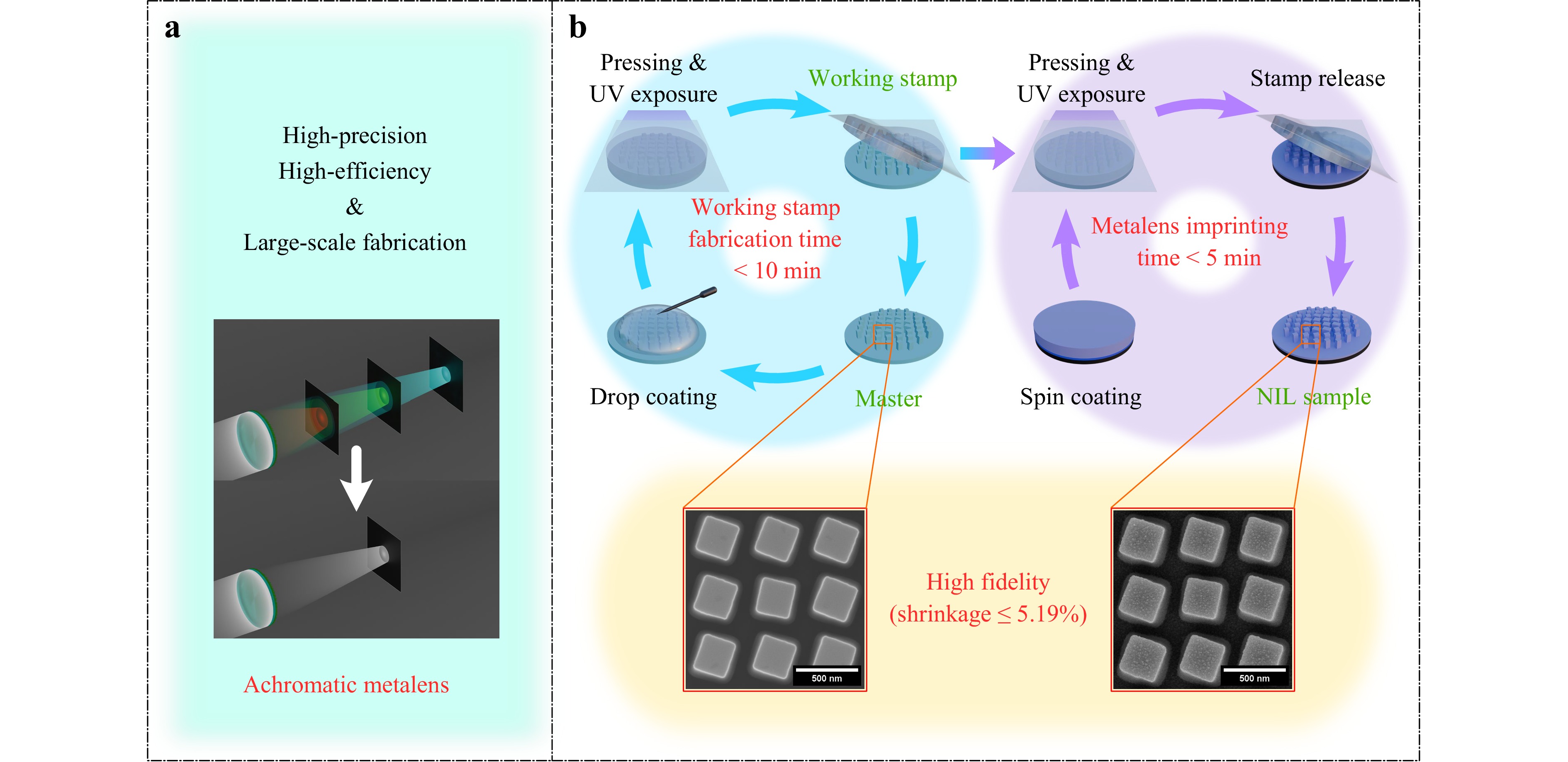
Fig. 1 Schematic of the fabrication process for achromatic metalenses based on a high-refractive-index and low-shrinkage nanoimprint photoresist. a Schematic of the achromatic metalens. b Schematic of the high-precision, high-efficiency, and large-scale fabrication process of achromatic metalenses.
-
In this study, a nanoimprint photoresist (O2190, OuGuangXin Technology) containing an acrylate polymer, TiO2 nanoparticles, silane, and methacryl-functionalized silane was employed and characterised for subsequent experiments, as shown in Fig. 2. The detailed preparation procedures are provided in the Materials and Methods section.
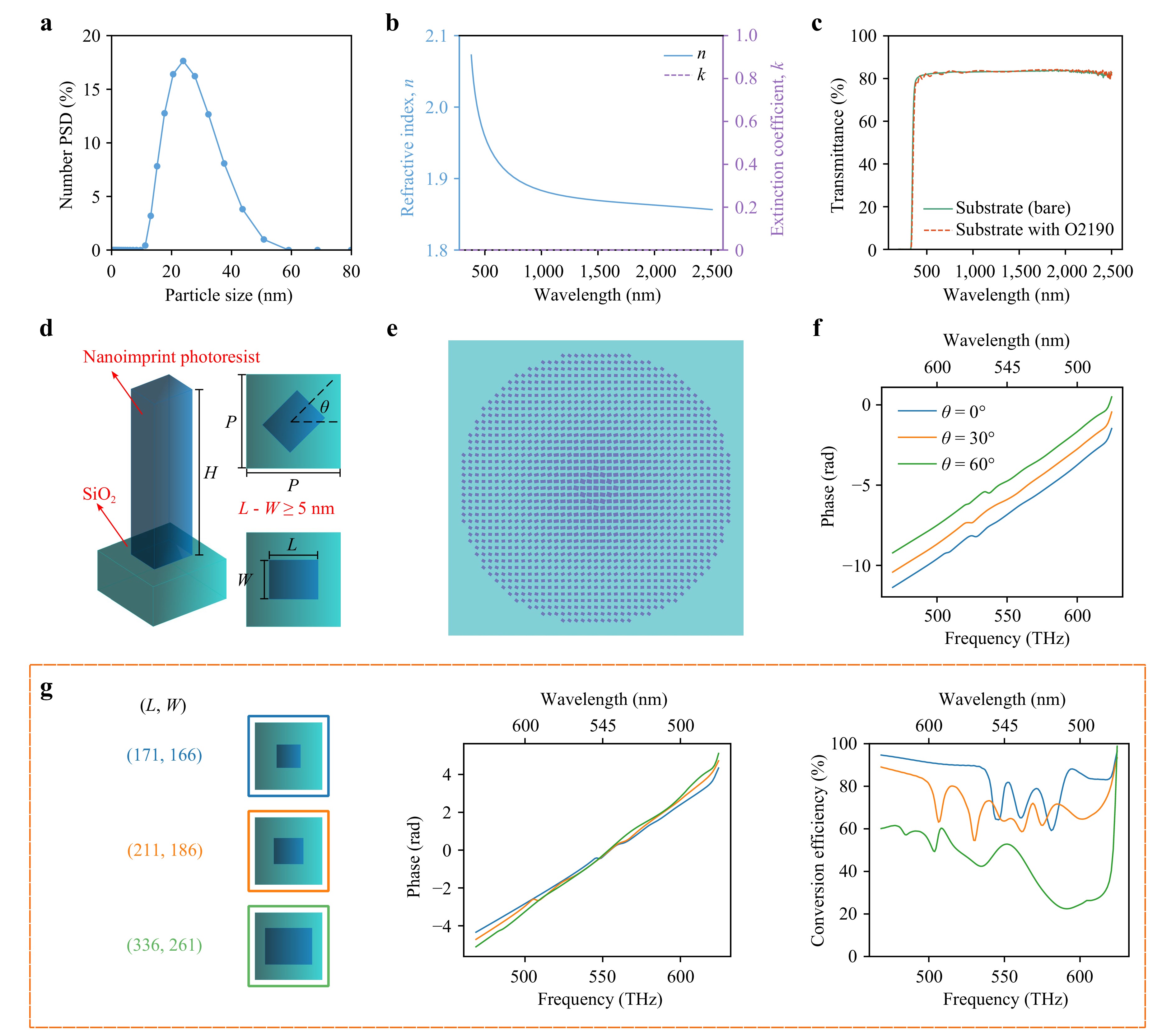
Fig. 2 Characterization of the high-refractive-index nanoimprint photoresist (O2190) and design schematics of the achromatic metalens. a DLS particle size distribution curve of TiO2 nanoparticles in the nanoimprint photoresist. The Z-average particle size is 26.24 nm, and the PDI is 0.2334. b Refractive index and extinction coefficient at wavelengths of 380–2,500 nm. c Optical transmittance at wavelengths of 200–2,500 nm. d Schematic of the meta-unit design: the substrate material is SiO2, with a period of P = 480 nm; the meta-atom material is the nanoimprint photoresist, with a height of H = 1,000 nm, rotation angle of θ, length of L, and width of W. e Top view of the designed achromatic metalens structure. f Phase curves of the meta-atom versus frequency at different rotation angles, with the dimension parameters of L = 336 nm and W = 166 nm. g Comparison of phase spectra and polarization conversion efficiencies for three typical meta-atoms based on the structure in (d) with a fixed rotation angle θ = 0°. Each coloured curve corresponds to the meta-atom structure in the left schematic. The (L, W) parameters of the three meta-atoms are (171, 166), (211, 186), and (336, 261) in nanometres. The three structures exhibit distinct group delays and polarization conversion efficiencies.
In the nanoimprint photoresist, silane and methacryl-functionalized silane enhance the strength of the photoresist, reduce shrinkage, and improve substrate adhesion. Silane coupling agents act as molecular bridges; their hydrolysable alkoxy groups form robust Si-O-Si bonds with the inorganic phases, whereas their polymerisable termini copolymerise into the acrylate network. This dual-bonding effect anchors the rigid inorganic phase to the polymer matrix, restricts the polymer chain mobility, and thereby reduces shrinkage42. Moreover, the relatively long and flexible structure of the methacrylic acid-functionalized silanes modulates the crosslinked network, promoting a more relaxed pre-gel state that facilitates internal rearrangement during curing to relieve stress and further suppress polymerization-induced shrinkage43. To evaluate these effects, we prepared two samples using the same grating master, with and without additives, and characterised them using scanning electron microscopy (SEM). As shown in Fig. S1, the structures fabricated with additives were noticeably larger than those without additives, confirming the effective suppression of shrinkage. Furthermore, the TiO2 nanoparticles increase the refractive index of the nanoimprint photoresist. A higher mixing ratio of these nanoparticles results in a higher refractive index of the photoresist, whereas an excessively high mixing ratio can impair its fluidity. An optimal component mixing ratio is required to balance these two properties. Additionally, for effective filling of nanostructures (meta-atoms) during the nanoimprint process, the nanoparticles must be of an appropriate size. As shown in Fig. 2a, the dynamic light scattering (DLS, Malvern Zetasizer Pro) results revealed that the size of the TiO2 nanoparticles was primarily distributed in the range of 10–60 nm, with a Z-average particle size of 26.24 nm and polydispersity index (PDI) of only 0.2334. This indicates that the TiO2 particles in the nanoimprint photoresist are smaller than the minimum meta-atom size and are uniformly dispersed without apparent agglomeration. Such a particle distribution not only provides extremely low optical scattering loss but also ensures complete filling of the meta-atom structures during the nanoimprinting process.
The refractive index and extinction coefficient of the nanoimprint photoresist were measured using an ellipsometer (RC2-XI, J.A. Woollam), and the results are shown in Fig. 2b. Fig. S2 shows the original ellipsometry test spectra and fitting procedure. Within the 480–640 nm wavelength range, the photoresist exhibits a high refractive index (1.92–1.97); moreover, an extinction coefficient of nearly 0 indicates no significant light absorption.
To evaluate the optical transmittance of the nanoimprint photoresist, we prepared two samples for comparison. The first sample was a bare glass substrate (n ≈ 1.9), whose transmission spectrum served as the baseline reference. The second sample was a glass substrate spin-coated with the nanoimprint photoresist. The nanoimprint photoresist was deposited on the same glass substrate and UV-cured under actual fabrication conditions (exposure wavelength: 365 nm, power: 300 W, duration: 30 s) to form a ~1 μm-thick nanoimprint photoresist film. The transmittance and haze were measured using a UV-Vis-NIR spectrophotometer (Lambda1050+, PerkinElmer). As shown in Fig. 2c, their transmission spectra overlapped strongly in the designed operating wavelength range (480–640 nm). The average transmittance of the bare substrate was 82.29%, whereas that of the flat photoresist film was 82.13%. After normalisation to the baseline reference, the relative transmittance of the 1 μm-thick photoresist film exceeded 99%, demonstrating its excellent visible-light transmittance and low absorption characteristics. Fig. S3 shows the haze distribution in the 380–780 nm wavelength range, with an average haze of only 0.38%, indicating that the nanoimprint photoresist exhibited very low optical scattering.
To verify the feasibility of the aforementioned material for high-throughput fabrication of metalenses, we designed a broadband visible-light achromatic metalens and simulated its optical performance. The target phase distribution of an ideal metalens can be expressed as23
$$ \phi \left(\omega ,r\right)=-\frac{\omega }{c}\left(\sqrt{{r}^{2}+{f}^{2}}\right)+C\left(\omega \right)$$ (1) where $ \omega $ is the angular frequency, $ r $ is the distance from the meta-unit on the metalens to its centre, $ c $ is the speed of light, $ f $ is the focal length, and $ C\left(\omega \right) $ provides a new degree of design freedom for phase modulation. The optimal value of $ C\left(\omega \right) $ was solved using an optimisation algorithm44, which enabled us to optimise the performance of the achromatic metalens.
We designed the achromatic metalens by combining the propagation and geometric phases, as described in the Materials and Methods section. A schematic of the material and geometric parameters of the meta-atom is shown in Fig. 2d. The substrate was fused silica (SiO2), and the meta-atom structure was composed of a high-refractive-index nanoimprint photoresist. The period (P) and height (H) were fixed at 480 and 1,000 nm, respectively, whereas the length (L) and width (W) varied within 176–336 nm and 166–326 nm, respectively. The phase and polarisation conversion efficiency distributions for different dimensions are shown in Fig. S4. Meanwhile, geometric phase modulation could be achieved by rotating the meta-atom angle θ. Fig. 2f shows the phase spectra of the meta-atoms at different rotation angles. Within a specific bandwidth, the slopes of these spectra were approximately linear and independent of the meta-atom rotation angles. Fig. 2g compares the phase spectra and polarisation conversion efficiencies of three meta-atoms with different dimensions at θ = 0°. The different-coloured curves correspond to the meta-atom structures shown in the schematic, and the (L, W) parameters of each structure are shown in the figure. The group delay was obtained through the linear fitting of the phase spectra23. Based on the above characteristics, precise control of phase and group delay could be achieved by independently tuning the rotation angle (θ) and geometric dimensions (L and W) of the meta-atoms. Based on these principles, the designed achromatic metalens has a diameter D of 20 μm, and its structural schematic diagram is shown in Fig. 2e.
The design and simulation details of the entire metalens are provided in the Materials and Methods section, Fig. S5, and Table S2. These results demonstrate that the designed metalens achieves high achromatic performance: Within the entire designed wavelength range, the maximum deviation of the focal length is less than 2% of the designed focal length.
The designed metalens was fabricated using NIL technology, with the process flow described in the Materials and Methods section and Fig. S6. First, a Si-based master material was prepared using EBL and inductively coupled plasma (ICP) etching. Subsequently, the working stamp was replicated using a novel UV-curable resin (WSA08), which enabled rapid solidification within 3 min. This is markedly faster than the commonly used heat-cured PDMS, which typically requires several hours, and thus significantly improves fabrication efficiency31. Finally, the metalens, based on the previously described nanoimprint photoresist (O2190), was fabricated via the NIL process using this working stamp. The entire NIL process can be completed in 5 min, and the working stamp can be reused multiple times, providing support for the low-cost large-scale production of metalenses.
To investigate the fabrication accuracy, we characterized the top and cross-sectional views of the meta-atom structures for the master, working stamp, and NIL sample using SEM and focused ion beam scanning electron microscopy (FIB-SEM), as shown in Fig. 3. The top-view SEM images showed that each meta-atom in the NIL sample remained intact with a clear outline and without any defects such as structural loss, collapse, or residual adhesive. The fabrication successfully achieved structural gaps as small as ~120 nm, demonstrating the capability of processing aspect ratios of nearly 8:1. The FIB-SEM cross-sectional images indicated that the meta-atom sidewalls of the master exhibited a slight tilt, forming an angle of 87° with the substrate.
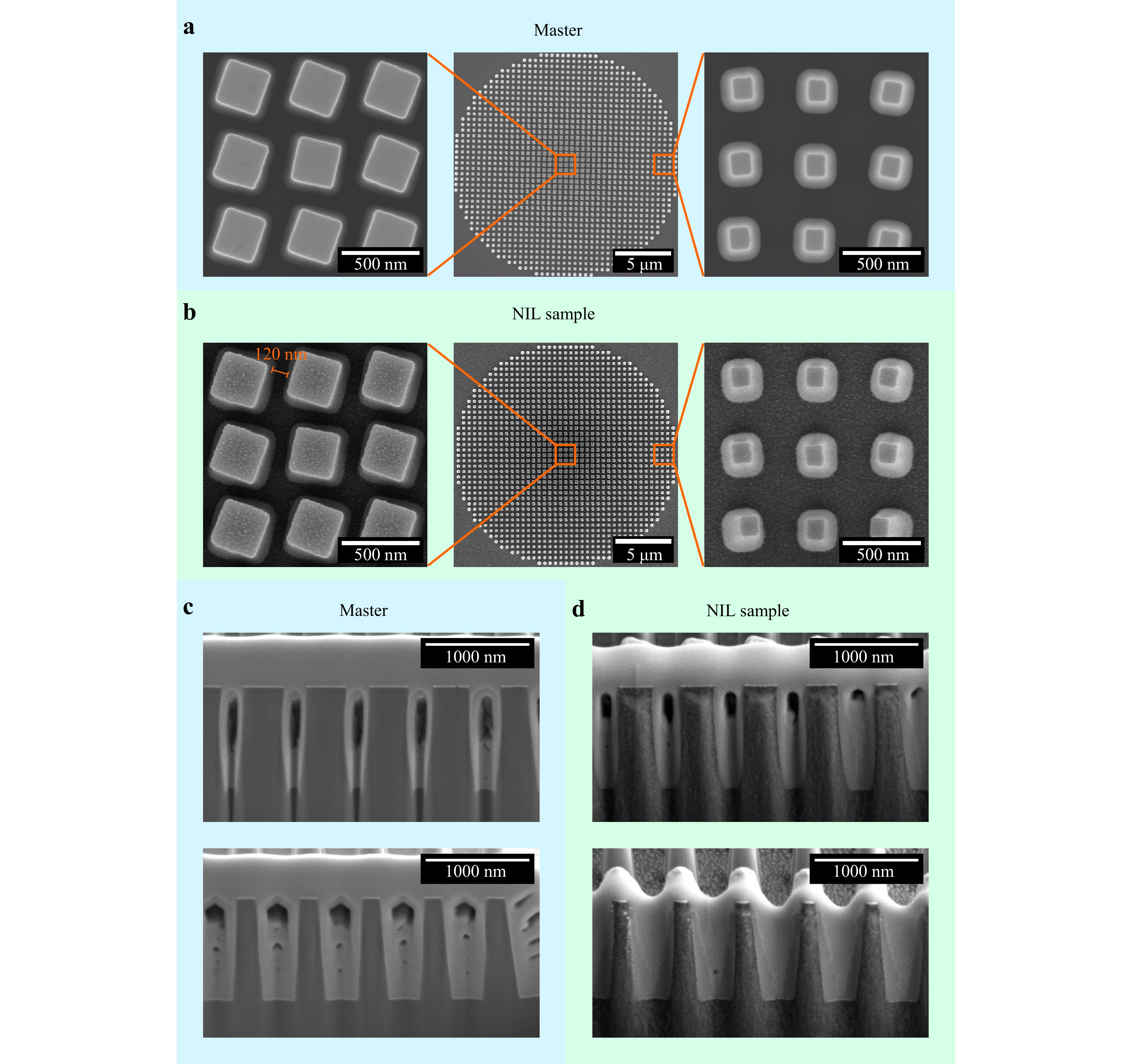
Fig. 3 SEM and FIB-SEM images of the fabricated metalens (including the master and NIL sample). a, b SEM images (top view): a Overall morphology of the metalens and detailed views of meta-atoms in the central and edge regions of the master; b corresponding top-view images of the NIL sample. The minimum structural gap (~120 nm) is labelled in the images. c, d FIB-SEM images (cross-sectional view): c Cross-sections of meta-atoms in the central and edge regions of the master; d corresponding cross-sectional images of the NIL sample.
To analyse the structural fidelity induced by each process step, we used the image analysis software ImageJ to measure the critical dimensions of the meta-atom in detail from the SEM and FIB-SEM images. Because the fabricated meta-atoms in this study had a certain sidewall tilt angle, the half-height width $ ({W}_{Half}) $, half-height length $ ({L}_{Half}) $, and height $ (H) $ of the meta-atoms were used as characteristic parameters to analyse the shrinkage rate to accurately reflect the change in their actual volume (i.e. equivalent refractive index). The specific measurements and statistical methods are described in the Materials and Methods section.
To determine the lateral shrinkage rate, front-view SEM measurements and dimensional analyses were performed on 30 meta-atoms in five different regions of the metalens. SEM images of the master mould and NIL sample with metalens numbering are presented in Figs. S7, S8, and S9 in the Supplementary Materials. The $ {W}_{Half} $, $ {L}_{Half} $, and corresponding shrinkage rate data for all 30 meta-atoms are listed in Tables S3–S5. The results showed that the lateral shrinkage rates of all meta-atoms did not exceed 5.19%. For the vertical shrinkage rate, the heights of 10 meta-atoms were measured, and their shrinkage rates were calculated (Fig. S10 and Table S6); all measured vertical shrinkage rates were below 4.87%. The statistical results of the average shrinkage rates of all meta-atoms were as follows: the average width shrinkage rate ($ {W}_{Shrinkage} $) was 2.23% ± 1.98%, the average length shrinkage rate ($ {L}_{Shrinkage} $) was 1.87% ± 1.76%, and the average height shrinkage rate ($ {H}_{Shrinkage} $) was 3.47% ± 1.38%. This indicated that the use of the working stamp material, nanoimprint photoresist, and supporting process flow detailed in Fig. S6 enables an effective high-fidelity replication of nanostructures, thereby providing a reliable basis for the high-precision fabrication of metalenses.
The designed dimensions of the meta-atoms and measured dimensions of the NIL samples are compared in Table S7. For meta-atom structures of different sizes, dimensional errors in opposite positive and negative directions were observed. This may be attributed to two processes during master mould fabrication: the optimal exposure dose and etching rate for nanostructures of different sizes are inconsistent. These errors can be effectively compensated for by modifying the design parameters of the fabrication drawings.
A measurement setup was employed to characterise the optical properties of the metalens, as shown in Fig. 4a. Fig. 4b presents the normalised in-plane (y = 0 cross-section, x-z plane) intensity distribution of the achromatic metalens at five sampled wavelengths within the 480–640 nm range, where the white dashed lines indicate the actual focal length positions corresponding to each wavelength. As clearly observed in the figure, the focal length positions remained nearly unchanged at various wavelengths, indicating the excellent achromatic focusing performance of the metalens. Fig. 4c shows the measured intensity distribution at the focal plane at the aforementioned selected wavelengths, whereas Fig. 4d presents the normalised intensity curves of the horizontal and vertical cross-sections of the focal plane. The results demonstrated that the focal spots maintained good symmetry at all wavelengths without apparent morphological distortion, confirming that the metalens possesses a stable focusing capability. Additionally, in Fig. 4e, the measured and simulated focal lengths of the metalens are compared for the five sampled wavelengths. Fig. S11 and Table S8 present the statistical data from five repeated focal length measurements. To quantitatively evaluate the achromatic performance of the metalens, we adopted the focal length standard deviation (FLSD) as the metric using the calculation method described in Materials and Methods. Within the entire designed wavelength range of 480–640 nm, the deviation between the measured and simulated values did not exceed 2 μm (<2%), the average value was 115.68 μm, and the FLSD was only 1.14 μm, indicating excellent achromatic performance.
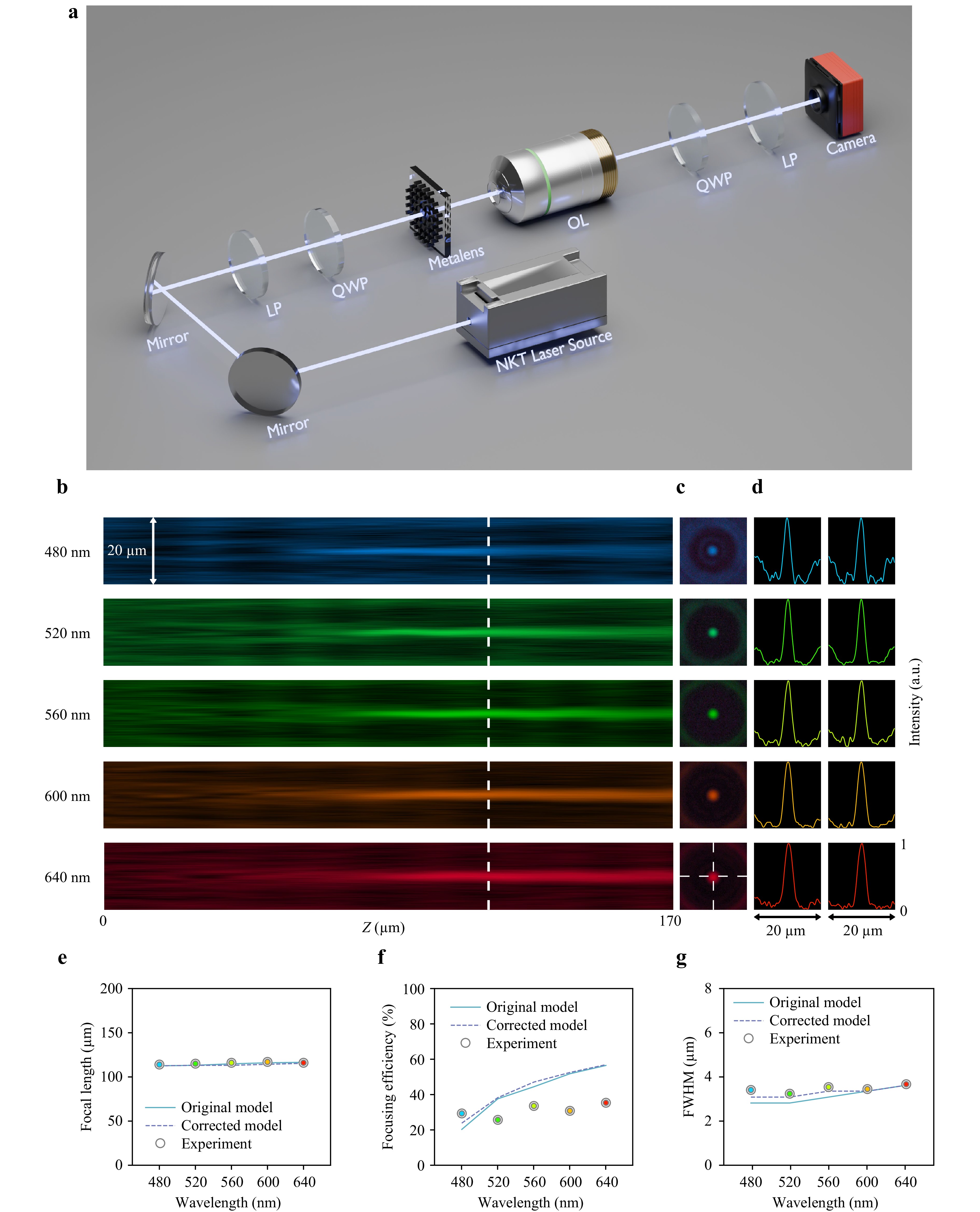
Fig. 4 Measured results of the optical properties of the achromatic metalens, particularly for the five sampled wavelengths: a Measurement setup to characterize the optical properties of the metalens. b Measured normalized intensity distribution in the x–z plane, where the white dashed lines indicate the measured focal length positions. c Measured focal plane. d Measured normalized intensity curves of the horizontal and vertical cross-sections of the focal plane. e-g Comparisons of the simulated values of the original model (metalens under ideal conditions), simulated values of the corrected model (metalens with actual fabrication errors), and experimental measurements of the fabricated metalens, including e focal lengths, f focusing efficiencies, and g FWHM.
Fig. 4f shows the measured focusing efficiency, with an average value of 30.96% across the operating wavelength range. Fig. 4g shows the measured full width at half maximum (FWHM) of the focal spot at the sampled wavelengths. The calculated FWHM ranged from 5.73λ to 7.09λ, which is close to the theoretical diffraction limit, indicating effective control over the focal spot size.
To analyse the effect of fabrication errors on optical performance, we performed a simulation using the corrected model with the measured dimension deviations (see Fig. S12). Compared with the designed value, the verticality of the sidewall had a tilt of 3° (the ideal vertical angle is 90°, whereas the actual angle was 87°); the meta-atom height ranged from 920.04 to 951.76 nm; the meta-atom size decreased by 6.03 nm at the centre and increased by 15.60 nm at the edge.
As shown in Fig. 4e and Table S2, the experimentally measured focal length and FLSD of the metalens agreed closely with the simulated values from the corrected model. The difference in the average focal length was only 0.16 μm, whereas the difference in the FLSD was 0.38 μm. Fig. 4f, g show the focusing efficiency and FWHM at different wavelengths. Although the measured focusing efficiency was still lower than the value simulated with the corrected model, their variation trends were consistent, i.e. the focusing efficiency increased with increasing wavelength. The FWHM of the corrected models increased slightly at several short wavelengths compared with the original model, which was closer to the experimental values. However, it remained near the diffraction limit of 5.97λ, indicating excellent focusing performance.
Generally, the simulation results of the original and corrected models showed no significant differences, indicating that our metalens design has a high error tolerance. The high consistency between the experimental and corrected simulated focal length and FWHM values confirmed the reliability of the experimental results. In addition, the effects of different dimensional and measurement errors on the focusing efficiency were analysed through simulation and are listed in Tables S9 and S10. The simulation results demonstrated that the lower focusing efficiency observed in the experiments can be attributed to measurement errors rather than fabrication-induced dimensional errors.
-
In this study, a novel nanoimprint photoresist with high refractive index (1.92–1.97), high transmittance (>99%), and low shrinkage rate (≤5.19%) was used as the meta-atom material. Based on this photoresist, an achromatic metalens was designed via a combination of propagation and geometric phase principles and fabricated using one-step NIL. Furthermore, using a fast UV-curable working stamp resin, the entire processing of the metalens was completed within 15 min. Owing to the low shrinkage of the photoresist, the dimensional deviation of the fabricated meta-atom structures was only 0%–5.19% relative to the NIL master. High-precision fabrication endowed the metalens with excellent focusing and achromatic performance: in the 480–640 nm wavelength range, the normalized intensity curves of the focal plane were highly consistent with the designed ones, and the measured focal length deviation for different wavelengths was only <2%. In conclusion, the novel photoresist and UV-curable working stamp materials enable low-cost, high-efficiency, and high-precision NIL fabrication of achromatic metalenses. It has substantial application potential in compact imaging, augmented reality displays, and integrated photonics. Future research could develop larger-aperture metalenses and achieve wafer-level large-scale production via large-size master fabrication45,46.
-
The nanoimprint photoresist was prepared as follows: First, a silane solution and an ethyl acetate solution containing TiO2 nanoparticles were mixed at a weight ratio of 1:12.8. Subsequently, the resulting silane-nanoparticle solution was added to a mixture of methacryl-functionalized silane, a transparent acrylate polymer, and a photosensitizer. After ultrasonic treatment to homogenise the dispersion, the prepared nanoimprint photoresist was filtered through Teflon filters (pore size: 0.22 μm). The mass fraction of TiO2 nanoparticles in the hybrid system was 60%.
-
As shown in Fig. S6a, first, an EBL system (JBX-9500FS, JEOL) and a photoresist (ZEP520) were used to fabricate the inverse nanopore patterns. Subsequently, a 30 nm-thick Cr film was deposited via electron beam evaporation, and a lift-off process was employed to remove the photoresist from the unexposed areas, leaving a Cr hard mask pattern consistent with the meta-atom structure on the silicon wafer substrate. Next, an ICP etching system (PlasmaPro 100 Cobra 180, OXFORD) and a mixed gas of SF6 and CHF3 were used to etch and form the desired silicon meta-atom structure morphology. Finally, the residual Cr etching mask was removed via wet etching to yield the master. The master was treated with a vaporised fluorine solution to render it hydrophobic to reduce surface adhesion of the master and facilitate the subsequent demoulding process.
-
As shown in Fig. S6b, first, a UV-curable working stamp resin (WSA08, OuGuangXin Technology) was drop-coated onto the master surface. Subsequently, a polyethylene terephthalate (PET) flexible film was attached to the surface of the glass cover plate of the NIL apparatus (GL4 R&D, GermanLitho). The equipment could automatically execute the following process steps: First, the glass cover plate was controlled to descend slowly, which enabled the PET flexible film to gradually contact WSA08 until full lamination was achieved. Subsequently, a UV LED lamp with a wavelength of 365 nm and power of 300 W was used for exposure, which enabled WSA08 to be fully cured in only 3 min. Finally, the PET flexible film with cured WSA08 was peeled off from the master mould. Through this process, the inverse metalens pattern was transferred onto the surface of WSA08, thus completing the fabrication of the working mould. The entire processing of the working stamp was completed within 5 min.
-
This is shown in Fig. S6c. First, the quartz glass substrate surface was treated with O2 plasma (power: 500 W, duration: 10 min) to enhance its adhesion to the imprint photoresist. After the treatment, a tackifier (P101, OuGuangXin Technology) was spin-coated onto the substrate surface at a rotational speed of 1,000 rpm, followed by heating on a hot plate at 120 °C for 1 min. Subsequently, the nanoimprint photoresist (O2190) was spin-coated onto the substrate surface at 1,000 rpm, heated on a hot plate at 80 °C for 30 s, and then the NIL system (UniPrinter, GermanLitho) was used to automatically complete the imprinting, exposure, and demoulding processes. The spin-coating method was used to ensure uniformity of the residual layer thickness after imprinting. The specific process parameters were as follows: a pressure of 10 WPa, imprinting speed of 0.3 mm/s, exposure lamp (wavelength: 365 nm, power: 300 W) with an exposure time of 30 s, and demoulding speed of 0.2 mm/s. The entire NIL process can be completed within 5 min, and the working stamp based on WSA08 can be reused multiple times, providing a guarantee for low-cost large-scale production of metalenses.
-
To evaluate the achromatic performance of the metalens quantitatively, we adopted the FLSD as the evaluation index, defined as follows:
Let $ {f}_{i} $ be the focal length at the $ i $-th wavelength within the operating band, and the average focal length $ \overline{f} $ is
$$ \overline{f}=\frac{1}{N}\sum\limits_{i=1}^{N}{f}_{i} $$ (2) The focal length standard deviation $ {\sigma }_{f} $ is
$$ {\sigma }_{f}=\sqrt{\frac{1}{N}\sum\limits_{i=1}^{N}({f}_{i}-\overline{f}{)}^{2}} $$ (3) where $ N $ is the total number of measured wavelengths. A smaller FLSD indicates smaller focal-length fluctuations at different wavelengths and superior achromatic performance of the metalens.
-
First, a database of the corresponding relationships between the geometric parameters of meta-atoms and the optical properties (including phase, amplitude, and group delay) was established through parametric scanning. During the meta-atom arrangement process, the particle swarm optimization (PSO) algorithm was used to screen suitable meta-atoms according to the group delay requirement at the target position. Subsequently, by adjusting the rotation angle of the meta-atoms, their geometric phase was used to compensate for the phase difference. The achromatic metalens for 480–640 nm wavelength range was designed with $ \text{Si}{\mathrm{O}}_{2} $ as the substrate and a high-refractive-index nanoimprint photoresist (O2190) as the meta-atom material. To systematically evaluate the focusing performance of the metalens, we employed the finite-difference time-domain method and selected five wavelength samples were selected within the wavelength range of 480–640 nm for the focal-field analysis.
-
The half-height width $ ({W}_{\rm{Half}}) $, half-height length $ ({L}_{\rm{Half}}) $, and height of the meta-atoms in the master and NIL sample were used as evaluation indicators to analyse the dimensional changes (i.e. shrinkage rate). Here, $ {W}_{\rm{Half}} $ is defined as the average of the top width $ ({W}_{\rm{Top}}) $ and bottom width $ ({W}_{\rm{Bottom}}) $ of the meta-atom, and $ {L}_{\rm{Half}} $ is defined as the average of the top length $ ({L}_{\rm{Top}}) $ and bottom width $ ({L}_{\rm{Bottom}}) $:
$$ \begin{cases} {W}_{Shrinkage}=\dfrac{{W}_{Half,Master}-{W}_{Half,NIL}}{{W}_{Half,Master}}\times 100\%\\ {L}_{Shrinkage}=\dfrac{{L}_{Half,Master}-{L}_{Half,NIL}}{{L}_{Half,Master}}\times 100\%\\ {H}_{Shrinkage}=\dfrac{{H}_{Master}-{H}_{NIL}}{{H}_{Master}}\times 100\% \end{cases} $$ (4) where $ {{W}}_{\text{Shrinkage}} $, $ {{L}}_{\text{Shrinkage}} $, and $ {{H}}_{\text{Shrinkage}} $ represent the shrinkage rates of the width, length, and height of the meta-atom, respectively.
For the lateral shrinkage rate calculation, first, 30 meta-atoms at five different positions on the metalens were characterised using front-view SEM, and each meta-atom in the images was numbered, corresponding to Fig. S7, S8, and S9. Thereafter, $ {{W}}_{\text{Top}} $, $ {{W}}_{\text{Bottom}} $, $ {{L}}_{\text{Top}} $, and $ {{L}}_{\text{Bottom}} $ of each meta-atom were measured individually using ImageJ, $ {{W}}_{\text{Half}} $ and $ {{L}}_{\text{Half}} $ were calculated, and the shrinkage rate of each meta-atom was further computed. The relevant data are compiled in Tables S3, S4, and S5 in the Supplementary Materials. Finally, the arithmetic mean and standard deviation of the width and length shrinkage rates were calculated for all 30 meta-atoms.
To calculate the height shrinkage rate, first, we captured cross-sectional images of meta-atoms with larger and smaller sizes at the central and edge positions of the lens using FIB-SEM. The heights of all meta-atoms were then measured, and the average height was taken as the final height of the sample (see Table S6).
-
A measurement setup was employed to characterise the optical properties of the metalens, as shown in Fig. 4a. The light source used in the experiment was an NKT SuperK EXTREME laser, which emits linearly polarised laser light. This laser light was converted into left-handed circularly polarised light using an LP and QWP before reaching the metalens sample. The focused spot was captured using an imaging system consisting of a 40× microscopic objective lens (OL, Nikon) and CCD camera (Thorlabs). The second set of QWP and LP combinations in the system was used to extract the optical field of the target polarisation, eliminate interference, and enable the accurate measurement of the target optical field.
In this study, focusing efficiency was defined as the ratio of the transmitted light power within the effective region of the focal spot to the incident light power within a circular area with the same effective aperture as the metalens at the target operating wavelength. The effective region of the focal spot was defined as a circular area with a radius of three times the FWHM (3×FWHM) of the focal spot, ensuring that most of the focused light energy is included in the calculation. The incident light power was the incident light power within a circular area, which was consistent with the effective aperture size of the metalens. This definition follows the general characterisation standards in this field and has good universality and comparability47.
The effective aperture of the metalens in this study was only 20 μm. Its small size makes it impossible for commercial power meters to directly and accurately measure focused light power. Therefore, the experiment adopted the CCD grayscale integration method to achieve quantitative characterisation of light power within the working range, where the CCD has a linear response and no overexposure, and spot images of the incident light and the focused focal spot are collected. The total grayscale value of all the pixels in the effective region was calculated to replace the light power equivalently, thereby completing the quantitative calculation of the focusing efficiency and achieving high-precision testing of the focusing efficiency of small-sized metalenses.
-
This study was supported by the National Natural Science Foundation of China (Grant No. 62575023).
Scalable nanoimprint manufacturing of achromatic metalenses based on a high-refractive-index and low-shrinkage photoresist
- Light: Advanced Manufacturing , Article number: 105 (2026)
- Received: 20 November 2025
- Revised: 16 June 2026
- Accepted: 22 June 2026 Published online: 07 September 2026
doi: https://doi.org/10.37188/lam.2026.105
Abstract: An achromatic metalens (480–640 nm) was designed via integrating propagation and geometric phase principles and fabricated using one-step nanoimprint lithography (NIL). A novel nanoimprint photoresist was used, which not only has a high refractive index (1.92–1.97) and high transmittance (>99%) but also exhibits low shrinkage (≤5.19%). This low shrinkage results in small dimensional deviations of the meta-atoms relative to the NIL master. The working stamp was fabricated in 10 min using an ultraviolet-curable material. This process is much faster than polydimethylsiloxane-based alternatives, which require several hours of thermal curing. Owing to its high fabrication accuracy, the metalens exhibited excellent focusing and achromatic performance, with a wavelength-dependent focal-length deviation of <2%. This study has provided a potential route for the high-precision, high-efficiency, and large-scale production of achromatic metalenses and other nano/micro-optical devices.
Research Summary
Metalenses: Scalable fabrication by nanoimprint lithography
Metalenses offer a compact alternative to conventional optics, but their widespread adoption has been hindered by the difficulty of manufacturing nanoscale structures with high precision and at low cost. Researchers have developed a scalable nanoimprint lithography approach for producing visible-light achromatic metalenses. The method combines a high-refractive-index photoresist with low shrinkage and a rapidly fabricated UV-curable working stamp. Together, these advances enable accurate replication of nanoscale features while improving manufacturing efficiency. The resulting metalenses maintain nearly constant focal lengths across a broad visible wavelength range, demonstrating achromatic performance. By reducing fabrication complexity while maintaining fabrication accuracy, this approach could support the large-scale production of metalenses for applications including compact imaging systems, augmented-reality displays and integrated photonic devices.
Rights and permissions
Open Access This article is licensed under a Creative Commons Attribution 4.0 International License, which permits use, sharing, adaptation, distribution and reproduction in any medium or format, as long as you give appropriate credit to the original author(s) and the source, provide a link to the Creative Commons license, and indicate if changes were made. The images or other third party material in this article are included in the article′s Creative Commons license, unless indicated otherwise in a credit line to the material. If material is not included in the article′s Creative Commons license and your intended use is not permitted by statutory regulation or exceeds the permitted use, you will need to obtain permission directly from the copyright holder. To view a copy of this license, visit http://creativecommons.org/licenses/by/4.0/.

 DownLoad: