



-
Integrated circuits (ICs) are the core components of modern electronic devices, driving key technological innovations across numerous fields, including artificial intelligence1, 2, wireless communications3-5, virtual reality6, 7, the Internet of Things8-10, and biomedicine11-14. Driven by Moore's Law15, the semiconductor industry continuously scales down feature sizes to achieve higher transistor density. This trend highlights the critical role of lithography, the core patterning technique used to transfer circuit designs from mask to wafer16, 17. To meet the strict resolution requirements of nanostructure fabrication, lithography techniques and related molecular strategies must continuously evolve18.
However, as technology nodes advance to 7 nm and beyond, conventional lithography faces severe physical, equipment, and process limitations. Physically, the Rayleigh criterion dictates that diffraction effects limit resolution when feature dimensions shrink below the exposure wavelength19. This effect directly causes blurred edges and poor pattern fidelity. On the equipment side, optical systems face performance bottlenecks. Additionally, stage positioning errors during high-speed motion degrade critical dimension uniformity and increase overlay error20, 21. On the process level, stochastic effects have emerged as a primary obstacle, particularly in extreme ultraviolet (EUV) lithography. Specifically, photon shot noise induced variability and stochastic photoresist fluctuations severely degrade the local critical dimension uniformity (CDU). These variations directly cause critical defects, such as line breaks and bridges22-24. Collectively, these bottlenecks narrow the process window and limit yield improvement.
To overcome these lithographic limitations, the industry has turned its attention to curvilinear mask technology25-27. This technology uses pattern and software innovations to bypass traditional physical limits. Unlike conventional masks, curvilinear masks offer superior fidelity in complex regions with high curvature and corners. They effectively suppress imaging errors. They also significantly reduce line width roughness (LWR) and edge placement error (EPE). Furthermore, these masks reduce critical defects and enable more compact design rules. As equipment and process capabilities reach their physical limits, curvilinear masks become essential. They provide a practical way for both deep ultraviolet (DUV) and EUV lithography to expand the process window and improve manufacturing yield.
This paper provides an overview of curvilinear mask technology in integrated circuit lithography. The generation mechanism of curvilinear masks is briefly introduced, followed by their advantages for manufacturing and design. The paper then presents a survey of the research progress in the key enabling technologies required for its adoption. Building on this foundation, the specific application scenarios of curvilinear masks and the current challenges impeding their high-volume manufacturing are systematically analyzed. The paper concludes by discussing future directions.
-
Curvilinear masks originate from inverse lithography technology (ILT), a computational method that formulates mask design as an inverse problem28-30. ILT computationally solves for an optimal mask to maximize pattern fidelity and expand the process window. By exploring a vast solution space, this approach yields complex, non-intuitive, and inherently curvilinear patterns that pre-compensate for optical distortions.
The ILT framework recasts mask design as a large-scale optimization problem. The complete lithography process is represented by a forward operator $ f $, which models the transformation from a mask pattern $ \psi $ to the final wafer pattern $ \omega $:
$$ \omega = f(\psi) $$ (1) This operator is composed of a spatial imaging model that calculates the aerial image intensity on the wafer and a photoresist model that converts this intensity into the final wafer pattern.
The goal is to find an optimal mask $ \psi^* $, by minimizing a cost function $ F(\psi) $, which measures the deviation between the simulated wafer pattern and a desired target $ \phi $. Because a direct analytical solution is not feasible, the problem is addressed through numerical optimization. The cost function is typically the squared L2 error, and the optimal mask is the one that minimizes this cost:
$$ F(\psi) = \| f(\psi) - \Phi \|_2^2 $$ (2) $$ \psi^* = \arg \min F(\psi) $$ (3) Various gradient-based algorithms are employed to iteratively solve this minimization problem. These solvers adjust the mask pattern on a pixelated grid, guided by the cost function’s gradient, until the solution converges on the final free-form, curvilinear mask pattern.
-
On the manufacturing side, curvilinear technology addresses lithography bottlenecks at advanced nodes from two key dimensions: lithographic performance and manufacturability. In terms of lithographic performance, curvilinear techniques significantly widen the process window, enhance pattern fidelity, and reduce sensitivity to mask errors. In 2009, a collaborative study by Samsung and Luminescent31 demonstrated the efficiency of curvilinear ILT masks for contact hole arrays. As quantified in Fig. 1a, optimizing sub-resolution assist features (SRAFs) into simplified curvilinear patterns achieves a 20% to 100% enhancement in the depth of focus (DOF) compared to conventional optical proximity correction (OPC). With technological advancements, experimental results from Micron36 on random contact layers indicated that full-chip curvilinear ILT achieved a process window improvement of over 100%. Further investigations on dynamic random access memory (DRAM) contact holes32 corroborate this trend. As illustrated by the process windows in Fig. 1b, a full curvilinear ILT solution extends the usable DOF by approximately 85%. It also maintains a significantly tighter process variation (PV) band under varying defocus conditions (0, 60, and 90 nm), thereby ensuring greater manufacturing robustness.
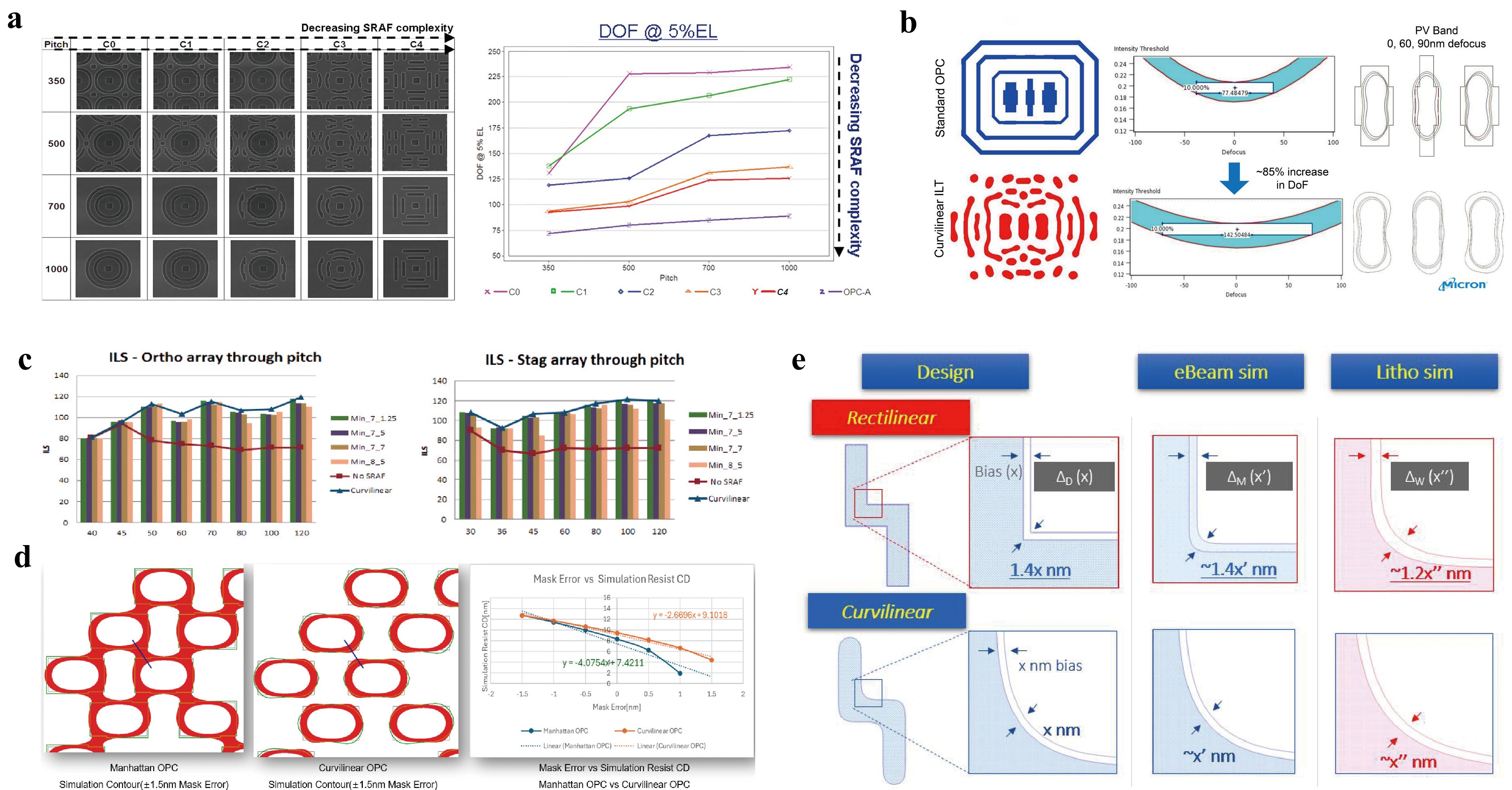
Fig. 1 Simulation and experimental verification of curvilinear masks. a SEM images and DOF performance for through-pitch ILT contact arrays31. Bar charts compare the depth of focus between simplified curvilinear ILT and conventional OPC across different pitches. b Process window and PV band comparison32. Plotted process windows and overlay contours show the physical variance of PV bands under varying defocus conditions. c ILS comparison for via arrays33. ILS values plotted against pitch dimensions compare the imaging performance of various SRAF configurations. d MEEF analysis for logic via layers34. Scatter plots trace the simulated resist CD response to applied mask errors for both OPC methods. e Impact of uniform mask bias35. Biased contours overlaid onto original targets show the spatial edge displacement at corners versus smooth curves.
Furthermore, beyond the macroscopic process window, curvilinear mask technology fundamentally improves localized imaging metrics. For instance, evaluations of dense via array test patterns33 reveal the specific advantages of curvilinear SRAFs. Fig. 1c shows that these curvilinear patterns consistently yield higher Image Log Slope (ILS) values across diverse pitches than conventional rule-based designs. This elevated ILS directly translates to sharper image contrast and reduced edge placement errors. Concurrently, by eliminating physically unstable sharp corners, curvilinear masks markedly reduce the mask error enhancement factor (MEEF). A 2022 study37 confirmed that the MEEF of smooth curvilinear test patterns improved by approximately 28% over their Manhattan counterparts. This suppression of error amplification is particularly crucial for high-numerical-aperture (High-NA) EUV lithography. ASML analyzed logic via layers to evaluate this effect34. As demonstrated by the linear fit in Fig. 1d, curvilinear OPC exhibits a substantially lower slope for mask error versus simulated resist critical dimension(CD). This visually confirms its superior capability to prevent mask CD variations from translating into massive wafer CD deviations.
During e-beam mask writing, the 90-degree corners of Manhattan patterns are highly sensitive to dose fluctuations, representing the most unstable features in fabrication. Curvilinear technology enhances mask manufacturability by eliminating these sharp corners to mitigate this instability. A study by Pang et al.38 demonstrated that under identical processes, curvilinear patterns reduce the contour variation band by approximately 20%, with a narrower and more normal distribution of variation. Moreover, curvilinear masks offer inherently higher predictability against systematic process variations like uniform mask bias. Fig. 1e physically illustrates this geometric advantage. Applying bias to Manhattan patterns triggers a severe and non-linear error amplification at the 90-degree corners, typically yielding a 1.4-fold displacement. Conversely, the same bias applied to curvilinear patterns transfers uniformly along the contour35. This uniform stress distribution minimizes localized CD distortions to ensure a highly reliable pattern transfer process.
-
Introducing curvilinear patterns into standard cells and tight-pitch metal layers breaks traditional layout constraints, enabling higher transistor density and significant area reduction. In a standard cell for the 14A technology node, a curvilinear layout is considerably more compact than a conventional one-dimensional (1D) Manhattan design. According to research by IMEC, this optimization reduces the standard cell height from 5T to 4T at the 1.4 nm node, directly yielding a 20% area scaling39. This area advantage stems from improved routing efficiency, as curvilinear routing enables all connections to be completed efficiently within the M0 layer, whereas Manhattan designs require higher-level metals and additional vias to overcome routing congestion39. As detailed in Fig. 2a, 1D Manhattan designs restrict source-to-gate connections to strictly orthogonal paths, necessitating extra layers, whereas curvilinear patterns establish direct connections within the M0 layer.
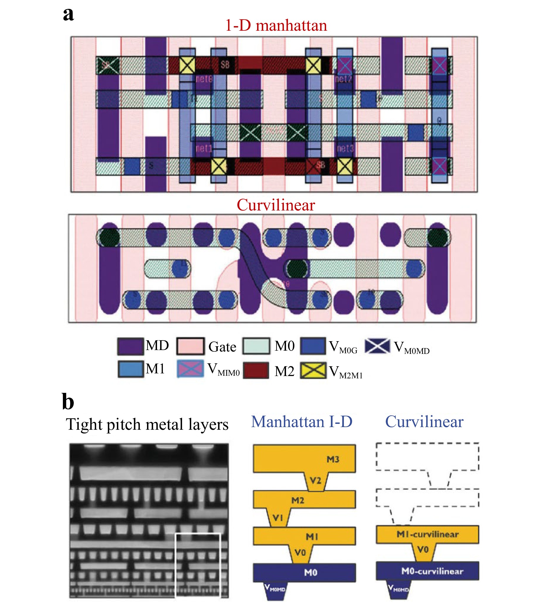
Fig. 2 Advantages of curvilinear design. a Comparison of routing efficiency between 1D Manhattan and curvilinear designs39. Curvilinear patterns complete source-to-gate connections entirely within the M0 layer, avoiding the extra layers required by Manhattan's strictly orthogonal constraints. b Vertical stack reduction showing the elimination of upper metal layers via curvilinear design39. This specifically highlights the removal of higher-level metals (e.g., M2, M3) and vias (e.g., V1, V2) to reduce manufacturing complexity and cost
This design optimization also yields concomitant advantages in manufacturing and performance. By efficiently utilizing bottom-level metals, curvilinear design eliminates the need for higher metal layers such as M2 and M3 (Fig. 2b), which illustrates the vertical stack reduction achieved by removing these upper metals and their associated vias (e.g., V1, V2), leading to a 7% reduction in wafer cost, a 5% shorter manufacturing cycle, and a 7% simplification of process steps. Concurrently, the shorter, more direct connection paths reduce parasitic RC delay by avoiding extra vias, ultimately resulting in an approximately 5% performance improvement39.
-
Curvilinear mask technology involves a highly integrated, multi-stage workflow. This review categorizes the key enabling technologies by their deployment across the layout, mask, and wafer dimensions, as shown in Fig. 3. The following sections will discuss the research progress, advantages, and limitations within the five core stages: curvilinear design, OPC solution, mask enablement, mask writer, and wafer metrology.
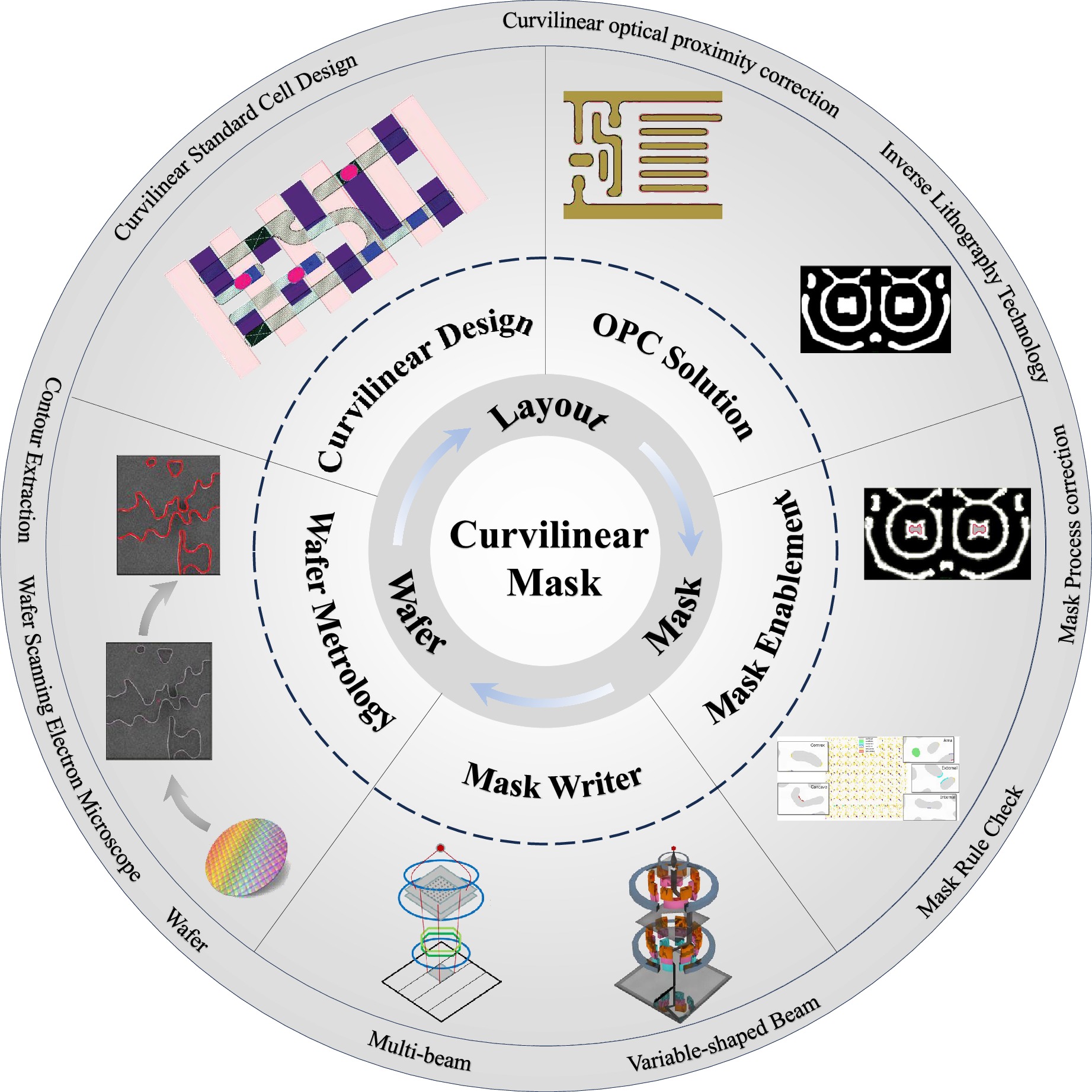
Fig. 3 Overview of curvilinear mask technology. This diagram delineates the integrated manufacturing ecosystem across the layout, mask, and wafer dimensions. It maps five core stages to illustrate the continuous process and data flow required for technology deployment. These stages comprise curvilinear design, OPC solution, mask enablement, mask writer, and wafer metrology39-44.
-
The pursuit of higher transistor density led to restrictive one-dimensional (1D) Manhattan standard cell layouts, which created severe intra-cell routing congestion. This congestion necessitates extra metal layers and vias, increasing both manufacturing costs and parasitic parameters that degrade performance. Curvilinear design resolves this challenge by introducing shorter, non-orthogonal connections, enabling continued Power, Performance, Area, and Cost (PPAC) optimization without increasing cell area.
Early research from IMEC identified curvilinear routing as a key solution for congestion in IN5 standard cells, while also noting ecosystem challenges such as electronic design automation (EDA) tool support and physical verification45. IMEC employed a curvilinear MINT layer design in a D-flipflop standard cell46. As depicted in Fig. 4a, non-orthogonal metal tracks circumvent internal pin obstacles to establish direct electrical connections. This routing strategy effectively alleviates local interconnect congestion. An EUV single exposure wafer tape-out subsequently confirmed the manufacturability of these curvilinear patterns at a 32 nm pitch. More recently, a hybrid strategy combining 1D Manhattan routing with curvilinear connections was proposed, using Voronoi diagrams and A* search algorithms to design a flip-flop standard cell47. Fig. 4b illustrates the layout evolution from strictly orthogonal Manhattan routing to full curvilinear intra-cell routing. This comparison demonstrates that curvilinear paths connect node pairs across the shortest physical distances. This structural optimization actively reduces total metal length, decreases the number of vias, and eliminates the need for extra metal layers. To guide industrial adoption, IMEC has proposed a phased roadmap, progressing from restricted use in specific areas to partial integration within standard cells, and ultimately to full-chip, free-form design48.
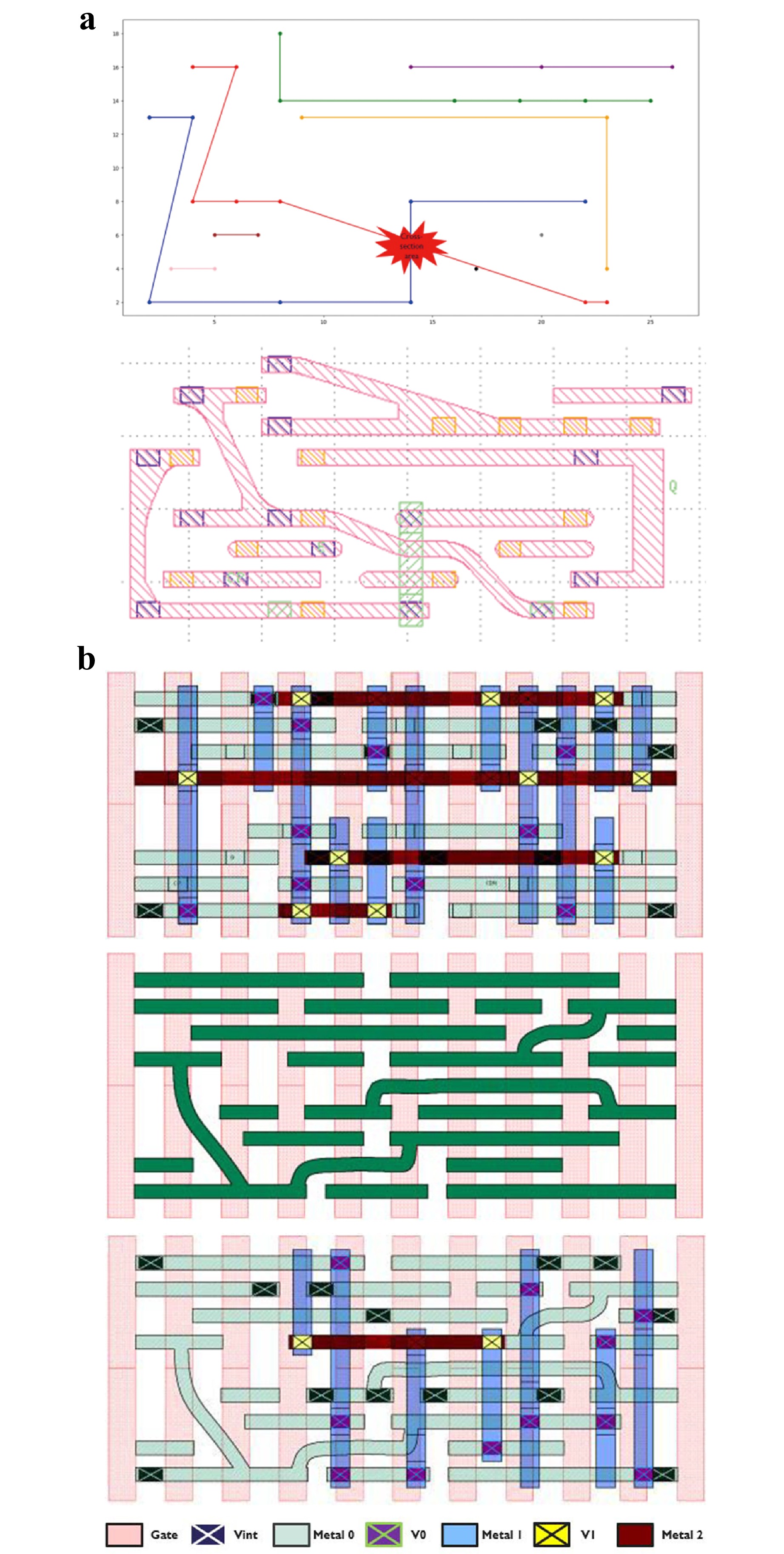
Fig. 4 Curvilinear layout design strategies. a Pin connection generation and MINT layer optimization46. Non-orthogonal paths circumvent adjacent pins to resolve local routing congestion. b Comparison of Manhattan routing, curvilinear Metal 0 layer, and full curvilinear intra-cell routing for flip-flop standard cells47. This structural comparison confirms that curvilinear tracks minimize connection distances and eliminate additional via layers.
-
The advent of curvilinear masks necessitates new approaches to OPC, leading to two primary technical paths. The first is ILT, which pixelates the mask and uses global optimization to generate inherently curvilinear patterns. The second is curvilinear OPC, which adapts traditional edge-based correction into a parametric methodology that balances computational efficiency with lithographic performance. This section reviews the research progress for both solutions.
-
Driven by specific algorithmic and hardware developments, the evolution of ILT progressed from foundational academic concepts in the 1980s49 to full-chip commercial solutions. Early research established the core mathematical frameworks focusing on level-set methods50-52, pixelated phase-shifting53, and gradient-based or regularization algorithms54-63. However, since high computational cost remained a primary challenge, the industry shifted toward hardware-software co-design. One significant approach utilized a frequency-domain solver paired with a dedicated GPU platform to enable full-chip curvilinear ILT without partitioning and stitching errors36, 64.
Recently, artificial intelligence (AI) accelerated the ILT workflow along three main technical trajectories. First, AI serves as an accelerator for traditional physical iterative processes, where deep convolutional neural networks rapidly generate initial SRAF layouts65. Second, researchers developed end-to-end models such as generative adversarial networks (GANs)66, variational autoencoders (VAEs)67, and graph convolutional networks (GCNs)68 to directly map target patterns to optimal masks and bypass conventional iterative optimization. Third, to address the limited physical interpretability of conventional deep learning, model-driven deep learning emerged as a practical solution that directly embeds lithographic physical models into the network architecture. Implementations including the model-driven convolutional neural network (MCNN)69, dual-channel model-driven deep learning (DMDL)70, and partially coherent illumination model-informed deep learning (PCI-MIDL)71 ensure both high computational efficiency and strict physical compliance. Table 1 summarizes the key research progress in ILT from early commercialization to recent AI innovations.
Research Direction Core Content References Early commercialization and theoretical basis Theoretical foundations, level-set methods, and pixelated phase-shifting masks. 49-53 Fundamental optimization algorithms Gradient-based methods and regularization frameworks for inverse optimization. 54-63 Hardware-software co-design Frequency-domain solvers on GPU platforms enabling full-chip ILT without stitching errors. 36, 64 AI-accelerated iterative processes CNN-based rapid pre-generation of initial SRAF layouts. 65 End-to-end AI models Direct pattern-to-mask mapping utilizing GANs, VAEs, and GCNs. 66-68 Model-driven deep learning Physics-embedded network architectures (e.g., MCNN, DMDL, PCI-MIDL) ensuring physical
interpretability and compliance.69-71 Table 1. Summary of Research Progress in Inverse Lithography Technology
-
Curvilinear OPC evolves from the mature and controllable frameworks of traditional OPC72, 73 by adopting a parametric methodology. This transition achieves lithographic fidelity comparable to inverse lithography technology while drastically mitigating computational overhead. Current research in this domain converges on three primary trajectories: mathematical refinement of curve representations, AI-driven workflow acceleration, and pattern-aware targeted deployment.
At the foundational level, representations are mathematically refined to optimize the trade-off between imaging fidelity and data volume. As detailed in Fig. 5a, fundamental parametric methods optimize cubic Bézier curves by displacing the vertices of a base polygon74. This geometric manipulation overcomes mask rule check (MRC) limitations in dense regions. Beyond this traditional fitting, dimensionality reduction techniques map two-dimensional (2D) mask boundaries into 1D tangent angle-arc length (TAAL) functions. This simplifies control point selection and movement trajectories76. Moreover, a demand-driven dynamic framework replaces uniform sampling. It inserts control points only in critical regions, significantly improving resource allocation efficiency77. To address data explosion in high-volume manufacturing, B-spline formats are integrated with analytical MEEF matrices. This facilitates substantial data compression while preserving complex SRAFs78.
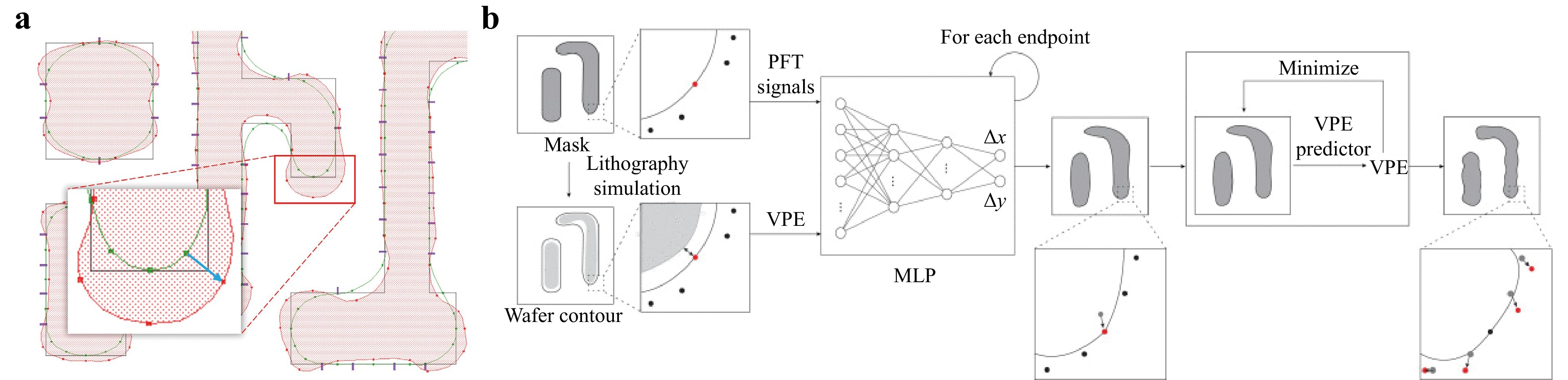
Fig. 5 Curvilinear OPC approaches. a Parametric curvilinear OPC based on vertex movement74. The optimization adjusts base polygon vertices to manipulate cubic Bézier curves, ensuring strict adherence to MRC constraints. b Machine learning-guided curvilinear OPC workflow75. An MLP predicts endpoint shifts while a GCN optimizes intermediate control points. This dual-model architecture rapidly minimizes placement errors without exhaustive heuristic iterations.
Regarding computational efficiency, integrating machine learning (ML) and hybrid workflows has emerged as the primary solution to minimize turnaround time. Decoupled strategies partition the optimization task. They reserve the curvilinear engine for main features while using fast ILT for initial SRAF generation79, 80. Furthermore, predictive ML models such as graph convolutional networks and multilayer perceptrons (MLPs) are replacing heuristic iterations75. Fig. 5b illustrates this dual-model architecture. An MLP predicts the displacement of curve endpoints, while a GCN optimizes intermediate control points. By directly estimating optimal locations through vertex placement error (VPE) metrics, this network shrinks the optimization cycle without exhaustive heuristic iterations.
Beyond algorithmic and computational enhancements, the practical implementation of curvilinear OPC focuses on pattern-aware targeted deployment rather than universal full-chip coverage. Extensive evaluations in High-NA EUV environments indicate that 1D patterns show marginal gains. Conversely, highly complex 2D layouts exhibit notable process window enlargements34. To translate this physical insight into a viable manufacturing strategy, the industry utilizes ML-assisted pattern selection to isolate lithography-sensitive 2D arrays. Applied specifically to random DRAM contacts, this targeted approach ensures rapid convergence and delivers transformative improvements, including over a 33% enhancement in depth of focus81. This deployment paradigm maximizes manufacturing yield for challenging geometries while strictly managing computational and data storage costs. Table 2 summarizes the key research achievements in curvilinear OPC.
Research Direction Core Content References Mathematical refinement of representations Evolution of curve-based optimization using native parametric forms, dimensionality reduction,
and dynamic sampling to balance fidelity and data volume.74, 76-78 AI-driven workflow acceleration Minimization of turnaround time through decoupled optimization pipelines and predictive models
for intelligent vertex displacement estimation.75, 79, 80 Pattern-aware targeted deployment Paradigm shift toward selective optimization based on pattern dependency, focusing curvilinear
resources on lithography-sensitive 2D layouts.34, 81 Table 2. Summary of Research Progress in Curvilinear Optical Proximity Correction
-
Ensuring the manufacturability of an ideal curvilinear OPC pattern requires a workflow comprising two critical stages. First, mask process correction (MPC) pre-compensates for systematic distortions introduced across the entire mask manufacturing flow. Second, a dedicated curvilinear mask rule check (CLMRC) verifies that the geometries comply with manufacturing limits. This section reviews the technological advancements in both areas.
-
MPC represents a systematic layout modulation technique that pre-compensates for inherent non-linear process biases. By modeling physical signatures of e-beam writing, resist development, and etching, MPC applies inverse compensation to ensure the fabricated mask precisely aligns with the post-OPC target. Conventional MPC algorithms, designed for Manhattan patterns, disrupt the inherent smoothness of curves by creating sharp vertices, making dedicated curvilinear MPC (CLMPC) essential for the curvilinear ecosystem.
Algorithmic advances in CLMPC have focused on enhancing efficiency and fidelity. To improve runtime, curvature-based fragmentation (CBF) intelligently adapts segmentation density, shortening MPC runtime by 45%82. For high-curvature regions, shape-modulated MPC reduces curvature error83, while an enhanced flow operating directly on Bézier curves avoids piecewise linear (PWL) conversion errors, reducing final mask error by up to 20%79. To address the limitations of shape-only corrections, a dual-layer geometric modulation method co-optimizes fidelity and contrast without altering dose by using two overlapping layers and dual PID controllers (Fig. 6a)85.
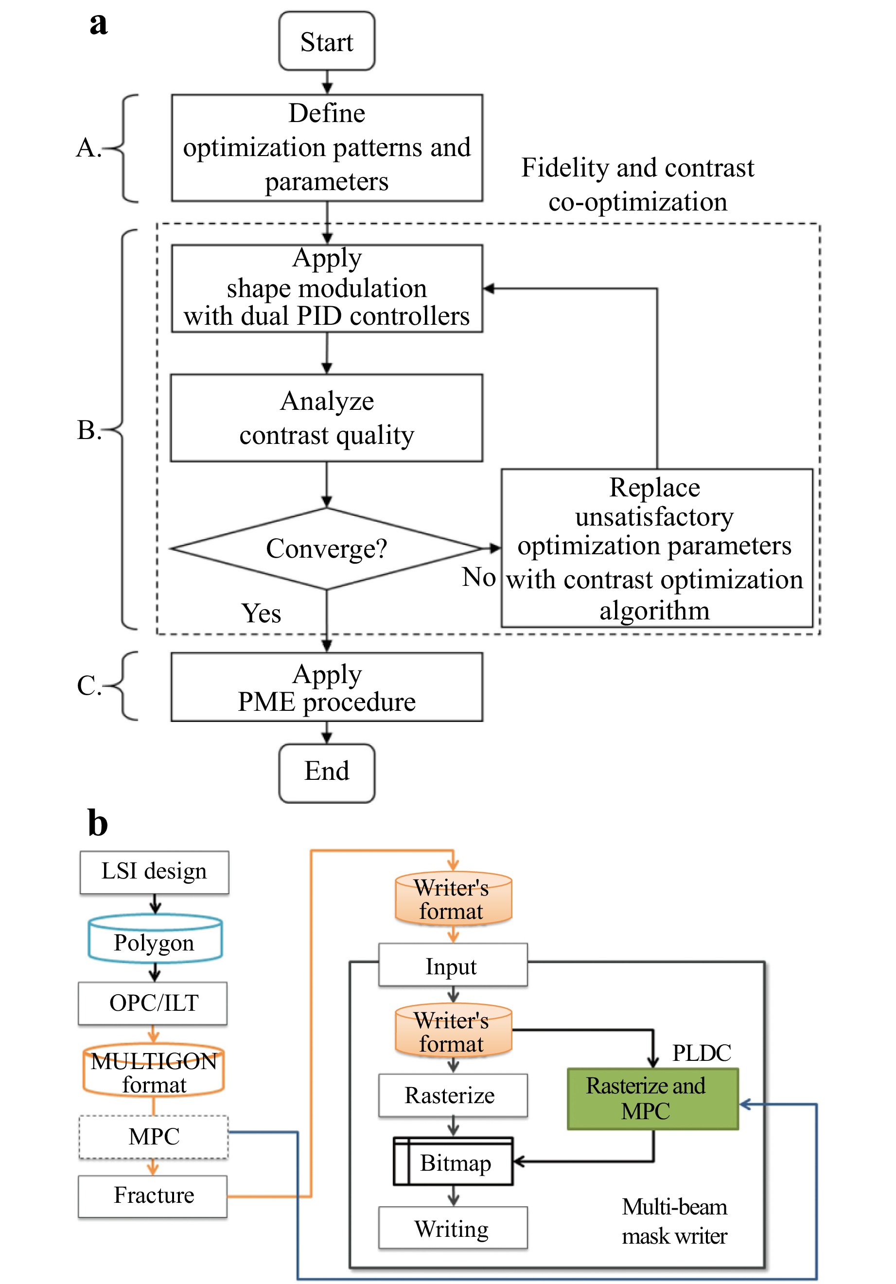
Significant progress has also been made in CLMPC workflows and paradigms. Innovations include model-based MRC pre-processing to filter non-manufacturable features81, curvature-based pre-biasing to accelerate convergence88, and integrated pipelines that combine CLMPC with Mask Data Preparation (MDP) to reduce total processing time by over 20%89. A more disruptive paradigm is pixel-level dose correction (PLDC), which embeds the MPC function directly inside the multi-beam mask writer (MBMW) (Fig. 6b). By adjusting pixel doses in real-time, PLDC eliminates the offline MPC step, dramatically shortening mask turnaround time (TAT) and achieving superior correction accuracy86. Table 3 summarizes these key research advancements in CLMPC.
Research Topic Core Content References CLMPC efficiency optimization Introduced curvature-adaptive segmentation, densifying points in high-curvature regions to optimize data and reduce runtime. 82 Fidelity improvement in high-curvature regions Proposed a shape-modulated MPC method to improve pattern fidelity in high-curvature regions. 83 Native curve MPC algorithm Developed a Bézier curve MPC flow to avoid the precision loss from piecewise linear conversion. 84 Co-optimization of fidelity and contrast Proposed a dual-layer geometric modulation method to co-optimize pattern fidelity and image contrast. 85 MPC pre-processing Proposed a model-based MPC pre-processing flow to clean up non-manufacturable fine patterns. 87 MPC convergence acceleration Proposed a curvature-based pre-biasing model to adjust patterns before the main process to accelerate convergence. 88 MPC flow innovation Proposed an integrated pipeline of CLMPC and MDP to shorten the total processing time. 89 MPC paradigm innovation Proposed a new paradigm of pixel-level dose correction, achieving online synergy between
MPC and MBMW.86 Table 3. Summary of Research Progress in Curvilinear Mask Process Correction
-
Research into CLMRC began with establishing a new theoretical framework. Pearman et al.90 posited that fundamental process blur physically defines a minimum manufacturable circle. As depicted in Fig. 7a, this concept translates complex CLMRC into intuitive rolling circle checks. This method visually evaluates manufacturability by determining if the reference circle can freely traverse all internal and external pattern contours. This philosophy not only simplifies the rules but also underscores the importance of integrating MRC constraints into the ILT optimization phase to ensure manufacturability from the outset.
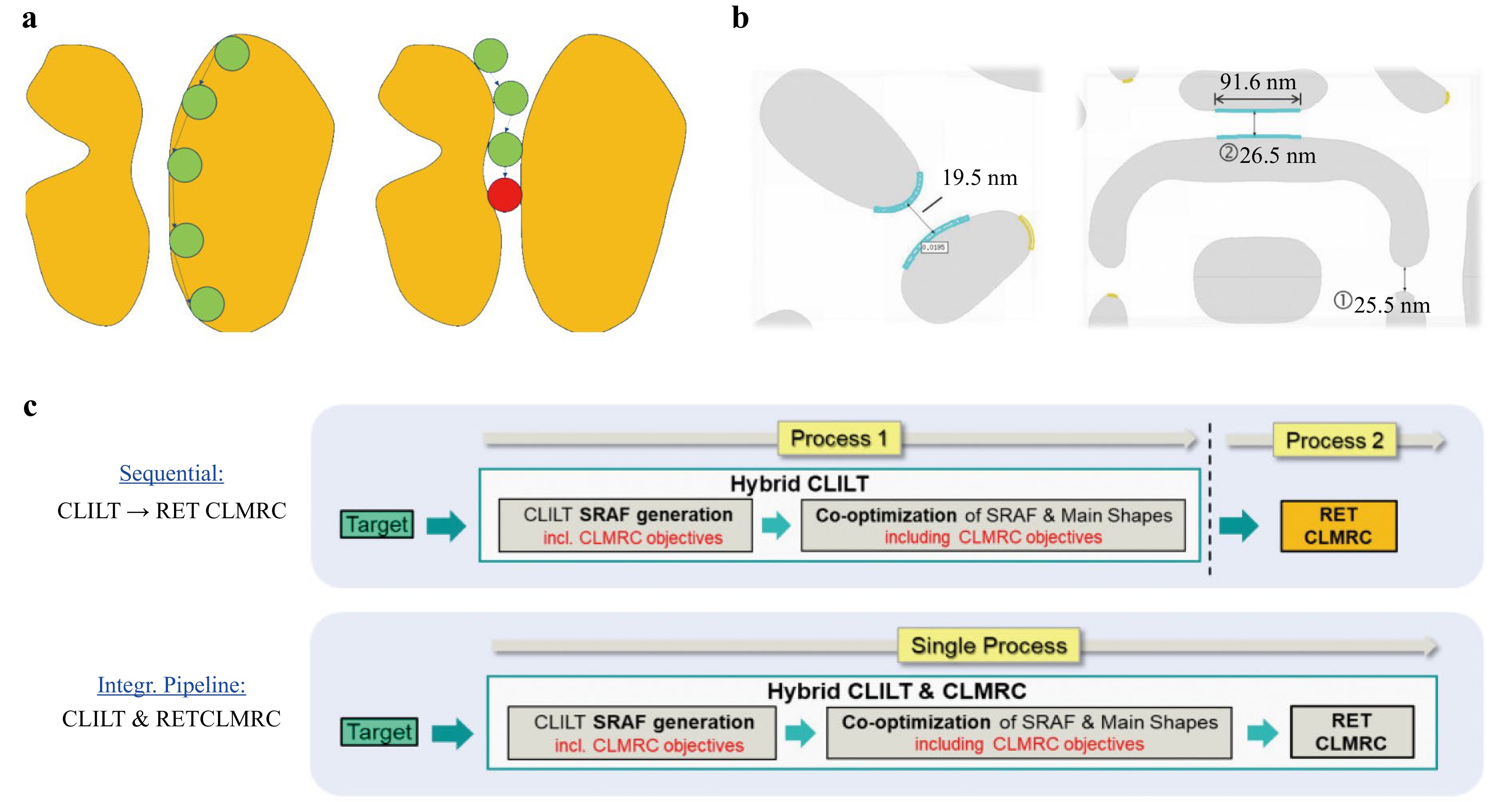
Fig. 7 CLMRC methods. a Rolling circle check schematic90. As long as the minimum circle can slide entirely within and around the features, it meets the width and space checks. Areas where the circle cannot traverse, such as the red region, indicate rule violations. b Distance check with run-length constraints40. The schematic illustrates how the spacing between two curved edges is measured. A violation is flagged only when the spacing remains too narrow over a defined continuous run-length. c Comparison of sequential versus integrated pipeline verification flows91. The top flowchart depicts a conventional process with intermediate data writing. The bottom flowchart shows the integrated approach where ILT and MRC share a single execution process without intermediate data transfers.
Subsequently, Bork et al.40 proposed a comprehensive CLMRC rule set. As illustrated in Fig. 7b, this approach introduces a run-length constraint for distance evaluation. By requiring features to violate the minimum distance over a specified length, this geometric constraint strictly distinguishes acceptable point-to-point proximity from high-risk edge-to-edge proximity. It effectively isolates true bridging hazards without triggering false violations.
Following these foundational concepts, research focused on precise and efficient execution. Early methods that digitized curves into PWL polygons were shown by Kim et al.92 to be inaccurate for sensitive parameters like curvature, where results fluctuate with segmentation resolution. To resolve this, native MRC algorithms operating directly on the mathematical definition of Bézier curves were developed, improving both accuracy and speed. In 2024, Siemens93 introduced a Bézier-based check algorithm suite with advanced functions, which runs faster and produces smaller files than PWL methods, resolving the trade-off between accuracy and efficiency. In the same year, to address full-chip verification challenges, Siemens91 proposed an integrated verification pipeline. Fig. 7c compares this integrated flow against the traditional sequential workflow. The integrated pipeline merges CLMRC and curvilinear ILT within a single rule execution. This architectural consolidation eliminates intermediate data input/output (I/O) overhead. Consequently, it significantly reduces the total TAT for full-chip verification. Table 4 illustrates the evolution of CLMRC technology from theoretical formulation to workflow innovation.
Research Topic Core Content References MRC theory based on physical limitations Proposed a rolling circle inspection theory based on the Minimum Manufacturable Circle. 90 MRC rule set with length constraints Established a comprehensive CLMRC rule set that includes run-length constraints. 40 MRC algorithm for native curve data Developed a native curvature check algorithm to avoid precision loss from digitization. 92 Advanced native curve checking functions Established a native curve algorithm set that includes advanced checks for depth width ratio and sharp corners. 93 Integrated MRC verification flow Proposed an integrated verification pipeline to shorten full-chip verification time. 91 Table 4. Summary of Research Progress in Curvilinear Mask Rule Check
-
To transition curvilinear masks from theory to high-volume manufacturing, the industry has pursued two primary technical paths. The first is the development of novel MBMW systems41, 94-96, whose pixelated writing principle is inherently suited for curvilinear patterns. The second involves applying innovative mask-wafer co-optimization (MWCO) technology97, 98 to reduce write times on conventional variable-shaped beam (VSB) writers.
-
Before the advent of MBMW, complex curvilinear masks generated by ILT were considered unmanufacturable, as conventional VSB systems could not fabricate them in a reasonable time99. This barrier was overcome starting in 2012, when IMS developed a proof-of-concept (POC) tool that verified performance for the 7 nm node. This led to the first production-capable MBMW-101 in 2016, enabling large-scale curvilinear mask manufacturing94. Concurrently, NuFlare began developing its MBM-1000 in 2012, bringing it to market in 201741. Both companies have since iterated on their systems for advanced nodes, with IMS developing the MBMW-201 and -301 systems98 and NuFlare releasing the MBM-2000 and -3000 series95, 96.
The MBMW working principle is illustrated in Fig. 8a100. A wide electron beam is shaped and directed onto an aperture plate system (APS), which divides it into hundreds of thousands of individual micro-beams. A blanking chip then electrostatically deflects unwanted beamlets, which are subsequently blocked, while undeflected beamlets pass through to be demagnified and focused onto the mask substrate. As the stage moves continuously, the array of beamlets raster-scans the design, exposing the pattern in a pixelated fashion.
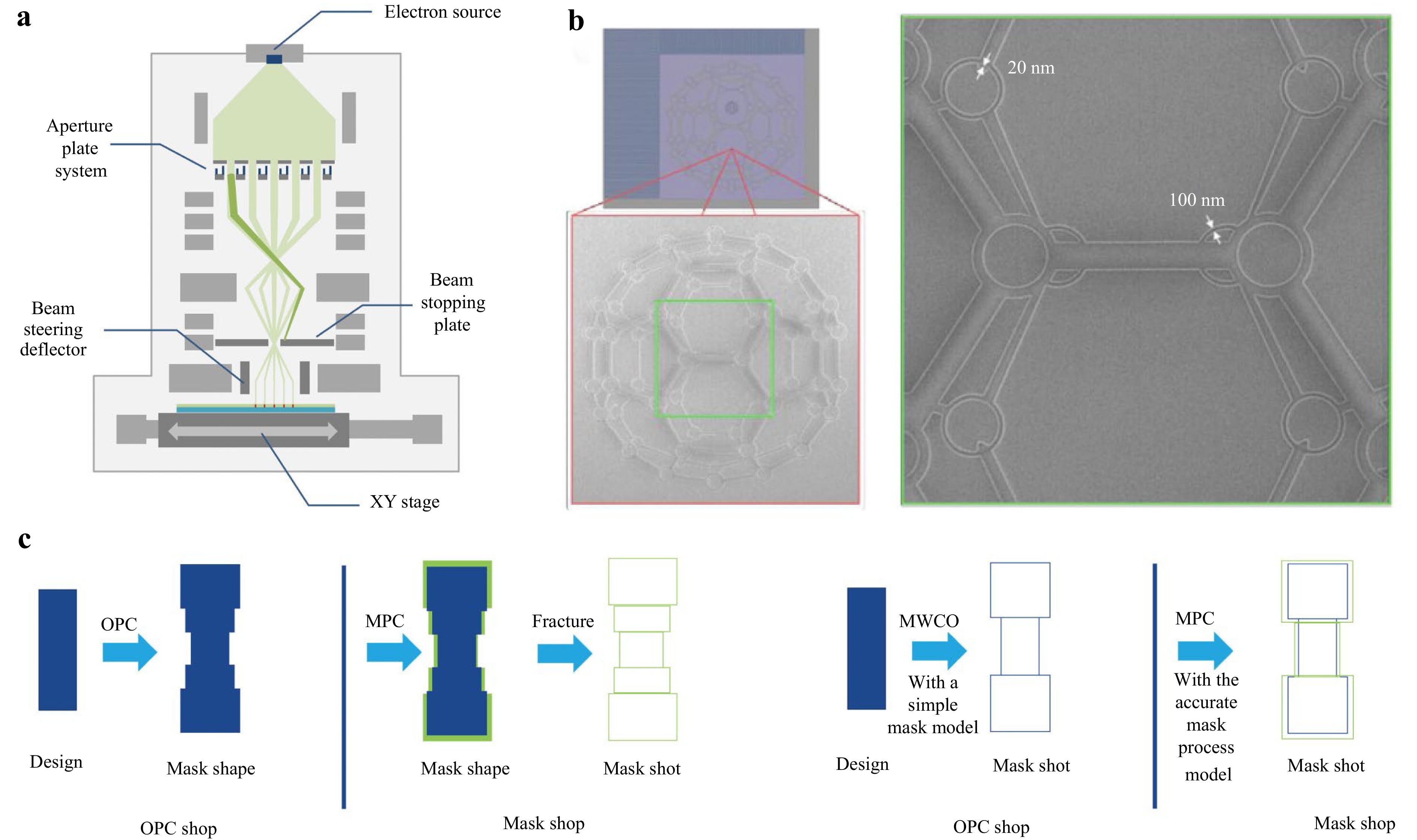
This massively parallel, pixelated architecture offers unique advantages for curvilinear mask fabrication. First, its write time is independent of pattern complexity, which overcomes the shot-count explosion and excessive write times inherent to VSB technology. Second, MBMW provides exceptional pattern fidelity, with its pixelated method capable of reproducing fine, arbitrary-angle curves with high resolution. For instance, a resolution as low as 20 nm was achieved on a "Bucky-Ball" test pattern (Fig. 8b)94. This combination of advantages establishes MBMW as a key enabling technology for curvilinear mask manufacturing in the EUV lithography era.
-
To address excessive write times on VSB writers, D2S proposed the software-driven MWCO technology. The core principle of MWCO is to integrate VSB physical constraints into the ILT optimization loop, shifting the optimization target from mask pattern fidelity to final on-wafer image fidelity97. This fundamentally alters the design-to-manufacturing handoff from mask shapes to a list of exposure shots (Fig. 8c)98.
The workflow begins with a rule-compliant curvilinear ILT pattern, which is approximated using overlapping shots to reduce the shot count. An iterative optimization loop, driven by a dual mask-wafer simulation, then adjusts shot positions and sizes to minimize the final wafer error. Experimental data demonstrates that MWCO reduces shot density to acceptable levels; for a complex contact hole array, it successfully kept the shot density below the 36 shots/µm2 threshold, thereby enabling a significant reduction in VSB write time98.
-
Precise inspection of photomask quality is critical to ensure high-fidelity pattern transfer to the wafer. Traditional 1D CD metrology, while effective for Manhattan patterns, cannot accurately assess inherently 2D curvilinear patterns101. This challenge has driven a shift toward a 2D contour-based metrology paradigm, which relies on extracting actual mask contours from scanning electron microscope (SEM) images for comparison against design targets.
Making this paradigm viable for high-volume manufacturing (HVM) has driven several key research efforts. Pang et al.102, 103 proposed an equivalent CD standard for curvilinear masks based on statistical Edge Placement Error (sEPE). As visualized in Fig. 9a, high-density measurement gauges project outward from the target contour to extract local EPE values from the printed SEM contour. This dense sampling strategy mathematically captures the 2D variation of the entire shape. This standard defines the equivalent CD as twice the sEPE, equivalent Line Edge Roughness (LER) as Local EPE Variation (LEPEV), and equivalent CDU as the uniformity of 2x sEPE. To establish a feedback loop between design and manufacturing, Delorme et al.104 proposed an innovative metrology flow. Fig. 9b illustrates this physical process. The system extracts the actual printed contour from a SEM micrograph and aligns it directly with the original design target. This geometric overlay enables continuous EPE calculations along the curve. This method correlates design parameters like local curvature with measured mask errors, providing a physical basis for defining new MRC. For efficient process qualification, a team at IMEC105 designed dedicated test patterns and a method based on measuring EPE at points of maximum curvature. However, the computational overhead of contour-based methods remains a barrier to HVM. To address this, TSMC developed a hybrid in-house metrology system101. Fig. 9c details this computational workflow. The algorithm categorizes pattern segments based on their local curvature. It applies traditional 1D CD measurements to straightforward low-curvature regions. Conversely, it reserves intensive full-contour EPE analysis solely for complex, high-curvature geometries. This parallel processing architecture ensures a viable path for HVM quality control.
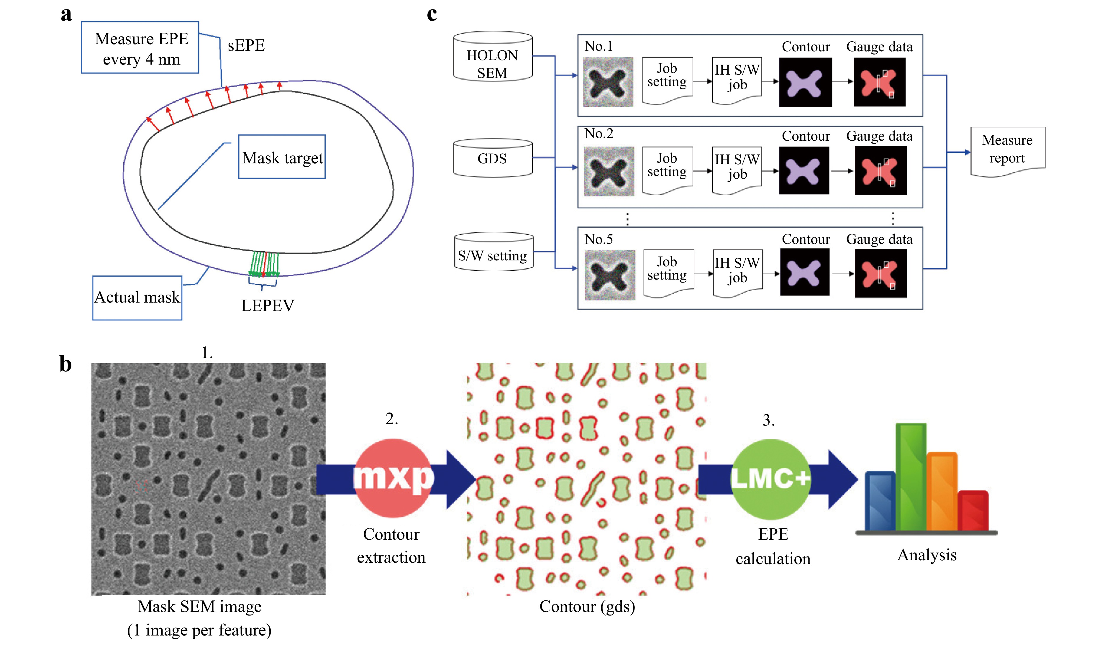
Fig. 9 Wafer metrology for curvilinear masks. a Statistical EPE measurement schematic102. Multiple perpendicular gauge lines extend from the target boundary to intersect the printed contour. b Contour-based metrology flow integrating SEM images and design targets104. A continuous contour is extracted from a raw SEM image and geometrically overlaid onto the reference design polygon. c Calculation workflow for a hybrid in-house metrology system101. An algorithmic decision path routes simple edges to 1D evaluation and complex curves to 2D contour analysis.
Beyond the computational challenges of current HVM, the transition to High-NA EUV lithography imposes strictly compressed EPE budgets and introduces new physical effects due to anamorphic optics. Recent studies from IMEC highlight that High-NA masks exhibit significant pattern asymmetry, which necessitates specialized characterization of feature dimensions unique to the 0.55 NA era106. To address the massive data requirements for global EPE qualification, large field-of-view (LFOV) contour-based metrology has been deployed to efficiently extract high-density 2D contours across expansive regions107. Complementing these efforts, researchers at Hitachi High-Tech demonstrated that integrating LFOV with die-to-database (D2DB) inspection significantly enhances stochastic defect detection, further validating the necessity of 2D inline monitoring108. Concurrently, closing the EPE control loop requires rigorous mask CD-SEM metrology matching to accurately correlate simulated curvilinear contours with final High-NA wafer prints109, 110. Together, these integrated solutions from global lithography hubs form the essential infrastructure to ensure that curvilinear mask technology can reliably mitigate the severe EPE constraints introduced by High-NA optics. Table 5 summarizes these key advancements.
Research Topic Core Content References New standard for equivalent CD measurement Proposed new measurement standards for equivalent CD, LER, and CDU based on statistical EPE. 107, 108 Design-Error correlation analysis Quantified the correlation between design parameters like local curvature and mask EPE. 104 Development of dedicated test structures Designed special test patterns to verify the impact of factors like curvature on EPE and to
calibrate measurement sensitivity.105 Full-chip metrology efficiency optimization Developed a hybrid measurement mode and parallel computing to shorten full-chip TAT. 101 High-NA holistic metrology frameworks Integrated LFOV contour metrology, D2DB stochastic defect inspection, and mask CD-SEM
matching to mitigate High-NA EPE.106-110 Table 5. Summary of Research Progress in Curvilinear Mask Wafer Metrology Technology
-
The application of curvilinear masks depends heavily on technology nodes and pattern types. For mature nodes of 14nm and above, conventional masks provide a sufficient process window with low computational cost. However, advanced nodes below 7 nm widely use EUV and High-NA EUV lithography. These nodes suffer from severe stochastic effects and physical optical limits. Therefore, curvilinear masks become necessary to maximize the process window. At the pattern level, 2D patterns like contacts naturally form circular contours on the wafer. Curvilinear patterns perfectly match these target contours. This matching significantly improves the normalized image log-slope (NILS). Other critical 2D patterns include line ends and routing corners. For line ends, curvilinear patterns prevent foreshortening and pinching. Furthermore, by smoothing sharp 90-degree bends in metal routing, they mitigate severe optical proximity effects. In addition, curvilinear SRAFs wrap around main features to provide better constructive interference. On the other hand, conventional OPC is sufficient for 1D periodic line-space patterns. Applying ILT to these simple structures causes massive data volumes and long computational runtimes. The lithographic gain does not justify this high cost.
Curvilinear masks also bring specific lithographic benefits to advanced logic and memory circuits. In logic circuits, continuous standard cell scaling requires highly dense and irregular 2D patterns. Specifically, middle-of-line local interconnects and cut layers in multi-patterning heavily rely on curvilinear masks. Printing these complex layers with curvilinear masks ensures high pattern fidelity. In advanced memory manufacturing, such as DRAM, curvilinear masks are critical for printing high-density core array structures. They are widely applied to print storage node contacts and bitline contacts arranged in dense hexagonal grids. Using curvilinear masks for these DRAM contact layers greatly increases the DOF and improves the local CDU. Both of these improvements are highly important for increasing manufacturing yield.
-
While significant advancements have been achieved across the curvilinear mask workflow, transitioning these technologies to HVM still faces critical challenges. A primary bottleneck lies in the computational complexity and runtime of full-chip ILT. Applying rigorous optical and resist models across an entire reticle demands massive computational resources. For complex routing layers at advanced nodes, the convergence of optimization algorithms requires extensive iterations. This high computational cost forces foundries to make difficult trade-offs between optimization accuracy and TAT. Furthermore, while AI accelerates this process, the limited physical interpretability of conventional deep learning models presents a reliability concern for HVM.
Compounding this complexity are the severe data volume and handling issues introduced by curvilinear mask representations. The traditional SEMI P39 OASIS format approximates curves using PWL polygons. As feature sizes shrink, maintaining acceptable pattern fidelity requires an exponential increase in polygon vertices. For sub-5nm nodes, this PWL approximation generates terabyte-scale single-layer files. This data explosion places immense pressure on data storage, transmission networks, and the overall MDP flow111. Initial PWL-based solutions, such as vertex reduction112 and CBF113, proved insufficient and introduced artifacts114. Moreover, digitizing curves into PWL polygons introduces inaccuracies for sensitive parameters like curvature during MRC. Meanwhile, traditional MPC algorithms disrupt inherent smoothness by creating artificial sharp vertices.
In the physical manufacturing domain, curvilinear masks present distinct limitations across mask writing, inspection, and metrology. During the mask writing process, conventional VSB writers suffer from a severe shot count explosion when exposing complex curves. Although MBMW effectively eliminates this write-time penalty, it introduces a new bottleneck by requiring the real-time rasterization of massive curvilinear vector data into pixelated formats. This intensive rasterization process severely overwhelms data processing systems. Subsequent mask inspection presents major difficulties because current tools struggle to reliably differentiate between intended curvilinear edge fluctuations and actual mask defects. This ambiguity severely complicates defect control, particularly for highly intricate SRAFs. Furthermore, wafer metrology lacks efficient standards for evaluating curves, as traditional 1D CD measurements cannot accurately assess inherently 2D curvilinear patterns. While contour-based metrology provides a valid alternative, extracting contours from SEM images and calculating high-density EPE require massive computational overhead, which remains a significant barrier to HVM.
At the design level, integrating curvilinear layouts into existing EDA workflows presents substantial hurdles. The current semiconductor ecosystem is fundamentally built upon Manhattan geometry. Many existing EDA tools lack native curve-handling algorithms and must resample curvilinear data back into polygons, which negates compression benefits115. Furthermore, the traditional file-based, sequential EDA workflow creates a severe TAT bottleneck due to the frequent I/O of massive files. Beyond data processing, significant physical design challenges remain. These include extending curvilinear routing beyond standard cells, enabling curvilinear routing-aware transistor placement, and optimizing wire sizing for timing closure116. To fully realize the potential of curvilinear designs, the industry requires new layout representations, advanced congestion and timing models, and algorithms capable of natively and effectively processing curved geometries.
-
Efficient data representation is a prerequisite for the industrialization of curvilinear masks. To overcome the precision loss and data redundancy of PWL approximations, the industry developed the SEMI P49 MULTIGON standard. This standard natively supports parametric curves like Bézier and B-splines35, 117. Research indicates that Bézier curves offer greater file size reduction111. They are also more conducive to OPC/MPC algorithm development118. Meanwhile, B-splines provide higher efficiency in format conversion. They better support the complex geometric operations required for High-NA EUV119.
Alongside format upgrades, achieving lossless and rapid data transfer is imperative. To eliminate the TAT bottlenecks caused by traditional file I/O, the industry is shifting toward integrated, pipelined dataflow architectures. This approach combines steps like OPC, MPC, and fracture into a single process. By passing data directly through memory, it eliminates intermediate file I/O and significantly shortens TAT101. This shift also facilitates cross-stage co-optimization. It enables the transfer of complex data structures and creates a seamless transmission model from design correction to final mask writing.
-
Future research will focus on transitioning to a highly integrated, data-driven Design-Mask-Wafer Co-Optimization (DMWCO) framework. Unlike traditional post-tape-out corrections, DMWCO proactively integrates mask constraints and lithographic models into the upstream design phase, ensuring inherent manufacturability from the earliest stages of layout generation.
Within the design domain, applying this DMWCO integration across both digital and analog circuits is a critical exploration area. In digital logic, curvilinear designs must extend from intra-cell traces to systematic cell-to-cell placement and routing. Particularly in congested middle-end-of-line (MEOL) layers, native curvilinear tracks significantly reduce via counts and parasitic RC delays. Concurrently, applying curvilinear layouts to precision analog and mixed-signal blocks, such as differential pairs, provides mathematically continuous, gridless routing. This eliminates asymmetric corner parasitics inherent to traditional Manhattan grids, ensuring absolute electrical symmetry and exact length-matching. To enable these cross-domain applications, the EDA ecosystem requires comprehensive upgrades. Future research should focus on developing native, shape-driven curvilinear routing engines, transitioning to 2D contour-aware physical verification with minimum continuous curvature constraints, and establishing precise, curve-aware 3D parasitic extraction models.
At the mask level, future research will emphasize native curvilinear synthesis and advanced fabrication. Software algorithms for OPC and MPC must process parametric curves natively to avoid the precision loss of PWL approximations. To overcome the massive computational cost of full-chip ILT, GPU-accelerated platforms and MDL are expected to become mainstream. For hardware manufacturing, future explorations will optimize MBMW data paths to efficiently fabricate complex curvilinear SRAFs without the write-time penalties of traditional VSB systems.
Furthermore, to balance the inherent trade-off between lithographic benefits and mask manufacturing difficulty in EUV mass production, the industry must adopt a multi-faceted mitigation strategy. First, modern ILT engines must actively integrate CLMRC directly into their optimization cost functions, forcing generated SRAFs to maintain a minimum radius of curvature and eliminating physically unstable features. Second, building upon the application scenarios discussed earlier, the industry is transitioning toward a mask-friendly hybrid SRAF deployment. Rather than generating extreme free-form SRAFs universally, highly intricate SRAF shapes are strictly confined to critical hotspots. For the rest of the layout, the optimization algorithms are constrained to generate simplified, highly manufacturable SRAF topologies.
Finally, at the wafer level, establishing an adaptive, closed-loop feedback system is crucial. Wafer metrology must transition from one-dimensional measurements to fully automated 2D contour analysis. Future metrology systems will require deep learning algorithms to efficiently extract high-density EPE from massive SEM datasets. Feeding this high-fidelity contour data continuously back into upstream design and mask synthesis models will systematically optimize process windows and eliminate manufacturing defects. Fig. 10 illustrates this evolution, charting the key advancements required for logic nodes from 7 nm to 1.0 nm.
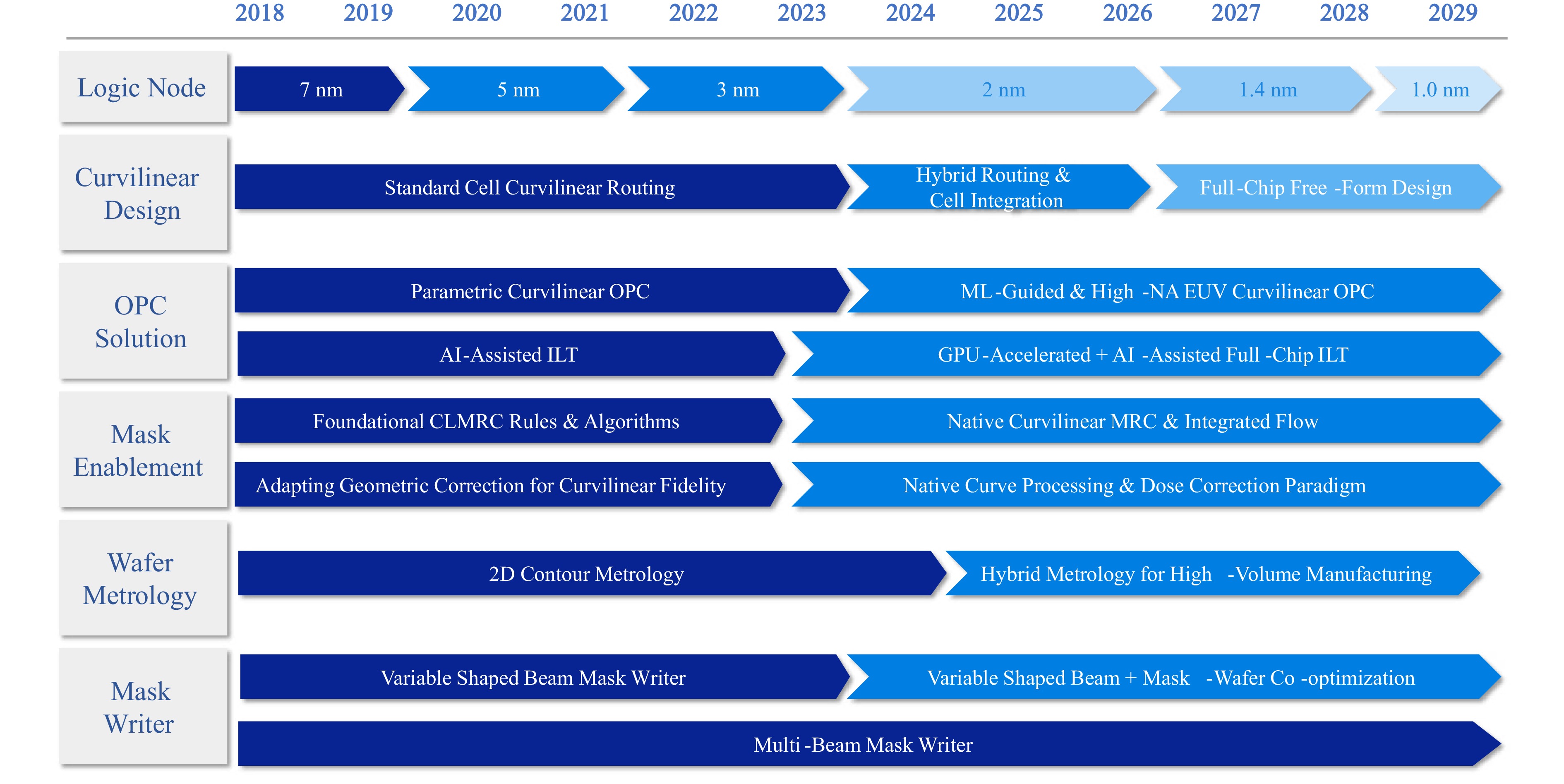
Fig. 10 Roadmap of curvilinear technology evolution.
-
Owing to its capability to overcome fundamental lithography limitations, curvilinear mask technology has emerged as a critical enabler for advanced technology nodes, particularly for complex 2D routing and dense memory arrays. This approach demonstrates exceptional performance in extending process windows, enhancing pattern fidelity, and enabling aggressive layout scaling. The barrier to high-volume manufacturing has been significantly lowered by comprehensive advancements across the entire workflow. Key breakthroughs include the maturation of curvilinear layout strategies and AI-driven correction algorithms for both optical proximity and mask process corrections. Additionally, the commercial deployment of advanced mask writing systems and contour-based metrology has secured the necessary throughput and quality control. Although full-chip adoption still faces substantial challenges regarding computational complexity, data volume management, and mask manufacturability, the industry is actively navigating these bottlenecks through hybrid deployment strategies and strict algorithmic constraints. As the ecosystem shifts toward native curve data standards, we foresee that this technology will evolve into a fully integrated DMWCO framework, driving the continued progression of integrated circuit manufacturing.
-
The work was financially supported by National Natural Science Foundation of China (Grant No.62574219), Beijing Nova Program (Grant No. 20250484884), and Beijing Natural Science Foundation (Grant No. IS26046). We acknowledge the support from IMECAS Young Talent Program (Category C) and Joint Laboratory of Microelectronics (JLFS/E‑601/24) as well.
Curvilinear mask technology for integrated circuit lithography
- Light: Advanced Manufacturing , Article number: 106 (2026)
- Received: 30 December 2025
- Revised: 18 June 2026
- Accepted: 22 June 2026 Published online: 15 September 2026
doi: https://doi.org/10.37188/lam.2026.106
Abstract: As the pivotal patterning technique in integrated circuit manufacturing, optical lithography is the principal driver of Moore’s Law. However, at advanced technology nodes, lithography confronts fundamental challenges from diffraction effects, equipment bottlenecks, and stochastic process variations, which severely narrow the process window and impede manufacturing yield. Curvilinear mask technology, an approach derived from inverse lithography technology, has emerged as a potential solution to transcend these limitations. This study provides a comprehensive overview of the technology, detailing its underlying principles and advantages in manufacturing and design, analysing its application scenarios and current challenges, and reviewing the progress and future directions of its key enabling technologies.
Research Summary
Curvilinear masks: Free-form patterns overcome manufacturing limits
As integrated circuit manufacturing shrinks to advanced nodes, traditional optical lithography faces severe physical and processing barriers. This prompts the adoption of curvilinear mask technology to maintain pattern fidelity and expand the manufacturing process window. Researchers from the Chinese Academy of Sciences provide a comprehensive review of this technology. The study details recent algorithmic and hardware advancements in optical proximity correction, mask rule checks, multi-beam mask writers, and 2D contour-based wafer metrology. The team analyze specific application scenarios alongside high-volume manufacturing challenges, particularly computational complexity and massive data volumes. Addressing these bottlenecks requires a transition toward native curve data standards and an integrated Design-Mask-Wafer Co-Optimization framework.
Rights and permissions
Open Access This article is licensed under a Creative Commons Attribution 4.0 International License, which permits use, sharing, adaptation, distribution and reproduction in any medium or format, as long as you give appropriate credit to the original author(s) and the source, provide a link to the Creative Commons license, and indicate if changes were made. The images or other third party material in this article are included in the article′s Creative Commons license, unless indicated otherwise in a credit line to the material. If material is not included in the article′s Creative Commons license and your intended use is not permitted by statutory regulation or exceeds the permitted use, you will need to obtain permission directly from the copyright holder. To view a copy of this license, visit http://creativecommons.org/licenses/by/4.0/.

 DownLoad: