






HTML
-
Multi-photon polymerization (MPP) has emerged as a powerful fabrication technique for creating three-dimensional micro- and nano-structures. In recent years, its use has grown substanially1 and it is now widely applied across a broad range of scientific and technological fields2− 6. A key advantage of MPP is its ability to fabricate arbitrarily shaped 3D structures with feature sizes down to approximately 100 nm7.
These small feature sizes are achieved by focusing an ultrashort pulsed laser into a photosensitive material8. The high peak intensity within the focal volume enables the nonlinear absorption process in which multiple photons are simultaneously absorbed by a single molecule9. The combined photon energy initiates a localized polymerization reaction that solidifies the material only at the focal point10.
Because the photoresist is transparent at the laser wavelength, linear absorption outside the focus is negligible. Polymerization therefore occurs only where the photon density exceeds the threshold required for multi-photon absorption11. This threshold and nonlinear intensity dependence confines the reaction to a sub-diffraction-limited volume, enabling the fabrication of structures with feature sizes smaller than the diffraction limit and allowing highly precise 3D microfabrication12.
In order to achieve a sufficiently high photon density to enable MPP, conventionally ultrashort pulse lasers with peak powers ranging from kW to tens of kW are utilized13 which reach peak intensities of a few TW/cm2 14. The peak intensity is a primary contributing factor in the polymerization process, directly influencing the size of the polymerized volume15. Therefore, if the peak intensity is insufficient, polymerization will not occur. Consequently, to date, ultrashort pulse lasers operating in the W regime reaching peak intensities in the tens of GW/cm2 regime have not been utilized for MPP. However, these lasers have the potential to offer significant advantages, including their compact size and cost-effectiveness. Thus, a reduction in the size and cost of MPP systems could be achieved.
This objective remains critical for MPP, as evidenced by the recent work of Messer et al.16, who achieved a compact nanoprinter using a cw diode laser and two-step absorption, which was improved subsequently by incorporating a digital micromirror device for multi-beam processing17. However, this technique requires special materials capable of two-step absorption. While the current research focuses on increasing the number of photoresists and photoinitiators for two-step absorption18, the number of suitable photoresists remains limited. This reduces the versatility of the process by neglecting a key advantage of MPP: its processing compatibility with a wide range of materials, ranging from conventional acrylate-based resins to hybrid organic–inorganic materials19 and tailored photoinitiators20. This compatibility facilitates the fabrication of micro- and nano-structures with tunable mechanical, optical, and chemical properties11. A small material variety was also observed in a previous study on a quasi-cw 405 nm diode laser, which was capable of achieving 3D microstructures by MPP only for specific materials with the capacity for nonlinear absorption at the 405 nm wavelength21.
In order to maintain the advantage of a wide range of materials, multi-photon absorption is required. One potential class of lasers for MPP could be monolithically integrated mode-locked diode lasers operating with peak powers in the W regime reaching peak intensities around several tens of GW/cm2. In comparison to state-of-the-art ultrashort pulse lasers, such as fiber lasers or titanium:sapphire lasers operating in the tens of kw regime, diode lasers offer a less complex and much more cost-effective solution. These lasers are characterized by their extremely small footprint, direct electrical pumping, and suitability for mass production. However, in addition to the significantly lower peak power and therefore lower peak intensities, the beam quality of these diode lasers is inferior to that of state-of-the-art ultrashort pulse lasers.
As a result, early demonstrations of diode laser-based MPP required multiple scans22 or external amplification23 to write a single line. These demonstrations were only a first proof of concept, as the writing velocities were below 0.1 mm/s and did not allow for the fabrication of complex objects.
Consequently, improvements to the diode laser were necessary. Initially, the central laser wavelength was modified to align with the two-photon absorption peak of conventional photoresists. This adjustment was achieved by modifying the semiconductor design of the diode laser. Secondly, the output power of the diode laser was significantly increased. This objective was accomplished by integrating a tapered waveguide on the chip24. These tapered gain sections increase the output power while keeping the beam quality high25.
This work presents the advancements in monolithically integrated mode-locked diode laser-based MPP achieved through this newly developed laser source. The processing speed was increased by three orders of magnitude compared to the last demonstrated diode laser-based MPP process, resulting in the fabrication of the first monolithically integrated mode-locked diode laser-based three-dimensional microstructures at conventional processing speeds of 100 mm/s with peak powers in the W regime and peak intensities of tens of GW/cm2. The present study analyzes and explains the reasons why high scan speed MPP becomes possible under these low peak intensity conditions. The utilized diode laser and the necessary optical setup are presented, and the fabricated 3D structures are analyzed. Furthermore, the possible minimal feature size is determined by an in-depth analysis.
-
The utilized diode laser is a monolithically integrated mode-locked GaAsP single quantum well edge-emitting diode laser consisting of a saturable absorber segment, an index-guided ridge waveguide (RW) gain segment, and a tapered (TP) gain segment as described in more detail in Ref. 26. Since the peak power of the laser source determines the peak intensity, which is a main contributor to the efficiency of the MPP process, a TP gain segment was implemented because it significantly increases the output power27. Additionally, the GaAsP material combination yielded a central wavelength of around 780 nm, which is suitable for two-photon absorption with conventional MPP photoresists and photoinitiators.
The operating parameters of the laser that result in the highest peak power were determined through an in-depth study. The pulse length of the diode laser was measured with an autocorrelator (PulseCheck 150, APE Angewandte Physik und Elektronik GmbH), the emission spectrum was measured with an optical spectrum analyzer (Optical Spectrum Analyzer AQ6370B, Yokogawa Electric Corporation), and the average output power was measured with a power meter (PowerMax PM30 and FieldMax II-T, Coherent Corp.). The autocorrelation and optical spectrum measurement data at the operating point with the highest peak power are provided in the Supplementary Information (Fig. S1).
At this operating point, the diode emits an average power of 3.45 W at a center wavelength of 777 nm with a repetition frequency of 13.2 GHz and a pulse width of 7.7 ps, resulting in a pulse peak power of 29.9 W. For the objectives used in this study, the peak intensity at the point with the highest laser peak power was calculated to 23 GW/cm2 for a 1.45 NA objective and 9.7 GW/cm2 for a 0.95 NA objective, respectively. Furthermore, the single pulse energy at this operating point was calculated to 260 pJ resulting in a laser fluence of 0.20 J/cm2 for the 1.45 NA objective and 0.09 J/cm2 for the 0.95 NA objective, respectively.
The peak power is significantly higher than that of monolithically integrated mode-locked diode lasers used in previous studies for MPP ($ P_{\rm{avg}} = 60\;\mathrm{mW}, \tau = 2\;\mathrm{ps}, f_{\rm{rep}} = 12.8\;\mathrm{GHz} $)22, which achieved peak powers of only 2.1 W. Therefore, a significant increase in processing speed is expected considering that the previous laser could only polymerize lines after multiple scans at 0.01 mm/s. However, it should be noted that this diode laser also had shorter pulses, which could improve the resolution of the MPP process28.
-
The MPP printing setup is shown in Fig. 1, including detailed microscope images of the employed laser.
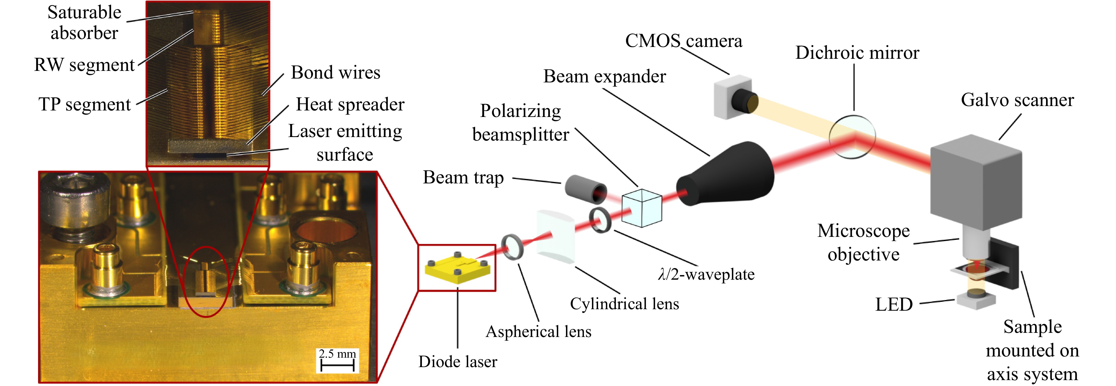
Fig. 1 Diode laser-based MPP setup with microscope optical micrograph of diode laser.
Mode-locking operation of the laser is achieved by pumping the gain segments with a controller (ITC4020, Thorlabs) and reversly biasing the saturable absorber segment with a low-noise power supply (E36312A, Keysight). During the printing procedure, the laser driver is triggered by the Galvo scanner controller. Therefore, the diode laser can easily be incorporated into a typical MPP setup.
In order to collimate the emitted laser beam, a combination of an aspherical lens and a cylindrical lens is employed. The aspherical lens is responsible for the collimation of the vertically oriented fast axis, while the subsequent cylindrical lens is responsible for the collimation of the horizontal slow axis. However, the beam profile was not perfectly circular but elliptical. The major and minor axes of the ellipse were measured to be 1.90 mm and 1.41 mm, respectively.
To facilitate a fast power adjustment, a $ \lambda / 2 $-waveplate is used in combination with a polarizing beam splitter. The implementation of a beam expander serves to enhance the focusability of the system. The subsequent dichroic mirror reflects the laser beam into the Galvo scanner (hurrySCAN II 14, SCANLAB GmbH). The MPP process is carried out in a layer-by-layer sequence. The Galvo scanner is used to deflect the laser beam inside each individual layer, while the movement between the layers and the sample positioning is achieved by three linear axes (Wafer Max Z and ANT 130-XY, Aerotech Inc.) on which the sample is mounted. A microscope objective is employed to focus the laser beam inside the photoresist. In this work, two different objectives are used for comparison (100x NA = 1.45 Plan Apo, Nikon and 40x NA = 0.95 Plan-Apochromat, Zeiss). An LED is positioned underneath the sample to allow process monitoring through the combination of the LED with the dichroic mirror and a CMOS camera.
The photoresist employed in this study is Femtobond 4B, a conventional organic-inorganic hybrid photoresist for MPP processes, which is described in further detail in the materials and methods section. This photoresist was chosen because it is representative of a standard class of photoresist for MPP.
-
In order to quantify the possible minimal feature size of the diode laser-based MPP system, two cuboid blocks connected by three lines were fabricated. The three individual lines are free-hanging and were fabricated by a single scan. Consequently, the dimensional parameters of a single voxel can be determined by measuring the height and width of the lines using SEM. To this end, two SEM images were captured: one from the top, to measure the voxel width, and one at a 45° angle, to measure the voxel height. In order to obtain the voxel height from the measured height in the image, the former was multiplied by $ \sqrt{2} $. To ensure better comparability, three sets of measurements were taken for each line: one at the center, and one at 1/4 and 3/4 of the total line length.
For comprehensive analysis, these line structures were fabricated with a 100x (NA = 1.45) objective and a 40x (NA = 0.95) objective, as well as with different scan speeds for both objectives to examine the influence on the voxel size. For both objectives, the three lines were scanned along the major axis of the raw beam profile and scanned perpendicular to it. The direction that is parallel to the major axis is now termed “x-direction”, and the direction that is perpendicular to the major axis is termed “y-direction”. The highest peak power of the diode laser was utilized for all lines. The power was subsequently measured once more behind the beam expander, resulting in 2.2 W. In Fig. 2 exemplary SEM images at a magnification of 10,000x from the top and a 45° angle of such a structure are shown. This structure was fabricated with the 100x objective and a scan speed of 0.5 mm/s. Scan speeds in the range of a few mm/s were utilized, as the maximum speed for individual lines is significantly smaller than for 3D structures due to the proximity effect29.
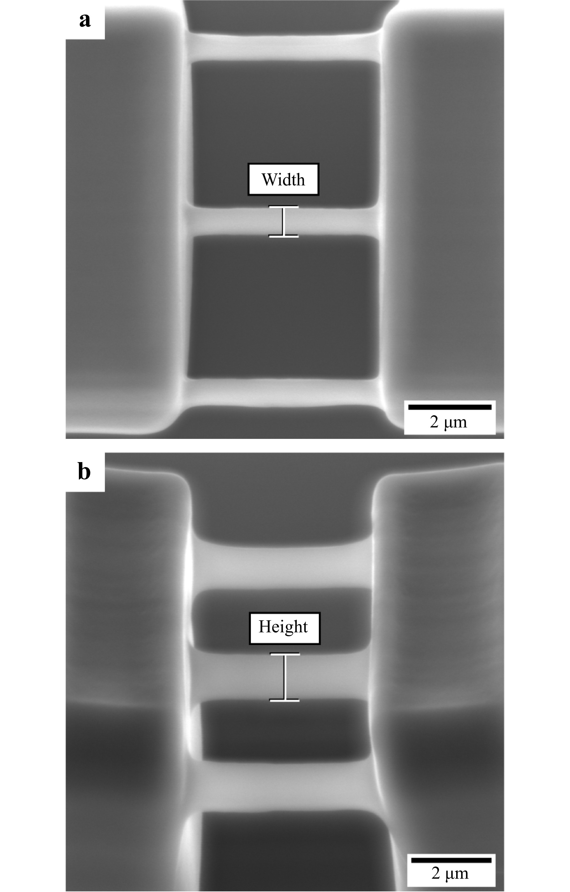
Fig. 2 SEM images of lines of overlapping voxels captured from the top a and at a 45° angle b. The width was measured directly from the images. Due to the 45° viewing angle, the height was calculated by multiplying the measured height by $\sqrt{2}$.
Therefore, the maximum scan speed at which all three lines could be fabricated with consistent stability was determined. This was achieved by increasing the scan speed for both objectives until not all lines were visible under the SEM. For the 40x objective, the maximum scan speed was 2 mm/s, and for the 100x objective, it was 5 mm/s. Furthermore, the structure was fabricated with ten distinct scan speeds, with equal intervals to the maximum scan speed in both scan directions of the scanner. To calculate average values and standard deviations for the voxel dimension, the height and width of all three lines were measured at three points each. The results are presented in Fig. 3.
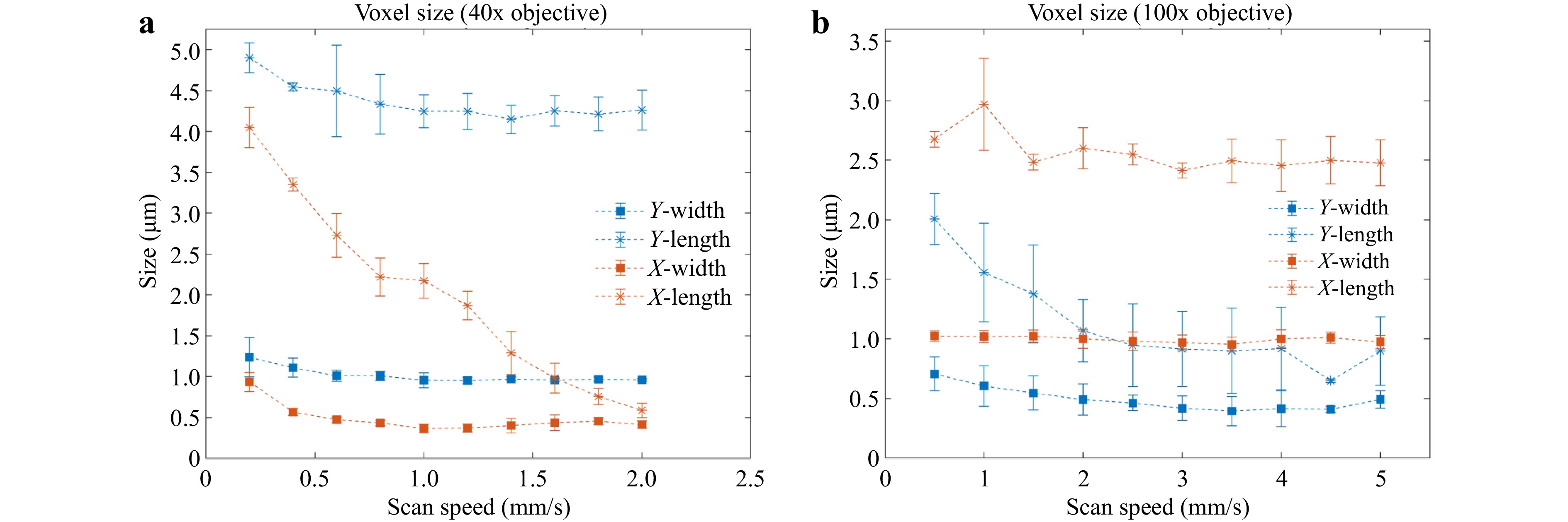
Fig. 3 Voxel dimensions as a function of scan speed for the 40× objective a and the 100× objective b. The x-direction indicates scanning along the major axis of the raw beam profile, and the y-direction scanning is perpendicular to the major axis.
In Fig. 3a, the voxel dimensions for the 40x objective are displayed, while Fig. 3b presents the voxel dimensions for the 100x objective. The star-shaped data points indicate the voxel height, while the square-shaped markers represent the voxel width. The dimensions calculated from lines fabricated in the x-direction of the scanner are represented in orange, while the dimensions calculated from lines fabricated in the y-direction are represented in blue.
A consistent observation across all experiments indicates that the voxel size of lines fabricated with the 100x objective is smaller than for the 40x objective. Additionally, the voxel length is consistently larger than the voxel width, thereby manifesting the characteristic ellipsoid shape of MPP voxels. Furthermore, a general pattern of decreasing voxel size with increasing scan speed is evident, with this trend being more pronounced for the voxel length than for the voxel width.
However, it is noteworthy that the trend of decreasing voxel size is much lower for one fabrication direction, where both the width and height remain relatively constant. It is notable that the direction of slower decreasing voxel size varies depending on the objective, as it is the y-direction for the 40x objective and the x-direction for the 100x objective. Additionally, the direction exhibiting a smaller decrease in voxel width and length also exhibits larger voxel sizes over all fabrication speeds.
Nonetheless, the previously determined maximum scan speeds for achieving stable lines did not yield the minimum achievable voxel dimensions. At higher scan speeds, the fabrication process of single lines becomes unstable, resulting in fewer than three successfully fabricated lines after processing. Given that higher scan speeds result in smaller line geometries, it is expected that the lines will become too weak to hold by themselves. This is a typical effect also observed for conventional solid-state laser sources. However, in cases where at least one line retained structural stability, significantly smaller voxel dimensions were obtained. The smallest line was produced using the 100x objective at a scan speed of 6 mm/s, where only a single line was successfully fabricated. This line exhibited a diameter ranging from 121 nm (thinnest section) to 140 nm (thickest section), and a height ranging from 151 nm to 277 nm. A top-view SEM image of this line is presented in Fig. 4.
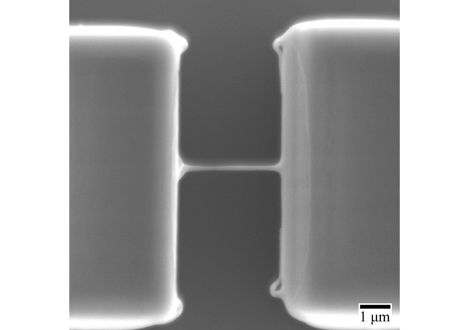
Fig. 4 Smallest line of overlapping voxels fabricated with 100x objective at 6 mm/s scan speed.
Furthermore, additional experiments were conducted to examine the influence of peak intensity on voxel size. At a constant scan speed of 1 mm/s the laser power was varied between 1 W and 1.85 W and using the 100x NA = 1.45 objective the free hanging line structures were produced as in the previous experiments. The results are illustrated in Fig. 5. It can be seen that the voxel length and width grow with a higher peak intensity. Additionally, a discrepancy in voxel size between the two scan directions is visible; the x-direction produces larger voxels, similar to Fig. 3b. Below 1.25 W of laser power, no stable lines of voxels were created when scanned in the y-direction. In addition, in some cases, a higher peak intensity results in a smaller voxel size at the next data point.
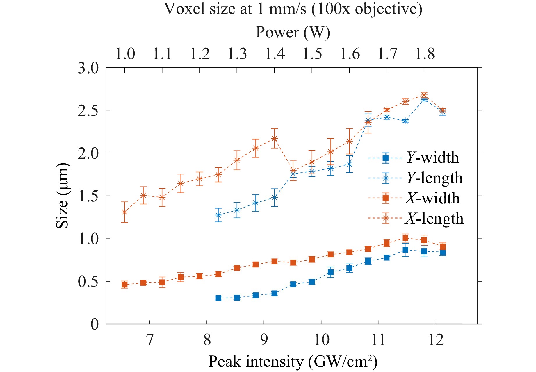
Fig. 5 Voxel dimensions as a function of laser power (top axis) and peak intensity (bottom axis) for the 100× objective. The x-direction indicates scanning along the major axis of the raw beam profile, and the y-direction scanning is perpendicular to the major axis.
These experiments revealed that the polymerization threshold is 1 W in the x-direction and 1.25 W in the y-direction at a scanning speed of 1 mm/s. Additionally, the polymerization threshold for fabricating bulk 3D structures was determined to be 1.2 W at 100 mm/s. The maximum power of the diode laser was insufficient to reach the damage threshold.
-
In order to evaluate the printing performance of the diode laser-based MPP system, further experiments including three different complex-shaped structures were performed. The first structure is a model of a fullerene molecule, the second is a scaffold structure for biomedical applications, and the last one is a mining tower, which is a landmark structure of the Ruhr University Bochum. These structures were selected to represent a range of characteristics associated to MPP processes. These include surfaces with spherical and straight geometries, as well as surfaces that are complex in shape, featuring undercuts, and exhibiting fine details. Images of the STL files used for all three structures can be found in the Supplementary Information (Fig. S2). Fabrication of all models was conducted using the 100x NA = 1.45 objective lens in a layer-by-layer manner, with the initial layer starting at the glass to photoresist interface. The complete list of all processing parameters is listed in Table 1. By rotating the $ \lambda / 2 $-waveplate, the average laser power was reduced to 1.6 W (resulting in a peak power of 13.9 W and a calculated peak intensity of 11 GW/cm2), which minimized overpolymerization and ensured optimal resolution. Its measurement was conducted directly behind the beam expander.
parameter value unit layer thickness 0.1 µm hatch distance 0.1 µm average laser power 1.6 W peak power 13.9 W calculated peak intensity 11 GW/cm2 pulse energy 120 pJ calculated laser fluence 0.09 J/cm2 Table 1. Process parameters
In Fig. 6, scanning electron microscopy (SEM) micrographs of all three structures are shown. The fabrication of these structures was successfully achieved through the use of diode laser-based MPP, as evidenced by the intricate features of the structures being sharply defined. Furthermore, the structural stability of the samples is validated even for substantial undercuts, especially demonstrated for the fullerene structure. Additionally, the structures exhibit a sufficient surface quality for both round and flat surfaces. The fine details of the mining tower are also well defined, displaying sharp contours. Moreover, the scan speed of 100 mm/s enabled the rapid fabrication of all three structures. The MPP processing for the fullerene structure required 8 minutes, the scaffold structure required 12 minutes, and the mining tower was processed in 7.5 minutes.
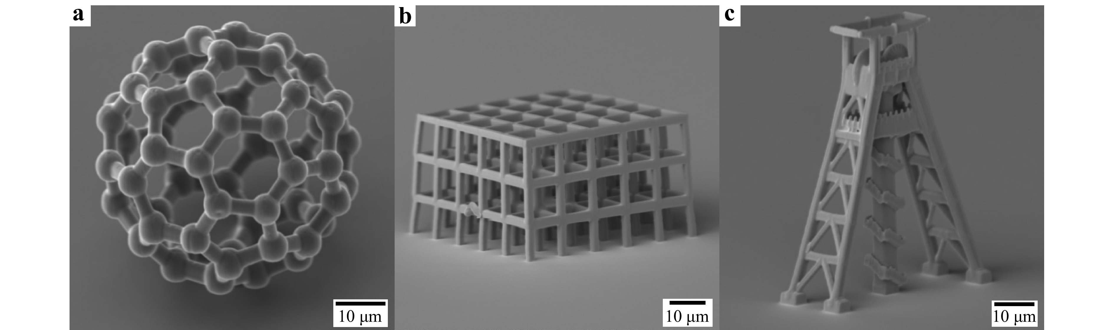
Fig. 6 SEM images of fullerene molecule model a, scaffold structure b and Bochums city landmark mining tower c fabricated by diode laser-based MPP.
As a multitude of applications of MPP necessitate the fabrication of numerous repeated or large-scale structures over an extended period, a measurement of the power stability of the diode laser was conducted over a duration of 64 hours. During this period, the power deviation remained below 0.3 %, thereby suggesting the feasibility of such fabrications with the diode laser. The complete measurement can be found in the supplementary information (Figure S3).
-
This work demonstrates the feasibility of MPP fabrication of complex structures at high scan speeds, up to 100 mm/s, using monolithically integrated mode-locked diode lasers. This is particularly remarkable given the significantly lower peak power and resulting lower peak intensity of diode lasers compared to conventionally employed laser sources. While Ti:Sa lasers and fiber lasers typically operate with peak powers in the kW range reaching peak intensities of a few TW/cm2, the mode-locked diode laser used in this work delivered a maximum peak power of approximately 30 W and reached a peak intensity of 23 GW/cm2.
An explanation for the MPP process's functionality with low peak intensities is the considerably higher repetition rate. The repetition rate of 13.2 GHz is more than two orders of magnitude higher than that of a conventional Ti:Sa or fiber laser, which typically operates around 80 MHz. According to previously determined findings, an increase in repetition rate results in a less pronounced nonlinearity of the MPP process30, 31. Therefore, the two orders of magnitude smaller peak intensity could potentially be compensated by the two orders of magnitude higher repetition rate. Furthermore, recent studies have demonstrated that the process window of MPP is broadened by employing shorter wavelength lasers9, which could be advantageous for the diode laser emitting at 777 nm, which is shorter than commonly used 800 nm lasers.
A noteworthy observation is the difference in the voxel dimensions depending on the laser scan direction, both when varying the laser power and the scanning speed. It is evident that in one direction significantly smaller voxel widths and lengths are observed, resulting in different polymerization thresholds, while accompanied by a substantially more rapid decrease in size with increasing scan speed. One potential explanation for this phenomenon could be the direction of the polarization of the laser, as its influence on the line width has been previously demonstrated in the literature32. However, this effect was observed to be considerably less pronounced in terms of the line dimension than the one observed in this study.
Another possible explanation could be ellipticity or astigmatism, which is an inevitable occurrence in the emission of tapered diode lasers. Despite the collimation comprising a combination of multiple lenses, the laser still exhibits residual astigmatism and an elliptical beam shape.
When focusing a beam with astigmatism, it is observed that there is not a single focus, but rather, the horizontal and vertical beam axes have different foci. Consequently, the beam shape in the focal region could manifest as an ellipse rather than a circle. When lines are fabricated in the direction of the major axis of the ellipse, smaller line diameters can be fabricated since the minor axis is perpendicular to the scan direction. However, when scanning in the direction of the minor axis, the larger major axis is perpendicular to the scanning direction. This results in a much larger irradiated area and a wider polymerized line. This phenomenon offers a plausible explanation for the observed variation in size, but it does not provide a satisfactory explanation for the disparity in size reduction rates between the two directions.
Moreover, it is important to note that the direction changes between the 40x objective and the 100x objective. Subsequent analysis of the focal spot shape revealed that the minor and major axes of the 100x and 40x objectives are perpendicular to each other. This phenomenon may be attributed to the complex optical configuration present within both objectives.
The disparity in size between the scan directions is negligible for the 3D structures presented here. However, for structures exhibiting significantly smaller features, such as metamaterials and photonic crystals, this discrepancy may become a limiting factor.
During the fabrication of complex structures, the maximum power of the diode laser resulted in overpolymerization and a subsequent loss of structural detail. Therefore, the actual utilized average power was reduced to 1.6 W using a $ \lambda / 2 $-waveplate and a polarizing beam splitter, corresponding to an effective peak power of approximately 13.9 W and a peak intensity of 11 GW/cm2. At this reduced power level, high processing speeds were achieved without compromising structural resolution, enabling the successful fabrication of fine, detailed features.
It is noteworthy that the maximum scan speed of stable single lines with the 100x objective was 5 mm/s, whereas the 3D structures were fabricated with 100 mm/s and demonstrated perfect stability, even with overhangs. This phenomenon can be attributed to the proximity effect, a well-documented effect that has been observed with conventional laser sources as well29.
When a single line is scanned at high speeds, the deposited energy dose per voxel can be insufficient to initiate polymerization, as the polymerization threshold is not surpassed. Nevertheless, multi-photon absorption still generates radicals. These radicals alone do not reach the critical concentration required for polymerization. However, when a subsequent scan line is written shortly afterwards and in close spatial proximity, such as with the hatch distance of 100 nm used in this work, the irradiated volumes partially overlap and additional radicals are generated. In the overlapping region, radicals from successive exposures accumulate, leading to a sufficiently high radical density to initiate polymerization.
This cumulative mechanism is possible due to the relatively long lifetimes of radicals compared to the time between neighboring scan events. Radicals generated during the first exposure can therefore persist and contribute to the radical population generated by subsequent exposures33. Additionally, diffusion of radicals can transport reactive species into adjacent regions, further increasing the effective radical concentration between neighboring scan paths34.
Consequently, when all lines of a structure are sufficiently close to one another, the accumulated radical population in overlapping exposure volumes enables stable polymerization throughout the structure. Furthermore, the significantly higher repetition rate of the diode laser in the GHz regime, compared to the MHz regimes of common fiber and Ti:Sa lasers, results in much larger voxel overlap in each line, thereby increasing the cumulative effect. This explains why complex three-dimensional structures can be fabricated at significantly higher scan speeds than isolated single lines.
The minimal achieved linewidth of 120 nm is a remarkable result, comparable with other state-of-the-art laser systems when fabricating conventional photoresists. However, it should be noted that this represents an exceptional case, as the fabrication process with this processing speed does not ensure stability for all fabricated lines. When employing lower scan speeds, reliable fabrication of all individual lines could be achieved, although at significantly larger dimensions.
In summary, the experimental findings confirm that MPP systems employing a monolithically integrated mode-locked diode laser can attain scan speeds that are competitive with those of state-of-the-art fiber lasers and Ti:Sa lasers when fabricating complex 3D microstructures. Furthermore, a fine feature size of a minimal line width of 120 nm was achieved. However, the single-line experiments exhibited a substantial direction dependence, which can be attributed to the inherent astigmatism of the tapered diode laser. This observation suggests the possibility of achieving future enhancements through the use of an optimized optical system.
This performance of the compact and cost-effective monolithically integrated mode-locked diode laser has the potential to facilitate the more widespread adoption of MPP in research and industry. Specifically, it lowers the entry barrier for MPP due to the possibility of more compact and much less expensive MPP systems. Moreover, due to the compact laser size, parallel multi-beam processing using several diode lasers could become feasible in the future to increase the throughput of MPP. The present MPP process limitation of low processing speeds would be resolved by this solution, which could therefore enable many new applications of MPP as larger areas of MPP structures could be fabricated. Furthermore, the popular approach of grayscale MPP35 for significantly improving surface quality36 can be considered in the future.
As a potential outlook, a prototype of a monolithically integrated diode laser-based MPP system is shown in Fig. 7. The dimensions of the system are 430 mm × 390 mm, with a height of 320 mm and a total weight of around 20 kg. The system is equipped with an openable process chamber, featuring an XYZ-axis system with a travel range of 50 mm in each direction. The complete laser beam control, collimation, and beam guiding to the Galvo Scanner (as shown in Fig. 1) is enclosed on the left side of the system. The electrical components and controllers are situated in the back and left side of the system, respectively.
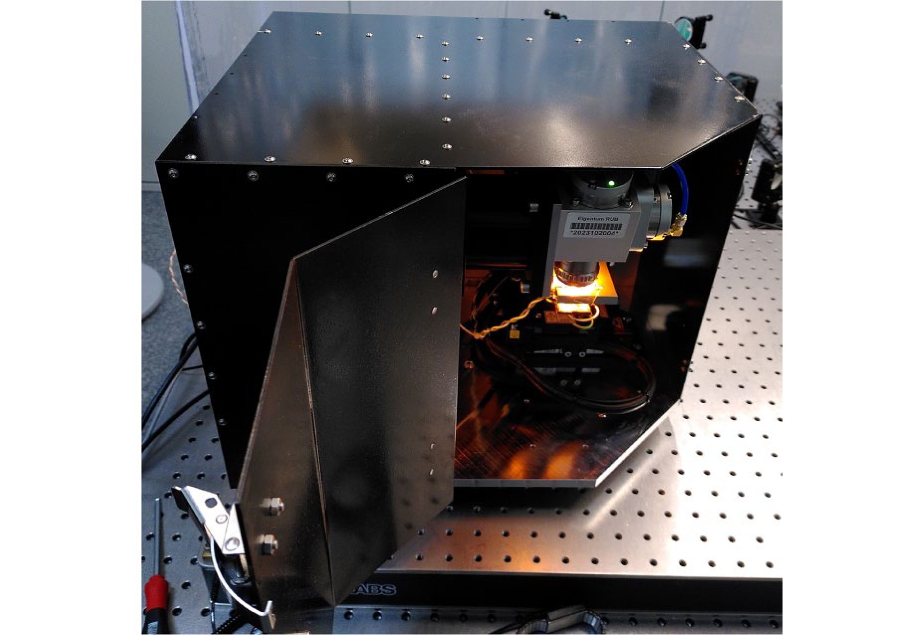
Fig. 7 Prototype diode laser based MPP setup.
-
All experiments were conducted using the Femtobond 4B photoresist (Laser Zentrum Hannover e.V., Hannover, Germany), an inorganic-organic hybrid polymer. This photoresist consists of 70% methacryloxypropyl-methylsiloxane, 15% zirconium propoxide, a photoinitiator, and solvents. This photoresist shows significant similarity to the well-known and frequently utilized photoresist SZ208037 in MPP processes. Consequently, it is a common organic-inorganic hybrid photopolymer, and it is reasonable to assume that the diode laser can be used for this class of photoresists. Nevertheless, given the existence of a multitude of photoresists belonging to different classes, further studies are necessary to examine each class individually.
The photosensitive material was pipetted onto a glass coverslip (epredia) and subsequently baked at 80°C for 30 min to remove solvents. After processing, the samples were developed by immersion in a 1:1 mixture of 2-propanol (VWR Chemicals) and 4-methyl-2-pentanone (Sigma-Aldrich).
The SEM images of the 3D structures were captured with the SEM (EVO MA10 3086, Zeiss) due to its ability of imaging at high tilting angles, and the voxel size images were imaged with the SEM (Quanta 650 FEG, FEI) due to the higher SEM resolution. Quantification of the voxel sizes was conducted using the software ImageJ.
-
The authors sincerely appreciate the financial support provided by the German Federal Ministry of Education and Research (BMBF) (FKZ: 03VP09211, MINI2PP) and the German Federal Ministry for Economic Affairs and Energy (BMWE) (FKZ: 03EFNW0386) for this project. They also extend their gratitude to Saeid Shakerinezhad for his invaluable assistance in conducting MPP-fabrication experiments.

 DownLoad: