


HTML
-
For decades, Moore's Law has guided the exponential growth of the computing capacity and manufacturing volume of silicon (Si) microelectronics, and the generated data were transported globally via long-haul fibre-optic networks. The complex long-haul network constituted the interconnect backbone to bring us into the Information Era Web 1.0. This closely interlocked tie between microelectronics and photonics becomes more crucial as optical interconnects sustain exponential traffic growth, resulting in the amount of aggregated data currently doubling itself nearly every two years1. As we enjoy Web 2.0, the rapidly increasing market demand for speed, energy efficiency, and ownership cost for both microelectronics and photonics cements the urgency for the world to enter Web 3.0, and soon Web x.0. In particular, the on-going worldwide COVID-19 pandemic further accelerates this global transformation. Therefore, the core technologies in the two major semiconductor market segments need to march forward quickly to meet technical and business expectations.
Five years ago, a Si chip containing ten billion transistors2 made the debut from a top complementary metal-oxide semiconductor (CMOS) foundry with a standard 300 mm wafer production line. Since then, the most sophisticated III-V compound semiconductor PICs surpassed one thousand components per chip3, 4, with most of them being produced in 75 mm III-V wafer production lines. Many optical transceiver products still rely on slow and labour-intensive packaging of discrete components. In contrast to microelectronics, the fact that different optical functionalities are inherently dependent on a variety of materials is a fundamental scalability roadblock for integrated photonics. Therefore, integrated photonics has traditionally been a low-volume and expensive technology. Fully acknowledging the fundamental material pitfalls of an indirect band gap and the absence of a linear electro-optic (Pockels) effect in Si prompted academia, industry, and governments to seriously start investigating and investing in the concept of ‘photonize Si’ at the onset of the new millennium. These efforts aim to create a ‘shortcut’ for photonics to eliminate this multi-generation deficiency in integration technology with help from the mature CMOS infrastructure. The global effort has paid off quickly as the plasma dispersion effect5, 6 is used as an alternative to build Si modulators7 that are capable of performing 160 Gb/s PAM4 modulation today8. Although CMOS-compatible germanium (Ge) is a natural material for the efficient detection of near-infrared optical signals9, 10, the final necessary component is still a practical Si-based laser11, 12.
Compared with the alignment of a diode laser output to a Si photonic chip in the final stage of packaging, the invention of heterogeneous III-V-on-Si lasers 15 years ago represents a major technological leap to produce a practical laser on Si13-15. In this regard, III-V thin films transferred by way of wafer bonding are similar to perfectly epitaxial grown optical gain materials on large-scale Si wafers. This essentially moves the lasing functionality enablement from the last manual chip-level production stage to an early automatic wafer-level manufacturing stage. This is a fundamental improvement in terms of fabrication precision, integration density, production volume, and efficiency. The new platform also enables multiple key technical merits favourable to laser design, operation, and active-passive integration16, 17. Since then, it has quickly emerged as the most promising on-chip source integration solution for Si photonics.
Ten years ago, along with other colleagues, we had the privilege to review a variety of light sources on Si and early stage heterogeneous III-V-on-Si photonic integration18-20. A decade of non-stop innovations, engineering perfection, and commercial development has certainly expanded heterogeneous Si photonics to a much larger multidisciplinary field for numerous applications beyond optical transceivers. Today, we appreciate this opportunity to review more recent breakthroughs and trends in this field. We first define the subject of interest in heterogeneous III-V-on-Si photonics integration and describe general wafer-bonding processes. Then, we review the state-of-the-art industrial development and commercial success built upon the first-generation demonstration, which echoes the business outlook we presented in several review articles18-20 over a decade ago. We focus on recent device- and platform-level innovations, aiming to embody the unique DNA in heterogeneous integration. This includes a) vast optionality and flexibility in material selection to drastically extend the spectrum of interest, and b) novel designs to amplify the material merits of III-V- and Si-based materials while minimizing their intrinsic pitfalls simultaneously to result in a perfect complement that extends beyond the simple combination of both. Instead of taking the conventional approach to summarise a collection of most recently published papers in this broad field, we attempt here to focus on the best but selective representative progress in academia and industry. We invite readers to review this exciting technological advance using both historical and prospective vision to appreciate the fundamental essence this innovative concept held over a decade ago and is foreseen to hold many decades ahead.
-
The words hybrid and heterogeneous have been frequently used in the literature of both microelectronics and photonics, either as interchangeable terms or by referring to different integration schemes. In this paper, we define a convention to denote heterogeneous Si photonic integration as the transfer of a non-Si, unprocessed thin-film material onto a Si substrate using a wafer-bonding technique, followed by conventional planar lightwave component or integrated circuit fabrication to realise target optical functionality. On the other hand, however, hybrid photonic integration refers to a more ‘old fashioned’ assembling scheme in which one or more completely or partially finished photonic chips, e.g. an III-V diode laser chip, is optically integrated with another chip, e.g. a Si photonic chip, via in-plane butt coupling or flip-chip packaging. We emphasise the unprocessed III-V thin film prior to wafer bonding in our definition of heterogeneous integration to embody the unique benefit of full III-V device fabrication on larger Si wafers (≥200 mm). Any fabrication on smaller III-V native substrates (e.g. ≤150 mm for InP and GaAs) will inevitably introduce a higher cost and potentially tighter alignment margin onto Si wafers because of the need for two sets of fabrication tools and the necessary alignment of features defined by different lithography systems. This slightly narrower definition allows us to more specifically focus on the design and fabrication of selected examples later.
The illustration in Fig. 1 indicates that the field of Si-based heterogeneous photonic integration has evolved into a broad technology with a strong ‘rooting system’ in the past 15 years. Large, inexpensive, strong, and low-optical loss Si wafers serve as an ideal substrate to accommodate a variety of optically functional thin-film materials including materials in Group IV, III-V and many other compounds. Robust mechanical support, excellent thermal conductivity, and the lowest cost are inherent characteristics of bulk Si if it does not involve optical waveguiding. A thin film transferred onto bulk Si would either require a higher refractive index, e.g. Ge, or a waveguiding layer stack to avoid optical leakage to the Si substrate21. A layer of low-refractive index dielectric material, such as SiO2 or SiNx, could be easily oxidized or deposited on Si to form an ‘on-insulator’ structure to provide strong optical confinement perpendicular to the substrate plane. Then a rib or ridge waveguide structure would need to be defined on top of the thin film layer to realise transverse optical mode confinement. A high-index contrast (HIC) platform such as this is realised to enable compact photonic component and high integration density on Si. The most distinct common example is SoitecTM Si-on-insulator (SOI) wafers, which were commercialized by CEA-Leti with their proprietary Smart-cut process22 and molecular wafer bonding technique23. Currently, the vast majority of Si photonic components and circuits in research and commercial products are hosted on standard SOI wafers as large as 300 mm. More functionalities can be extended on special ‘on-insulator’ substrates when compound semiconductors such as III-V24, 25 or SiC26, 27 replace the top Si layer. Finally, most heterogeneous photonic integrated structures are directly based on SOI substrates to allow seamless in-plane optical transition between the heterogeneous part and pure monolithic Si photonics. The Si device layer on SOI substrates also provides design freedom in that it allows the heterogeneous waveguide modes to be easily engineered to reside mostly upward in the thin film or downward to the Si layer.
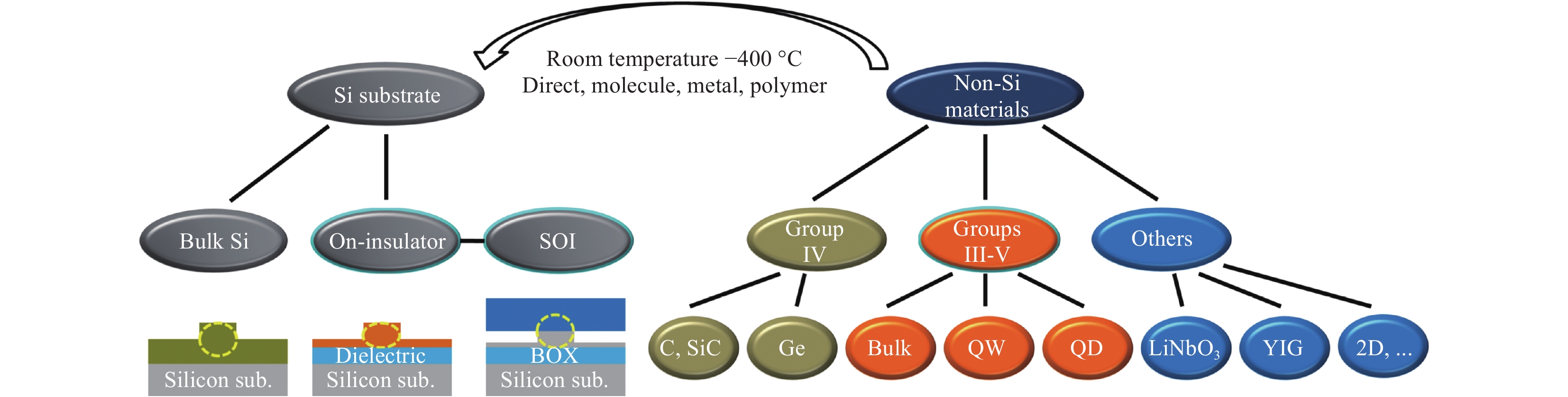
Fig. 1
Schematic overview of heterogeneous Si photonics and its developing branches. Inset: cross-sectional cartoon of three basic waveguides enabled by heterogeneous integration.More generally, we can categorise heterogeneously integrated, optically functional thin-film materials as 1) III-V compound semiconductors as the main stream choice, where we further differentiate them by quantum confinement in the active region, that is, bulk, quantum well (QW), and quantum dot (QD) materials; 2) certain Group IV element semiconductors and compounds, such as Ge28, diamond (C)29, 30, graphene (C)31, and SiC26, 27; and 3) other exotic materials including LiNbO332, which has been widely used in its bulk form to build discrete components owing to its excellent electro-optic effect, and more specialised materials, such as magneto-optic YIG materials for optical isolation33-35, and 2D compounds, for example, MoS2 and ReSe236.
-
Compared with direct epitaxial growth, wafer bonding offers a more versatile and flexible way to integrate similar and dissimilar materials from the perspective of the materials system, size, and processing simplicity. The three required success ingredients of being flat, smooth, and clean are relatively trivial to today’s semiconductor processing technology, regardless of the manufacturing stage37. Thus, wafer bonding has found extensive use in wafer manufacturing, front- and back-end processing of chip packaging in microelectronics, photonics, MEMS, etc38. Because various definitions exist in the literature, we categorise general wafer bonding processes as involving direct, molecular, metal, and polymer bonding based on the type of interfacial material. This sequence is also a function of the mating material proximity and sensitivity to surface roughness and cleanness. Direct bonding refers to mating two hydrophobic material surfaces to eventually form direct covalent bonds between native atoms from both materials, that is, Si-Si. Although it is possible to drive electrical carriers across the interface, it is rarely used in heterogeneous bonding because of the vigorous requirements in terms of the surface conditions, high annealing temperatures (>500 °C) to ensure strong bonds, and similar lattice mismatch issues, commonly encountered in heteroepitaxy39. Molecular bonding mates two hydrophilic surfaces to form strong covalent bonds with the assistance of interfacial foreign atoms, for example, Si-O-In and Si-O-P in InP-to-Si bonding40, 41. This interfacial foreign layer, which mostly consists of dielectrics such as SiO2, SiNx, and Al2O3, is the result of polymerisation reactions involving the -OH dangling bonds on the surface of the native oxide, or a purposely formed oxide via oxidation, wet or plasma surface treatment, dielectric deposition, etc. This layer can be as thin as a few nanometres, but is essential to form strong covalent bonds at low annealing temperatures41, 42, improve immunity to surface roughness and cleanness43, reduce surface topography requirements, and create novel structures with specific optical functionality, for example, a metal-oxide semiconductor (MOS) capacitor44. A problem that commonly occurs in molecular bonding is the trapping of gas by-products, for example, H2 and H2O, from polymerisation reactions at the bonding interface, which causes large voids or a large number of small voids that result in defective device operation37, 45. Known solutions to these problems are high-temperature annealing, dedicated outgassing facilitation structures on the mating surface43, special surface preparation46, and a thick interfacial (porous) dielectric material. On the other hand, efficient electrical carrier transport across the interfacial dielectric is impossible, and thicker dielectrics become a thermal barrier between two semiconductor materials. Metal bonding, including eutectic bonding and thermo-compression bonding, becomes an effective remedy if these two factors are desired47. However, the associated pitfalls are optical absorption, potential metal diffusion/contamination, and post-bonding fabrication inconvenience. Thus, metal bonding is more frequently employed at the chip packaging stage. Polymer bonding, also known as adhesive bonding, is another popular technique in heterogeneous photonic integration48-50. It is the most straightforward ‘glue’ method available and is highly tolerant to surface roughness and cleanness, allowing easy adoption in academic labs for quick device concept demonstration51. Polymer bonding can easily planarise the wafer surface topography and provide protection to patterned features. Interfacial polymer layers less than 50 nm thick have been demonstrated52. However, polymer thickness uniformity, post-bonding process compatibility, and long-term stability are factors to consider in large-scale commercial development. Regardless of the bonding method, thermal annealing at an elevated temperature is necessary to form a strong bond. This is a critical step in heterogeneous integration because of the different material coefficients of thermal expansion (CTE), for example, the linear CTE of Si: 2.6 × 10⁻⁶/°C, InP: 4.8 × 10⁻⁶/°C, and GaAs: 5.7 × 10⁻⁶/°C. Once the native substrate of the transferred thin film is removed or thinned after thermal annealing, all thermal strains concentrate on the thin film (typically <3 μm), hence the maximum annealing temperature is less than 400 °C in most cases to maintain material integrity and minimise doping diffusion41. Other factors such as mechanical pressure and the thermal annealing environment depend on the particular situation. The production of mature SOI wafers as large as 300 mm and high-quality InP-to-SOI bonding of wafers as large as 150 mm proves that wafer bonding can be used in a large wafer-scale process53, but die-to-wafer bonding is economically more viable when the Si substrate is larger than 150 mm and heterogeneous integration entails only a portion of the finished product17, 52, 54.
Definition and overview of heterogeneous silicon photonic integration
Overview of wafer bonding technique in heterogeneous material integration
-
The first electrically pumped heterogeneous laser on Si was a joint research effort of academia and industry with government support14 at a time when industry had been actively looking for solutions of light source integration on Si for quite some time. This timely momentum and accelerating development enabled the successful debut of the first commercial heterogeneous products by Intel in 2016.
Two of the modules in Intel’s 100 Gb/s transceiver product family, PSM4 and CWDM4, are based on heterogeneously integrated O-band DFB lasers55. Intel’s 300 mm heterogeneous production line is used for the entire post-bonding InP-based III-V processing along with the front-end fabrication of high-speed Mach-Zehnder interferometer (MZI) modulators, including passive components including high-resolution photolithography-defined Si gratings. Fig. 2a shows a schematic of the CWDM4 transceiver, where four individually transferred multiple quantum well (MQW) thin films support the consistent and efficient continuous-wave (cw) operation of four single-wavelength lasers. The four wavelengths, which ranged from 1290 to 1350 nm spaced 20 nm apart, constitute a tight wafer-level distribution with a standard deviation of 0.3 nm. Low relative intensity noise (RIN) below –150 dB/Hz and a high side-mode suppression ratio (SMSR) of 50 dB enable a reaching distance of as much as 10 km with single-mode fibre. Laser output power in excess of 20 mW and wall plug efficiency over 15% are achievable with an injection current of less than 100 mA at 80 °C. Devices are able to operate at 150 °C and produce over 2 mW output at an injection current of 180 mA, demonstrating impressive robustness for uncooled operation. Optimized laser MQW epitaxial structures and advanced thermal management solutions have eliminated the negative impact of the previously identified thermal barrier consisting of a thick buried oxide layer (BOX) in SOI substrates56, 57.
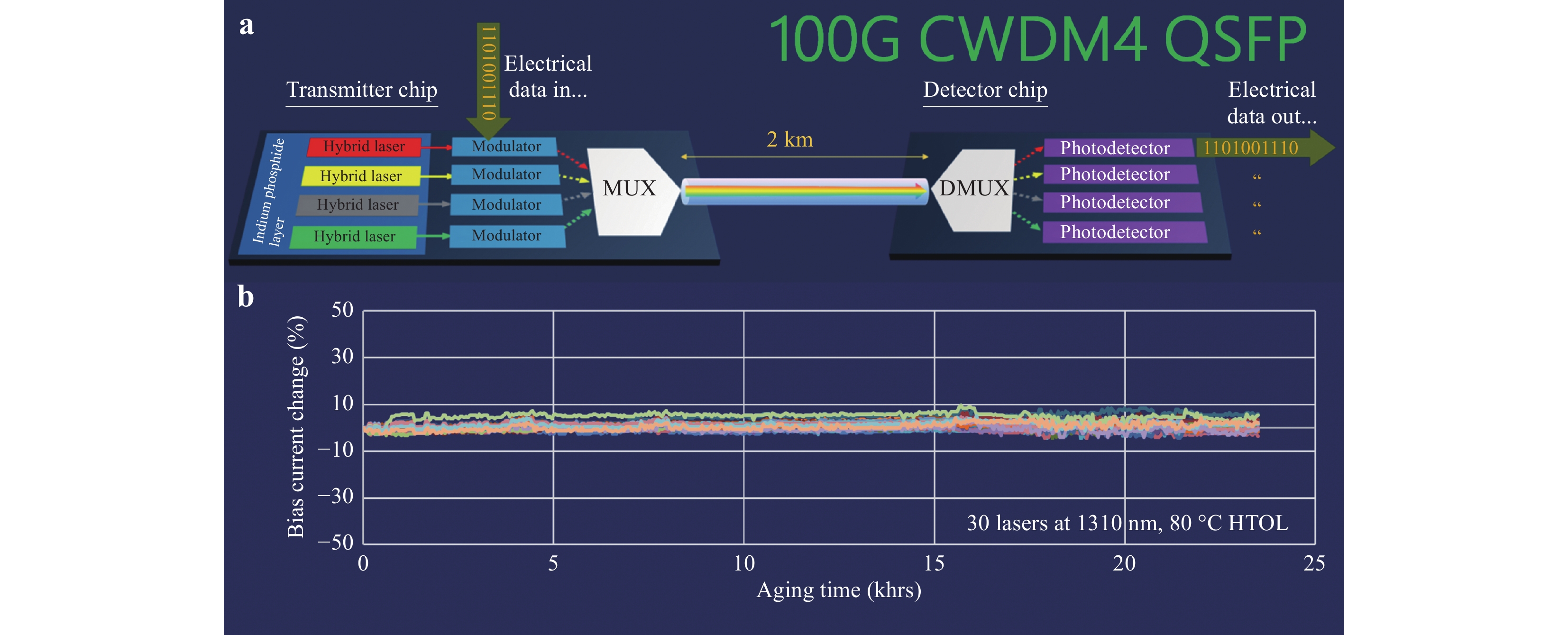
Fig. 2
a Schematic of Intel’s CWDM4 Transceiver solution using four heterogeneous O-band lasers, and b typical HTOL results for 30 such lasers at 80 °C55.Reliable operation is another prerequisite for uncooled operation, and for Intel to ship over one million transceiver units annually55. Fig. 2b shows the high-temperature operating life (HTOL) test on 30 randomly selected 1310 nm heterogeneous DFB lasers at 80 °C under a stress current twice as strong as the specified product operation current. Less than 10% drift of the bias current was required to maintain constant 10 mW output power during the 23,500-hour test, indicating no intrinsic stability concern in heterogeneous integration and excellent quality control in 300 mm wafer-level manufacturing. This qualification outcome was a major concern for many people. The same heterogeneous platform easily hosts a CWDM8 transceiver prototype using eight similar DFB lasers from 1270 to 1410 nm with the same 20 nm ITU grid for 200 or 400 Gb/s applications55, 58. Product extension from pluggable to co-packaged optics59, 5G wireless fronthaul communications60, and Lidar61 extensively rely on reliable on-chip light sources. By the end of 2018, Intel’s market share of Si photonics increased to more than 50% according to the consulting firm Yole Développement62. Heterogeneously integrated light sources are a critical technology differentiator to set Intel’s Si photonics apart from that of other major players who still use off-chip light source solutions or package the finished III-V diode laser chips with Si photonic chips in a conventional hybrid integration fashion. A mature 300 mm scale heterogeneous platform fulfils the promises of superior light engine enablement, larger integration density, a simplified overall packaging effort, and efficient volume production, all of which are designed to reduce costs.
Aurrion was another technology pioneer for commercializing heterogeneous Si photonics and was acquired by the Juniper Network in 2016. On-chip light sources are heterogeneously integrated with data modulation and detection, which are also implemented by individually optimized III-V thin films on the same chip63. In 2015, a fully heterogeneously integrated CWDM4 transmitter including tunable single-wavelength lasers, electroabsorption modulators (EAMs)64, and wavelength multiplexer with a co-packaged CMOS driver chip was demonstrated to deliver a 112 Gb/s non-return-to-zero (NRZ) signal with 10 pJ/bit energy efficiency and a 10−12 bit error rate (BER)65. Efficient lasers and precise wavelength locking in the 20-80 °C range validated the promise for uncooled operation as well66. Compared with selective epitaxy in monolithic integration, flexible bandgap engineering in each active building block is another distinct advantage of heterogeneous Si photonic integration. Different III-V thin films offer superior individual properties in each function: strong optical gain for lasing and amplification, efficient electro-optic effect for modulation and broadband absorption, and efficient detection. A certain degree of associated fabrication complexity is inevitable, but an identical InP-based material system overcomes many challenges, such as that it has the same metallization and passivation steps. More recently, the company showcased their 100 and 400 Gb/s pluggable products and extensions to co-packaged applications67.
Despite the unambiguous advantage of combining the unique strengths from different materials on one large-scale Si wafer, the concept also prevents easy adoption by pure CMOS production foundries unfortunately. Firstly, several widely used ohmic contact metals, for example, Au and Pt, in III-V photonics are strictly forbidden in the CMOS production line. This constraint was eliminated after the successful development of CMOS-compatible ohmic contact metals68. However, many elements in III-V materials are standard dopants for CMOS microelectronics, thus dedicated processing tools plus associated drainage and exhaust systems are necessary to avoid cross-contamination. On the other hand, the current Si photonics wafer volume is still only a fraction of CMOS microelectronics, offering little incentive for CMOS foundries to invest in enormous non-recurring engineering (NRE) efforts to implement drastic changes in their processing and product/process development kit (PDK). Intel’s success in terms of their long-term dedication and vertically integrated business model has proven the technological feasibility, application versatility, and appreciable investment return of large-scale heterogeneous III-V-on-Si photonic integration. Several CMOS-fabless companies including Hewlett Packard Enterprise, Nexus Photonics, Morton Photonics, Nippon Telegraph and Telephone (NTT), and SCINTIL Photonics, are developing proprietary heterogeneous integration technologies. Local government support offsets certain of their NRE expenses. Additional CMOS foundries are also seriously considering expanding their capability to the space of heterogeneous integration. A more inclusive, horizontally integrated ecosystem is on its way to being established with growing market demand, greater industrial and governmental support, and dedicated efforts from players in various stages of the supply chain.
-
Parallel to commercializing the first generation of heterogeneous innovation, primarily the InP-on-Si platform for pluggable optical transceivers used in data centres and high-performance computing, R&D continues to thrive on expanding the spectral coverage and developing novel device structures for broader and emerging applications. One obvious motivation is to expand beyond the 1310 and 1550 nm telecom windows. This is naturally accomplished by physically mating and optically coupling appropriate materials with respect to the spectral window of interest. In other words, transparent passive waveguiding materials are selected for combination with the Si substrate and active thin film materials with the appropriate band gap/epitaxial structure on III-V to develop an efficient active–passive optical coupling.
Silicon nitride (SiNx) has gained significant interest in the past ten years to challenge the dominant role of Si in the light propagation medium on Si substrates, particularly in scenarios where data modulation and detection are not strictly required. SiNx waveguides are attractive owing to their extremely low propagation loss, for example, 0.045 ± 0.04 dB/m in the low-confinement case69, and 0.13 ± 0.05 dB/m in the high-confinement case70, extremely large transparency window extending from visible to mid-infrared (MIR), medium refractive index ~2 for a good balance of compactness and sensitivity to fabrication imperfection, and favourable nonlinear characteristics71. A SiNx/SiO2/Si substrate structure serves as an ideal platform to extend heterogeneous Si photonics beyond the 1.1 μm cutoff line in Si for new applications in displays, AR/VR, metrology, spectroscopy, biomedical, sensing, quantum processing, etc. The shortest wavelength laser that has been heterogeneously integrated on Si72, 73 thus far adopted a vertical optical coupling scheme74, 75. As shown in Fig. 3a, a ‘half’ InGaAs-based 855 nm vertical cavity surface emitting laser (VCSEL) epitaxial structure was transferred onto a special dielectric-on-Si substrate by polymer bonding. The dielectric-on-Si substrates are composed of a 300 nm thick SiNx layer sandwiched between SiO2 cladding above 20 pairs of Ta2O6/SiO2 dielectric, which serves as the bottom distributed Bragg reflector (DBR) mirror for vertical directional lasing. A weak intra-cavity diffraction grating was patterned prior to bonding and resided inside the VCSEL cavity to tap off light into the in-plane SiNx waveguide. The grating was designed to enable a TE-polarization favoured intra-cavity grating/dielectric DBR combination with higher reflection and lower coupling, that is, mirror loss, into the SiNx waveguide. The III-V top DBR was covered by 100 nm Au to further suppress vertical emission. A 1 mA threshold and fibre-coupled bi-directional emission up to ~75 μW each were obtained in Fig. 3b owing to the grating symmetry with respect to the vertical FP lasing cavity. Fundamental transverse mode lasing at 856.5 nm was observed. Suppression of approximately 30 dB to higher order transverse modes is much more effective than conventional VCSEL designs without an intra-cavity grating because higher-order modes contain spatial frequency components with larger off-normal angles than the fundamental mode73.
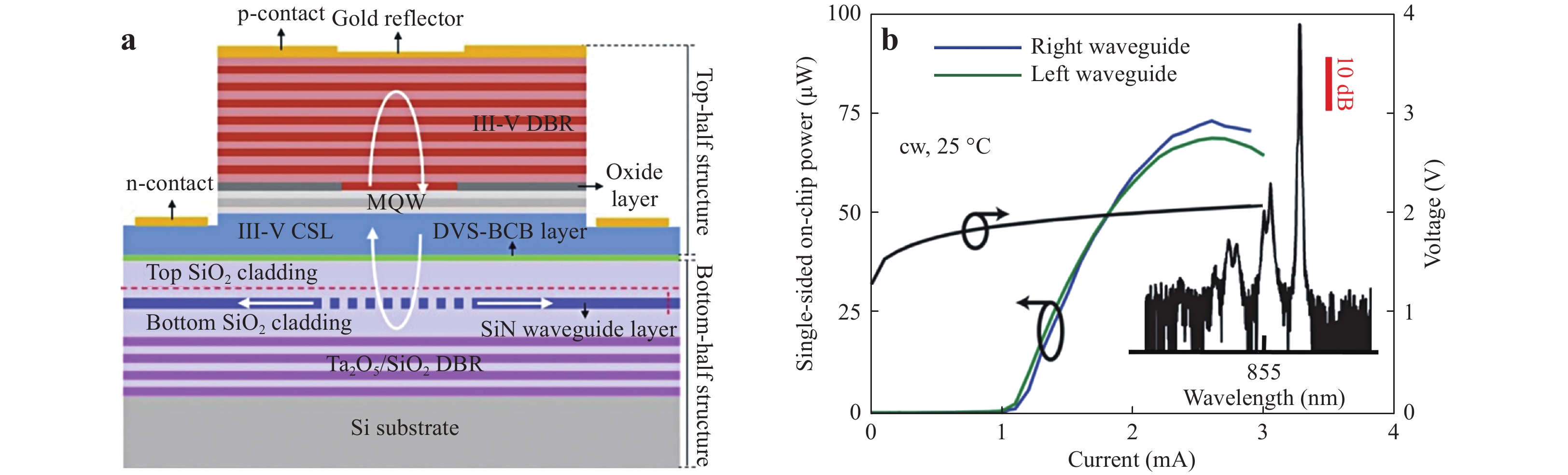
Fig. 3
a Cross-sectional schematic of VCSEL with in-plane out-coupling into a SiNx waveguide, and b device light-current-voltage (LIV) characteristic showing symmetric coupling to the waveguides on the right and left and cw lasing at 856.5 nm73.More recently, a λ = 900 nm in-plane heterogeneous laser and photodetector were also developed by using molecular bonding to enable the GaAs-based gain medium onto the SiNx routing waveguide76, 77. Fig. 4a shows scanning electron microscopy (SEM) images and a simulated fundamental TE mode image of the 350 μm-thick SiNx passive waveguide and ~2 μm-thick GaAs active rib waveguide. A non-disclosed proprietary coupling scheme was implemented to overcome a large refractive index difference of over 1.5 between the SiNx and GaAs materials and allowed a coupling coefficient of as much as 70% in the experiment and over 90% in the case achieved by simulation. Efficient coupling is enabled without the need to use thin layers in the high-index region or prohibitively narrow taper tips to match the modes and their effective indices. The novel design concept and efficient coupling could be applied to GaN/InGaN material system for realizing visible lasers on Si in the future. Fig. 4c shows a top-view SEM image showing InGaAs multiple QWs-based lasers coupled to a SiNx waveguide and routed through an S-bend to an on-chip waveguide-coupled GaAs monitor photodetector (PD). The temperature-dependent light-current (LI) characteristic in Fig 4b shows a robust operation between 20 and 100 °C, benefiting from the larger band gap in the laser-active region. An output power of 10 mW was obtained for a 200 mA injection current at 20 °C. The spectra in Fig. 4b inset show the typical Fabry-Perot (FP) lasing characteristic, indicating the potential to develop more advanced laser cavities on this platform76, 77.
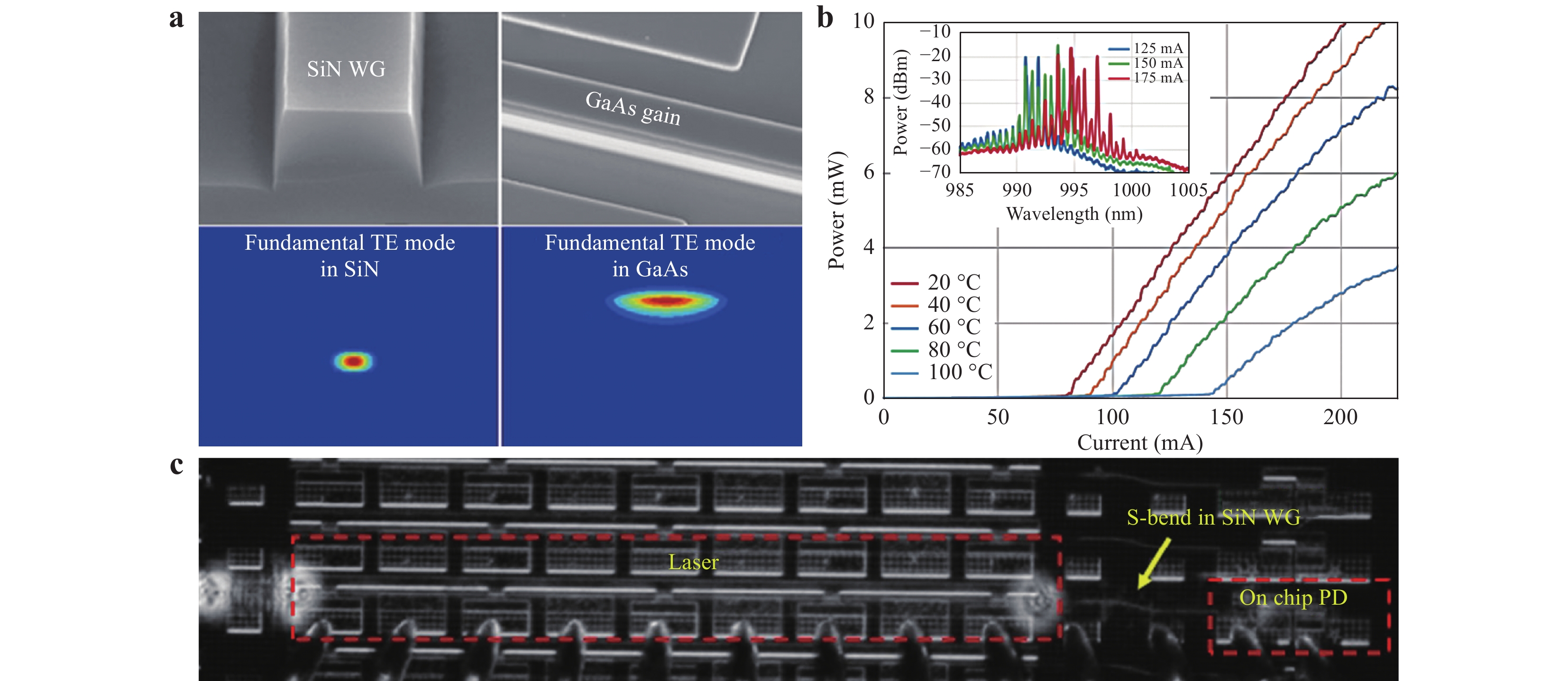
Fig. 4
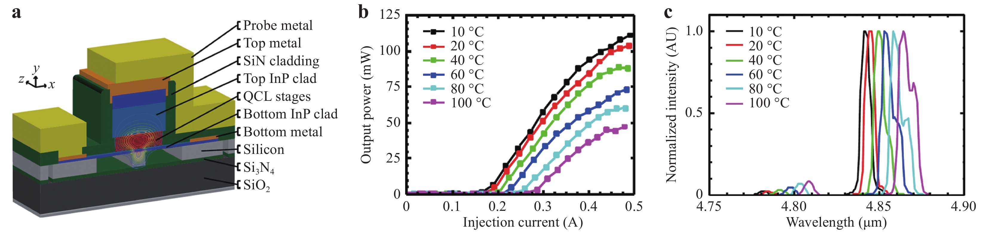
a SEM images of fabricated SiNx and GaAs waveguides and their respective fundamental TE mode profiles, b temperature-dependent LIVs and room-temperature spectra at different injection currents, and c top-view microscopic image showing the integrated laser, passive SiNx waveguide, and PD77.On the other side of the spectrum, heterogeneous lasers with the longest wavelength at 4.8 μm were built by combining a quantum cascade laser (QCL) gain medium with a special Si-on-nitride-on-insulator (SONOI) substrate78. Si is optically transparent to 8 μm, whereas significant absorption in the BOX layer starts at approximately 4 μm79. The solution here is to use a 1.5 μm-thick top Si device layer and insert a layer of 400 nm-thick SiNx above the 3 μm-thick BOX layer such that the optical mode has minimal overlap with lossy SiO2. This platform can be readily employed to support ultra-broadband photonic integration from 350 nm to 6.5 μm80. Such heterogeneous III-V-on-SONOI layer stacks were prepared by depositing SiNx on a SiO2/Si substrate, followed by transfer of the top Si device layer from another regular SOI wafer using molecular bonding. Then, the distributed feedback (DFB) grating with a 1/4λ shift in the centre and Si waveguide were defined prior to transferring the QCL epitaxial thin film. Fig. 5a shows a schematic of the finished device after post-III-V bonding fabrication, where more than 70% of the fundamental TM lasing mode overlapped with the active region of the 30-pair InGaAs/InAlAs superlattices81. As shown in Fig. 5b, output powers of more than 100 and nearly 50 mW were measured under pulsed current injection at stage temperatures of 10 and 100 °C, respectively82. The conservatively designed 3 μm-thick BOX layer and 400 nm-thick SiNx prevented efficient thermal dissipation and cw operation. The corresponding threshold current densities are 1 and 1.59 kA/cm2. The wavelength shift of 0.25 nm/°C in Fig. 5c corresponds to the expected DFB lasing modal change instead of the gain peak shift. A multi-wavelength heterogeneous QCL DFB laser array with an array waveguide grating (AWG) at similar wavelengths was also demonstrated83. Numerous demonstrations based on different III-V thin film selections have been reported to cover light generation, amplification, and detection in the range of –2 to +4.5 μm for a variety of MIR applications84-90.
-
Innovations in heterogeneous materials and device engineering provide critical active functionalities that are inherently lacking in Si and extend the useful spectral window, as discussed above. Recently, the lower loss of silicon waveguides combined with heterogeneous materials has pushed device performance well beyond the abilities of their monolithic counterparts. A narrow-linewidth laser on Si is such an example that is progressing rapidly. The Lorentzian linewidth, that is, the Schawlow-Towns linewidth91 or intrinsic linewidth, is typically referred to as the ultimate, quantum noise-determined laser linewidth limit92. Quantum noise in diode lasers is caused by random spontaneous emission contamination into stimulated emission via photon field intrusion (phase noise Δνφ) and photon-carrier balance disturbance (frequency noise ΔνN). A modification of the Schawlow-Townes-Henry equation for the Lorentzian linewidth Δν 92-94 is shown in Eq.1 below:
$$ \Delta v=\Delta v_{\varphi}+\Delta v_{N}=\frac{R_{s p}}{4 \pi n_{p}}+\frac{R_{s p}}{4 \pi n_{p}} \alpha_{H}^{2} $$ (1) where αH is the linewidth enhancement factor, an important material-dependent parameter that represents the relationship between the imaginary and real parts of the refractive index95. Rsp and np represent the spontaneous emission rate coupling to the lasing mode and the total number of photons stored in the cavity, respectively. A more intuitive expression from the physical laser cavity design perspective is obtained by rewriting Eq. 1 as Eq. 292:
$$ \Delta v=\frac{\pi h v^{3} n_{s p}}{P Q_{E} Q}\left(1+\alpha_{H}^{2}\right) $$ (2) where h is Planck’s constant, ν is the laser frequency, nsp is the population inversion factor, P is the total laser output power, and Q (QE) is the loaded (external) quality factor of the laser cold cavity. The two quality factors here are directly correlated to the internal cavity loss and mirror loss. Therefore, the reduction of absorption in the laser active region and doped regions, passive waveguide loss, and mirror loss, all of which are quantified in a distributed manner through the entire cavity, are effective ways to realise a narrow laser linewidth.
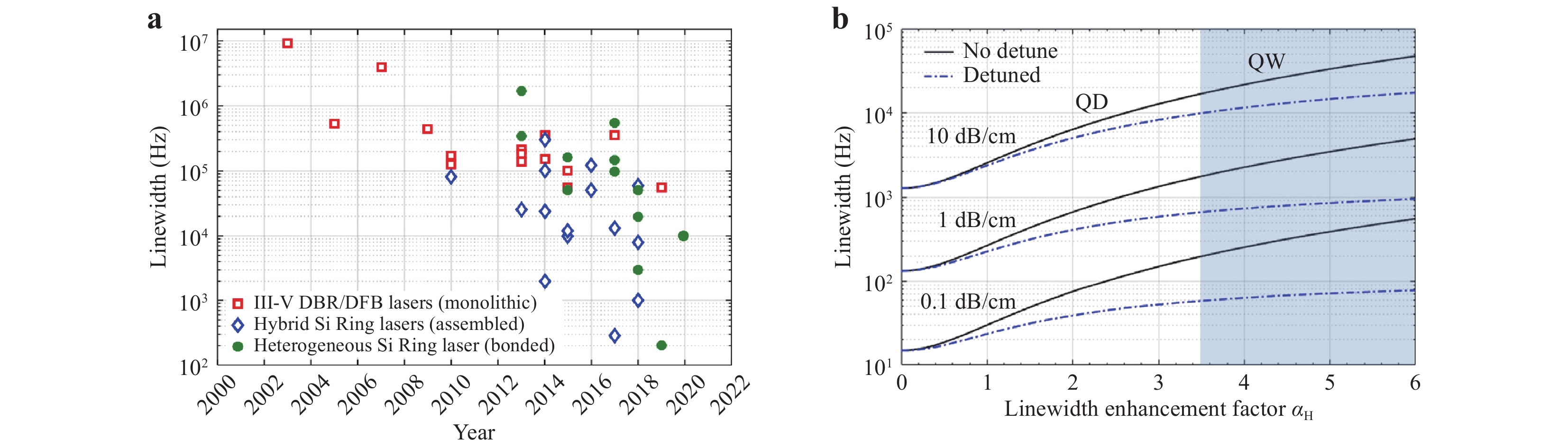
Vertical optical confinement factors for III-V active region and doped layers in heterogeneous platforms can be conveniently engineered by adjusting the Si waveguide dimension, III-V epitaxial structure, and proximity in between16. As shown schematically in Fig. 6c, a 150 nm-thick SiO2 spacer between Si and III-V resulted in >95% lasing modal confinement in low-loss Si, 1.5% in III-V, and only 0.2% in QW96. In addition, a 1D photonic band gap engineered high-Q (~106) laser cavity in Fig. 6a introduced another layer of loss reduction. A Si grating section (Ld) with a varying grating groove width in the transverse direction created parabolically modulated frequency band edges along the mode propagation. Thus, the lasing mode can be localised tightly in this potential well ‘V’ with minimal coupling loss to the radiation modes. A shallow Si rib waveguide was also purposely designed to minimise scattering from the etched sidewalls. A Lorentzian linewidth of approximately 1.1 kHz with amplifier noise included was measured in this solitary heterogeneous DFB laser96, representing a linewidth reduction of 600× relative to the best monolithic III-V counterpart.
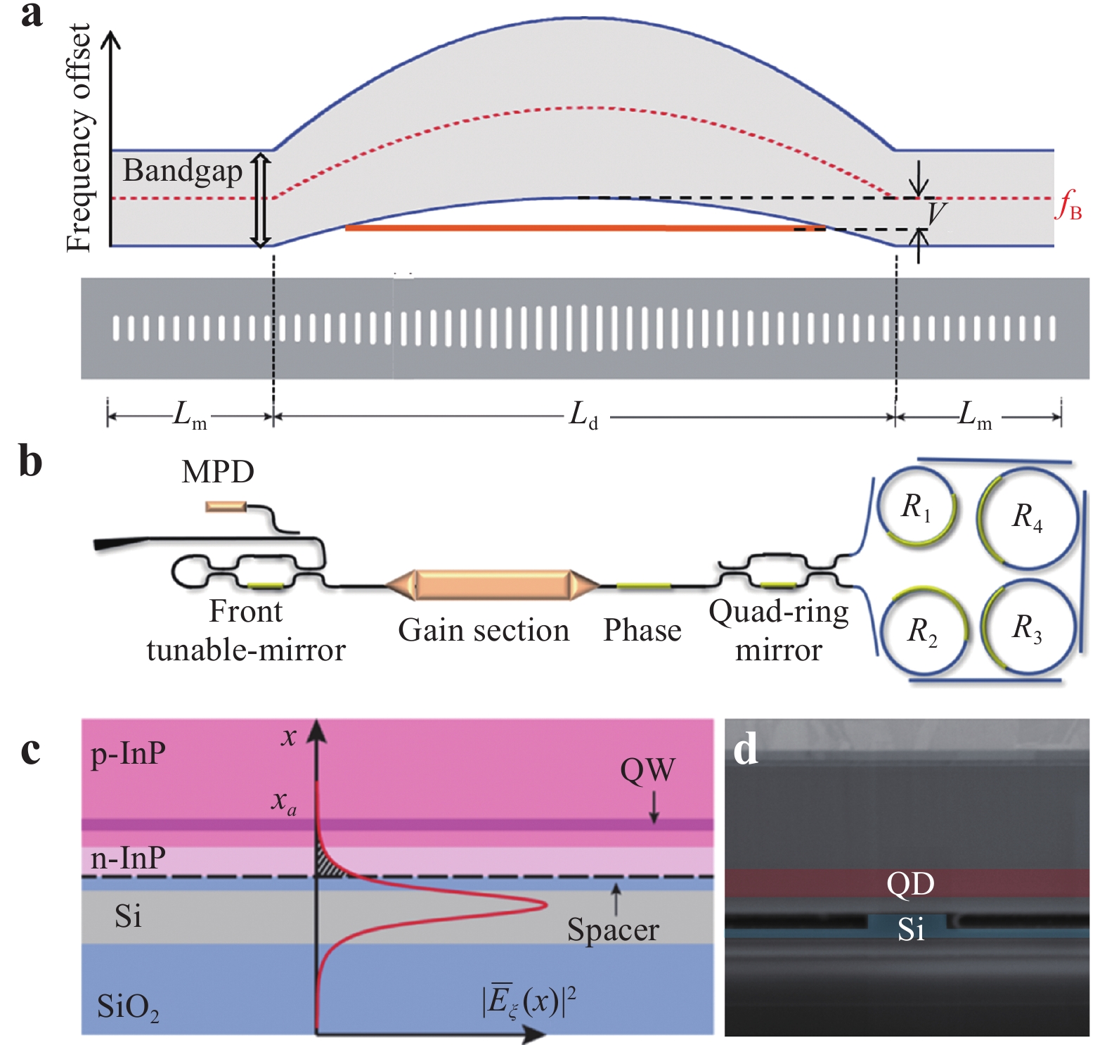
Fig. 6
a Schematic photonic band gap structure and top-view of the high-Q grating-based laser cavity geometry in96 and c its heterogeneous cross-sectional schematic with lasing mode profile, b schematic of a MQW-based heterogeneous extended cavity laser structure92, and d SEM cross-sectional image of a similar QD-based extended cavity laser105.In contrast to the solitary design, where the distributed internal cavity loss remains independent of the total cavity length, extended/external cavity design can effectively reduce the longitudinal optical confinement factor to absorptive III-V thin film by extending a large portion of the laser cavity to lower-loss Si (e.g. 0.16 dB/cm for a quasi-single mode waveguide97) or a much lower-loss SiNx waveguide98-100. Therefore, both distributed internal and mirror losses are reduced as the laser cavity extension. Further leverage of the detuned loading or optical negative feedback effect101 in designs with narrow mirror reflectivity bandwidth can dilute the negative impact of the linewidth enhancement factor αH. Without providing the details, one can comprehend detuned loading as an elegant way to build negative/favourable or positive/undesired feedback by setting the lasing frequency at a negative or positive detuned side with respect to the frequency at the maximum mirror reflectivity. Lasing frequency perturbation triggers a chain of events that affects the reflectivity, photon density, carrier density, refractive index, which are fed back to the lasing frequency. A negative feedback loop has been proved to be of great use to stabilise the lasing frequency and suppress quantum noise from the QW gain medium102. Because the αH factor is typically 2-5 for the QW structure (>3 in most of our devices) 95, 103, 104, this effect becomes a significant advantage over solitary lasers in which the Lorentzian linewidth scales with (1 + αH2) according to Eq. 1. Choices such as single-frequency Bragg gratings, sampled gratings, high-Q ring resonators, or a combination of them serve well as this extended passive section. High-Q ring resonators are particularly attractive for three reasons. Firstly, a high-Q ring resonator with a long photon lifetime at resonance frequency is analogous to the optical delay lines but with a much smaller physical footprint. Secondly, their extremely narrow bandwidth offers excellent spectral purity over a broad range. Finally, single or multiple coupled rings enable wide spectral tunability with low tuning power consumption. Fig. 6b illustrates such an extended heterogeneous laser design, where a coupled-quad ring structure was designed as the back mirror102. More than two coupled rings in this design help alleviate the trade-off between insertion loss and spectral bandwidth, both governed by the ring coupling coefficient. Therefore, the overall Q of the cavity can be enhanced without overly sacrificing the coupling coefficient102. At an output power of approximately 2 mW, optimal control of the gain section and rings with respect to the detuning loading effect led to the narrowest Lorentzian linewidth of 140 Hz at an emission wavelength of 1565 nm that was known at the time. The same device also exhibited impressive 120 nm-wide wavelength tuning from 1484 to 1604 nm 102.
If large spectral tunability is not required, a high-Q single-frequency Bragg mirror based on a low-loss waveguide is a much simpler choice. Xiang et al. recently fabricated a heterogeneous laser in the C-band using a 20 mm-long on-chip SiNx spiral-shaped DBR as the back mirror100. Except for the SiNx/Si taper region, the SiNx strip waveguide DBR was completely surrounded by SiO2 without Si and the III-V thin film above. This resulted in a highly thermally stable wavelength of 10.46 pm/°C, more than 7× smaller than that of a typical one with Si-based mirrors. A Lorentzian linewidth of 4 kHz was measured despite design and fabrication imperfection in the first run100.
We note that the detuned loading effect is a ‘double-edged sword’ capable of demolishing or amplifying the impact of the αH factor to cause subsequent linewidth reduction or broadening, depending on whether detuning of the lasing frequency with respect to the central frequency of the maximum mirror reflectivity is negative or positive. Thus, accurate and careful lasing frequency control is critical and challenging in practical applications with variable environmental factors. A trade-off between laser efficiency and lasing frequency detuning is also inevitable92. Another straightforward solution, particularly in heterogeneous integration, is to use a quantum dot (QD) gain medium instead. The αH factor of QD materials was experimentally and theoretically proved to be as low as zero or even negative106, 107. The αH factor in QD materials, which ranges from very small to zero, originates from their symmetrical gain spectrum108 and is strongly affected by dot uniformity and doping density107. A αH factor of approximately 1 was measured using an InAs/GaAs QD-on-Si heterogeneous laser109, 110, where the InAs/GaAs QD active region was not optimised towards a zero αH factor. A similar heterogeneous extended cavity laser based on a dual-coupled-ring reflector design and the same QD gain medium highlighted in the cross-sectional SEM image in Fig. 6d was fabricated recently for the first time105, 111. A minimal Lorentzian linewidth of 5.3 kHz was extracted from the measured white noise upper limit of 1.68 kHz2/Hz at approximately 1310 nm, indicating a nearly 10× improvement over previous O-band laser record, also from a heterogeneously integrated QW-on-Si laser112.
Fig. 7a shows the historical progress of Lorentzian linewidth reduction in diode lasers with different integration formats92. It is clear that progress in conventional III-V QW lasers started levelling off 10 years ago because of the fundamental properties of materials and design limits of external and solitary laser cavities on the III-V monolithic platform. However, in the past decade, a linewidth reduction of four orders of magnitude enabled by hybrid and heterogeneous platforms once again resulted in tremendous advancement because parameters such as Q, QE, and αH could be improved instantly and independently. As projected in Fig. 7b, the transition from the QW to the QD material system benefits from small or even zero αH dot gain medium with the largest and most straightforward impact without the complexity of accessory device design. Cavity loss reduction is of secondary significance, but is also effective, as the resulting linewidth reduction almost occurs at the same pace as loss reduction. A sub-100 Hz linewidth is expected to be within reach when low-αH QD materials are coupled with the design of distributed cavity loss as low as approximately 0.1 dB/cm. The effect of dilution on the αH factor by detuned loading is more potent for materials with large αH, that is, the QW gain medium. Diode lasers with such a narrow linewidth would be anticipated to have unprecedented impact in coherent communications and sensing, metrology113, microwave photonics114, etc.
-
In addition to frequency noise suppression or elimination, a low or zero αH factor in QDs largely raises the critical external feedback level for coherence collapse in diode lasers107, 115-117. Error-free laser operation under 100% external feedback has been shown in QD lasers118, 119, indicating the feasibility of removing bulky and expensive optical isolators in a laser or transmitter package120. Furthermore, 3D band gap structure in QDs provides a complete confinement for injected carriers as well as good crosstalk isolation among dots. This results in low transparency current density121, excellent optical gain thermal stability122, 123, low relative intensity noise (RIN)124, and large tolerance to material and fabrication defects125, 126. Owing to the inhomogeneous dot size distribution commonly seen in widely used Stranski-Krastanov growth method, wide spectral gain bandwidth127 is ideal for broad spectral lasing applications, for example, comb lasers or widely tunable lasers. All these favourable material properties encourage the development of heterogeneous QD comb lasers109 for DWDM communication128, 129, as the current CWDM4 standard with 20 nm channel spacing is becoming a bandwidth scalability bottleneck for post-400 Gb/s direct detection applications in data communications. Fig. 8a shows an FP laser built on this QD-on-Si platform and exhibits robust operation and impressively low cw threshold current density 670 A/cm2 at 100 °C (280 A/cm2, 7% wall-plug efficiency at 20 °C) 130. A minimal threshold current of 165 A/cm2 was recently measured. When adding a saturable absorber (SA) section to the laser cavity with appropriate bias for it and the gain section, four-wave mixing promotes stable mode-locked lasing. A clear multi-wavelength operation with extremely large 3, 6, and 10 dB comb widths of 12, 18, and 25 nm, respectively, as shown in Fig. 8b, is likely the result of the unique combination of spatial hole burning, group velocity dispersion, a linewidth enhancement factor, and four-wave mixing131. The enlarged spectrum in Fig. 8c reveals a channel spacing of 15.5 GHz, that is, the laser free spectral range (FSR), which is inversely proportional to the 2.6 mm-long laser cavity defined by photolithography. This channel spacing varies negligibly with changes in the device temperature. Within this cavity, a 1.4 mm long active section with an SA at the centre employed the same InAs/GaAs QD-on-Si configuration as that of the QD narrow-linewidth laser in Fig. 6d. Over 135 constantly spaced wavelengths within 3 dB power variation were realised from this single comb laser, which is only controlled by three terminals. A large channel spacing (e.g. 100 GHz) can be realised by a multiple-saturable absorber (SA) design or Vernier effect in an extended cavity132 rather than reducing the laser cavity excessively. Compared with the conventional approach to form a multi-wavelength source with a bank of single-wavelength lasers, the comb laser has a clear edge in terms of its footprint, control simplicity, and energy efficiency133. Inherently low RIN in the QD gain medium is critical to obtain high signal integrity in a full link, particularly for PAM4 and the more advanced modulation format. A 10-channel transceiver link based on a heterogeneous comb laser and SiGe avalanche photodetector was recently demonstrated to deliver a conservative aggregated 160 Gb/s error-free NRZ data transmission with an energy bill of 3 pJ/bit134. Current comb laser research focuses on further wall-plug efficiency enhancement and QD mode-locked laser model development. A similar InAs/GaAs QD gain medium has also been used to develop heterogeneous compact low-threshold microring lasers135, 136 and robust DFB lasers137. It is noted that despite numerous desirable material properties, the finite intra-band relaxation time and the gain saturation effect in QDs significantly limit the QD laser direct modulation bandwidth, resulting a bandwidth of only 5-10 GHz for 1310 nm InAs/GaAs QD lasers in general136. Optical injection locking was recently used to extend the bandwidth to more than 20 GHz to support 25 Gb/s NRZ modulation138, 139. The same heterogeneous platform can be expected to allow convenient master and slave co-integration, for example, using a single comb master laser to injection lock a series of microring slave lasers138.
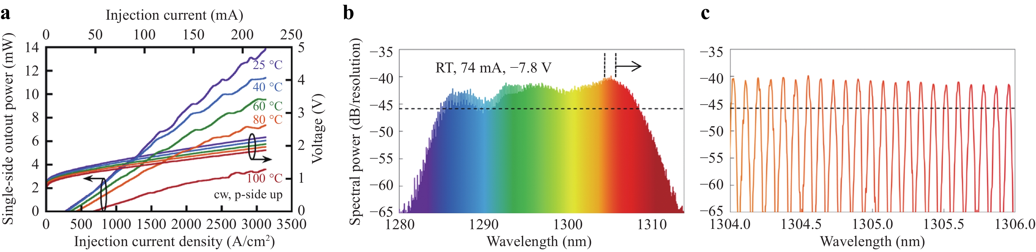
Fig. 8
a Temperature-dependent LIV characteristic of a heterogeneous QD FP laser, b Optical spectrum of the comb laser. b optical spectrum of the comb laser over the full wavelength range, c enlargement of the range indicated in b to show individual lasing modes. The dashed line is drawn at −6 dB from the peak comb line131.Another interesting use case of such heterogeneous QD-on-Si integration is the discovery of extremely low dark current and avalanche gain when reversely biasing the same diode140, 141. A record low 1 × 10⁻⁶ A/cm2 dark current density at −1 V was measured in such a QD photodetector built on the same chip with comb lasers using an identical III-V epitaxial stack and fabrication process. Low crystal dislocation density among electrically isolated dots and well-passivated devices are considered to be the root causes. Because of the strong carrier confinement and small absorption volume, the responsivity is relatively low, for example, 0.1 A/W at −1 V bias for a 90 μm-long device with 1310 nm light as the input. However, a maximum avalanche gain of up to 350 for TM mode and 150 for TE was recently observed at a breakdown voltage of approximately −18 V. The corresponding gain-bandwidth-product is 300, also a record for QD avalanche photodetectors (APD) and comparable to state-of-the-art SiGe and Ge APDs142. Error-free operation at 20 Gb/s in NRZ mode was achieved on such a heterogeneous QD APD, indicating the potential to play the role of a high-speed receiver as well as a monitor PD.
-
Superior active functionalities in III-V materials used complementary with exceptional low-loss passive components in Si, SiNx, or SiO2 have proved to be a success formula in all the cases that have been discussed thus far, but are not the only success. Researchers are actively exploring the nonlinear properties of III-V thin films to enable high-quality heterogeneous passive III-V components on Si to be developed at the present time, and active-passive integration in the near future. The nonlinear coefficients in most III-V materials are usually several orders of magnitude larger than those of popular dielectrics such as SiNx and SiO2143. For example, the nonlinear Kerr index n2 of SiO2, SiNx, GaP and AlGaAs is 3 × 10⁻²⁰, 2.5 × 10⁻¹⁹, 1.1 × 10⁻¹⁷ and 2.6 × 10⁻¹⁷ m2/W, respectively. The mode volume in an HIC III-V-on-insulator waveguide structure is also much smaller than that of its dielectric counterparts. Both factors contribute to a significantly lower parametric oscillation threshold power (Pth) to trigger nonlinear effects, as governed by Eq. 3144, 145:
$$ P_{t h} \approx 1.54 \frac{\pi n w A}{2 \eta n_{2} D_{1} Q_{T}^{2}} $$ (3) where n is the modal index, w is the angular frequency, A is the modal area, η is the coupling factor equivalent to the proportion of (external) coupling loss of the total (internal + external) resonator cavity loss, and QT is the total quality factor of the resonator. D1 equals c/Dng, a function of the resonator diameter D, the speed of light in vacuum c, and the group index ng. A smaller A, much larger n2 and smaller D all favour a III-V resonator despite the higher QT in much larger SiO2 and SiNx resonators70, 146. Furthermore, the third-order nonlinear effect on top of the second-order one in III-V materials enhances its attractiveness for frequency comb generation147. Therefore, AlGaAs/GaAs and GaP emerge as promising III-V thin-film candidates148, 149.
As shown in the inset of Fig. 9a, a 700 mm × 400 nm Al0.2Ga0.8As strip waveguide was fabricated upon transferring a layer of undoped Al0.2Ga0.8As on a SiO2/Si substrate via molecular bonding150, 151. The small mode volume (~0.28 μm2) is 4 × smaller than that of the SiNx counterpart, indicating a lower photon energy and more compact footprint for comb generation. Special care was taken to smooth out line-edge roughness in the photoresist pattern, optimise the III-V dry etch process, and passivate defect states on the III-V surface with 5 nm-thick Al2O3 to achieve an intrinsic quality factor of 1.53 × 10⁶ in a microring resonator with a diameter of 12 μm (FSR=1 THz) (Fig. 9b inset) at approximately 1519 nm25, 150. This corresponds to an extremely low propagation loss of 0.4 dB/cm, 10 × smaller than that of typical III-V waveguides152, 153 and at least 3 × smaller than many reported loss values for Si waveguides of similar dimensions. Lattice-matched AlxGa1-xAs on the GaAs substrate provides the freedom to adjust the concentration of Al ‘x’, i.e. the band gap, for 1) a minimal two photon absorption loss and 2) anomalous group velocity dispersion (GVD)154 at the wavelength of interest, i.e. the C-band in this case. The onset of the frequency comb generation can be observed in the parametric oscillation spectrum of such a 1 THz resonator in Fig. 9a under a low pump power of 36 μW at the C-band. To the best of our knowledge, this represents record-low threshold pump power for comb generation among numerous nonlinear material platforms, for example, a reduction of approximately 100 × relative to previously reported AlGaAs-on-insulator resonators with similar FSR148, and an improvement of 10× compared with their integrated dielectric counterparts150, 154, 155. The higher nonlinear efficiency owing to the high n2 in this case is reflected by the >250 nm-wide spectral range under a pump power of 300 μW, as shown in Fig. 9b, which is also lower than the previous record held by a SiNx micro-comb70. A soliton-step transition has also been observed as a result of the small thermal impact of efficient pumping150. Outstanding performance in frequency conversion was also achieved in a low-loss GaAs-on-insulator waveguide for the same reasons discussed above151. Exceptional normalized second-harmonic efficiency of 13,000% W−1cm−2 at a fundamental wavelength of 2 μm was achieved by harnessing the advantages of a materials platform and an improved fabrication process25, 150.
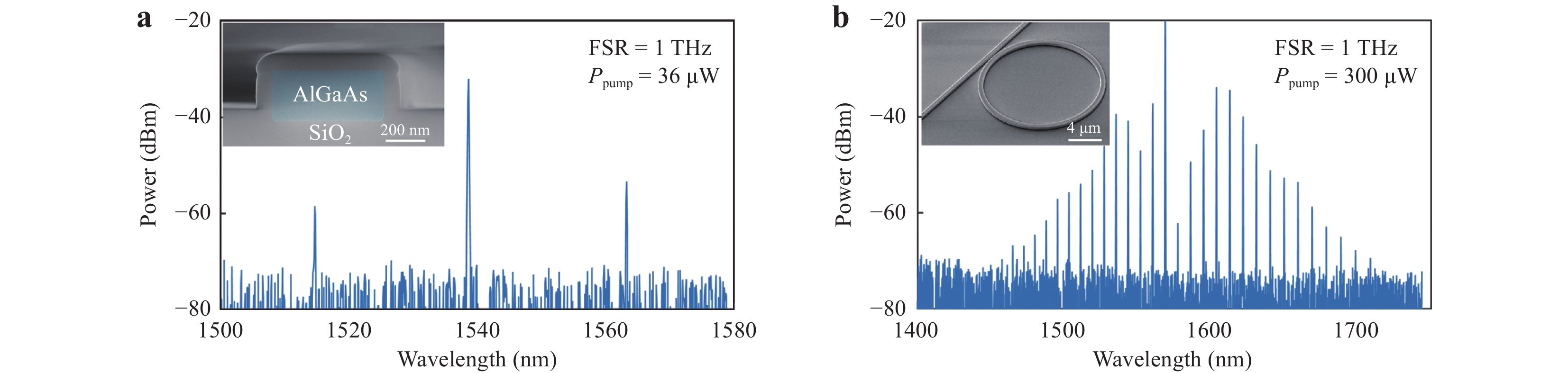
Fig. 9
Measured spectra of 1 THz resonator under pump power of a 36 μW and b 300 μW. Inset. a cross-sectional and b side view SEM images of an AlGaAs resonator150.On-going efforts continue to focus on driving the waveguide loss down to further enhance the quality factor of III-V nano-waveguides. This will be a natural by-product once this platform is scaled up to 200 and 300 mm and processed in a commercial foundry with higher-resolution photolithography and tighter process control. Compared with the SiNx and SiO2 high-Q resonators, we note that another huge potential advantage inherent to high-Q III-V-on-insulator nonlinear components is the compatibility of their materials and process simplicity for many of the heterogeneous active devices discussed before. For example, an InAs/GaAs QD pump laser could be integrated with a high-Q AlGaAs-on-insulator resonator for potentially even lower pump thresholds, and this integration becomes an alternative multiple wavelength source apart from comb lasers. Alternatively, a more sophisticated integration could include tunable narrow-linewidth QD lasers, another high-efficiency QD pump laser, and APD that could be readily integrated with a high-Q AlGaAs-on-insulator resonator to form a fully integrated optical-frequency synthesiser based on the proof-of-concept demonstration using discrete parts113 but on a millimetre-scale chip. Briefly, the superior device performance and large potential for improvement discussed in this section are turning nonlinear optics into another irresistible force to drive heterogeneous Si photonics beyond the traditional optical commutations, and into applications of high-speed optical signal processing, metrology, and quantum communication and computation.
-
The last representative heterogeneous component, but definitely not the least, is a novel III-V/dielectric/Si MOS capacitor for ultra-efficient phase tuning and high-speed modulation156-159. As shown in the TEM cross-sectional image in the inset of Fig. 10a, this heterogeneous capacitor can be conveniently formed by sandwiching a layer of high-quality thin dielectric material, that is, gate oxides such as SiO2 or Al2O3, or even polymer, at the III-V/Si bonding interface during molecular or polymer bonding. When this capacitor is charged or discharged by applying an electrical field between the III-V material and Si, the carrier concentration around the gate oxide can change by several orders of magnitude to exceed 1020/cm244. By designing a ‘staircase’-shaped waveguide of which the optical mode overlaps with this capacitor (Fig. 10b inset), it would be possible to introduce the plasma dispersion effect to manipulate the real and imaginary parts of the modal index based on the Drude model6.
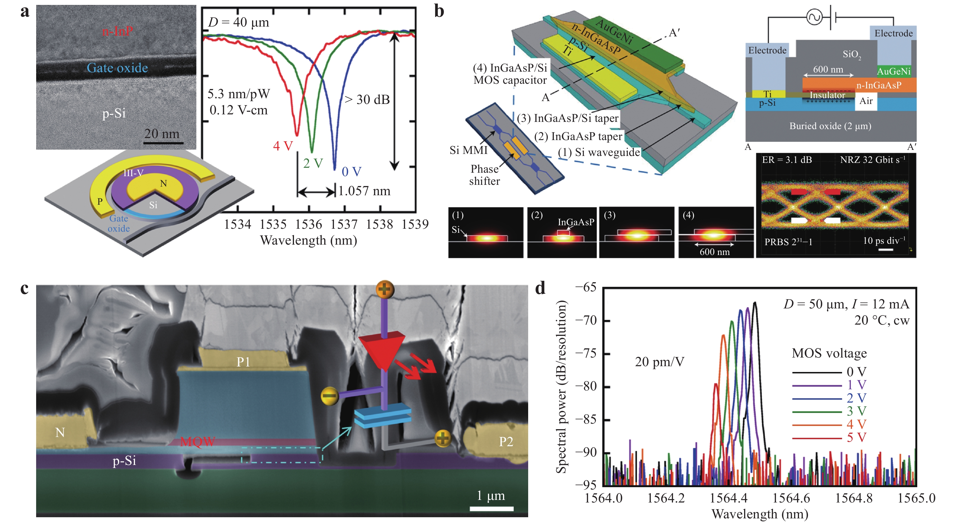
Fig. 10
a Measured spectra of a heterogeneous MOS microring resonator under different MOS bias. Insets: schematic device structure and a cross-sectional TEM image showing MOS capacitor region162. b Schematic device structure and cross-section of a heterogeneous MZI modulator. Insets: simulated mode profile at different waveguide stages and NRZ modulation eye diagram157. c Simplified circuit model and cross-sectional SEM image of a heterogeneous MOS capacitor laser, and d its spectra under different MOS voltages156.Prior to application to heterogeneous MOS devices, the same concept was employed on a pure Si platform to realise the first Gb/s Si modulators160. Because this capacitor (dis)charge process occurs under a fast electric field effect, rapid engineering progress soon led to the development of a decent Si MOS modulator capable of performing 40 Gb/s NRZ modulation161. However, compared with the pure Si design where deposited poly-Si is typically used as the top layer above the gate oxide, a wafer-bonded III-V layer offers three advantages with respect to its material characteristics. Firstly, crystalline III-V material has lower optical loss than poly-Si, even though it is highly doped. Secondly, the much smaller conductivity effective mass of electrons and larger electron mobility in a III-V material results in a larger (smaller) real (imaginary) part change in the modal index, which translates into larger phase change efficiency and lower free carrier absorption, respectively. Finally, the band-filling effect in a III-V material contributes to the phase change in addition to the plasma dispersion effect158. Furthermore, wafer bonding greatly simplifies fabrication by obviating the need for chemical mechanical polishing (CMP), which is typically required before poly-Si deposition in pure Si MOS waveguide formation.
Fig. 10a shows a heterogeneous InP/oxide/Si MOS microring resonator 40 μm in diameter162. The resonator consists of a 12 nm-thick gate oxide layer containing a combination of HfO2, Al2O3, and SiO2 sandwiched between 250 nm-thick p-Si and 150 nm-thick InP layers. Here, high-k HfO2 was selected to enhance the capacitance for a large plasma dispersion effect, and Al2O3 and SiO2 were used to form good interfaces with InP and Si, respectively. A resonance wavelength blue shift in the C-band in excess of 1 nm was obtained by applying bias of 4 V across this capacitor, translating to a tuning pace of 0.26 nm/V and a phase-shift/modulation efficiency VπL of 0.12 V-cm. Because of the extremely low DC leakage current, typically in the fA range44, a record tuning energy efficiency of 5.3 nm/pW was calculated. This is an improvement of nine orders of magnitude over conventional thermal and carrier injection tuning with a few or sub-nm/mW efficiency. The decreasing extinction ratio in the spectra when increasing bias is applied to the MOS capacitor is due to simultaneously rising FCA, which forces the resonator to drift away from the critical coupling condition at a bias of approximately 0 V. Another reported heterogeneous MOS MZI structure exhibited a VπL of 0.047 V cm and 0.23 dB attenuation across the 500 μm-long MOS phase shifter that are 5 and 10× lower than those of a Si MOS modulator, respectively158. This is attributable to the use of thin Al2O3 gate oxide with 5 nm equivalent oxide thicknesses and n-InGaAsP rather than n-InP for a larger (smaller) electron-induced refractive index (FCA) 158. Furthermore, MOS capacitor-enabled phase tuning is also an athermal and much faster process than the two popular methods, making it a more effective phase-tuning mechanism for negligible power consumption, zero thermal crosstalk, higher phase shift efficiency, lower insertion loss, and faster response.
Fig. 10b shows a schematic of one arm of a MOS MZI modulator157. A SiO2 gate oxide layer with a thickness of 10 nm was used to ensure a good trade-off between a small VπL (0.09 V-cm) and large RC time limit for high-speed modulation. Appropriately designed taper structures ensured low-loss transitions and minimal reflection at different stages of light propagation, i.e. an input/output Si strip waveguide, InGaAsP taper, InGaAsP/Si taper and InGaAsP/Si MOS capacitor, and an MOS capacitor phase shifter. Their corresponding simulated fundamental TE mode profiles are displayed in the insets in Fig. 10b. Although the RC-limited 3 dB bandwidth was below 1.5 GHz because of imperfections in the design and fabrication, NRZ signal modulation as high as 32 Gb/s and an extinction ratio over 3 dB in the C-band were achieved with the help of the pre-emphasis drive signal and maximum Vpp of 3.5 V. A much larger bandwidth (as large as 30 GHz in the O-band) was demonstrated in another MZI design by reducing the RC constant with lower series resistance and doubling the thickness of the SiO2 gate oxide layer (20 nm) at the cost of reduced modulation efficiency (VπL = 1.3 V-cm)159. NRZ signal modulation as high as 25 Gb/s was measured by applying a Vpp of 4 V without using a pre-emphasis driving signal. Improved design recently paved the way to relieve the trade-off between modulation efficiency and the RC limit, the primary speed limit for MOS-type modulators163. Excellent temperature insensitivity was also confirmed in these MOS capacitive modulators164. By the time of manuscript preparation, we also developed the first heterogeneous GaAs-on-Si MOS microring modulator with promising NRZ modulation in excess of 25 Gb/s without pre-emphasis in limited preliminary testing165.
All desirable MOS capacitor-enabled functionalities can be easily integrated in heterogeneous III-V-on-Si lasers, which then become a three-terminal configuration as shown in Fig. 10c, which shows a simplified circuit model and a cross-sectional SEM image of the device156. The terminals P1 on p-InGaAs and N on n-InP are the normal diode laser anode and cathode, respectively, to inject carriers into the active region of the MQW. The new terminal P2 on p-Si and the terminal N allow a voltage bias to be applied to the n-InP/Al2O3 (15 nm)/p-Si capacitor. A similar blue-shift in the wavelength as a function of the MOS voltage across the capacitor proves that it is a result of the plasma dispersion effect when the current injected into the MQW is held constant, as shown in Fig. 10d. On the other hand, increasing the FCA loss with higher MOS voltage leads to higher internal cavity loss and, subsequently, a higher laser threshold and lower efficiency. The laser output power was observed to decrease by more than 10 dB when the MOS bias is varied from 0 to 5 V, enabling high-speed frequency modulation and amplitude modulation. A 3 dB MOS modulation bandwidth of 14.5 GHz was measured. This is more than 2× larger than the conventionally preferred direct current modulation bandwidth (6.6 GHz) to the same device with the same DC injection current166. This is because MOS modulation perturbs the internal cavity loss, that is, the photon lifetime, which is a much faster process than injection carrier perturbation167.
This MOS capacitor structure is a direct and unique product of wafer bonding-enabled heterogeneous integration, and is impossible to replicate on a hybrid integration platform. In addition to the excellent optical, mechanical, and thermal properties of Si, this novel heterogeneous MOS capacitor activates the desired and well-studied electrical properties of Si on this heterogeneous platform. A fully integrated DWDM transceiver on Si is being developed to include previously discussed QD comb lasers, MOS microring modulators and drop filters, and QD APDs. The straightforward integration of MOS capacitors in lasers, modulators, and filters can be expected to enable agile wavelength tuning and locking in each channel to correct the laser/microring resonance frequency mismatch due to fabrication imperfection and temperature fluctuation. A single QD epitaxial transfer and a concurrent process to simultaneously fabricate all these key components would also greatly simplify the design and fabrication in comparison with designs that use different III-V epitaxial stacks for different building blocks168.
Spectral extension enabled by heterogeneous integration
Narrow-linewidth lasers on silicon


Quantum dot devices on Si
Heterogeneous nonlinear devices on silicon

Heterogeneous devices with integrated MOS capacitor
-
In this section, we review several platform level innovations that aim to make fabrication more foundry-friendly, further drive the device potential, or import more III-V PIC integration technology to large-scale Si levels. As high-quality CMOS-compatible Si modulators and Ge-based detectors are readily available, heterogeneous lasers/amplifiers are still the only ‘most valuable/wanted player’ in the heterogeneous integration fleet, purely from the perspective of the minimal III-V processing preferred by a CMOS foundry. Therefore, to accommodate many CMOS-compatible materials, for example, Ge, SiNx, etc., and their uneven surface topography and high thermal budget, a new front-end Si photonic process flow was proposed and illustrated in Figs. 11a-c 169-171. The process starts with conventional Si passive component formation on an SOI wafer, and then selectively adds amorphous silicon (a-Si) to certain areas to increase the local Si thickness. All high-temperature processes, such as SiNx deposition, Ge growth, and implantation activation, can be included in this stage. Upon SiO2 encapsulation and surface planarization, the entire device function-ready layer is transferred onto an oxidized Si handle wafer by a molecular bonding process followed by selective removal of the Si substrate in the SOI wafer. Thus, a smooth planar surface is available again for convenient III-V epitaxial thin film transfer by another molecular bonding step. Then, a routine III-V process is conducted to complete the integration of heterogeneous lasers/amplifiers, as shown in Fig. 11d. Almost all the inherent advantages of heterogeneous lasers can be preserved even though the Si waveguide structure is now upside-down. The inset in Fig. 11d shows the simulated fundamental heterogeneous TE mode largely confined to III-V for maximal optical gain and partially overlapped with the upside-down Si waveguide for transverse waveguiding. Locally added a-Si facilitates the modal transition from III-V down to a thick Si waveguide without the necessary adiabatic sharp III-V tapers, and then easily converts the mode to a thin original crystalline Si waveguide169. The schematic in Fig. 11e highlights the compatibility of multi-stack metal interconnect layers at the end of the front-end process prior to the first transfer bonding step170, 171. Multi-stack metal interconnect layers are inevitable as the integration density increases, and are a standard structure in CMOS chips with routine metal plating and a CMP foundry process. However, it would be highly challenging to implement if a μm-thick III-V thin film existed on the surface. Heterogeneous DFB lasers with reasonably good performance have been fabricated on these back-side heterogeneous platforms169-171, paving the way to integrate more components such as modulators and Ge detectors.
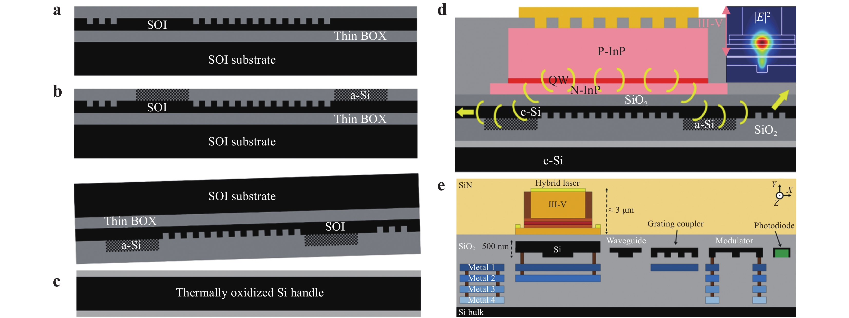
Fig. 11
We note that this new platform concept shares certain similarities with the InP membrane-on-Si (IMOS) platform172, 173, which defines all or most of the optical functionalities on a generic III-V PIC layer174 first and transfers it to a Si handle wafer or eventually a CMOS wafer full of logic/driver chips via polymer bonding172, 173. The platform is novel in many ways in comparison with conventional hybrid integration, which we defined at the beginning, particularly its vision to achieve a 3D EO integration scheme. However, considering that the III-V thin film is already partially processed on its small-scale native substrate at the point of polymer bonding, we categorise it as an innovative emerging platform in hybrid integration.
Along a similar line, micro-transfer-printing (μTP)175, 176, another extremely innovative technique for dissimilar material integration, has recently gained increasing popularity in Si photonic integration177-182. This technique essentially entails a pick-and-place process to transfer one or many micrometre-sized epitaxial material die (s) from a source wafer (e.g. III-V) to another target wafer (e.g. Si) in each printing cycle. The epitaxial material dies on the source wafer can be either finished photonic components or a material consisting of blank epitaxial ‘coupons’, both with the necessary sacrificial layer underneath. Compared with bonding multiple millimetre-sized bare III-V dies either with the same or a different epitaxial structure to a large Si wafer, μTP offers the same flexibility of device functionality enablement by transferring the best epitaxial thin films, but with much less III-V material waste for potentially reusable III-V substrates and significantly smaller III-V dies. The transferred epitaxial material dies can also be further processed in a large Si wafer. Lasers, amplifiers, and photodetectors on Si, which were obtained via μTP, and which deliver acceptable performance, have been demonstrated in quick succession in the past few years, and additional information can be found in a good review183. Prior to being picked up by the polymer stamp, however, even bare III-V coupon transfer requires a minimum of three lithography and material etching cycles to define the die size, define the sacrificial portion, and encapsulate the dies and form the tethers on the source III-V wafers, respectively183. Device fabrication on the III-V source wafer before μTP still entirely relies on the conventional small-scale III-V process. Despite full acknowledgement of the novelty and attractive merits of μTP, the technique is not included in our definition of heterogeneous integration and will not be discussed in more detail here.
Another innovative and powerful platform-level concept successfully implements III-V band gap engineering on Si by direct epitaxy rather than by wafer bonding of multiple III-V epitaxial thin films184, 185. Fig. 12 presents one of the most recent fabrication flows to embody this concept by a leading group in this field at NTT186. Firstly, the InP epitaxial thin film was transferred to a 2 μm-thick SiO2/Si substrate by molecular wafer bonding at low temperature (<350 °C) to serve as the III-V epitaxy template (Fig. 12a). Mismatches in the lattice constant, polarity, and thermal expansion of materials are known to be fundamental intertwined roadblocks for high-quality direct heteroepitaxy, for example, the growth of a III-V material with low-dislocation density directly on Si. Here, a bonded InP template is used to decouple three mismatches and eliminate lattice and polarity mismatches. The MQW active region is then grown on this heterogeneous template using blank epitaxy or selective epitaxy (Fig. 12c) if the selective growth window is defined by a patterned dielectric mask in advance (Fig. 12b). Slightly different MQW structures for different laser gain peaks can be conventionally realised in a single epitaxy step by defining dielectric mask windows with varied dimensions186. Because of the remaining thermal mismatch, epitaxy is limited to a few hundred nanometres (e.g. <430 nm) to maintain the entire III-V stack below the critical thickness to avoid dislocation generation187, 188. These thin III-V stacks on SiO2 also result in strong optical confinement to the MQW, a critical advantage to build low-threshold and high-speed lasers185, 187, 188. Furthermore, compared with the general micrometre-thick III-V stack in conventional heterogeneous devices, this thin III-V stack facilitates mode transition from III-V to either Si strip waveguides buried in the SiO2 layer underneath or SiNx waveguides on the same plane. A thin III-V stack leads to a small phase mismatch with a Si strip waveguide189, and the simplicity of forming a III-V inverse taper, that is, spot-size-converter (SCC)186. Upon the III-V mesa was formed (Fig. 12d), the second epitaxy was used to grow a layer of undoped InP for passivation of the III-V mesa, resulting in a buried heterostructure (BH) (Fig. 12e). Such a BH structure is widely used to passivate the exposed active region and achieve a small active region volume for high injection efficiency in high-performance diode lasers. The structure was first demonstrated by selective epitaxy on a wafer-bonded thick vertical p-i-n heterogeneous laser structure on an SOI substrate184. The limited thickness of the III-V stack makes it impossible to form a conventional vertical p-i-n structure, thus a lateral p-i-n structure was realised by the thermal diffusion of Zn (p doping) and ion implantation of Si (n doping) (Fig. 12f). Finally, the formation of a surface grating with large coupling strength to the lasing mode and metallization completed the fabrication of the compact DFB laser (Fig. 12g), and an SSC was defined to couple light into the on-chip SiNx or polymer waveguides (Fig. 12h). An O-band 8-channel directly modulated (25.8 Gbps/channel) membrane laser transmitter was fabricated using this flow186. A mean channel spacing of 860 GHz was the result of the detuned MQW gain peak in the first selective regrowth and a slightly different surface grating pitch for each channel.
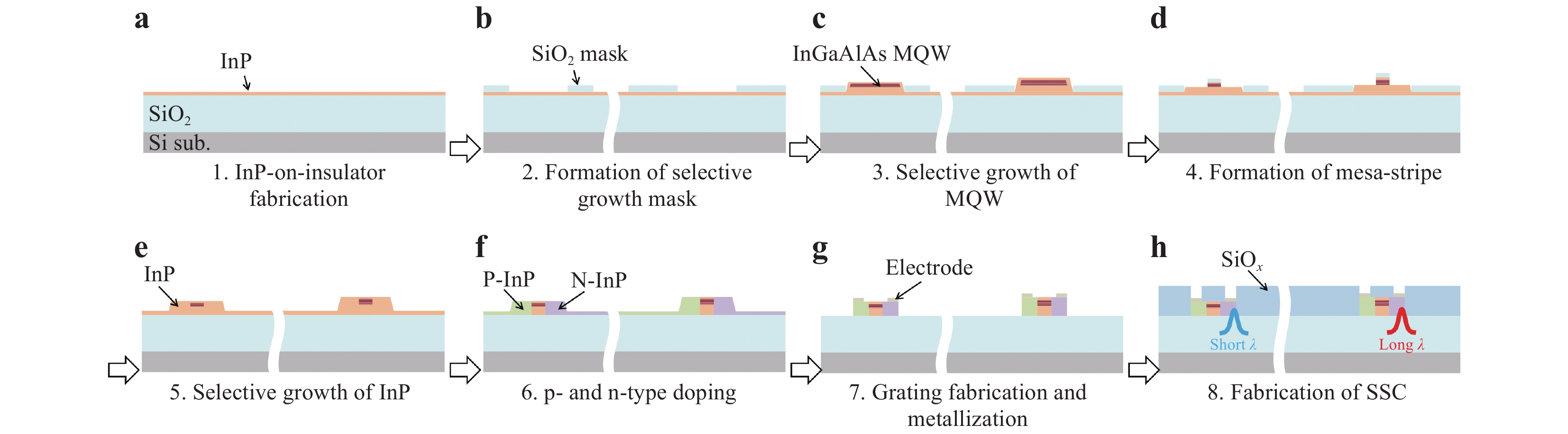
Fig. 12
Schematic of fabrication process flow for selectively grown multi-channel membrane laser array on SiO2/Si substrate186.An earlier version of such a membrane laser platform enabled the thin MQW-based laser stack to be bonded onto the SiO2/Si substrate, and required only one regrowth to form the BH structure185. The same HIC waveguide structure and lateral BH p-i-n diode laser configuration enabled extremely impressive device performance, including record-low threshold lasing on Si of 24 pA and corresponding record-high energy efficiency of 7.3 fJ/bit at 10 Gb/s NRZ direct modulation189, and 50 Gb/s direct NRZ modulation190, 191. Noteworthy is that a record-high direct laser modulation bandwidth >100 GHz resulting in record-fast signal modulation of 325 Gb/s from a single laser was demonstrated in a similar heterogeneous membrane laser192, 193. The laser was integrated on a SiC substrate instead of a SiO2/Si substrate for improved device Joule heat dissipation. A self-injection locking device scheme was employed to largely extend the intrinsic device resonance frequency. In addition to high-performance lasers186-189, 194-196, other devices that have been fabricated on this platform are competitive amplifiers197, 198, modulators198, 199, photodetectors200, 201, and PICs198, 199, all sharing compact lateral p-i-n BH structures to allow a powerful dense integration of all building blocks on the same Si chip.
Several other groups have been pursuing a similar strategy of direct epitaxy on wafer-bonded III-V templates on SOI202-204, SiO2/Si205, 206, or bulk Si substrate21. Although the thin lateral p-i-n diode structure provides favourable strong modal confinement to the active region, it is neither trivial to implement nor easy to achieve a planar surface after selective regrowth. Therefore, several studies have attempted to grow conventional thick vertical p-i-n diode structures on this bonded template. Fig. 13a shows an atomic force microscopy (AFM) image of a ~2 μm thick MQW-based diode laser structure grown on a 150 nm-thick n-InP layer bonded onto a patterned SOI substrate202, 203. A smooth surface with a roughness of ~0.2 nm RMS was measured, which is identical to that of a witness sample with an InP native substrate at the same time. The transmission electron microscopy (TEM) image in Figs. 13b-c shows a threading dislocation-free III-V cross section and well-preserved material integrity in the MQW. This was also confirmed by the strong satellite peaks in the high-resolution X-ray characterization (Fig. 12d). The low dislocation density of 9.5 × 104 cm−2 measured at the III-V surface is only one order of magnitude higher than that of the same epitaxial structure grown on native InP substrates. This indicates an interesting weak dependence of the dislocation density on an epitaxy thickness beyond the critical thickness. It also eliminates dislocation-induced device lifetime concerns for practical applications126. The diode laser performance of this structure203 as well as that of another 3 μm-thick epitaxy design were encouraging206.
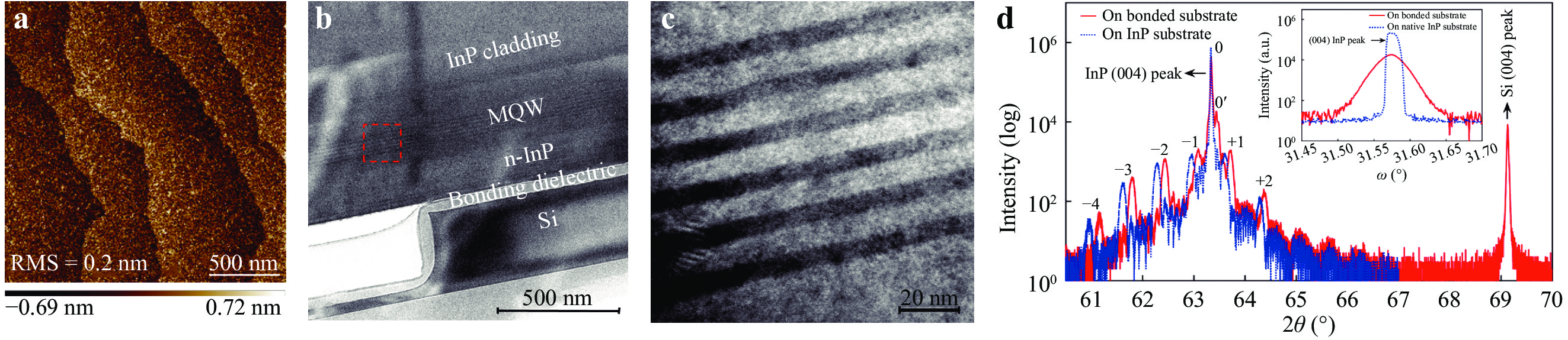
Fig. 13
Images for characterisation of the fabricated device. a AFM, b TEM, c enlargement of the area enclosed within the red square in b, and d high-resolution X-ray ω-2θ measurement of the epitaxy. Inset: high-resolution omega scans of the InP (004) peak203.This approach of using epitaxy on a bonded template transplants many attributes from conventional monolithic III-V PIC technology, for example, formation of the BH structure and flexible bandgap engineering from selective regrowth, onto large-scale heterogeneous Si substrates. Compared with rapidly progressing monolithic III-V-on-Si integration207, 208, this approach embraces seamless optical coupling between the III-V material and low-loss passive Si or SiNx waveguide, owing to the thin bonded III-V template that avoids the necessary 2-3 μm-thick III-V buffer layer growth in the monolithic approach. On the other hand, this combination platform may naturally not be considered to be cost-effective because of the involvement of wafer bonding and at least two epitaxy processes, one on the native III-V substrate and one(s) on the Si substrate. However, one may argue that the cost saving resulting from the epitaxy on a large-scale (200-300 mm) Si substrate is likely to dwarf the additional cost from the initial simple template epitaxy on a small (50-100 mm) native substrate. Selective epitaxy in photolithography-defined growth windows also leads to a larger integration density and more flexible placement of III-V active devices, in comparison with challenges to handle small dies and minimal dimension limits of several square millimetres in conventional multiple die-to-wafer bonding. Before the monolithic heteroepitaxial solution reaches maturity, this combined approach is expected to continue to grow into a larger field between pure heterogeneous and monolithic Si photonics.
Direct heteroepitaxy of high-quality functioning thin-film material on Si is widely considered to be the ultimate solution from the perspective of the production cost, yield, and throughput. For III-V-on-Si heteroepitaxy, frontline research still aims to reduce the dislocation density using a variety of means209-213. Recent attempts to grow QD gain medium on Si to leverage its enhanced defect immunity to dislocations over the QW counterpart resulted in a giant leap towards reliable monolithic light sources on Si207, 208, 214, 215. Commercial applications at elevated temperatures demand a dislocation reduction of another factor of 10 or more to the low 105/cm2 range126. Low-loss optical coupling from III-V to Si photonic circuits on the same chip represents another major obstacle before heteroepitaxial III-V materials can replicate the majority of functionalities of wafer bonded materials. However, in certain scenarios in which thin film materials (e.g. LiNbO3) and special structures (e.g. thin film-on-insulator layer stacks and III-V/oxide/Si MOS capacitors) are fundamentally not possible using a monolithic approach, bonding-enabled heterogeneous integration remains irreplaceable and is anticipated to continue to flourish in integrated photonics for a long time.
-
Approximately 15 years ago, the novel idea of attaching crystalline III-V compounds to Si with the aim of lighting up this flagship semiconductor also motivated a few groups of scientists who not only considered it to be a research topic but who believed that it would become a compelling technology to ride the datacom wave and transform the entire landscape of integrated photonics. As researchers who are fortunate enough to be deeply involved in this challenging and exciting process, we started this review by categorizing technology branches within the scope of heterogeneous Si photonic integration from our point of view. An overview of mainstream wafer bonding methods was then presented to discuss their respective strengths and weaknesses as bonding is the most critical fabrication step in heterogeneous integration. The key technical benchmarks Intel disclosed in relation to efficient, robust, and reliable lasing manifest the engineering excellence behind their commercial success.
We then reviewed three aspects of recent technical progress at the device level. 1) Application-driven spectral extension in heterogeneous lasers from 850 nm to over 4 μm was accomplished by selecting the appropriate materials for lasing at the wavelength of interest and low-loss passive waveguiding on Si. 2) Several examples of record-setting device performance include narrow-linewidth external cavity lasers with minimal Lorentzian linewidth of 140 Hz, QD comb lasers with 3 dB comb width of 12 nm, and AlGaAs-on-insulator high-Q resonators with a minimal pump power of 36 μW for frequency comb generation. They all perfectly embody the essence of heterogeneous integration by amplifying the unique material merits of each element. 3) A heterogeneous MOS capacitor as an example of fundamental element innovation that activates a forgotten aspect of the electrical properties of Si in this heterogeneous platform. Unprecedented low-energy phase tuning and inherently improved high-speed dynamics over their Si MOS counterparts make these capacitors a powerful addition to lasers, modulators, switches, filters, and so on, all of which are fabricated using an identical process to allow straightforward integration on the same heterogeneous platform.
Finally, two representative innovations at the platform level were discussed in detail. The ‘back-side’ heterogeneous platform was developed to modify the process and configuration on the Si side prior to III-V bonding. The platform was designed to complete all high-temperature processes, define all functionalities in Si and the add-on monolithic materials such as SiNx and Ge, and transfer this device function-ready layer onto another SiO2/Si handle wafer to realise a smooth planar back-side surface for convenient III-V thin film transfer. The second platform combined heterogeneous and monolithic integration in a novel fashion by successfully attempting high-quality III-V epitaxy on a thin III-V layer wafer bonded onto a Si-based substrate. The special lateral p-i-n BH structure on this platform resulted in numerous major performance records, not only the best in the class of heterogeneous lasers, but also of the entire diode laser family. Competitive amplifiers, modulators, photodetectors, and several co-integrated devices demonstrated favourable fabrication compatibility and platform versatility. Thicker vertical p-i-n III-V structures were also grown on bonded templates, and high material integrity was verified by rigorous material characterizations and decent laser device performance.
An observation from a number of examples in the literature216 is that more innovations and development around SiNxwere taking place in the past 10 years because of the much lower passive loss, medium refractive index contrast to SiO2 and air, and favourable nonlinear characteristics. In addition, SiNx is CMOS compatible, making it easy for production CMOS foundries to adopt this material.
Another recent area of major progress in heterogeneous Si photonics is lithium niobate (LiNbO3) thin-film photonics. The exceptional linear and nonlinear electro-optic effects32 and low optical loss217 of traditional bulk LiNbO3 are well preserved in the thin film format after heterogeneous integration on Si. As it is already commercially available218, thin film LiNbO3 is highly attractive for >100 Gbaud/s applications219 and frequency comb generation220. Similarly, additional compounds with special properties, such as barium titanate, are being explored to provide materials with strong electro-optic effects from which crystalline Si is missing221, 222. However, they are beyond the scope of this review.
Heterogeneous Si photonics has since become a vast field, intertwined by more materials, improved fabrication processes, and deep multi-physics, and records are being rewritten so often that no one can confidently capture all recent shining points in one review paper. Many excellent reviews71, 187, 223-226 on the latest progress have inspired us as they have done to many others. In the foreseeable future, Si as a firmly established flagship material is expected to continue to be the dominant substrate for heterogeneous photonic integration. Wafer bonding is a generic integration technique that helps the Si substrate to accommodate more functioning thin film materials. Therefore, research breakthroughs resulting from the heterogeneous integration of materials, fabrication methods, or physics are anticipated to continue thriving at an accelerating and exciting pace. In terms of commercial product development, certain niche applications that are less cost sensitive, for example, space, defence, and metrology, are likely to welcome the heterogeneous integration of multiple different thin films even from different families of materials for the best possible performance of the target. However, this would be subject to more complicated fabrication procedures and smaller yields. Volume applications such as transceivers in data centres, 5G networks, and Lidar in automobiles would benefit from the lower cost resulting from economies of scale. Therefore, keeping changes in the mature CMOS process to the minimum to retain only the functionality that absolutely requires heterogeneous integration would favour shorter process development, a shorter production cycle, and higher yield. In summary, trade-offs between functionality/integration density and fabrication compatibility/complexity/volume can be expected to continue to guide the industry to make rational decisions in the best interest of each application.
-
The authors acknowledge generous support from US government agencies, academic and industrial collaborators, colleagues, students and families throughout the years to enable our continuous research in this field. The authors also acknowledge Dr. Robert Herrick, Dr. Richard Jones, Dr. Hyundai Park, Dr. Lin Chang, Dr. Takuro Fujii and Dr. Shinji Matsuo for useful discussion, granting copyright and sharing the high-resolution images of their work.

 DownLoad: