2021 Vol. 2, No. 1
Published. 2021, 2(1)
: 9-19
doi: 10.37188/lam.2021.001
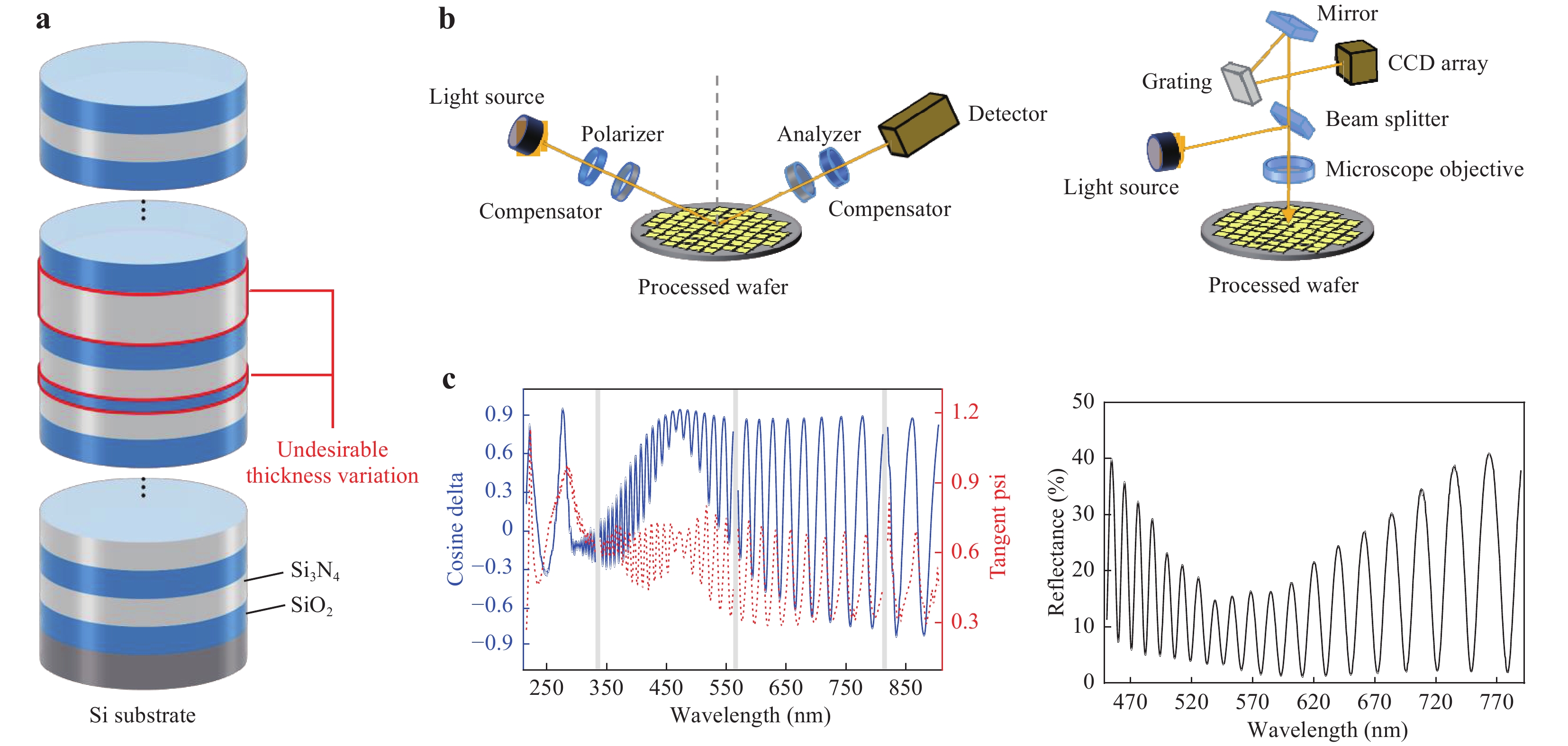
Three-dimensional (3D) semiconductor devices can address the limitations of traditional two-dimensional (2D) devices by expanding the integration space in the vertical direction. A 3D NOT-AND (NAND) flash memory device is presently the most commercially successful 3D semiconductor device. It vertically stacks more than 100 semiconductor material layers to provide more storage capacity and better energy efficiency than 2D NAND flash memory devices. In the manufacturing of 3D NAND, accurate characterisation of layer-by-layer thickness is critical to prevent the production of defective devices due to non-uniformly deposited layers. To date, electron microscopes have been used in production facilities to characterise multilayer semiconductor devices by imaging cross-sections of samples. However, this approach is not suitable for total inspection because of the wafer-cutting procedure. Here, we propose a non-destructive method for thickness characterisation of multilayer semiconductor devices using optical spectral measurements and machine learning. For > 200-layer oxide/nitride multilayer stacks, we show that each layer thickness can be non-destructively determined with an average of approximately 1.6 Å root-mean-square error. We also develop outlier detection models that can correctly classify normal and outlier devices. This is an important step towards the total inspection of ultra-high-density 3D NAND flash memory devices. It is expected to have a significant impact on the manufacturing of various multilayer and 3D devices.
Published. 2021, 2(1)
: 20-30
doi: 10.37188/lam.2021.002
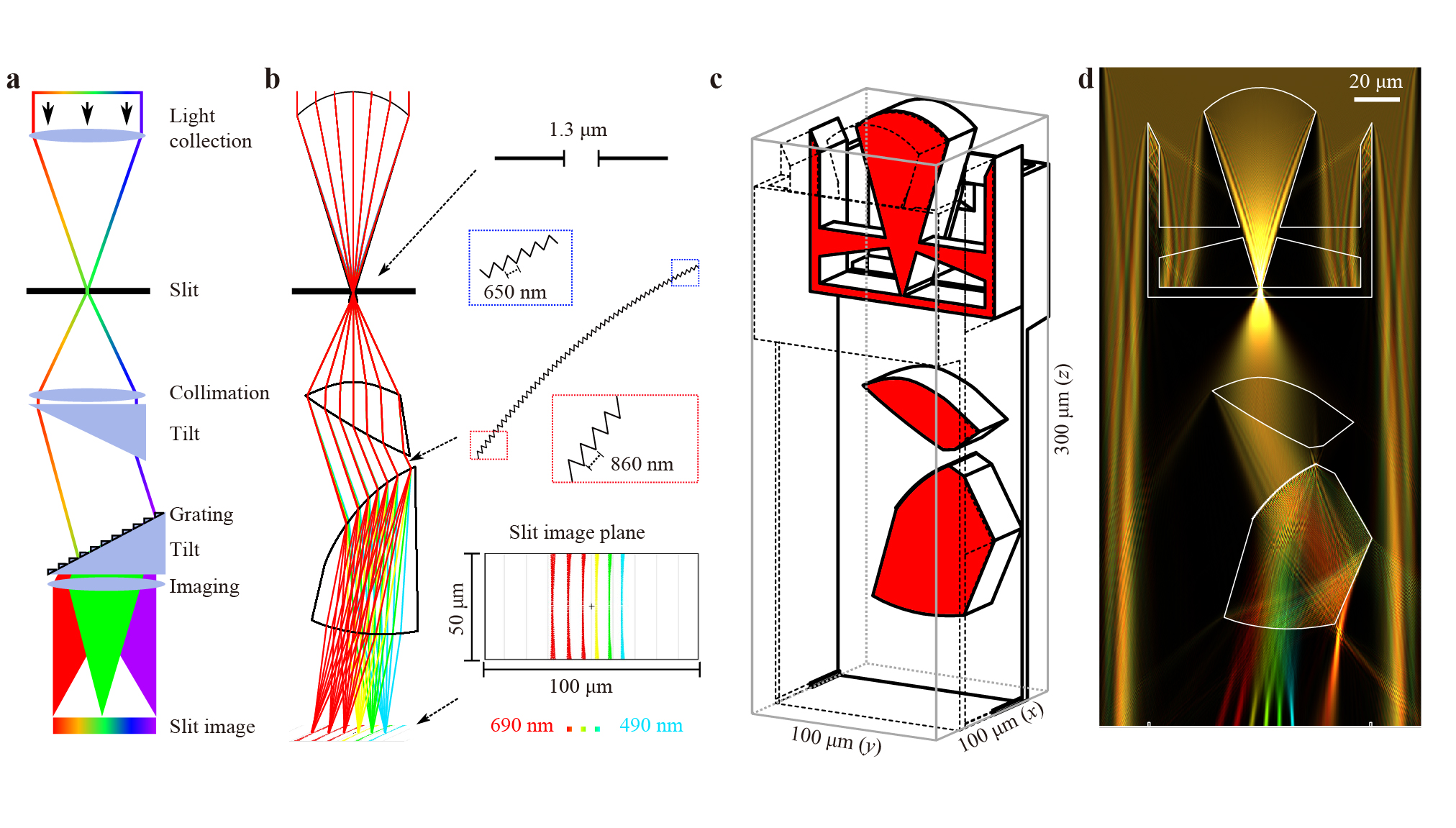
The miniaturisation of spectroscopic measurement devices opens novel information channels for size critical applications such as endoscopy or consumer electronics. Computational spectrometers in the micrometre size range have been demonstrated, however, these are calibration sensitive and based on complex reconstruction algorithms. Herein we present an angle-insensitive 3D-printed miniature spectrometer with a direct separated spatial-spectral response. The spectrometer was fabricated via two-photon direct laser writing combined with a super-fine inkjet process. It has a volume of less than 100 × 100 × 300 μm3. Its tailored and chirped high-frequency grating enables strongly dispersive behaviour. The miniature spectrometer features a wavelength range of 200 nm in the visible range from 490 nm to 690 nm. It has a spectral resolution of 9.2 ± 1.1 nm at 532 nm and 17.8 ± 1.7 nm at a wavelength of 633 nm. Printing this spectrometer directly onto camera sensors is feasible and can be replicated for use as a macro-pixel of a snapshot hyperspectral camera.
Published. 2021, 2(1)
: 31-38
doi: 10.37188/lam.2021.003
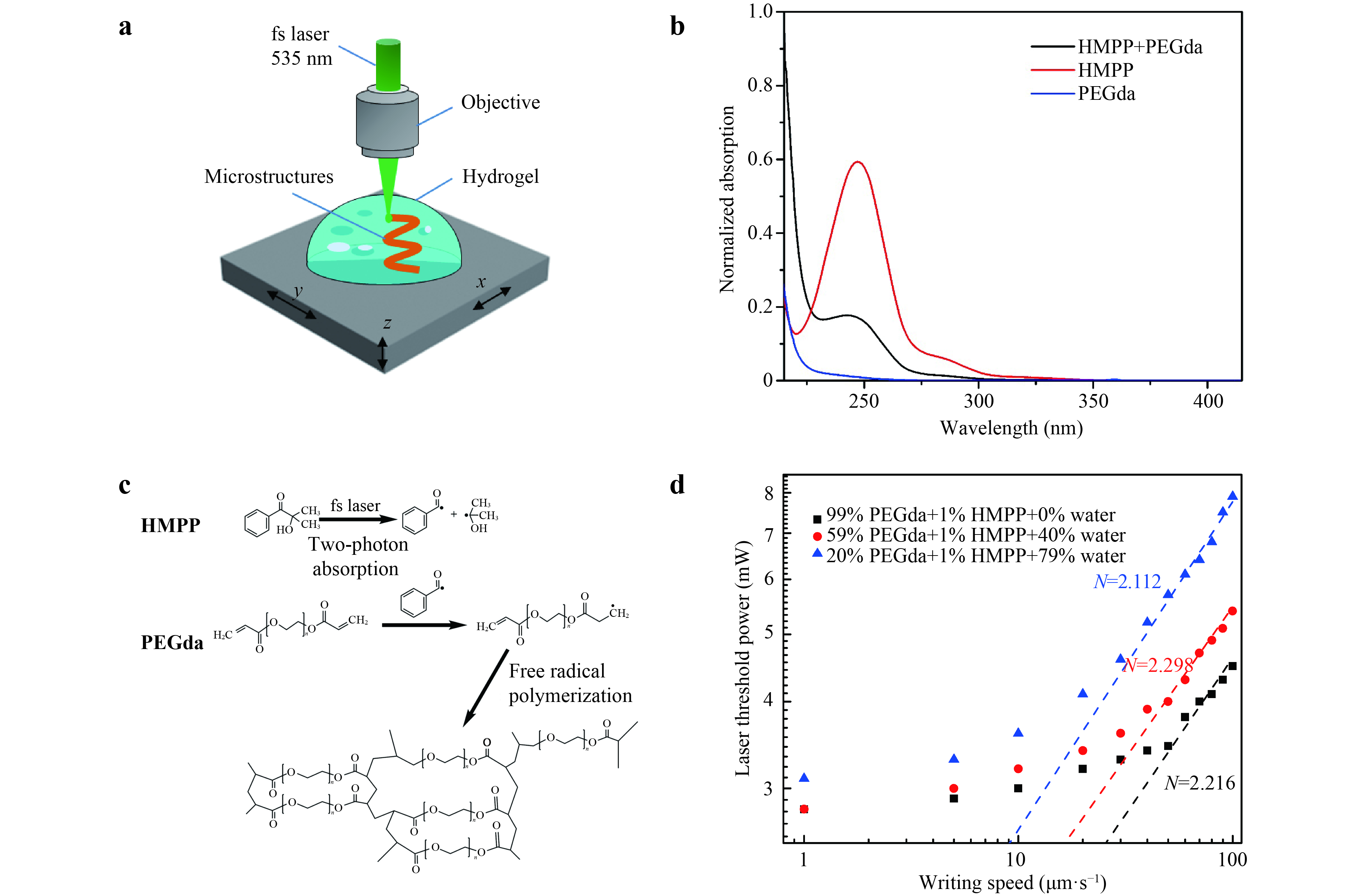
Three-dimensional (3D) direct laser writing (DLW) based on two-photon polymerisation (TPP) is an advanced technology for fabricating precise 3D hydrogel micro- and nanostructures for applications in biomedical engineering. Particularly, the use of visible lasers for the 3D DLW of hydrogels is advantageous because it enables high fabrication resolution and promotes wound healing. Polyethylene glycol diacrylate (PEGda) has been widely used in TPP fabrication owing to its high biocompatibility. However, the high laser power required in the 3D DLW of PEGda microstructures using a visible laser in a high-water-content environment limits its applications to only those below the biological laser power safety level. In this study, a formula for a TPP hydrogel based on 2-hydroxy-2-methylpropiophenone (HMPP) and PEGda was developed for the fabrication of 3D DLW microstructures at a low threshold power (0.1 nJ per laser pulse at a writing speed of 10 μm·s−1) in a high-water-content environment (up to 79%) using a green laser beam (535 nm). This formula enables the fabrication of microstructures with micrometre fabrication resolution and high mechanical strength (megapascal level) and is suitable for the fabrication of water-responsive, shape-changing microstructures. These results will promote the utilisation of low-power 3D DLW for fabricating hydrogel microstructures using visible lasers in high-water-content environments.
Published. 2021, 2(1)
: 39-58
doi: 10.37188/lam.2021.004
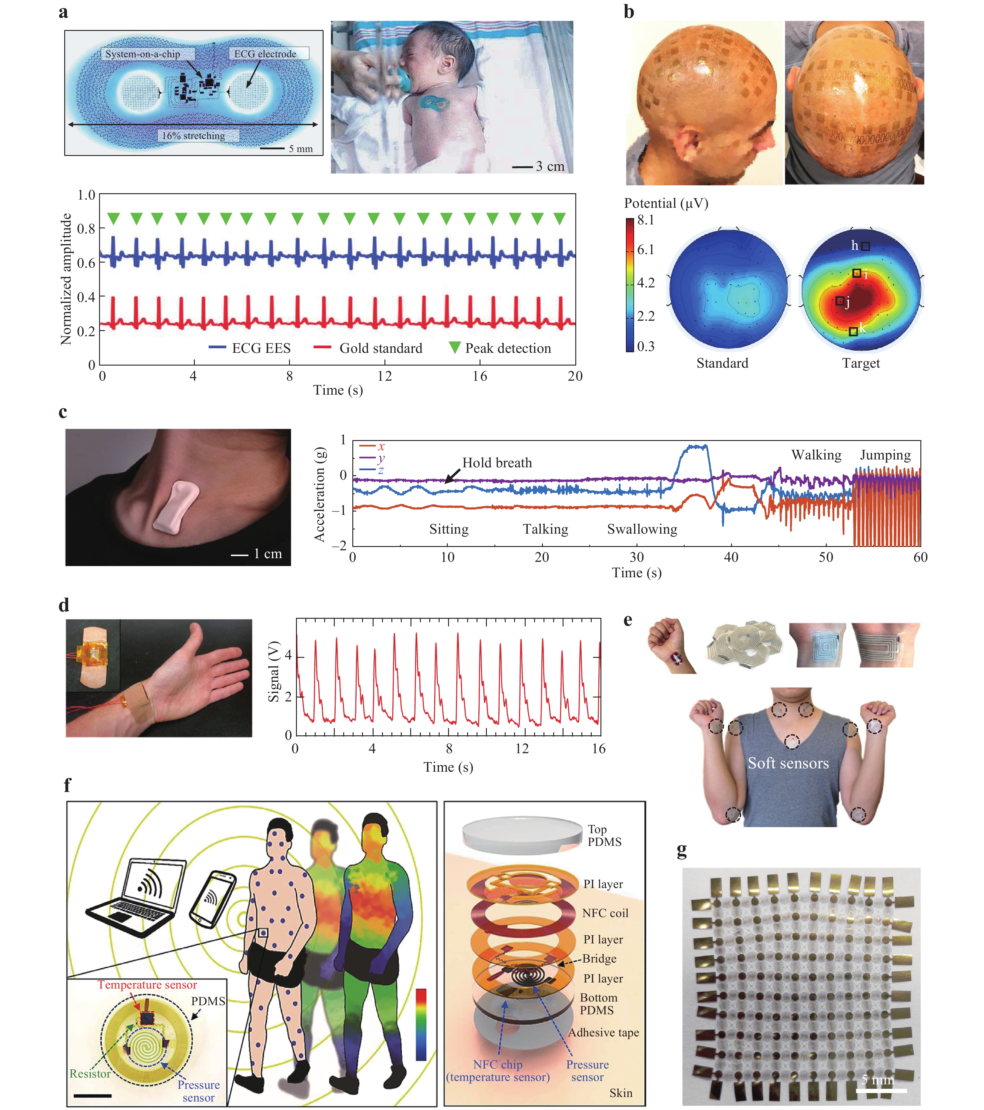
Skin-integrated electronics are a novel type of wearable devices that are mounted on the skin for physiological signal sensing and healthcare monitoring. Their thin, soft, and excellent mechanical properties (stretching, bending, and twisting) allow non-irritating and conformal lamination on the human skin for multifunctional intelligent sensing in real time. In this review, we summarise the recent progress in the intelligent functions of skin-integrated electronics, including physiological sensing, sensory perception, as well as virtual and augmented reality (VR/AR). The detailed applications of these electronics include monitoring physical- and chemical-related health signals, detecting body motions, and serving as the artificial sensory components for visual-, auditory-, and tactile-based sensations. These skin-integrated systems contribute to the development of next-generation e-eyes, e-ears, and e-skin, with a particular focus on materials and structural designs. Research in multidisciplinary materials science, electrical engineering, mechanics, and biomedical engineering will lay a foundation for future improvement in this field of study.
Published. 2021, 2(1)
: 59-83
doi: 10.37188/lam.2021.005
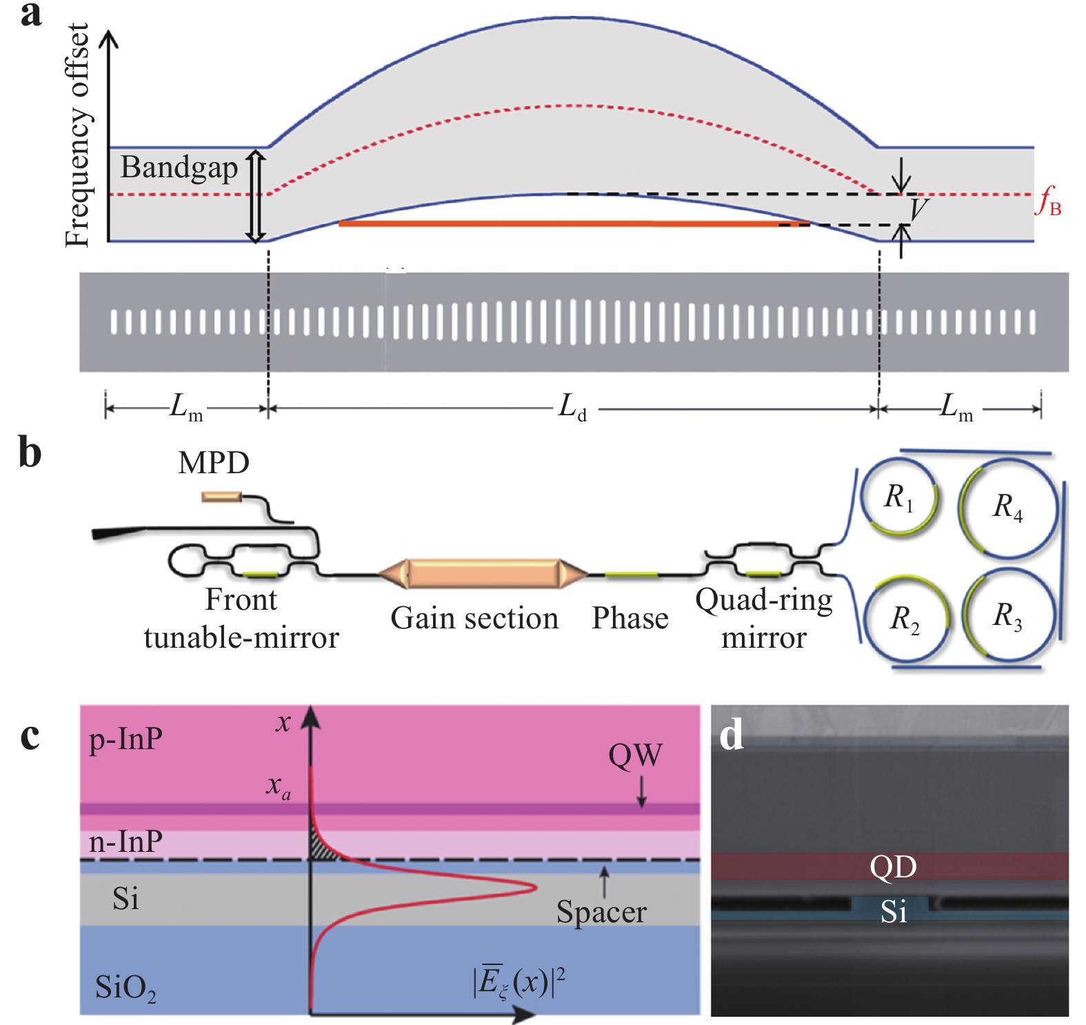
Silicon (Si) photonics is a disruptive technology on the fast track to revolutionise integrated photonics. An indispensable branch thereof, heterogeneous Si integration, has also evolved from a science project 15 years ago to a growing business and compelling research field today. We focus on the scope of III-V compound semiconductors heterogeneously integrated on Si substrates. The commercial success of massively produced integrated optical transceivers based on first-generation innovation is discussed. Then, we review a number of technological breakthroughs at the component and platform levels. In addition to the numerous new device performance records, our emphasis is on the rationale behind and the design principles underlying specific examples of materials and device integration. Finally, we offer perspectives on development trends catering to the increasing demand in many existing and emerging applications.
Published. 2021, 2(1)
: 84-100
doi: 10.37188/lam.2021.007
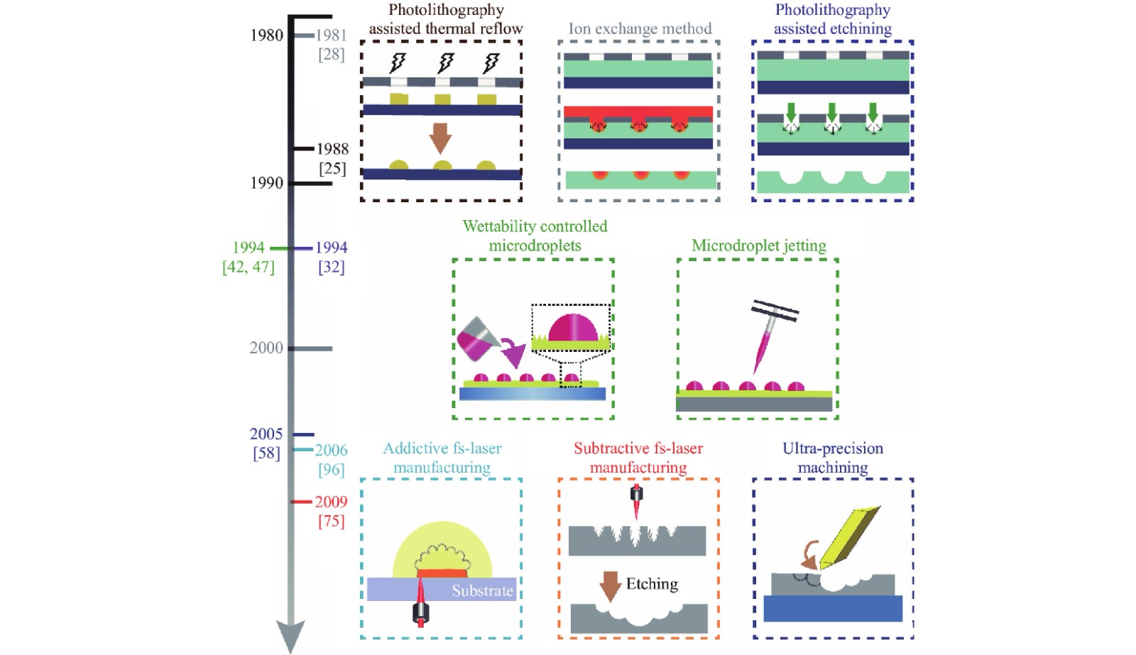
Compound eyes (CEs) are advanced optical visual systems with distinct features of large view-fields, infinite depth of field, and dynamic imaging capability, revealing their significant potential in applications including robot vision, unmanned aerial vehicle detection, and medical diagnosis. Compared with macroscopic CEs, which primarily comprise multicamera arrays, compact integrated CEs have garnered significant attention because of their portability and possibility of flexible integration with microrobots and in-vivo medical facilities. To date, considerable effort has been devoted to this field, in which manufacturing technologies are vital to the development of artificial CEs (ACEs) capable of large field-of-view imaging, depth information collection, and three-dimensional imaging. Challenges and opportunities exist for the practical application of advanced ACEs. This paper reviews state-of-the-art technologies for manufacturing ACEs, and then briefly summarises their potential applications in different fields. Finally, the current challenges and perspectives of ACEs are discussed.



 Email
Email RSS
RSS