


-
Quality demands on mechanical and electrical components are increasing steadily, especially for mass-produced parts, for example, in the automotive industry, medical technology, and chip production and assembly in the semiconductor industry. On the one hand, tighter tolerances require very precise measuring methods; on the other hand, the demand for full-field inspection of functional surfaces on 100% of all parts is increasing, and these requirements conflict. Tactile measuring systems are still very common and, in many cases, meet the requirements for accuracy. However, owing to the pointwise tactile recording, a complete surface measurement is, in most cases, not reasonable or possible. Hence, the use of coordinate measurement systems is almost exclusively limited to the inspection of samples in special measurement rooms. Contactless optical measurement methods can overcome these limitations. In optical metrology, a distinction must be made between pointwise and full-field measuring methods. Although optical scanning can be performed orders of magnitude more quickly than tactile measurement, camera-based full-field recording methods have clear advantages in terms of overall acquisition time.
When choosing an optical sensor for a specific application, the question of whether a surface to be measured is suitable for optical inspection is very important. Reflectivity, transmission, scattering, absorption, and slope angle have a strong influence on the signal strength and thus the measurement result. Typically, reflective and matt surfaces can be distinguished. In the case of reflective surfaces, the phase front of the illumination is significantly influenced only by the shape of the specimen. Matt surfaces, on the other hand, usually destroy the phase relationship through scattering and multiple reflections, a phenomenon which is observable as a speckle effect under coherent lighting.
A large number of previously unresolved measuring tasks have the following similarities:
• Surface reflectivity is often on the edge between reflective and matt or varies rapidly over the surface. Hence, the reflective and matt regions must be measured simultaneously.
• The object’s slope has partly steep edges. Owing to the small tolerances, the absolute measurement accuracy must be less than a single micron (three sigma); in some extremely demanding applications, the requisite accuracy is down to the range of 0.1 microns. Fast production cycles and necessary time for part handling often provide no more than 0.1 seconds for measurement, especially in automotive and semiconductor series production.
Nearly every optical 3D sensor based on active illumination can be classified into one of the following five classes: (1) triangulation, (2) coherence scanning interferometry, (3) laser scanning confocal microscopy, (4) reflectometry, and (5) interferometry. To understand the limitations of each class, it is necessary to identify the dominant noise source and the influence of surface properties. Triangulation techniques cannot fulfil the abovementioned accuracy requirements owing to speckle noise and vanishing signals in reflecting regions. Additionally, steep edges are partly shadowed depending on the direction of illumination and imaging, as well as the triangulation angle. Coherence scanning interferometry and laser scanning confocal microscopy are, in principle, capable of measuring reflecting and matt surfaces, but require recording a large number of images, depending on the intended accuracy. Therefore, in both cases, fast measurements of large fields of view are limited by the depth sampling and measurement range. Reflectometry only works on fully mirroring surfaces. In principle, classical interferometry in combination with phase-shifting techniques has the potential to fulfil the requirements for accuracy and measurement time. Depending on the applied phase-shifting technique, only one image (spatial phase shifting) or a handful of images (temporal phase shifting) per field of view need to be captured1.
Based on three temporal phase-shifted images per wavelength, the number of raw image data points to be taken is at least one order of magnitude smaller than for all methods with comparable accuracy, such as coherence scanning interferometry or laser scanning confocal microscopy2.
One major limitation of classical interferometry is the restricted unambiguity range of half of the wavelength of the illuminating laser light, which means that only surfaces of optical quality can be measured suitably. Multiple wavelengths can be used to circumvent this limitation. By subtracting the phase maps generated by different wavelengths modulo 2π, a phase map at the beat frequency of the respective wavelengths can be calculated. Several of these artificial (or “synthetic”) wavelengths can be generated by recording interferograms at various wavelengths. Subsequently, the reconstructed phase maps can be cascaded such that the smaller synthetic wavelengths compensate for the phase noise of the larger ones. Therefore, the largest synthetic wavelength restricts the unambiguity measurement range, while the smallest one limits the measurement accuracy3, 4. In the case of mirror-like surfaces, the smallest wavelength can be one of the single laser wavelengths used for recording5. In classic interferometry, absolute phase measurements of speckle fields generated by rough surfaces are not possible because the phase values are statistically distributed. By subtracting the phase maps of the correlated speckle fields recorded with an identical optical setup at two slightly shifted wavelengths, this fixed-pattern phase component is eliminated completely as long as the generated synthetic wavelengths are large compared to the roughness of the inspected surface. As a result, the numerically reconstructed phase map shows very little residual speckle noise4, 6.
Extending classical interferometry, digital holography offers another very useful property: the possibility of numerically propagating the reconstructed wavefront. This enables numerical refocusing of the object plane, which has enormous advantages for inline applications. It is well known that precise sample handling in production environments to achieve the best focus position always has its limits (and costs). The application of autofocus techniques on numerically propagated wavefronts, either on amplitude or phase maps, is possible in real time7.
The content of the following sections provides a short introduction to the theoretical background of multi-wavelength digital holography and a description of the basic design of the HoloTop sensor family. The core of this publication, however, is three state-of-the-art application examples from real-world manufacturing.
We start with the first-ever published inline integration of a sensor based on multi-wavelength digital holography. The results of long-term measurements under rough production conditions on 10 million precision turned parts for the automotive industry are presented.
The demonstration of measurements on machined aluminium surfaces using a milling machine itself as a sensor mount and positioning device pushes the limits even further.
Finally, one of the most challenging applications of digital holography − the quality control of microscopic electronic interconnectors − is shown. The latest camera technology is integrated into the sensor design to fulfil the conflicting requirements of field of view, lateral sampling, and speed. The requirements for electronic device inspection are aggravated by the production cycle times of such devices (within the range of a second), sub-micron repeatability demands, and the high dynamic range of the reflecting surfaces. The most promising measurement results for microbump structures are shown.
To our knowledge, there is no alternative to digital holography for all three use cases that satisfies the simultaneous needs for accuracy, measurement field size, lateral sampling, and measurement time.
-
The term holography is derived from the Greek word holos, “whole”, and gráphein, “writing”.
In 1948, Dennis Gábor published his work in the field of minimising aberrations in electron microscopy, for which he was awarded the Nobel Prize in Physics in 1971. Holography was developed as a lensless image method for the reconstruction of complete wavefronts, that is, both amplitude and phase8.
In digital holography (DH), holographic information is not optically reconstructed but is discretely recorded using semiconductor elements such as cameras9. The amplitude and phase of waves reflected by a scattering object contain information about the topography of the illuminated object.
Previously, hologram calculations took several minutes, which initially limited the technology’s possibilities to laboratory applications. Only with increasing computing power and the availability of fast, high-resolution cameras, as well as the use of graphics processing units (GPUs), have the requirements for accuracy and production speed of today's production cycles been met; thus, DH has become increasingly relevant for industrial applications10, 11.
During hologram reconstruction, phase-shifting methods are used to convert the nonlinear intensity modulation of the recorded interferograms into relative phase values. In this context, a distinction is made between the two methods of temporal12–14 and spatial15, 16 phase shifting. Because only systems based on temporal phase shifting are presented in this paper, we refer to the literature for a comparison of both approaches17.
In holographic measurements, the height information of an object is obtained from the phase of the object wave. When measuring optically rough object surfaces, information about the macroscopic shape of an object is superimposed by an unknown speckle field. However, owing to the spatial coherence of speckle fields of different wavelengths, the macroscopic shape of an object can be extracted by a differential of the phase maps. If holograms of different wavelengths are recorded subsequently, this is referred to as temporal heterodyning3, 4.
In the past, Fraunhofer IPM has developed various digital holographic measurement systems adapted to specific applications. In the following, the architecture and structure of three of these sensors are presented. A detailed description of the workflow used for data acquisition and evaluation can be found in Ref. 4.
-
Fig. 1 illustrates the general setup of a complete multi-wavelength digital holographic measurement system. It consists of a passive sensor head (A) and a multi-laser control electronics system (B). Variations between the different systems in this contribution are marked with an asterisk.
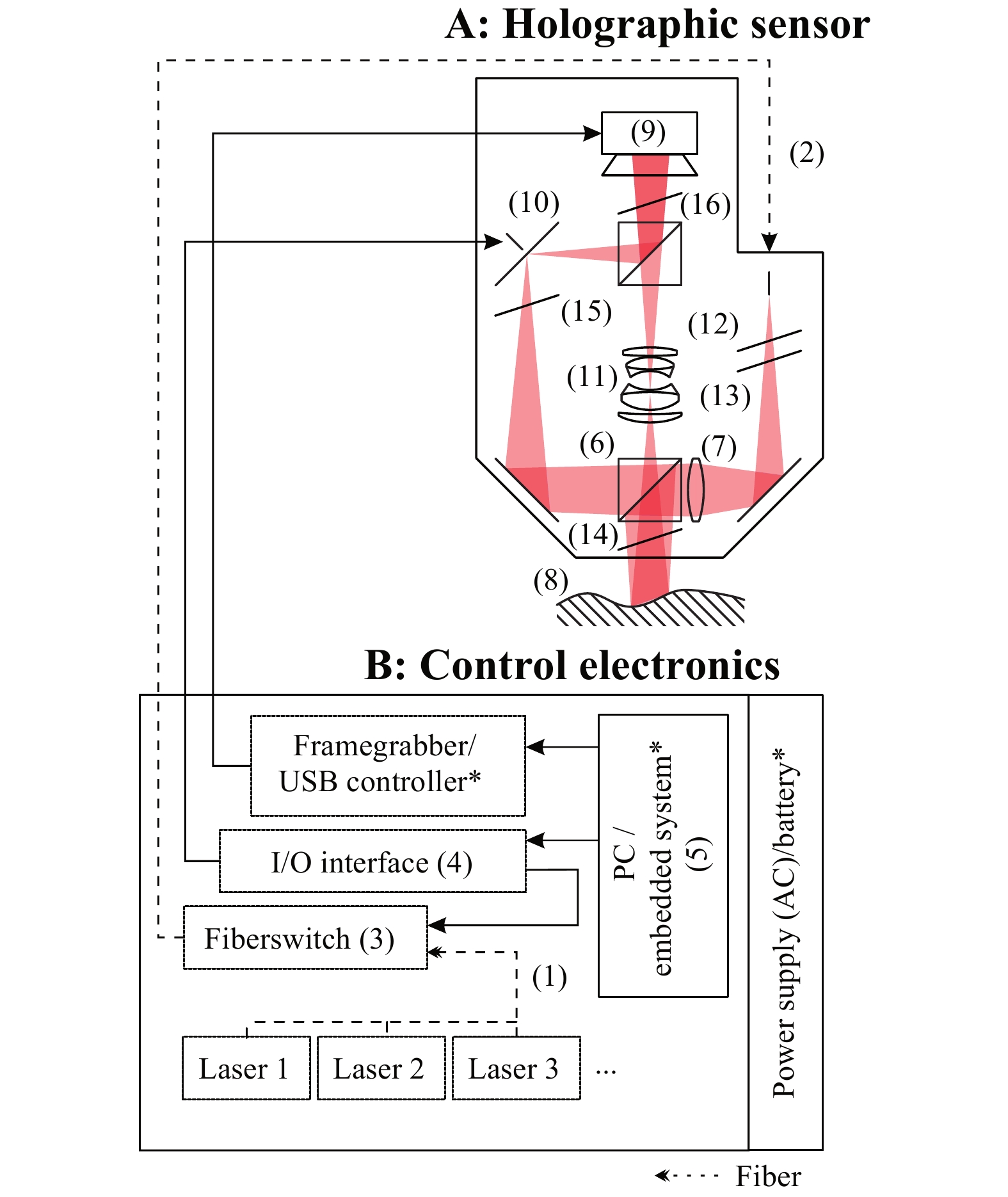
Fig. 1 Sketch of the holographic setup.
Multiple laser sources (1) are cycled through by a fiber switch (3), controlled by a computer, inside the control electronics B. Single-frequency laser light is connected to the computer-controlled (5) temporally phase shifting measurement head A by a polarization maintaining fiber (2).Multiple stabilised lasers (1) (three lasers are shown as examples in Fig. 1) with free-space optical powers of 25–50 mW are used to generate synthetic wavelengths ranging from ~2 µm to 2000 µm. For good interference contrast, the lasers must operate with a single frequency and a single mode. The laser sources (up to eight lasers) are successively coupled into the sensor head using a polarization-maintaining single-mode glass fibre (2) and switched between by a fast micromechanical fibre switch (3). The switch is controlled by an I/O interface (4) which in turn is driven by a PC or embedded system (5) inside the control electronics (B). The switching duration is specified as less than 7 ms.
Inside the sensor head (A), the beam is divided into an object and a reference beam by a polarising beam splitter cube (PBS) (6). One common lens refracts (7) the beams in such a way that they fit the size of the object (8) and the camera chip (9), respectively.
The reference beam is deflected by a mirror mounted on a piezoelectric actuator (10), which is again controlled by the I/O interface of (B). Thus, the phase of the reference beam can be shifted selectively within a single laser wavelength, which is called temporal phase shifting12.
The light scattered by the sample is imaged onto a camera sensor by an objective lens (11), where it is superimposed with the reference beam. At least three phase-shifted interferograms are recorded for each wavelength. In addition, the following polarising optics are used: a polarising filter (12) is used to minimise the influence of laser polarisation fluctuations. The beam ratio between the object and reference beams is set by a half-wave plate (13). The quarter-wave plate (14) and half-wave plate (15) are required for the beams to pass or be deflected at the following PBS. The final polarising filter (16) enables interference between the object and reference beams.
During sensor development, the measurement field and lateral resolution can be adapted to the measuring task by selecting imaging optics and a camera chip. The following example specifications given in the text refer to the HoloTop 65M sensor unless stated otherwise.
A total of nine images (three lasers used for the measurements presented in this paper, three phase steps) at a resolution of 9344 × 7000 pixels were captured within 200 ms and digitised with 10-bit resolution. The acquisition time for a three-laser configuration is determined by the following: nine images must be recorded by the camera, which is capable of a framerate of 71 frames per second; a fibre switch (Leoni 8 × 2-pm-fiberswitch) must perform two switching operations taking 10 ms each; and between each of the images, the piezo-actuator must be moved for temporal phase shifting, which takes less than 1 ms. The resulting acquisition time is thus 156 ms. A USB controller or framegrabber handles the data being transferred to the computer unit.
Using a parallelised numerical reconstruction on the GPU of the control electronics (a PC or, if available, the internal embedded system) and its Compute Unified Device Architecture (CUDA), the complete reconstruction of the phase maps at the different synthetic wavelengths, along with the evaluation of the height map, takes only 100–300 ms, depending on the filter settings. For very large camera images (65 MP) and filter radii (e.g. 7 × 7 pixels), these processes can take up to 800 ms.
This is done in two steps: first, the complex wavefront in the hologram plane is calculated using a method introduced by Cai et al.12 that compensates for vibrations and thus changes in the phase between the object and reference beam during data acquisition. Then, the complex wavefront is propagated to the focal plane without reconstruction of the disturbing twin image and zero diffraction order4, 18. A flowchart of the algorithms used for hologram reconstruction can be found in Ref. 19.
Image acquisition, data evaluation, and feature extraction are done in parallel to meet the requirements of the respective production cycle. For a detailed description and mathematics of the numerical reconstruction procedure of digital multi-wavelength holograms, we refer to3, 4, 12, 20.
All sensor heads were simulated during development using the finite element method (FEM) to ensure maximum stiffness and thus natural frequencies below externally occurring excitations. For example, a natural frequency of 605 Hz was realised using the HoloTop 20M21. This is especially important for the HoloPort system working in the machine tool. With excitation frequencies typically well below 300 Hz, the influence of external stimulations could be minimised by mechanical means at a first natural frequency of 323 Hz22.
Table 1 shows the specifications of the three holographic measurement systems developed at Fraunhofer IPM, which are presented with an application in this paper. They differ in terms of sampling and optical resolution, depending on the application they were designed for. One remarkable design consideration in the development of holographic sensors is the fact that speckle patterns generated by rough object surfaces must be sampled well, and slight oversampling yields the best results.
HoloTop 9M HoloTop 65M HoloPort Diffraction limited resolution/µm 13.5 6.4 16.2 Lateral sampling/µm 5.86 1.91 < 7 Magnification −0.94 −1.67 −0.5 Numerical aperture 0.06 0.10 0.04 Camera Sensor CMOSIS CMV12000 GPixel GMAX3265 Sony IMX253 Number of pixels 3072 × 3072 9344 × 7000 4112 × 3008 Single FOV/mm2 18.0 × 18.0 17.8 × 13.4 20 × 20 Acquisition time per point/s 6.4e-6 3e-9 3.3e-8 Acquisition time per FOV/ms ~ 100 ~500 < 500 Table 1. Specifications of selected holographic measuring systems developed at Fraunhofer IPM.
In addition to the systems presented here, there are other systems available as well: systems with a postcard-sized field of view, for measurements on moving objects, and with a microscope objective for particularly high lateral resolution23.
In a slightly modified form, the setups can also be used for deformation measurements using electronic speckle interferometry (ESPI)24, 25.
-
For every 3D sensor, the traceability of the measured height values to standards is highly important. For this purpose, we measured the step height of a calibrated height normal. The height normal consisted of two gauge blocks manufactured by Kolb & Baumann GmbH & Co. KG, which nominally differed in height by 20 µm. The real step height was measured by the National Metrology Institute of Germany PTB to be 20.138 µm with an accuracy of 0.013 µm within a temperature range of 19.85 °C to 20.00 °C. We measured the step height using a HoloTop 65M system 25 times.
The laser sources used for these measurements were three fibre coupled frequency doubled solid state lasers with a free space power output of 50 mW each (Cobolt Samba at 532.20 nm and Cobolt Fandango at 517.67 nm and 514.46 nm). The synthetic wavelengths used for measurement here were thus 82.9 µm, 15.5 µm and 15.4 µm.
A height map after the numerical removal of sample tilts is shown in Fig. 2a, and the cross-sections of the height map are shown in Fig. 2b. The height map displays height values from −5 µm (black) to +25 µm (white). Data points with insufficient data quality due to low interference contrast are shown in blue. The cross-sections for all 25 measurements in Fig. 2b are nearly identical despite a low number of single point outliers at the very steep edge of the step resulting in undersampling of fringes in the synthetic phase maps. Calculating the differences between the mean height values on the left and right parts of the height map yielded the measured step height values which are shown in Fig. 2c. The mean value of the measured height was 20.135 µm, and the standard deviation of the measured heights was calculated to be 0.010 µm. Thus, the measured height values were in excellent agreement with the reference measurements by PTB.
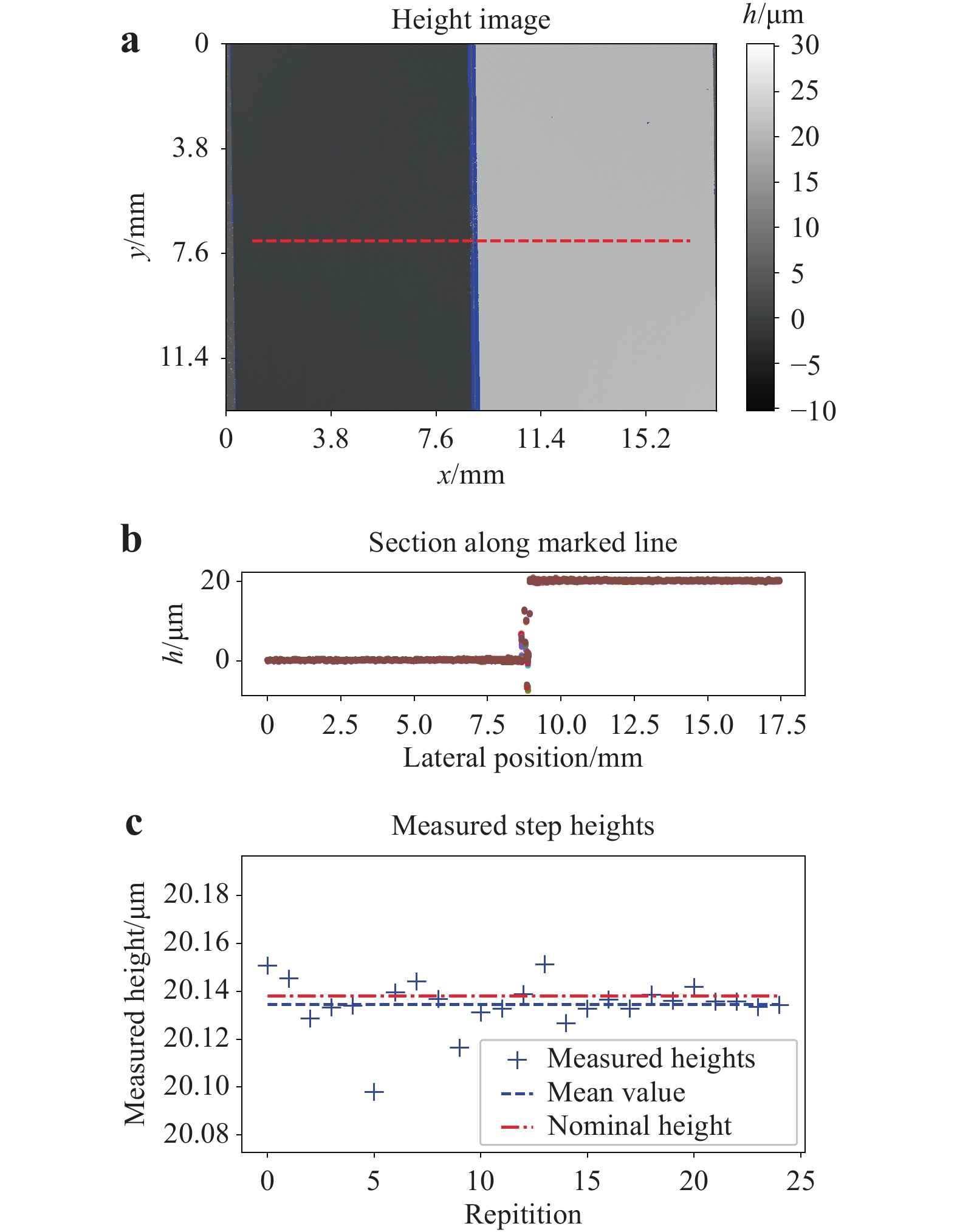
Fig. 2 Measurement results on a calibrated step height standard.
a Grey value representation of the measured height map consisting of 9344 × 7000 pixels. b Cross-section of a along dashed line. c Measured values of step height for 25 repetitions.For high-precision 3D measurements, it is very important to yield equal data quality throughout the field of view. This can be evaluated using a test target with a clearly detectable structure to ensure that the height difference can be calculated between identical regions, even if the sample is moved. The measurement data for one such sample manufactured by VLSI Standards Inc. is shown in Fig. 3. The test target consisted of a quartz substrate with a chromium cover. The grooves of the test target had a depth of 19.320 µm. The uncertainty of the groove depths was given by the manufacturer as +/−0.116 µm. It should be noted that to evaluate the homogeneity of data quality, an extremely tight uncertainty of the reference measurement is not needed because the main focus lies in the reproducibility of the holographic setup; furthermore, its absolute accuracy has been proven with the previous measurement, as shown in Fig. 2. The groove depth of the target was measured 14 times. Between each measurement, the sample was moved arbitrarily within the field of view. Fig. 3a−c show some of these measurements. The depth of the groove was calculated as the difference between the mean value measured in two regions on the top of the groove target, marked with green rectangles, and the mean value of a region inside the groove, marked with a red rectangle in Fig. 3. The dimensions of the regions on the top surface were set to 600 × 400 pixels, and those of the region inside the groove were set to 600 × 450 pixels. The results of this evaluation are shown in Fig. 3d. Each point refers to the groove depth measured at one of the fourteen different target positions. The mean value of the measured groove depths was 19.345 µm, and the standard deviation of all measured groove depths was 0.010 µm.
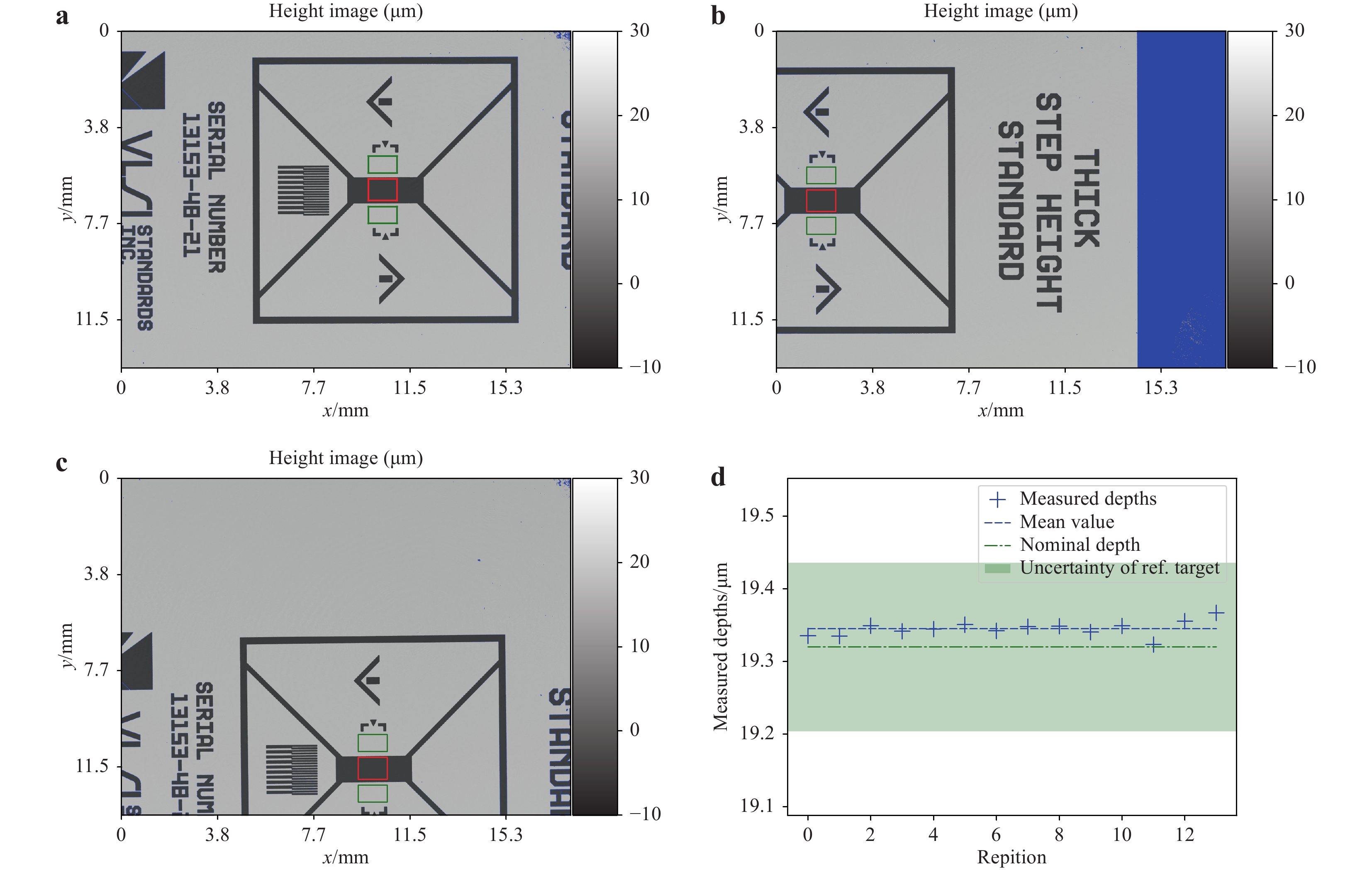
Fig. 3 Measurement results on a groove sample at different positions within the field of view.
a–c height maps for three arbitrary positions of the sample consisting of 9344 × 7000 pixels each. The regions of interest for measurement of the groove depth are marked with red and green frames. d Measured height values for 14 arbitrary positions within the field of view of the sensor compared to the reference value from calibration data and uncertainty of reference measurement as given by the manufacturer of the sample.Thus, the measured groove depths were in excellent agreement with the reference data and showed no recognisable variation across the field of view of the sensor.
-
One of the most prominent industrial applications of multi-wavelength digital holography is the inspection of high-precision sealing surfaces. These components are made from metal and produced with very tight tolerances of 10 µm and below. One manufacturer of such sealing devices for diesel injectors is Werner Gießler GmbH. This company produces approximately 10 million parts per year. Since 2015, they have been using a HoloTop 9M sensor for 100% end-of-line inspection, which means that each part produced is inspected with a digital holographic sensor21, 26. A photograph of the integrated sensor for this inspection task is shown in Fig. 4. The blue box left of the centre of the image contains the interferometer, imaging optics, and camera. The three laser sources used for illumination were installed in a box which was located under the table and is not visible in the photograph. The laser light was guided through polarization-maintaining optical fibres to the sensor. The sensor and the holder on which the samples were placed for measurement were mounted on an actively controlled pneumatically vibration-damped table to decouple measurements from high-frequency floor vibrations (> 20 Hz). The exposure times required for accurate measurements of such samples range from 5 ms to 10 ms and are thus short enough to minimise the influence of lower frequency vibrations.
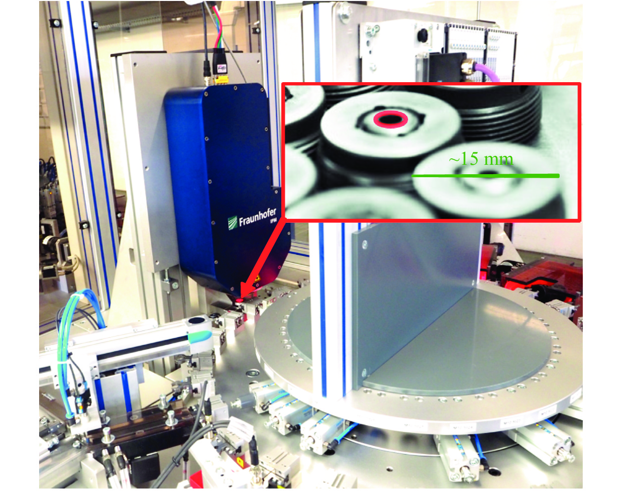
Fig. 4 Photograph of a digital holographic sensor for inline inspection of high-precision sealing surfaces. Inset: representative photograph of samples to be inspected.
The laser sources used in this application were three separately stabilised fibre coupled diode lasers with a free space power output of 30 mW each (Toptica Topmode at 637.68 nm, and Toptica DL100 at 633.31 nm and 633.74 nm). Thus, the synthetic wavelengths used for measurement were 922 µm, 103 µm, and 92 µm.
The inspected surfaces were planes and conical surfaces with tilt angles of up to 20°. A representative photograph of the inspected components is shown in the inset of Fig. 4. The region that will be used to evaluate the data quality is marked with a red ellipse. The peak-to-valley deviations from the ideal shape on the most critical surfaces of such a sample must be smaller than ~10 µm, depending on the sample type. The inspection cycle time was 1 s, including data acquisition and handling time.
The main specifications of the sensor used for this application are listed in Table 1 in the HoloTop 9M column. The field of view of the 18×18 mm2 sensor was sampled with 3072 × 3072 pixels and was slightly larger than the sample diameter.
The output data were filtered using an amplitude-weighted averaging filter with a filter radius of 3 and a median filter of the same size. As the speckle size in the object plane was in the range of 14 µm, we roughly averaged over 2 × 2 speckles for the final result. Using the open-source image processing toolkits OpenCV and PointCloudLibrary, we separated the individual surfaces and borders of each sample. The functional surfaces were defined as two concentric cones and one plane. From each of the three surfaces, a best-fit geometrical description was calculated for the measurement of slope angles and diameters. The maximum positive and negative distances between each pixel of a surface and the best-fit representation allowed the calculation of the peak-to-valley deviation of each surface, which is closely related to the roughness measure PT.
A detail of the height map of one of these samples is shown in Fig. 5a. The grey area represents the points that were assigned to the central surface of the sample. The colour map for the grey values ranges from −15 µm to +15 µm. Pixels that were masked out owing to low interference amplitudes are shown in blue. Pixels assigned to a different surface of the sample are shown in yellow.
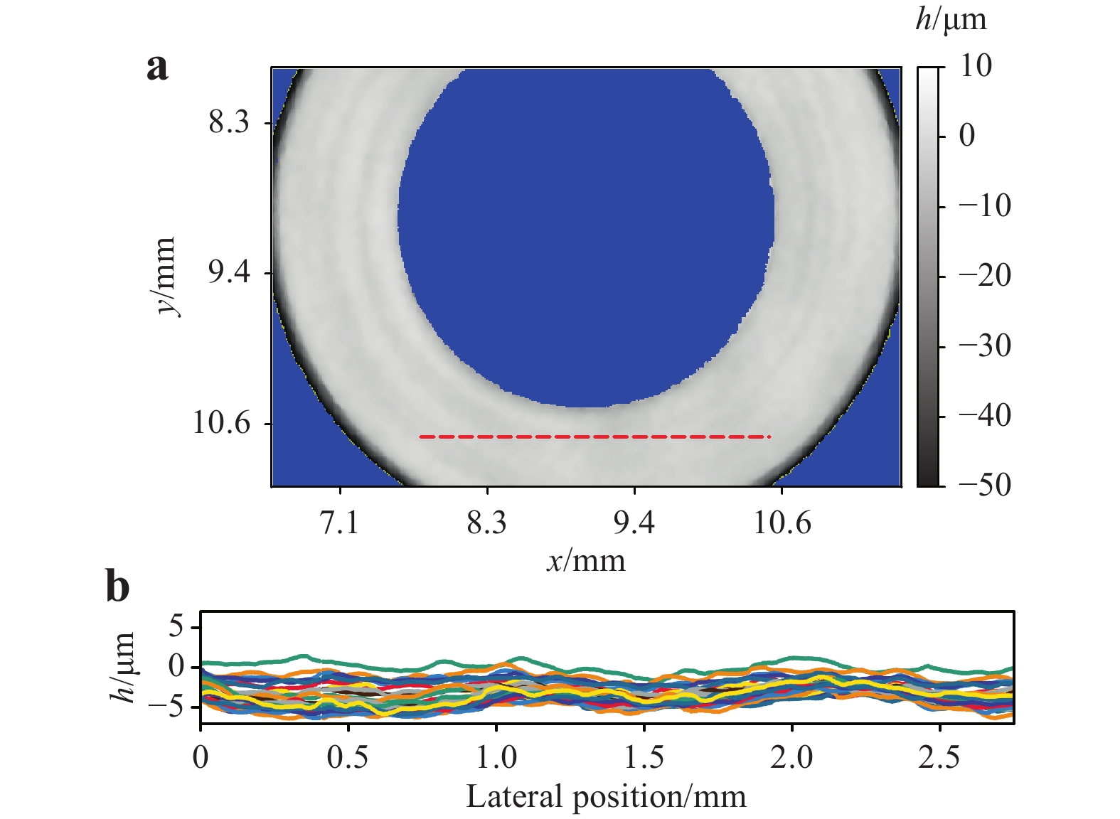
Fig. 5 Measurement results of a sealing sample.
a Detail of the height map of the central surface of the sample. b Cross-section of 25 measurements along the dashed red line in a. For the 25 measurements, the sample was picked up by the handling device and placed back in the measurement position between each of the measurements.The sample was measured 25 times. Between each measurement, the sample was picked up by the handling device, arbitrarily slightly rotated, and returned to the measurement position. In Fig. 5b, the cross sections of the 25 measurements along the dashed red line in (a) are depicted. Although there was no numerical realignment of the data, all measured height values lay within a corridor of +/−2 µm which consists of real surface deviation and misalignment due to handling and measurement accuracy.
From each of these 25 measurements, the peak-to-valley deviation of the surface was calculated. The average value of this deviation was 8.1 µm and the standard deviation of the 25 measurements was 0.45 µm.
For evaluation of long-term stability, the measured values of the feature described above were logged throughout the complete production of one year. During this year, more than 9.8 million measurements were carried out. The measured values of the feature are shown in Fig. 6. Each measured value was plotted in a semi-transparent colour to visualise the distribution of the measured value in a representative way. For display and evaluation, outliers have been removed; peak-to-valley deviations larger than 500 µm cannot be measured realistically because synthetic wavelengths of 1000 µm were used, and these deviations were thus removed (0.02% of all measurements). Such errors appear, for example, if a measurement is performed with a sample placed inaccurately within the field of view or if there is no sample present at all. The black line shows the moving median over 80,000 measurements and the approximate number of measurements per day. The median value of all measured values was 8.3 µm. The median values per day were nearly constant over time and ranged from 7.4 µm to 9.8 µm. Furthermore, for every 80,000 measurements, the measured PT under which 90% of the respective values lay ranged from 10 µm to 16 µm. These values were plotted as dashed lines in Fig. 6 and were within the range of 10.2 µm to 16.5 µm. The tight boundaries in which those values were found indicate that both the production process and the measurement procedure work with high accuracy as process variations of both contribute to the described variations.
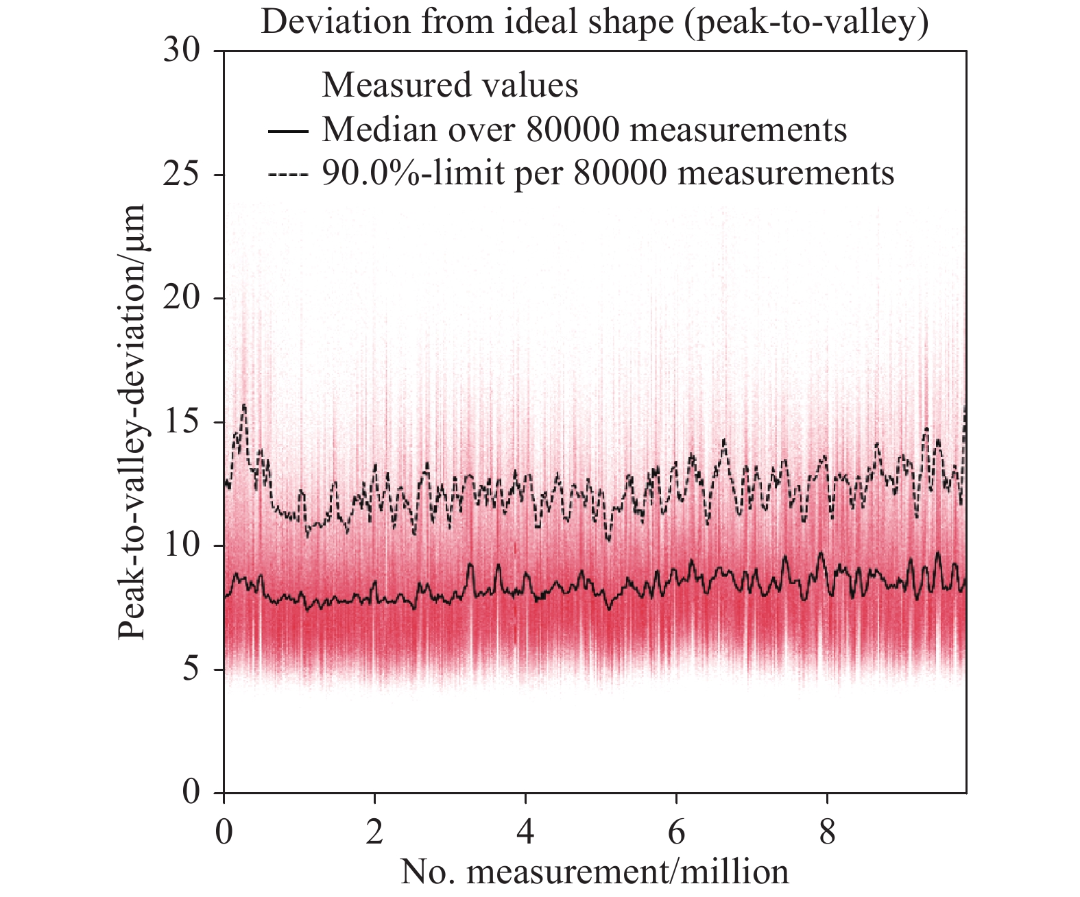
Fig. 6 Measured values for a single feature, peak-to-valley deviations of all data points on one plane surface, over one year. More than 9.8 million parts were measured within that year. All measured values, the median of the measured values over approx. one day (80,000 measurements) and the limit which 90% of all measured values of each day were under are shown.
-
Machine tools are machines for forming or machining metal or other rigid materials and play a key role in production. Current machinery offers production accuracy in the micrometre range; precision machinery even works in the sub-micrometre range27.
However, worn tools, incorrectly calibrated sensors, or poorly chosen trajectories can lead to machining results that do not meet the required specifications28–30.
Therefore, the metrological registration of quality features is an essential part of quality and performance assurance. With a share of almost 90%, geometry inspection (form, dimension, position, and roughness) is highly significant within production metrology. For example, surface topographies, flatness, and microdefects or geometric references of construction elements, such as bores or fittings in the micrometre range, play a major role31.
Monitoring and, if necessary, controlling the processing quality is a complex iterative process that has not been automated to date. Quality control is usually performed on a random basis outside the machine tool in special measuring rooms28–30.
For the measurement of high-precision components, there are no measuring devices that allow direct flat three-dimensional measurements in machine tools31.
Machine tools are complex mechatronic systems that pose a special challenge for high-precision optical measuring systems19, 22.
The HoloPort measuring system developed at Fraunhofer IPM is, to our knowledge, the world's first digital holographic measuring system for direct use in machine tools19.
Owing to the purely mechanical interface of machine tools, the measuring system was designed for wireless operation and is self-sufficient22.
Fig. 7 shows a photograph of the measuring system inside a Hermle C32U 5-axis milling machine at Fraunhofer IPM. The system was mounted on the machine’s HSK 63 tool taper.
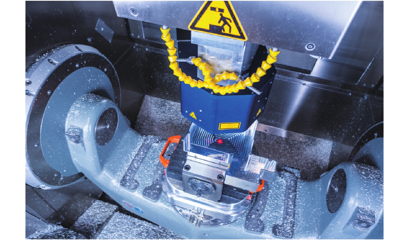
Fig. 7 Inspection of a typical milled surface by HoloPort in a Hermle C32U 5-axis milling machine at Fraunhofer IPM19.
Using the dynamic numerical control (DNC) interface of the machine tool, its axis positions can be read and used for computer-aided design (CAD) comparisons of the measured point cloud. Even complex work pieces can potentially be inspected completely and directly within the machine for the first time—the system becomes a full-field coordinate measuring machine (CMM). The accuracy of a complete point cloud of the surface is mainly limited by the lateral sampling of the system’s camera and the accuracy of the machine tool axes, which are typically in the single micrometre range22.
For the following measurements, two lasers (Ondax LMFC 25–50 mW, linewidth 150–300 MHz) with wavelengths of 632 nm and 640 nm were used, resulting in a synthetic wavelength of 58 µm. The reconstructed data were filtered using a 5 × 5 pixel mean filter. All measurements were taken with the machine axis enabled, but with disabled spindle control in order to minimise disturbing excitations19.
Fig. 8 shows the measurement results of 30 consecutive measurements of the sealing surface of an electric motor housing. A total field of view of 120 × 100 mm with sub-micron precision and lateral sampling of 7 µm was achieved. The cycle was programmed using standard CAD software and converted to an NC program afterwards. The positioning of the measurement fields was chosen so that there was an overlap of approximately 50%, as shown by the black squares. Communication between the machine tool and the measuring system was established via the DNC interface.
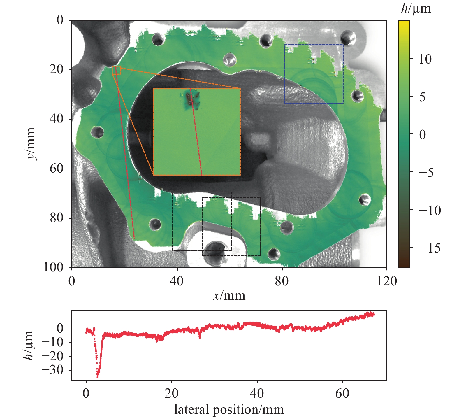
Fig. 8 Stitched measurement, consisting of 30 successively recorded overlapping measurement fields. A total field of view of 120 × 100 mm was recorded with sub-micron precision and lateral sampling of 7 µm. A detailed view (orange) shows the cavity visible in the cross-section.
In the lower half of the image, a section of the measurement data along the red line is visualised. It can be seen that the general flatness of the sealing surface is only a few micrometres, but a flaw in the material extends by approximately 30 µm.
Fig. 9 shows a single measurement of the blue square, marked in the stitched image in Fig. 8.
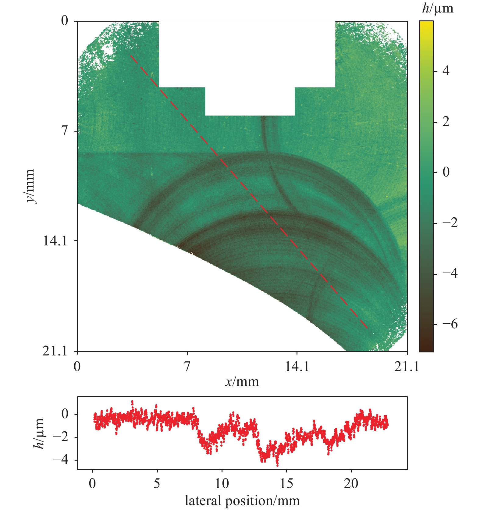
Fig. 9 Single measurement of the stitched measurement data shown in Fig. 8.
In the full-resolution image, one can clearly see several milling traces with a depth in the range of the desired flatness of the sample.
Invalid measurement data such as areas past the measuring object, defocused areas (e.g. the sensor-internal reference target), or weak measuring signals were masked out using white. In the single field of view, this becomes particularly clear in the systematically cut-out areas of the sensor-internal reference target at the upper edge of the image, and the missing data can also be seen for multiple measurements in the stitched data in Fig. 8.
This reference target is used to transform the initial relative measurement data into an absolute scale, if necessary; this reference is not relevant for the flatness within this functional surface but becomes relevant for global references on the part.
Fig. 10 shows one of the two optical planes of the open sensor from below; the reference target and its support stand out through their raw metal appearance.
Fig. 10 View into the downside of the sensor head (without electronics) including internal reference body to measure absolute references in the measuring direction.
Digital holography is unique in that the focal plane can be shifted numerically. This means that even samples with an axial extension far beyond the geometric depth of field of the measuring system can be processed to be evaluated in focus across the whole measurement. Fig. 11 shows the numerically refocused measurement data of the reference target at a distance of ~50 mm from the focal plane of the sensor—the actual sample, being far out of focus, has been masked out in this image. The example cross-sectional view shows a continuous transition with an extension with a height of 350 µm.
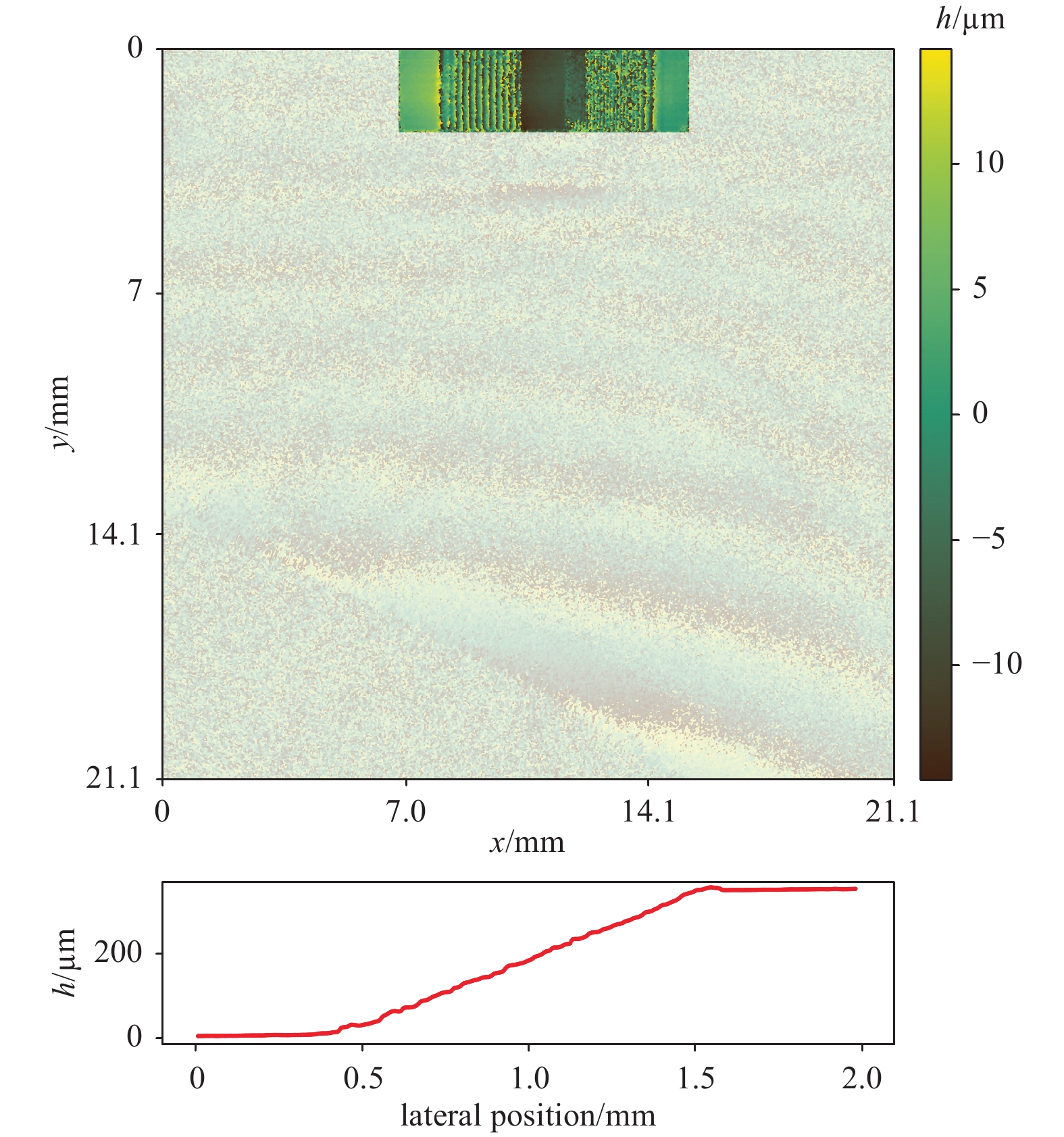
Fig. 11 Numerically refocused reference target with a continuous transition of a height of 350 µm. As the measured part is defocused and shows only noise, it has been masked out using transparency here; only the reference target is fully visible in this view.
In the future, an adapted version of the reference target will allow internal wavelength calibration and observation.
Fig. 12 and Fig. 13 show the reproducibility of the complete measuring system, including the machine tool. The area to be measured was targeted by moving the three linear axes of the machine tool ten times successively. With a specified traversing accuracy of 8 µm (without the commercially available additional package for fine calibration), the machine accuracy was in the range of the lateral sampling of the measuring system, and the measured data were very well aligned. Axially, the measured values deviate from each other in the micrometre range. In addition to the system’s camera, the machine axes, and external disturbing influences such as vibrations, the achievable accuracy depends on the choice of the laser wavelengths and thus the synthetic wavelengths19, 22.
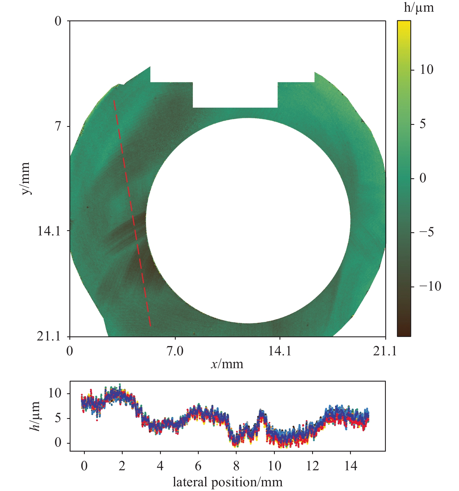
Fig. 12 Illustration of the reproducibility of the measuring system including the machine tool. The area to be measured was targeted by moving the three linear axes of the machine tool ten times successively.
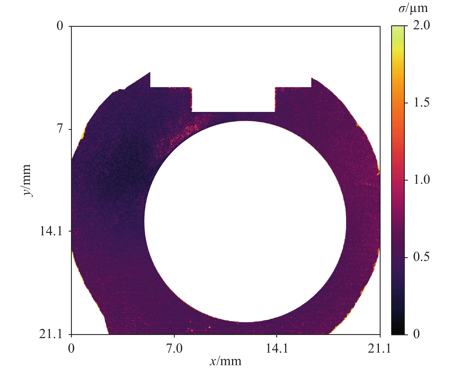
Fig. 13 The standard deviation of the 10 measurements shown in Fig. 12 are mostly below 1 µm. White spaces have been masked, as these areas include either no measuring object or the reference target.
-
One of the most interesting applications of digital holography is the quality control of electronic interconnectors, such as ball grid arrays or microbump structures. State-of-the-art microelectronic devices have tens of thousands to hundreds of thousands of electrical contacts that must be connected using reflow soldering or similar technologies. To ensure a proper connection for all contacts of an interconnector, the electrical contacts of the device must fit tolerances in the single micron range. As the production cycle times of such devices are typically in the range of a few seconds or less, a measurement technology that meets the requirements of inline integration must be able to guarantee both sub-micron repeatability and extremely short measurement duration. In addition to the tight accuracy requirements, the high dynamic range between shiny soldering bumps and rough, dark substrates is challenging for optical measurement approaches.
To achieve a high lateral resolution and fast acquisition speed, the sensor system used for this application was equipped with a 65-megapixel camera and a high-resolution objective lens (focal length 88 mm, magnification
$\beta' $ = −1.66). The sensor system was developed in a joint project with the world’s leading semiconductor manufacturer, Intel Corporation.The laser sources used in this application are three separately stabilised fibre-coupled diode lasers with a free-space power output of 50 mW each (Ondax LMFC, wavelengths: 642.88 nm, 633.82 nm, and 632.915 nm). The synthetic wavelengths used for measurement here are thus 443 µm, 40.9 µm and 40.8 µm. Fig. 14 shows some measurement results of a relevant interconnect sample. Fig. 14a shows the full field of view of the sensor. 10,480 microbumps lie within the field of view and thus were measured in a single measurement. The inset shows a 10x confocal microscope image of a detail of the sample. Fig. 14b shows a detail of (a). Each of the bumps had a diameter of 50 µm and was approximately 20 µm high. The cross-section through the data given below the image shows excellent data quality. To ensure that the measured heights corresponded to the real heights, reference measurements were performed on the same sample using a confocal microscope. Fig. 14c shows the results of this correlation. Here, for each bump, the height measured with the described holographic setup was plotted against the height measured by the reference tool. The mean value of the measured heights was set to zero. The red line illustrates a linear fit to all measured values. The green line corresponds to an ideal correlation between reference data and measured values (i.e. slope = 1). One can easily see the excellent agreement between the two measurements. The correlation coefficient between both data sets is 96.3% and all holographically measured values lie within a corridor of +/−1.0 µm around the respective reference data. To verify the repeatability of the measurement results, ten successive repeat measurements on the depicted sample were carried out. The heights of 99% of all bumps were measured with standard deviations below 0.108 µm. The heights of all bumps within the field of view were measured with standard deviations equal to or less than 0.155 µm.
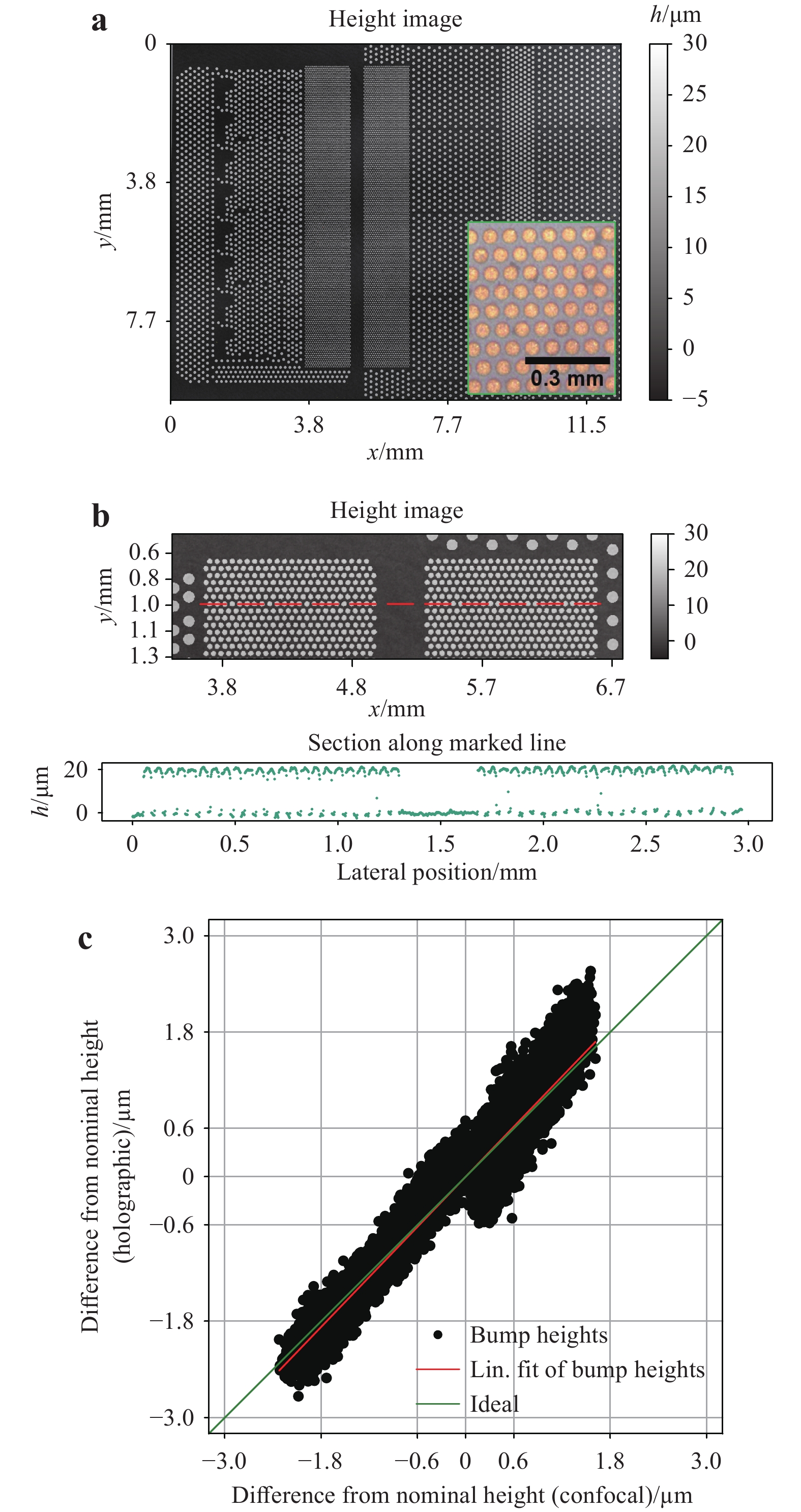
Fig. 14 Measurement results on microbump sample.
a Height image of a BGA; inset: microscope image of the sample. b Detail of a marked with red. c Comparison between holographic data and reference data from a confocal microscope. -
The above use cases show enormous potential for digital holography with multiple wavelengths. No other 3D measurement technology can capture such a large field of view so quickly with comparable lateral sampling and simultaneously with such high axial accuracy.
When applying these technologies to new fields of application, the major challenge of future work is to further reduce the sensitivity of the interferometric technique to external influences such as relative movements between the sensor head and test specimen. Recently published works on holographic topography measurement of continuously moving objects, such as the measurement of gear flanks during the rotation of a gear, are very promising32.
Another bottleneck for wide-ranging industrial applications is the extensively frequency-stabilised laser sources. Because the requirements for measurement accuracy and the unambiguity range vary from application to application, it is still necessary to find and characterise an appropriate laser source (e.g. one with long-term stability)for each wavelength needed. Promising lasers with long-time frequency stabilisation are presented, for example, in the following papers33, 34. However, this is time-consuming and rather uneconomical.
Hence, the current work carried out by Fraunhofer together with the University of Freiburg is concerned with developing a novel light source based on whispering gallery mode resonators. This is intended to enable controlled tuning of the emitted wavelength in the range of 100–300 GHz. For short measurement times, it is necessary to switch between different wavelengths within milliseconds and achieve high reproducibility at the same time.
The goal of all further developments is to open up as many industrial applications as possible on the basis of a common technological platform and to make the technology more reliable and robust. In this context, we want to develop a very compact sensor head for use in multi-axis handling systems such as robots, measuring portals, and coordinate measuring devices.
New manufacturing processes, such as hybrid machining, in which an additively manufactured component is precisely reworked, offer great application potential for process-accompanying measurements using digital holography.
The current unique selling points of the HoloTop family, including robustness, accuracy, and speed, will be further enhanced and extended.
-
We showed that the HoloTop sensor family, which is based on multi-wavelength digital holography, is very powerful for tackling demanding industrial topographic measurement tasks with the highest accuracy requirements. The decisive advantage that distinguishes it from other optical measurement methods and commercially available measurement systems is the short measurement time in relation to the amount of measured 3D points per second. Because the raw data quantity per number of 3D points is less than that of comparable methods such as coherence scanning and laser scanning confocal microscopy, we assume that this intrinsic advantage will be retained and that the technology will continue to assert itself.
The presented measurement results also show that the technique works on reflective and matt surfaces simultaneously. This independence from sample roughness and the capability of measuring even steep flank angles shows universal usability. In our opinion, this point in particular limits the practical application of many other optical measuring methods and is particularly responsible for the fact that tactile measuring technology, which is significantly slower, is still widely used.
The outlook describes which future developments can improve the cost-effectiveness of the technology and which fields of application can be addressed with it.
More generally, the described measurement technology can open up those applications in which large measurement fields in the range of several square centimetres must be detected and tested topographically sib-micrometre accuracy. Especially for inline inspection, the comparatively very short measuring times, well below one second, enable a quantitative 100% inspection in cases where currently only sample testing is possible. The latest applications described in this paper prove this point.
-
The authors would like to thank Werner Gießler GmbH, Elzach, Germany for their partnership during the integration of the prototype measuring system HoloTop into series production and the provision of real production data over the period of an entire year. We also thank the Federal Ministry for Economic Affairs and Energy for financial support as part of the Central Innovation Program for small and medium-sized enterprises (ZIM-KA 3398901 LP4). We also thank Intel Corporation for their great confidence in our developments and permission to publish the measurement data. We are also very grateful for the support provided by the precision mechanical workshop of Fraunhofer IPM for sensor integration into a five-axis machine tool.
Digital holography in production: an overview
- Light: Advanced Manufacturing 2, Article number: 15 (2021)
- Received: 23 January 2021
- Revised: 25 March 2021
- Accepted: 22 May 2021 Published online: 18 June 2021
doi: https://doi.org/10.37188/lam.2021.015
Abstract: Many challenging measurement tasks in production simultaneously have high requirements for accuracy, measurement field size, lateral sampling, and measurement time. In this paper, we provide an overview of the current state of the art in digital holography for surface topography measurements and present three applications from completely different productions with no alternative to digital holography; we describe the HoloTop sensor family, which has been designed specifically for industrial use, and present the most recent results achieved in real-life industrial applications. All applications address measurement tasks that could not be solved until now, either by optical or tactile means. We start with a description of the first-ever inline integration of a digital holographic measurement system that inspects precision turned parts for the automotive industry. We proceed by presenting measurements performed with a compact sensor that can be placed inside a tooling machine and operated fully wirelessly. In this case, the tool holder was used to position the sensor directly. Integration into a tooling machine places high demands on both robustness and reliability. Finally, the quality control of electronic interconnectors such as microbumps with the highest demand for accuracy and repeatability is demonstrated. All of these applications illustrate the major advantages of digital holographic systems: it is possible to measure a relatively large field of view with interferometric precision and very short acquisition times. Additionally, both reflective and matt surfaces can be measured simultaneously. We end this publication with an assessment of the future potential of this technology and the necessary development steps involved.
Research Summary
Digital Holography: The next generation of inline 3D measurement
Over the last decade, digital holography has become one of the fastest and at the same time most accurate methods for surface topography in production lines. The basic measurement principle uses interferometric recording of light waves reflected from component surfaces. By clever use of several lasers with different wavelengths, also macroscopic objects can be measured with sub-micrometer accuracy. Scientists at Fraunhofer Institute for Physical Measurement Techniques now give an overview of industrial applications that demonstrate the unique selling point of the technology for optical inline measurements of macroscopic measurement fields with sub-micron accuracy. Despite the high sensitivity to external influences such as vibrations, the implementation of holographic sensors in production environments has been very successful. Industrial applications in metal processing and chip manufacturing prove this impressively.

Rights and permissions
Open Access This article is licensed under a Creative Commons Attribution 4.0 International License, which permits use, sharing, adaptation, distribution and reproduction in any medium or format, as long as you give appropriate credit to the original author(s) and the source, provide a link to the Creative Commons license, and indicate if changes were made. The images or other third party material in this article are included in the article′s Creative Commons license, unless indicated otherwise in a credit line to the material. If material is not included in the article′s Creative Commons license and your intended use is not permitted by statutory regulation or exceeds the permitted use, you will need to obtain permission directly from the copyright holder. To view a copy of this license, visit http://creativecommons.org/licenses/by/4.0/.

 DownLoad: