


-
Model-based optical scatterometry is an indirect measurement technique for characterising complex periodic nanostructures with feature dimensions below the resolution limit of visible-wavelength microscopy1,2. In contrast to its competing direct measurement technologies, scanning electron microscopy and atomic force microscopy, optical scatterometry has the advantages of a contact-free and non-destructive operation mode, high throughput, and integrability, making it suitable for in situ process control in high-volume semiconductor manufacturing. By comparing the measured and modelled signatures and searching for the best match, the parameter values of a structure are determined indirectly1. Scatterometry, hence, provides a solution to an inverse problem.
Owing to the unabating demand for higher transistor density and improved functionality, the structures on semiconductor chips not only continued to shrink over the years, but they also became three-dimensional and more complex. Accurate modelling of modern nanostructuresrequires large parameter spaces with a multitude of parameters, as well as a priori knowledge about the design of each structure and the corresponding fabrication process. Owing to these large parameter spaces, the inherently ill-posed inverse problem of scatterometry becomes even more difficult to solve, and the reconstruction often fails because of insufficient sensitivities towards certain parameters or large cross-correlations between them. Therefore, it is common practice to reduce the number of free parameters by fixing or neglecting some of them during model-based reconstruction3. Even though these parameters are carefully selected based on either experience or a preceding sensitivity analysis, large errors may be ecountered3.
Because a limited parameter space is generally not feasible owing to erroneous reconstruction results, a way must be found to make the full parameter space available instead. To that end, the ambiguities of the inverse problem must be reduced by regularising it in a more stable manner. This may be achieved by adapting the scatterometric sensor itself to provide the maximum amount of uncorrelated measurement data. The light field contains a variety of different information channels, including intensity, wavelength, phase, propagation angle, polarisation, and coherence. If the information content is to be maximised, the sensor should employ as many channels as possible.
The earliest versions of scatterometers, namely, the angular4 and the spectroscopic5 scatterometer, only used two information channels of the light field each: the intensity plus either the detection angle or the wavelength. Since then, the information content has been methodically increased by developing new setup variants, including, without being limited to, goniometric ultraviolet scatterometry6, coherent Fourier scatterometry7, Fourier ellipsometry8,9, Mueller-matrix spectroscopic ellipsometry10,11, angular Mueller polarimetry in conical diffraction12,13, and white-light interference approaches2,14. This list suggests that, besides the intensity, the three most important information channels are the wavelength, propagation angle, and state of polarisation, but none of the techniques mentioned before makes full use of all of these channels at the same time, that is, none of them provides the full Mueller matrix with simultaneous angle and wavelength resolution.
To evaluate and quantify the benefits of individual information channels, we performed a comprehensive sensitivity analysis based on rigorous simulations. This study considered a wide range of sub-wavelength gratings covering typical problems of current process control in semiconductor manufacturing, including large parameter spaces, isolated structures, linewidths in the single-digit and small two-digit nanometre range, structural asymmetries on the nanoscale, and unknown variations of the refractive indices. For detailed results, the reader is referred to ref. 15. In short, the findings of this study may be summarised as follows: In the case of complex multi-parameter problems, approaches based on the Mueller matrix always outperform others in terms of lower measurement uncertainties and cross-correlations. In some use cases, spectroscopic Mueller polarimetry under an optimised angle of incidence proves to be more powerful, whereas in others, angular Mueller polarimetry at an optimised wavelength achieves the best results. To enable maximum flexibility towards all kinds of targets, the ideal sensor should provide the angle- and wavelength-resolved Mueller matrix of the sample and, if at all, this data range should only be restricted numerically during post-processing. If the entire range is used for the reconstruction instead, the measurement uncertainties are typically slightly larger than those obtained with the optimised subsets, but in general, the results still meet the sensitivity criteria and no a priori knowledge is required.
In view of the above, we recently proposed a new scatterometric method called white-light Mueller-matrix Fourier scatterometry15. In short, we combined the well-known techniques of white-light interferometry, Mueller polarimetry, and Fourier scatterometry into one apparatus. It enables the measurement of both angle- and wavelength-resolved Mueller matrices and, hence, simultaneously covers all three key information channels. Starting from the encouraging simulation results discussed above, we implemented a prototype version of the sensor. In ref. 15, we were only able to show some experimental results from a very early stage of the sensor assembly and calibration. Since then, we have completed the implementation, and we are now in a position to demonstrate the practical feasibility of our approach for real metrology tasks, exemplified by the model-based reconstruction of a sub-wavelength silicon line grating.
-
In this section, we first introduce the experimental setup. The sensor’s most important sub-functionalities are validated by means of some basic proof-of-principle measurements. Subsequently, we explain the overall measurement strategy. The mathematical details of the sensor calibration and polarimetric analysis will be covered in Section 3.
Our setup is essentially a combination of a Fourier-plane microscope, a Fourier-transform spectrometer based on a Linnik interferometer, and a polarimeter. A schematic drawing and a photograph of the experimental setup are shown in Figs. 1 and 2, respectively.
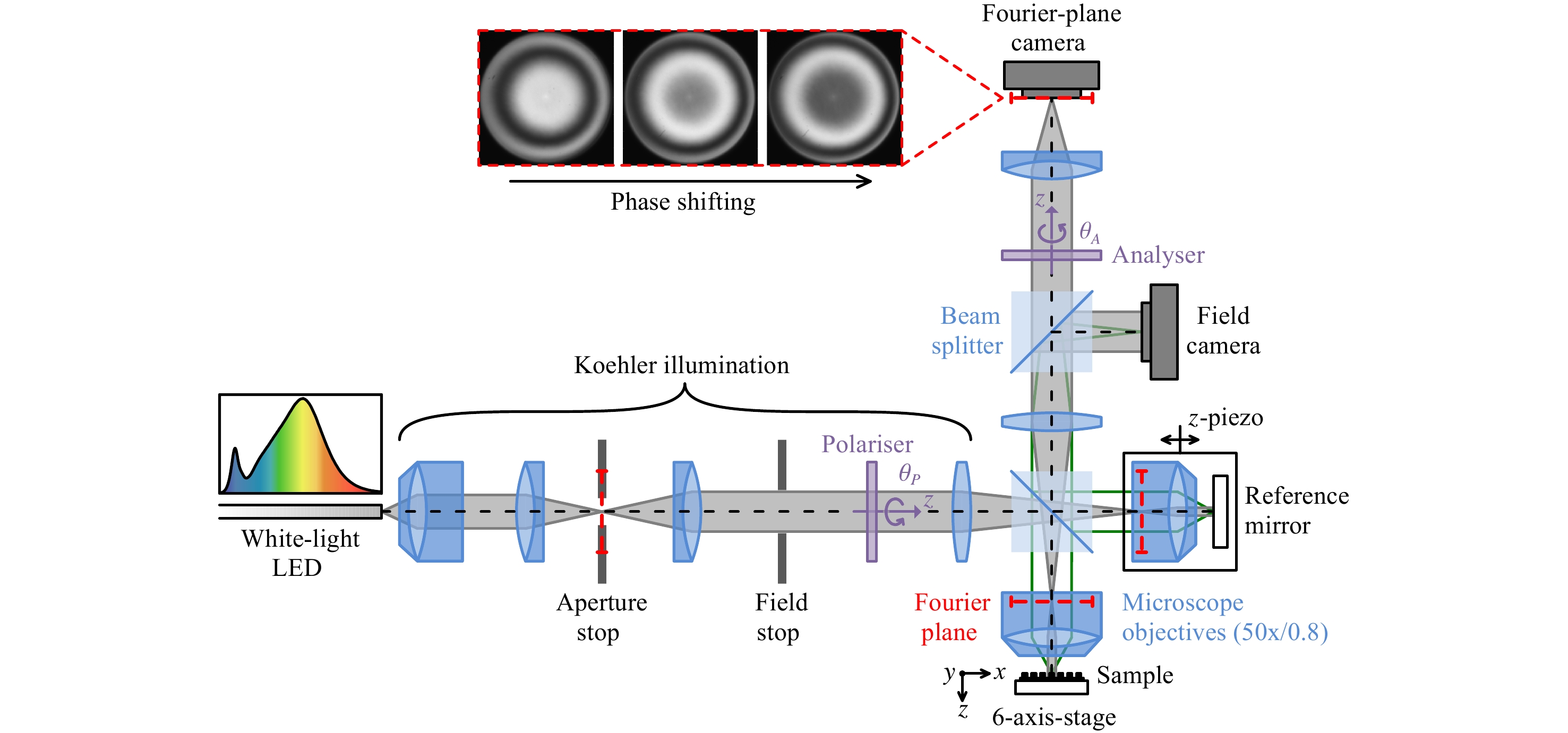
Fig. 1 Schematic of the sensor.
Both the polariser and the analyser can be rotated around the optical axis. The inset shows exemplary measured images of the angle-resolved Fourier plane during a$ z $ 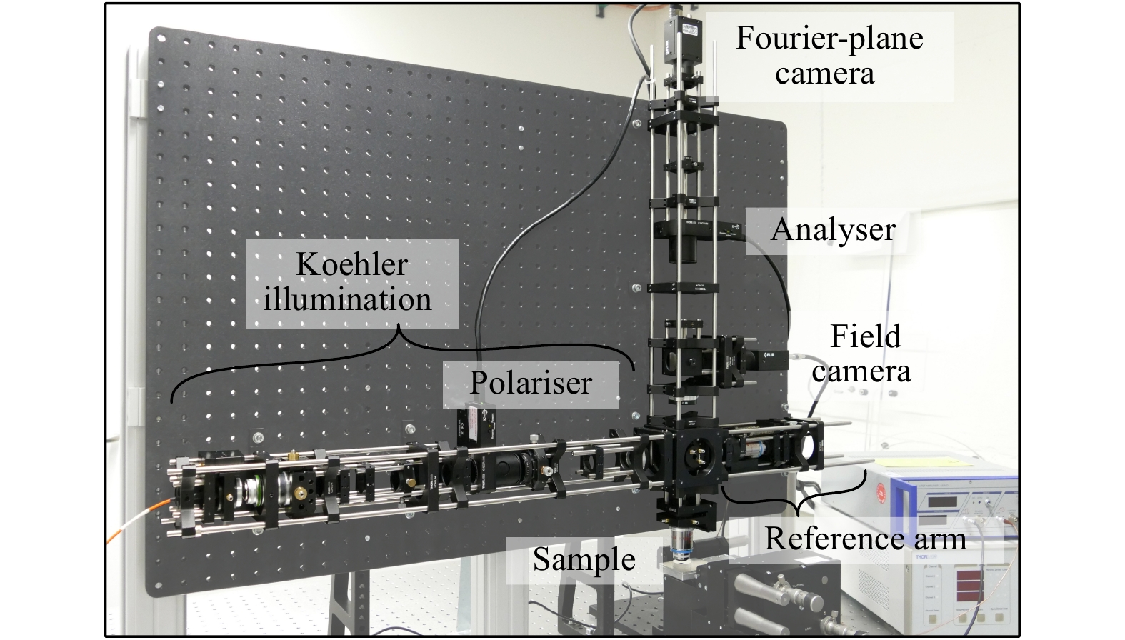
Fig. 2 Photograph of the experimental setup.
Without the reference arm and the analyser, the setup is a standard microscopic arrangement with Koehler illumination and two detection channels. Light from a broadband, white-light LED (covering a spectral range from 400 to 800 nm) is coupled into the system via a multimode fibre. A Glan-Taylor prism selects a linear state of polarisation, characterised by the rotation angle
$ {\theta }_{P} $ around the optical$ z $ -axis. The fibre core is magnified in two steps and imaged into the back-focal plane of the microscope objective above the sample. We use a strain-free microscope objective (EC Epiplan-Neofluar Pol from ZEISS, Jena, Germany) with 50 × magnification and a numerical aperture (NA) of 0.8. The objective’s exit pupil diameter is slightly smaller than the final image of the fibre core, which ensures that the available NA can be fully utilised in the experiments. To allow for easy positioning of the targets, the sample is mounted on a 6-axis stage. If necessary, the field of view can be adapted by the field stop to underfill the target size. For monitoring purposes, the sample surface is imaged onto the so-called field camera (see Fig. 1). The actual measurement channel is provided by the Fourier-plane camera, which records images of the back-focal (or Fourier) plane of the microscope objective. Both cameras are of the type Grasshopper 3 from FLIR (Richmond, Canada) with monochrome CMOS sensors.In the Fourier plane, the individual propagation angles are spatially resolved16, that is, each camera pixel corresponds to a specific combination of incidence angle
$ \alpha $ and azimuth angle$ \varphi $ (see Fig. 3). The entire angular spectrum is, hence, recorded in one shot without the need for mechanical scanning. Typically, the angle combinations are expressed in terms of the NA coordinates$ {NA}_{x} $ in$ x $ -direction and$ {NA}_{y} $ in$ y $ -direction (see Fig. 3a). The maximum NA is 0.8, which limits the angle of incidence$ \alpha $ to approximately 53°.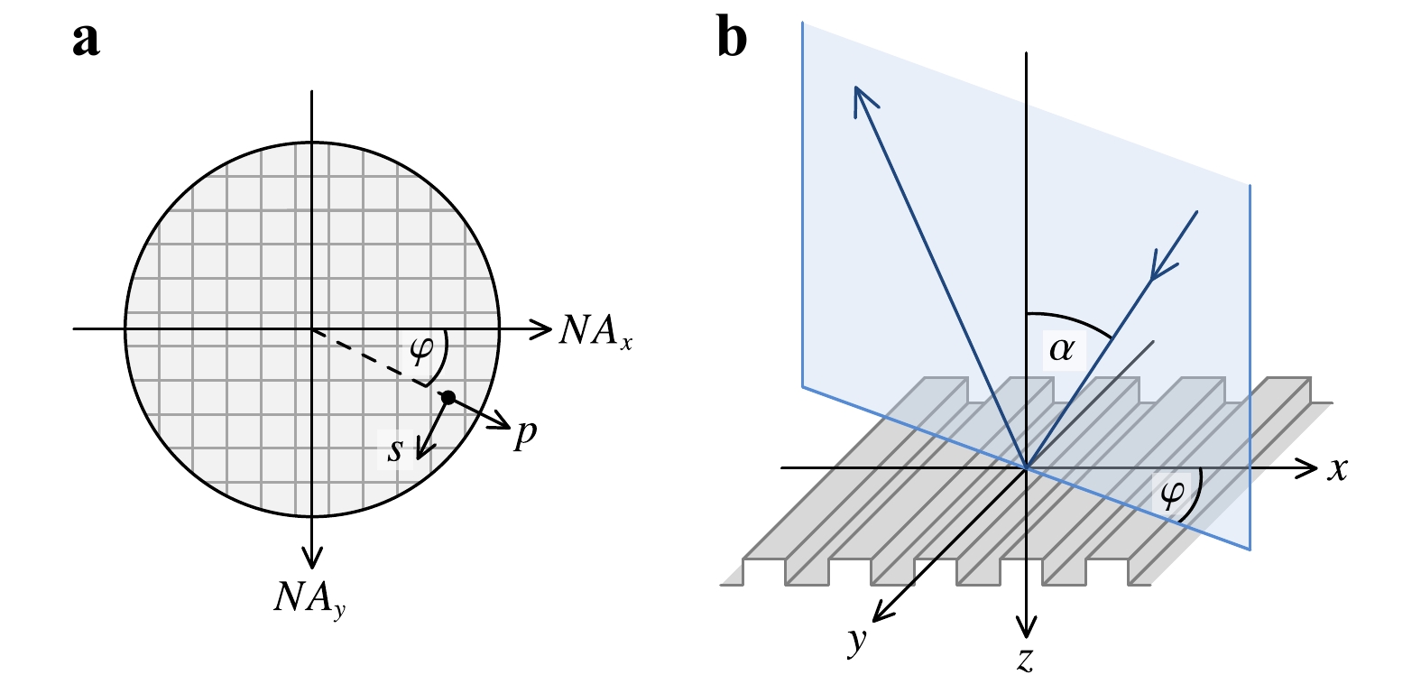
Fig. 3 Coordinate systems.
a Coordinate system in the Fourier plane. The aperture is sampled by a quadratic grid of$ {NA}_{x} $ $ {NA}_{y} $ $ p $ $ s $ $ \varphi $ $ \varphi $ $ \alpha $ By means of a simple experiment without the analyser and the reference arm, it is straightforward to verify that our sensor correctly images the angularly resolved Fourier plane. As the sample reflectivity varies with the angle of incidence and the state of polarisation, we expect distinct Fourier-plane intensity signatures even on simple targets. Fig. 4a shows two exemplary measurements with different polariser orientations on an unstructured plane silicon wafer. The 90° rotation of the polariser between the two measurements causes nothing but a 90° rotation of the image because the sample is isotropic. Keep in mind that without the reference arm, it is not yet possible to separate the individual wavelengths. To remove the spatially inhomogeneous illumination profile, each measurement performed on the silicon wafer was divided through a reference measurement on a silver mirror. Furthermore, a dark-current image was subtracted. In principle, this basic calibration routine was also applied to the full Mueller matrix measurement, but we used a different reference target and performed additional phase corrections. A detailed explanation is provided in Section 3.
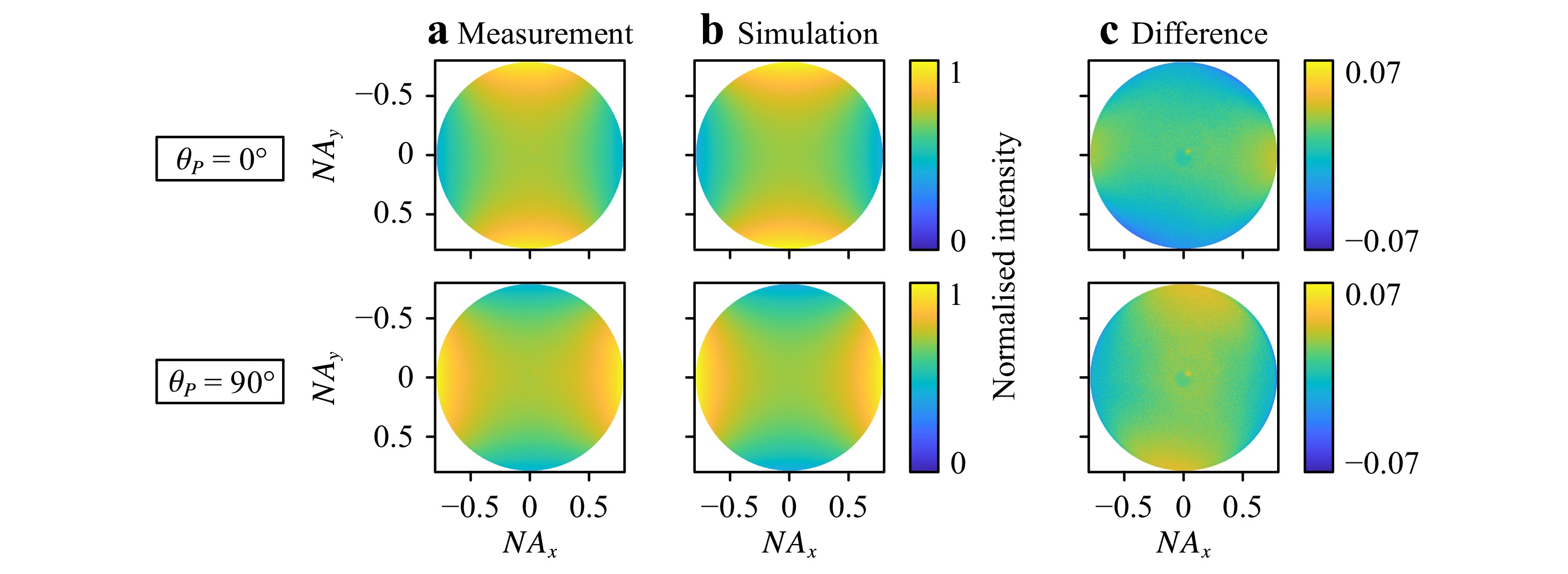
Fig. 4 Fourier-plane white-light intensity distributions generated by a plane silicon wafer, using different rotation angles
$ {\mathit{\theta }}_{\mathit{P}} $ of the polariser.a Normalised measurement results, obtained without analyser and reference arm; b normalised simulation results; c difference between measurement and simulation.Fig. 4b depicts the simulated intensity distributions in the Fourier plane, taking into account the source spectrum from Fig. 1 and a 3-nm thick native oxide layer (value determined using a commercial ellipsometer). For details on the simulation environment, the reader is referred to Section 4. Finally, the difference between measurement and simulation is plotted in Fig. 4c. The match is excellent, with the root-mean-square (RMS) being as low as 1.6% (2.3%) for θP = 0° (90°).
The two difference images in Fig. 4c are rotated by approximately 90° with respect to each other. Additionally, the angular dependence of each of the difference images is roughly reversed with respect to the two original images in Figs. 4a, b. On the basis of these observations, we conclude that the remaining deviations between measurement and simulation are most likely due to imperfect polarisation: First, the extinction ratio of the polariser is not infinitely large, and second, scattering may occur somewhere in the setup, both of which lead to polarisation components not taken into account in the simulations.
To separate the individual wavelengths using Fourier-transform spectroscopy, it is necessary to record white-light interference signals. Our Linnik-type reference arm uses a protected silver reference mirror and a second microscope objective, which is nominally identical to that in the object arm. We chose the Linnik-type interferometer over the classical Michelson and Mirau variants to enable a large NA and the use of off-the-shelf strain-free microscope objectives. Potential disadvantages of this approach include a less compact design, higher calibration demands, and increased sensitivity to environmental influences, such as vibrations. However, we believe that the advantage of the large NA outweighs the disadvantages because we know from our simulation study that large angles of incidence are particularly beneficial for model-based reconstruction15.
Phase shifting is realised by translating the whole reference arm, that is, both the microscope objective and the reference mirror, along the optical axis in the
$ z{\text -}{\rm{direction.}} $ The total scan length typically exceeds the coherence length of the light source. At each scan position$ z $ , one image of the Fourier plane is recorded, as shown in the inset of Fig. 1. This image series$ I\left({NA}_{x},{NA}_{y},z\right) $ is evaluated pixel-wise. An exemplary measured interferogram$ I\left(z\right) $ from one pixel$ \left({NA}_{x},{NA}_{y}\right) $ is shown in Fig. 5a, using a silver mirror as the sample. We employed a step size of 22 nm for this measurement and recorded a total of 800 images, which corresponds to a scan length$ {L}_{\mathrm{s}\mathrm{c}\mathrm{a}\mathrm{n}} $ of 17.6 µm. By applying a fast Fourier transform (FFT) and considering the absolute value$ \left|\mathrm{FFT}\left(I\left(z\right)\right)\right|=\left|\tilde {I}\left(\lambda \right)\right| $ , the spectrum is retrieved, as shown in Fig. 5b (blue circles). The wavelength resolution ranges between$ {\left({\lambda }^{\mathrm{m}\mathrm{i}\mathrm{n}}\right)}^{2}/2{L}_{\mathrm{s}\mathrm{c}\mathrm{a}\mathrm{n}}\approx $ 4.5 nm and$ {\left({\lambda }^{\mathrm{m}\mathrm{a}\mathrm{x}}\right)}^{2}/2{L}_{\mathrm{s}\mathrm{c}\mathrm{a}\mathrm{n}}\approx $ 18.2 nm, where$ {\lambda }^{\mathrm{m}\mathrm{i}\mathrm{n}} $ and$ {\lambda }^{\mathrm{m}\mathrm{a}\mathrm{x}} $ are the minimum and maximum wavelengths, respectively. If finer sampling in the wavelength space is desired, the scan length must be increased. Currently, the selected piezo scanner limits the available scan length to 100 µm. The step size may be as large as 100 nm without changing the spectral resolution or obstructing the measurement.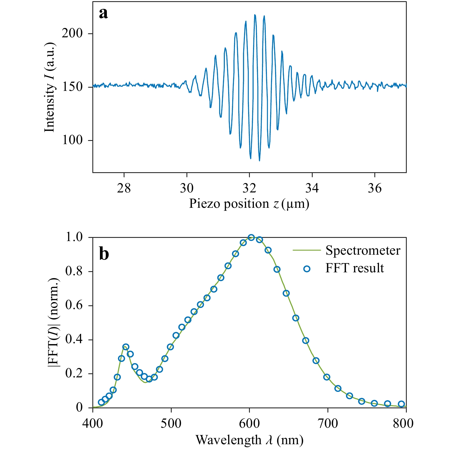
Fig. 5 Exemplary measured white-light interference signal and the corresponding spectrum.
a Intensity I in one pixel of the Fourier-plane camera as a function of the piezo-scanner position$ z $ For comparison, we also measured the spectrum using a commercial spectrometer (solid green line in Fig. 5b). The two datasets match very well, thus confirming the capability of our setup to retrieve wavelength-resolved information from white-light interferograms. Note that the wavelengths are separated numerically by an FFT in post-processing instead of being separated spatially by an additional optical component such as a diffraction grating or a dispersive prism. Consequently, the resolution of the two-dimensional detector in the Fourier plane is fully dedicated to angles and not wavelengths.
It should be emphasised that the Fourier transform actually provides complex numbers
$ \tilde {I}\left(\lambda \right) $ , that is, information not only on the absolute value as a function of wavelength, but also on the phase angle. By successively evaluating each camera pixel, we obtain the complex image stack$ \tilde {I}\left({NA}_{x},{NA}_{y},\lambda \right) $ . To remove the inhomogeneous illumination profile and all constant phase aberrations from this image stack, it is necessary to perform an additional reference measurement on a well-known target. As already mentioned, this calibration procedure is covered in detail in Section 3. The result of the calibration is the complex electric field$ E\left({NA}_{x},{NA}_{y},\lambda \right) $ .For the polarimetric analysis, we assume that the setup and sample are non-depolarising. The interferometric signal generation can then be fully described by Jones calculus, where each element of the setup is characterised by a complex 2 × 2 Jones matrix. The four coefficients of the Jones matrix
$ J $ of the sample are determined in the measurement, whereas all other coefficients are eliminated by the calibration routine. Solving for four unknowns generally requires four equations, that is, four measurements of E using different angular orientations$ \left({\theta }_{P},{\theta }_{A}\right) $ of polariser and analyser. Based on$ J $ , it is straightforward to calculate the 4 × 4 real-valued Mueller matrix M of the sample, which is used as input for the model-based reconstruction. The choice of suitable angular positions of the polariser and analyser will be discussed in Section 3, together with the necessary equations for calculating both matrices from the calibrated measurement results E. The final result, that is, the measured Mueller matrix$ M\left({NA}_{x},{NA}_{y},\lambda \right) $ of an exemplary nanostructure, will be shown in Section 5. -
Calibration is indispensable for the sensor operation. Without calibration, the generally inhomogeneous spatial illumination profile and the phase aberrations of the system would by far dominate the subtle intensity and phase profile changes caused by dimensional variations of typical nanostructures. Our calibration routine comprises two steps: first, referring to a well-known, typically unstructured target, and second, removing defocus and tilt phase terms by means of a Zernike decomposition of the phase map. In view of the subsequent polarimetric analysis, the latter step is especially important because it establishes correct relative phase relationships in a series of measurements.
-
Per wavelength
$ \lambda $ and propagation angle$ \left({NA}_{x},{NA}_{y}\right) $ , the interaction between the object and reference arm is a simple two-beam interference:$$ {I}_{2\mathrm{b}}={I}_{\mathrm{o}\mathrm{b}\mathrm{j}}+{I}_{\mathrm{r}\mathrm{e}\mathrm{f}}+2\sqrt{{I}_{\mathrm{o}\mathrm{b}\mathrm{j}} \; {I}_{\mathrm{r}\mathrm{e}\mathrm{f}}} \; \mathrm{cos}\left(\frac{4\pi z}{\lambda }+{\phi }_{\mathrm{r}\mathrm{e}\mathrm{f}}-{\phi }_{\mathrm{o}\mathrm{b}\mathrm{j}}\right) $$ (1) In this equation,
$ z $ is the scan position of the reference arm, and$ \Delta \phi =4\pi z/\lambda +{\phi }_{\mathrm{r}\mathrm{e}\mathrm{f}}-{\phi }_{\mathrm{o}\mathrm{b}\mathrm{j}} $ describes the phase difference between the reference and test waves. The phase$ {\phi }_{\mathrm{o}\mathrm{b}\mathrm{j}}={\phi }_{\mathrm{t}\mathrm{a}\mathrm{r}\mathrm{g}\mathrm{e}\mathrm{t}}+{\phi }_{\mathrm{p}\mathrm{a}\mathrm{t}\mathrm{h},\mathrm{o}\mathrm{b}\mathrm{j}} $ consists of two summands: the actual target phase$ {\phi }_{\mathrm{t}\mathrm{a}\mathrm{r}\mathrm{g}\mathrm{e}\mathrm{t}} $ , and a general phase term$ {\phi }_{\mathrm{p}\mathrm{a}\mathrm{t}\mathrm{h},\mathrm{o}\mathrm{b}\mathrm{j}} $ which considers all constant phase shifts associated with the object-arm path through the optical system, such as the aberrations of the microscope objective in the object arm. Phase$ {\phi }_{\mathrm{r}\mathrm{e}\mathrm{f}} $ is defined analogously, with the reference mirror acting as the target:$ {\phi }_{\mathrm{r}\mathrm{e}\mathrm{f}}={\phi }_{\mathrm{m}\mathrm{i}\mathrm{r}\mathrm{r}\mathrm{o}\mathrm{r}}+{\phi }_{\mathrm{p}\mathrm{a}\mathrm{t}\mathrm{h},\mathrm{r}\mathrm{e}\mathrm{f}} $ . Intensity$ {I}_{\mathrm{o}\mathrm{b}\mathrm{j}} $ contains the intensity response of the target$ {I}_{\mathrm{t}\mathrm{a}\mathrm{r}\mathrm{g}\mathrm{e}\mathrm{t}} $ itself, and a unitless factor$ {\Sigma }_{\mathrm{i}\mathrm{l}\mathrm{l}\mathrm{u}} $ which accounts for the spatial variation of the illumination profile in the Fourier plane:$ {I}_{\mathrm{o}\mathrm{b}\mathrm{j}}={\Sigma }_{\mathrm{i}\mathrm{l}\mathrm{l}\mathrm{u}} \cdot {I}_{\mathrm{t}\mathrm{a}\mathrm{r}\mathrm{g}\mathrm{e}\mathrm{t}} $ . In a complete analogy,$ {I}_{\mathrm{r}\mathrm{e}\mathrm{f}} $ is defined as$ {I}_{\mathrm{r}\mathrm{e}\mathrm{f}}={\Sigma }_{\mathrm{i}\mathrm{l}\mathrm{l}\mathrm{u}} \cdot {I}_{\mathrm{m}\mathrm{i}\mathrm{r}\mathrm{r}\mathrm{o}\mathrm{r}} $ . We want to emphasise that all quantities are angle- and wavelength-dependent, whereas only$ {\Delta }\phi $ depends on$ z $ .The integral over all two-beam interference terms
$ {I}_{2\mathrm{b}} $ from Eq. 1 within the spectral range of the source corresponds to the white-light interference signal$ I\left(z\right) $ per angle (see Fig. 5a). To remove spatially inhomogeneous coherence effects, each measured interferogram is normalised by its contrast$ C $ , which is defined as$ C=\left({I}^{\mathrm{m}\mathrm{a}\mathrm{x}}-{I}^{\mathrm{m}\mathrm{i}\mathrm{n}}\right)/\left({I}^{\mathrm{m}\mathrm{a}\mathrm{x}}+{I}^{\mathrm{m}\mathrm{i}\mathrm{n}}\right) $ . The maximum and minimum intensity values$ {I}^{\mathrm{m}\mathrm{a}\mathrm{x}} $ and$ {I}^{\mathrm{m}\mathrm{i}\mathrm{n}} $ are determined by fitting envelopes to the white-light signal. Subsequently, the FFT is applied. When evaluated at a single wavelength, the complex result17 of the FFT is:$$ {\tilde {I}}_{1}=2{\Sigma }_{\mathrm{i}\mathrm{l}\mathrm{l}\mathrm{u}}\sqrt{{I}_{\mathrm{t}\mathrm{a}\mathrm{r}\mathrm{g}\mathrm{e}\mathrm{t}}{I}_{\mathrm{m}\mathrm{i}\mathrm{r}\mathrm{r}\mathrm{o}\mathrm{r}}} \cdot {\mathrm{e}}^{\mathrm{i}\left({\phi }_{\mathrm{m}\mathrm{i}\mathrm{r}\mathrm{r}\mathrm{o}\mathrm{r}}+{\phi }_{\mathrm{p}\mathrm{a}\mathrm{t}\mathrm{h},\mathrm{r}\mathrm{e}\mathrm{f}}-{\phi }_{\mathrm{t}\mathrm{a}\mathrm{r}\mathrm{g}\mathrm{e}\mathrm{t}}-{\phi }_{\mathrm{p}\mathrm{a}\mathrm{t}\mathrm{h},\mathrm{o}\mathrm{b}\mathrm{j}}\right)} $$ (2) The first two summands from Eq. 1 disappear because they are independent of
$ z $ .As we are only interested in the target properties, we have to extract
$ {I}_{\mathrm{t}\mathrm{a}\mathrm{r}\mathrm{g}\mathrm{e}\mathrm{t}} $ and$ {\phi }_{\mathrm{t}\mathrm{a}\mathrm{r}\mathrm{g}\mathrm{e}\mathrm{t}} $ from Eq. 2. For this purpose, we perform a second measurement on a calibration target and obtain$$ {\tilde {I}}_{2}=2{\Sigma }_{\mathrm{i}\mathrm{l}\mathrm{l}\mathrm{u}}\sqrt{{I}_{\mathrm{c}\mathrm{a}\mathrm{l}\mathrm{i}\mathrm{b}}{I}_{\mathrm{m}\mathrm{i}\mathrm{r}\mathrm{r}\mathrm{o}\mathrm{r}}} \cdot {\mathrm{e}}^{\mathrm{i}\left({\phi }_{\mathrm{m}\mathrm{i}\mathrm{r}\mathrm{r}\mathrm{o}\mathrm{r}}+{\phi }_{\mathrm{p}\mathrm{a}\mathrm{t}\mathrm{h},\mathrm{r}\mathrm{e}\mathrm{f}}-{\phi }_{\mathrm{c}\mathrm{a}\mathrm{l}\mathrm{i}\mathrm{b}}-{\phi }_{\mathrm{p}\mathrm{a}\mathrm{t}\mathrm{h},\mathrm{o}\mathrm{b}\mathrm{j}}\right)} $$ (3) from the FFT (at the same angle and wavelength as before). Next, we divide Eq. 2 by Eq. 3 to eliminate the influence of the reference arm, that is, quantities
$ {I}_{\mathrm{m}\mathrm{i}\mathrm{r}\mathrm{r}\mathrm{o}\mathrm{r}} $ ,$ {\phi }_{\mathrm{m}\mathrm{i}\mathrm{r}\mathrm{r}\mathrm{o}\mathrm{r}} $ , and$ {\phi }_{\mathrm{p}\mathrm{a}\mathrm{t}\mathrm{h},\mathrm{r}\mathrm{e}\mathrm{f}} $ . Furthermore, the illumination factor$ {\Sigma }_{\mathrm{i}\mathrm{l}\mathrm{l}\mathrm{u}} $ and the general phase contribution$ {\phi }_{\mathrm{p}\mathrm{a}\mathrm{t}\mathrm{h},\mathrm{o}\mathrm{b}\mathrm{j}} $ from the path through the object arm vanish:$$ \frac{{\tilde {I}}_{1}}{{\tilde {I}}_{2}}=\frac{\sqrt{{I}_{\mathrm{t}\mathrm{a}\mathrm{r}\mathrm{g}\mathrm{e}\mathrm{t}}}}{\sqrt{{I}_{\mathrm{c}\mathrm{a}\mathrm{l}\mathrm{i}\mathrm{b}}}} \cdot {\mathrm{e}}^{\mathrm{i}\left({\phi }_{\mathrm{c}\mathrm{a}\mathrm{l}\mathrm{i}\mathrm{b}}-{\phi }_{\mathrm{t}\mathrm{a}\mathrm{r}\mathrm{g}\mathrm{e}\mathrm{t}}\right)} $$ (4) The calibration target is simple and well-known, such that
$ {I}_{\mathrm{c}\mathrm{a}\mathrm{l}\mathrm{i}\mathrm{b}} $ and$ {\phi }_{\mathrm{c}\mathrm{a}\mathrm{l}\mathrm{i}\mathrm{b}} $ can be removed from Eq. 4, using either simulation or additional measurements. For the model-based reconstruction presented in this study, we use a combination of both approaches. Our calibration target is an unstructured plane silicon wafer. We measure$ {I}_{\mathrm{c}\mathrm{a}\mathrm{l}\mathrm{i}\mathrm{b}} $ in the same way as the intensity distributions shown in Fig. 4a and multiply the results from Eq. 4 with$ \sqrt{{I}_{\mathrm{c}\mathrm{a}\mathrm{l}\mathrm{i}\mathrm{b}}} $ to obtain the preliminary measurement results, E:$$ E=\frac{{\tilde {I}}_{1}}{{\tilde {I}}_{2}} \cdot \sqrt{{I}_{\mathrm{c}\mathrm{a}\mathrm{l}\mathrm{i}\mathrm{b}}}=\sqrt{{I}_{\mathrm{t}\mathrm{a}\mathrm{r}\mathrm{g}\mathrm{e}\mathrm{t}}} \cdot {\mathrm{e}}^{\mathrm{i}\left({\phi }_{\mathrm{c}\mathrm{a}\mathrm{l}\mathrm{i}\mathrm{b}}-{\phi }_{\mathrm{t}\mathrm{a}\mathrm{r}\mathrm{g}\mathrm{e}\mathrm{t}}\right)} $$ (5) The phase
$ {\phi }_{\mathrm{c}\mathrm{a}\mathrm{l}\mathrm{i}\mathrm{b}} $ is considered in the simulations. In a complete analogy to Eq. 5, the phase difference$ {\phi }_{\mathrm{c}\mathrm{a}\mathrm{l}\mathrm{i}\mathrm{b}}-{\phi }_{\mathrm{t}\mathrm{a}\mathrm{r}\mathrm{g}\mathrm{e}\mathrm{t}} $ (instead of the target phase$ {\phi }_{\mathrm{t}\mathrm{a}\mathrm{r}\mathrm{g}\mathrm{e}\mathrm{t}} $ alone) is used to calculate the Mueller matrix.We want to emphasise that it is not mandatory to use a silicon wafer as a reference target; this was nothing more but a convenient choice because our test targets are always surrounded by unstructured silicon. As long as the reference target is well known, any sample can be used for calibration.
Another important aspect of the proposed measurement strategy is the relative positioning of the test and calibration targets with respect to the sensor, both in terms of defocus and tilt. Minor differences from target to target are inevitable and lead to falsified phase signals
$ \phi ={\phi }_{\mathrm{c}\mathrm{a}\mathrm{l}\mathrm{i}\mathrm{b}}-{\phi }_{\mathrm{t}\mathrm{a}\mathrm{r}\mathrm{g}\mathrm{e}\mathrm{t}} $ . We correct such positioning errors by performing a Zernike decomposition18 of each Fourier-plane phase map (that is,$ \phi \left({NA}_{x},{NA}_{y}\right) $ at all angles simultaneously, but only one wavelength at a time). The two tilt terms are then entirely removed, whereas the rotationally symmetric contributions are partially subtracted according to the defocus phase19:$$ {\phi }_{\mathrm{d}\mathrm{e}\mathrm{f}\mathrm{o}\mathrm{c}\mathrm{u}\mathrm{s}}=\frac{4\pi }{\lambda } \cdot \Delta z \cdot \mathrm{cos}\alpha $$ (6) In Eq. 6,
$ \Delta z $ is the geometrical defocus along the optical axis, and$ \alpha $ is the angle of incidence (see Fig. 3b). Finally, the phase map is re-assembled using the modified Zernike coefficients, and the results per angle and wavelength are inserted into Eq. 5, where they replace the erroneous original phase values$ {\phi }_{\mathrm{c}\mathrm{a}\mathrm{l}\mathrm{i}\mathrm{b}}-{\phi }_{\mathrm{t}\mathrm{a}\mathrm{r}\mathrm{g}\mathrm{e}\mathrm{t}} $ .Fig. 6 illustrates the individual steps of the described calibration procedure, using the silicon line grating shown in Fig. 8 as the test sample and the neighbouring plane silicon substrate as the reference sample. In the first two columns, the corresponding (uncorrected) measurement results,
$ {\tilde {I}}_{1} $ from Eq. 2 and$ {\tilde {I}}_{2} $ from Eq. 3, are depicted for all NA coordinates at an arbitrarily chosen wavelength of 628.1 nm. The inhomogeneous illumination profile of the multimode fibre causes both absolute-square distributions to drop significantly towards large NA values. The phase distributions vary with high spatial frequency and large amplitude, which is due to the dominant aberrations of the microscope objectives. All such setup influences vanish when the two measurement results are combined according to Eq. 4, as shown in Fig. 6c. Subsequently, the absolute square is multiplied by the pre-characterised silicon intensity distribution (see Eq. 5) and the phase map is corrected in terms of defocus and tilt, providing the final calibrated results shown in Fig. 6d.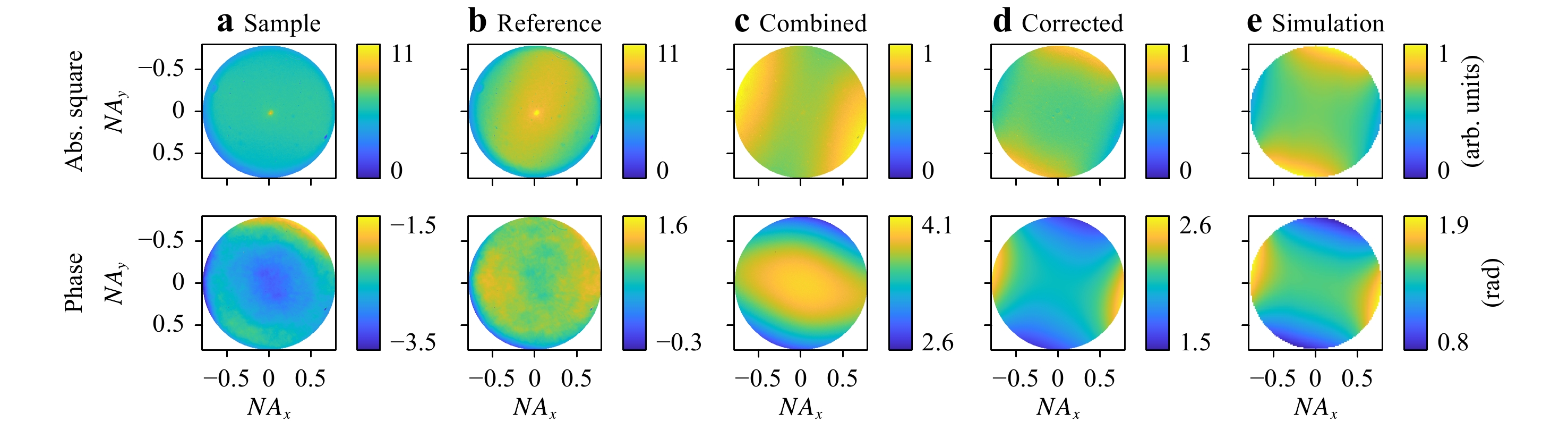
Fig. 6 Step-wise illustration of the calibration procedure.
a Fourier-transformed intensity at an arbitrarily selected wavelength of 628.1 nm, measured on an exemplary silicon line grating; b corresponding reference data obtained on a plane silicon wafer; c result of the combination of both measurements according to Eq. 4; d final result after additional corrections; e corresponding simulation results for comparison.For comparison, the absolute square and phase were also simulated using the nominal grating parameters as determined by additional SEM measurements (see Table 1). The corresponding results are presented in Fig. 6e. Except for a global offset in phase, the calibrated measurements coincide well with the simulations. This statement holds true even for the largest NA values, which implies that the setup imperfections (including the performance of the microscope objectives and beam splitters) are very well corrected. It should be noted that the mentioned phase offset does not influence the Mueller matrix as long as it is the same throughout the entire measurement set. The RMS between the measurement and simulation amounts to 5.0% in the case of the absolute square and 5.2% in the case of the phase, provided that the mean value is subtracted from each phase distribution before relating them to each other. The RMS values are slightly larger than those obtained during the pure intensity measurements shown in Fig. 4, but this was to be expected because the measurement procedure requires additional steps and is hence more complex and error-prone. In addition, the target modelling is more elaborate.
Parameter SEM AFM Scatterometry Top-cd (nm) 51.2 ± 2.9 − 51 Height (nm) 70.1 ± 3.7 70.9 ± 1.1 70 Sidewall angle (°) 77.5 ± 5.3 − 81 Table 1. Parameter values of the silicon line grating obtained directly from SEM and AFM measurements, and indirectly from scatterometric measurements via model-based reconstruction. The specified uncertainties are the standard deviations obtained from averaging over ten measurement sites per parameter. In AFM measurements, lateral dimensions and sidewall shapes are always affected by the tip shape, which is why we omitted the corresponding values.
-
The determination of the Jones matrix
$ J $ of the sample requires four measurements with different angular positions of the polariser and analyser. Angles$ {\theta }_{P} $ and$ {\theta }_{A} $ are defined relative to the orientation of a line-grating target: 0° (90°) corresponds to a polarising or analysing direction perpendicular (parallel) to the grating lines in the Fourier plane of the microscope objective. Because the grating lines are oriented along the$ y $ -axis (see Fig. 1), 0° (90°) is denoted by the subscript$ x $ ($ y $ ).The most obvious choice of angle combinations
$ \left({\theta }_{P},{\theta }_{A}\right) $ is (0°, 0°), (0°, 90°), (90°, 0°), and (90°, 90°). However, the second and third settings with crossed polariser and analyser lead to sharp phase jumps of$ \mathrm{\pi } $ from quadrant to quadrant in the Fourier-plane phase distribution, which is problematic from an experimental point of view. The transitions are typically smeared out in the measurement, thus complicating the calibration and especially phase correction. Therefore, we changed both polariser directions by 30° while maintaining the analyser directions. All of the resulting combinations (30°, 0°), (30°, 90°), (120°, 0°), and (120°, 90°) generate smooth intensity and phase distributions in the Fourier plane. In the same order, the corresponding measurement results are denoted as$ {E}_{x}^{\left(1\right)} $ ,$ {E}_{y}^{\left(1\right)} $ ,$ {E}_{x}^{\left(2\right)} $ , and$ {E}_{y}^{\left(2\right)} $ . We want to emphasise that this specific choice of angle is arbitrary at the moment. Other angles would have been possible as well, and it might be beneficial to optimise the angular settings as a function of the target in the future.For the calculation of the Jones matrix, the measurement results are transferred from the
$ x $ -$ y $ to a$ p $ -$ s $ coordinate system via$$ \left(\begin{array}{c}{E}_{p}^{\left(j\right)}\\ {E}_{s}^{\left(j\right)}\end{array}\right)=\left(\begin{array}{cc}\mathrm{cos}\varphi & \mathrm{sin}\varphi \\ -\mathrm{sin}\varphi & \mathrm{cos}\varphi \end{array}\right) \cdot \left(\begin{array}{c}{E}_{x}^{\left(j\right)}\\ {E}_{y}^{\left(j\right)}\end{array}\right) $$ (7) where the index
$ j\in \left\{\mathrm{1,2}\right\} $ represents the two polariser angles$ {\theta }_{P}^{\left(j\right)} $ and$ \varphi $ is the azimuth angle in the Fourier plane, as shown in Fig. 3a. The Jones matrix$ J $ of the sample relates the initial polarisation state of the illumination to the results of Eq. 7:$$ \left(\begin{array}{cc}{E}_{p}^{\left(1\right)}& {E}_{p}^{\left(2\right)}\\ {E}_{s}^{\left(1\right)}& {E}_{s}^{\left(2\right)}\end{array}\right)=J \cdot \left(\begin{array}{cc}{E}_{p,\mathrm{i}\mathrm{n}}^{\left(1\right)}& {E}_{p,\mathrm{i}\mathrm{n}}^{\left(2\right)}\\ {E}_{s,\mathrm{i}\mathrm{n}}^{\left(1\right)}& {E}_{s,\mathrm{i}\mathrm{n}}^{\left(2\right)}\end{array}\right) $$ (8) with
$$ \left(\begin{array}{c}{E}_{p,\mathrm{i}\mathrm{n}}^{\left(j\right)}\\ {E}_{s,\mathrm{i}\mathrm{n}}^{\left(j\right)}\end{array}\right)=\left(\begin{array}{cc}\mathrm{cos}\varphi & \mathrm{sin}\varphi \\ -\mathrm{sin}\varphi & \mathrm{cos}\varphi \end{array}\right) \cdot \left(\begin{array}{c}\mathrm{cos}{\theta }_{P}^{\left(j\right)}\\ \mathrm{sin}{\theta }_{P}^{\left(j\right)}\end{array}\right) $$ (9) By inversion of the illumination matrix on the right-hand side of Eq. 8, the Jones matrix is calculated as follows:
$$ J=\left(\begin{array}{cc}{E}_{p}^{\left(1\right)}& {E}_{p}^{\left(2\right)}\\ {E}_{s}^{\left(1\right)}& {E}_{s}^{\left(2\right)}\end{array}\right) \cdot {\left(\begin{array}{cc}{E}_{p,\mathrm{i}\mathrm{n}}^{\left(1\right)}& {E}_{p,\mathrm{i}\mathrm{n}}^{\left(2\right)}\\ {E}_{s,\mathrm{i}\mathrm{n}}^{\left(1\right)}& {E}_{s,\mathrm{i}\mathrm{n}}^{\left(2\right)}\end{array}\right)}^{-1} $$ (10) Clearly, the determinant of the illumination matrix must be different from zero for this step, but this can easily be assured by the choice of polariser angles. We want to emphasise again that the correct relative phase relationships between all four measurements are guaranteed by the sensor calibration. The global phase remains unknown, but a common offset does not change the Mueller matrix M. Using the result from Eq. 10, M follows from20
$$ M=\left(\begin{array}{cccc}{m}_{11}& {m}_{12}& {m}_{13}& {m}_{14}\\ {m}_{21}& {m}_{22}& {m}_{23}& {m}_{24}\\ {m}_{31}& {m}_{32}& {m}_{33}& {m}_{34}\\ {m}_{41}& {m}_{42}& {m}_{43}& {m}_{44}\end{array}\right)=A\left(J\otimes {J}^{*}\right){A}^{-1} $$ (11) where
$ {J}^{*} $ denotes the complex conjugate of$ J $ ,$ \otimes $ is the Kronecker tensor product, and matrix A is defined as$$ A=\left(\begin{array}{cccc}1& 0& 0& 1\\ 1& 0& 0& -1\\ 0& 1& 1& 0\\ 0& -\mathrm{i}& \mathrm{i}& 0\end{array}\right) $$ (12) Because our setup is not capable of measuring absolute intensities, we normalise all Mueller matrices to their respective first element,
$ {m}_{11} $ . It should also be noted that all Mueller matrices are depicted in a$ p $ -$ s $ coordinate system, whereas the intensity and phase distributions shown in Figs. 1, 4, and 6 are displayed in the laboratory$ x $ -$ y $ coordinate system. We could have transformed the Mueller matrices to the$ x $ -$ y $ coordinate system as well, but this additional step is unnecessary for model-based reconstruction. Finally, it is important to keep in mind that we assumed the optical system and the sample to be non-depolarising. Consequently, Mueller matrix M from Eq. 11 is actually a Mueller-Jones matrix with only seven independent elements20. -
The basic idea of scatterometry – finding the theoretical object whose response coincides with the measured one – requires a constant comparison between simulation and measurement. We employ the rigorous coupled-wave analysis21−23 (RCWA) theory for the simulation of the light-structure interaction. Our in-house-developed software package ITO MicroSim24−26 includes state-of-the-art RCWA algorithms and models the full microscopic image formation.
The Fourier plane of the microscope objective is sampled by an equidistant grid in
$ x $ - and$ y $ -directions, as shown in Fig. 3a. Each grid element$ \left({NA}_{x},{NA}_{y}\right) $ corresponds to a plane wave propagating in a certain direction, which is specified in terms of the azimuth angle$ \varphi $ and the angle of incidence$ \alpha $ , as shown in Fig. 3b. For each angle combination, illumination wavelength, and initial state of polarisation, one simulation is performed, providing the$ x $ - and$ y $ -component of the electric field in the back-focal plane. For the calculation of the Jones and Mueller matrices, the resulting phase angles are modified according to Eq. 5, and two simulations at the selected polariser angles$ {\theta }_{P}^{\left(j\right)} $ are combined according to Eqs. 7 to 12. This procedure is repeated for all relevant angles and wavelengths to build the Fourier plane images. Note that for the analysis of isotropic samples such as the unstructured silicon wafer, the RCWA would not have been necessary, but we still used it to make all results directly comparable.Our first test target is a dense silicon (Si) line grating with a pitch Λ of 150 nm. Fig. 7 shows a schematic drawing of the grating profile. The silicon mid-cd (measured at half of the grating line height
$ h $ ) remains constant for all sidewall angles σ. A native silicon-dioxide (SiO2) layer with a thickness$ d $ of 3 nm homogeneously covers the entire grating. The refractive indices are taken from the literature27. It should be noted that the top and bottom roundings, as well as the line edge roughness, are not considered here, but will be included in future work. To model the tilted sidewalls in the RCWA, it is necessary to divide the structure into layers in the$ z $ -direction. The number of layers and the number of harmonics are chosen to be sufficiently large to ensure convergence of the simulation results for typical parameter variations.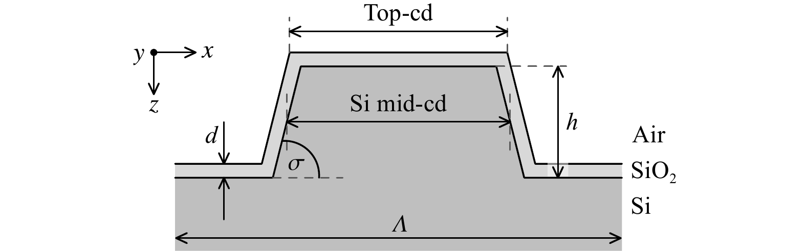
Fig. 7 Grating model.
Schematic of the silicon line-grating profile (not to scale). The top-cd, as determined in SEM measurements, includes the oxide (SiO2) layer, whereas in the simulations, we define the line width via the pure silicon (Si) mid-cd. -
As already mentioned, our first test target for model-based feature reconstruction is a dense silicon line grating with a pitch of 150 nm. Considering that our sensor operates in the visible range of the spectrum, this structure is already in the sub-wavelength regime. Fig. 8 shows an SEM cross-sectional image of the grating. Note that the tilt angle of the stage (51.3°) causes perspective distortion and makes the line height appear smaller than it really is. The total target area is 200 × 200 µm2, and we employed a field stop to limit the diameter of the illumination spot to approximately 70 µm.
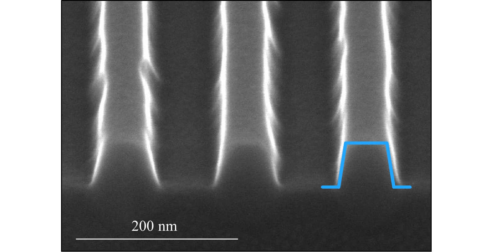
Fig. 8 SEM cross-sectional image of the silicon line grating.
The measurement was performed on an FEI Helios NanoLab 600. The blue grating profile illustrates the reconstructed parameter values. Note that the profile is compressed in its height according to the tilt angle of the stage.The measured Mueller matrices are shown in Figs. 9a, 10a. In Fig. 9a, the wavelength is fixed at an exemplary value of 546.4 nm, and all matrix elements at all angles are displayed simultaneously at this single wavelength. The wavelength dependence can then be assessed from Fig. 10a, where only the Mueller matrix element
$ {m}_{13} $ at all angles is shown at several wavelengths in the range 520–680 nm. The selection of the matrix element and the wavelengths in the specified range are arbitrary and simply made to reduce the amount of data for the plots. Note that all matrix elements are normalised to the first element,$ {m}_{11} $ . Outside of the wavelength range mentioned previously, the light intensity is relatively low (see Fig. 4b). Consequently, we are faced with poor signal-to-noise ratios in these regions, but this limitation could, in principle, be overcome by switching to a different light source.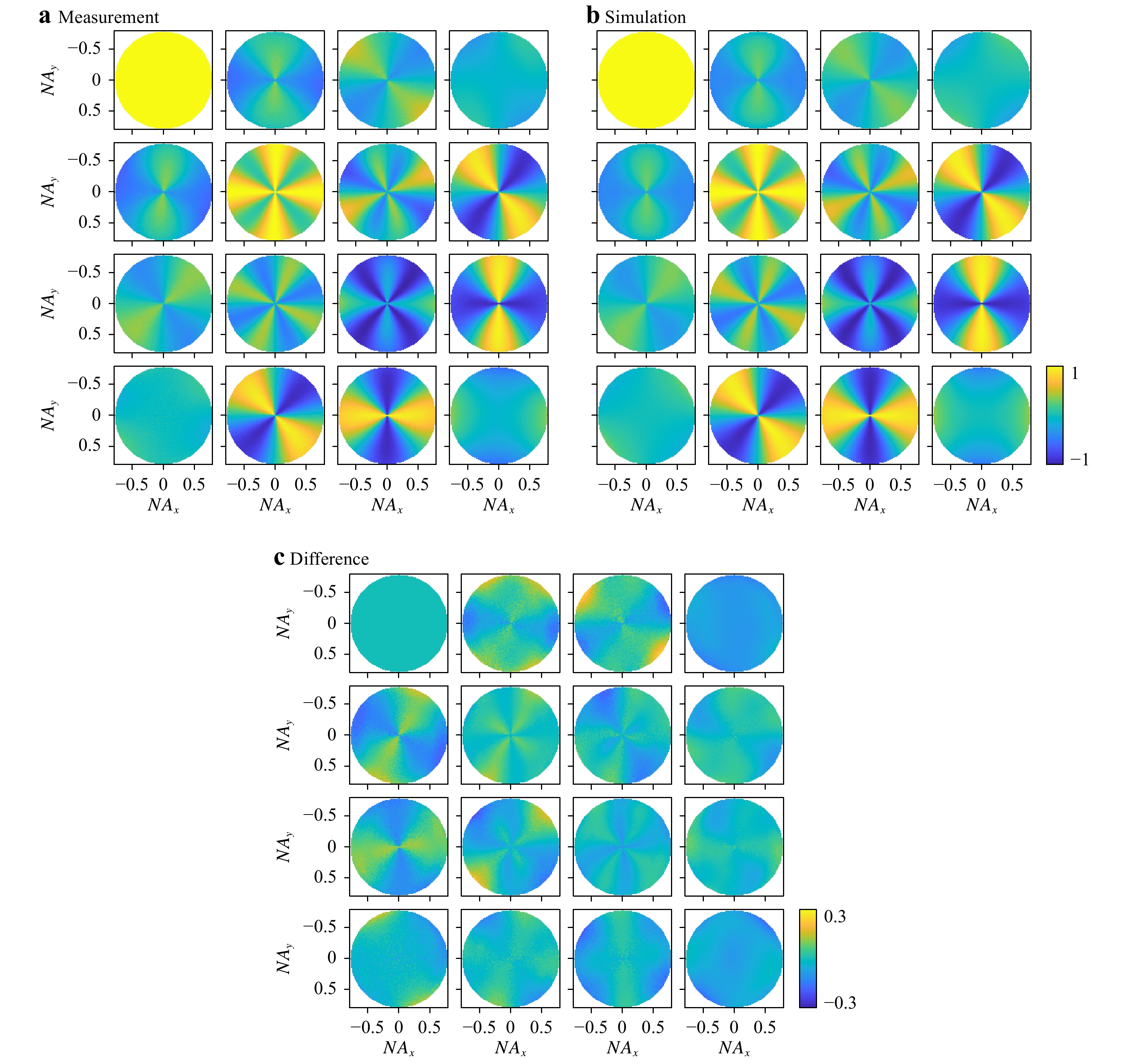
Fig. 9 Mueller matrix, all 16 matrix elements at all angles, but at a single wavelength only (546.4 nm).
a Measurement; b simulation using the optimum set of parameter values obtained from the model-based reconstruction; c difference between measurement and simulation. Note the rescaled colour bar in c.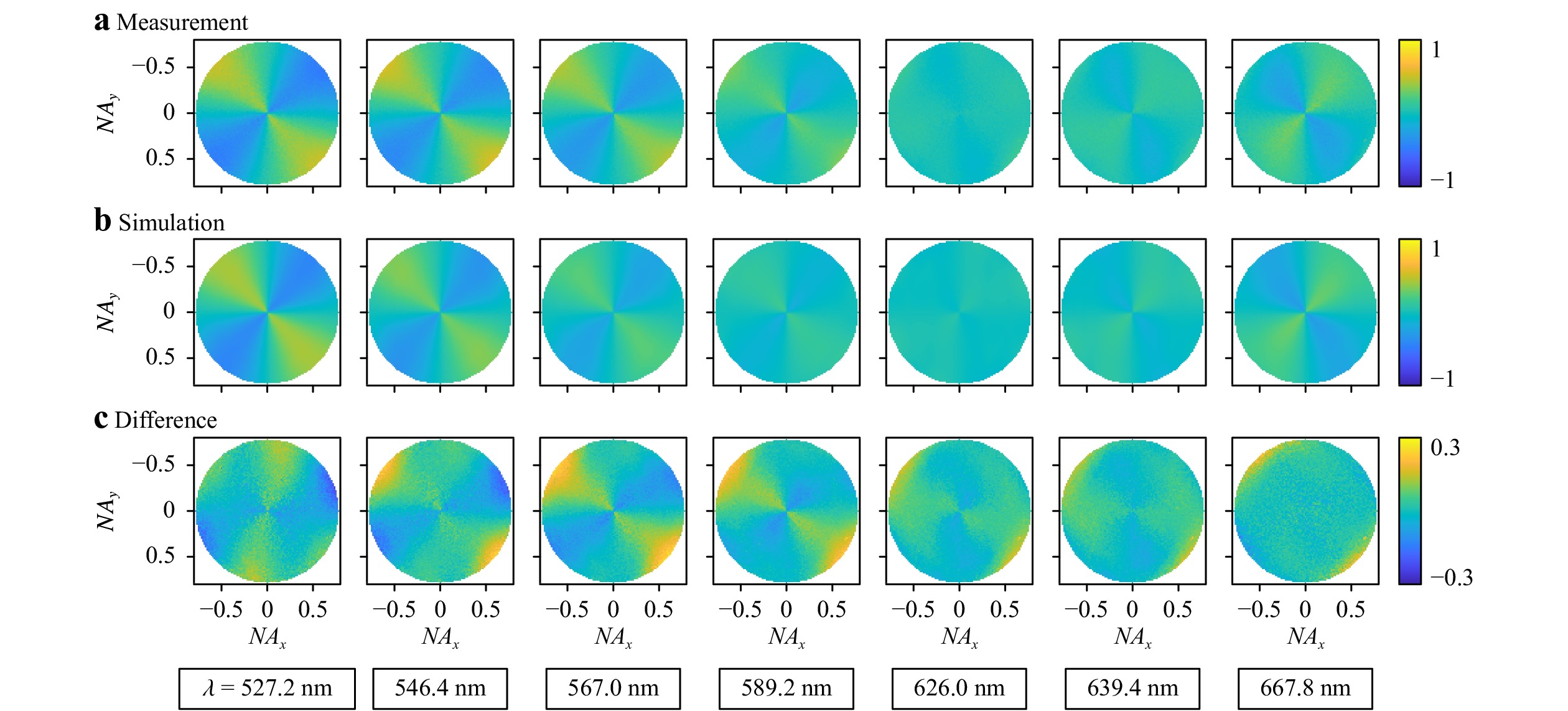
Fig. 10 Mueller-matrix element
$ {\mathit{m}}_{13} $ at all angles and at different wavelengths.a Measurement; b simulation; c difference between measurement and simulation. Again, note the rescaled colour bar in c.The scan of the reference arm was performed with a step size of 25 nm, and a total of 600 images were recorded. This parameter combination corresponds to a scan length of 15.0 µm, which enables the measurement of 14 wavelengths in the desired range. From additional simulations, this value is known to be sufficient in most cases to achieve convergence of the associated parameter uncertainties.
To retrieve the grating parameters, we compare the measured Mueller matrices to a library of simulated ones2. For library generation, all grating parameters are varied around their nominal values, and the corresponding Mueller matrices are calculated at all relevant wavelengths and angles. We determined the nominal values of the silicon line grating by performing additional measurements using a scanning electron microscope (SEM) and an atomic force microscope (AFM).
The SEM image shown in Fig. 8 suggests that the grating profile can be described well by three parameters: the line width (or critical dimension cd) at the top of the line, the line’s height, and the sidewall angle; see also Fig. 7. Clearly, the lines feature a certain roughness, and the parameter values are expected to vary from measurement site to site. Because our scatterometric approach averages over many grating lines at once, we also averaged the SEM and AFM measurement values over ten positions per parameter. The corresponding mean values and their standard deviations are summarised in the second and third columns of Table 1.
The standard deviations listed in Table 1 are mainly caused by the variation of the grating parameters over the target area, and partly by the user influence occurring during the cursor placement in a measurement. Additionally, both AFM and SEM may feature systematic calibration uncertainties that are not considered in Table 1. Although the good agreement between the measured height values suggests that the systematic errors are insignificant, we will still discuss the AFM and SEM calibration at the end of this section.
In our simulations, the width of the grating line is defined by the silicon mid-cd (at half of the grating line’s height) without the oxide layer, as shown in Fig. 7. With the mean SEM values from Table 1 and a constant oxide thickness of 3 nm, a silicon mid-cd of approximately 62 nm is obtained. For the computation of the library, we vary the silicon mid-cd by 20 nm around this value, that is, between 52 and 72 nm in steps of 1 nm. The line’s height is varied between 60 and 80 nm, also in steps of 1 nm, and the sidewall angle between 73 and 86° in steps of 1°. The top and bottom roundings, as well as the line edge roughness, are not considered here. The library is then compared to the measurement, and for each combination
$ \overrightarrow{p} $ of parameter values, the differences between the measurement and simulation are quantified by calculating the RMS:$${\rm{RMS}}\left( {\vec p} \right) = \frac{1}{{15 \cdot L}}\mathop \sum \nolimits_{l = 1}^L \underbrace {\mathop \sum \nolimits_{i = 1}^4 \mathop \sum \nolimits_{j = 1}^4 \sqrt {\frac{{\displaystyle\mathop \sum \nolimits_{k = 1}^K {{\left[ {m_{ij}^{{\rm{meas}}}\left( {k,l} \right) - m_{ij}^{{\rm{sim}}}\left( {k,l,\vec p} \right)} \right]}^2}}}{K}} }_{\left( {\neg \;i = j = 1} \right)}$$ (13) In Eq. 13,
$ {m}_{ij}^{\mathrm{m}\mathrm{e}\mathrm{a}\mathrm{s}} $ ($ {m}_{ij}^{\mathrm{s}\mathrm{i}\mathrm{m}} $ ) is the measured (simulated) Mueller-matrix element$ {m}_{ij} $ at the wavelength index$ l $ and angle index$ k $ . L is the total number of wavelengths, and K is the total number of angles, that is, the number of NA coordinates$ \left({NA}_{x},{NA}_{y}\right) $ within the accessible maximum NA of 0.8. The Mueller-matrix element$ {m}_{11} $ is omitted because it is used to normalise all elements and is, hence, always equal to one.For the reconstruction of the silicon line grating, we consider L = 14 wavelengths and K = 1257 NA coordinates. The value of K corresponds to a 41 × 41 grid in the Fourier plane. Our measurements offer a considerably higher angular resolution, but we still limited the number of pixels to reduce the computational effort required for library generation. Within the analysed parameter ranges, the largest RMS value is 26.2%, whereas the smallest is 8.2%. The minimum RMS value defines the best match, and hence, the optimum parameter set
$ \overrightarrow{p} $ , whose values represent the theoretical grating profile coming closest to the real one. The optimum parameter values are listed in the fourth column of Table 1. Note that to simplify the comparison, the silicon mid-cd was re-converted to the total top-cd, including the oxide layer. The corresponding simulation results are depicted in Figs. 9b, 10b, and the remaining differences between the measurement and simulation can be assessed from Figs. 9c, 10c. All results are discussed in Section 6. -
The SEM was calibrated on a waffle-pattern diffraction grating featuring 2160 lines per mm, which corresponds to a pitch of approximately 463 nm (magnification calibration target no. 607 from Ted Pella, Redding, CA, USA). The line width uncertainty amounts to ± 10 nm, but the corresponding calibration error decreases with the feature size of the device under test.
The calibration of the AFM was verified using fused-silica reference-artefact structures on a silicon substrate (target HS-100MG from BudgetSensors, Sofia, Bulgaria). To reduce sample-induced measurement errors, the sample was overcoated with chromium (75 nm). The sample features binary step structures with a nominal height of 113 nm ± 3%, as calibrated by the vendor. The lateral dimensions vary from 5 to 30 µm. With the overcoating, the sample is well suited for AFM probes as well as optical probes. The sample was calibrated on the nanopositioning and nanomeasuring machine NPMM-200 (ref. 28) using an optical fixed-focus probe. The NPMM-200 employs six interferometers with a five-axis stage control to implement an extended Abbe principle in three axes, allowing for high-accuracy height measurements down to sub-0.1-nm repeatability even for large step heights. The measured height of the sample is 113.70 nm and the standard deviation of 10 measurements amounts to 0.15 nm. The measurement uncertainty is dominated by the sample nanotopography and is estimated from measurements at different positions to be better than ± 1 nm. In summary, the agreement between the vendor specification and NPMM-200 measurement results is excellent.
In addition to this successful cross-check with the NPMM-200, it should be emphasised again that the height values measured with the SEM and AFM coincide well (see Table 1). Therefore, we are convinced that, at least for our specific application, the systematic calibration error per technique is small enough to enable reliable quantitative comparisons between the two techniques, and even more important, with our scatterometric results.
-
The quality of our model-based feature reconstruction can be assessed from the match between the measured and simulated signatures and the consistency of the results obtained using different measurement tools.
Figs. 9 and 10 demonstrate that our measurements agree very well with the simulations: the theoretically expected angle and wavelength dependence are correctly reproduced for all Mueller-matrix elements. Note, for example, that the structure in the matrix element
$ {m}_{13} $ shown in Fig. 10 gradually disappears with increasing wavelength, and reappears with reversed angular dependence in the expected wavelength range. In comparison to the test measurements on the plane silicon wafer, however, the RMS increased from 1.6% (2.3%) to 8.2%. The larger deviations can be attributed to multiple factors: First, the full white-light signal was considered in the case of the plane silicon wafer, whereas in the case of the silicon line grating, the wavelengths were separated by Fourier spectroscopy. Second, the measurement on the plane silicon wafer was performed without the reference arm, that is, without retrieving phase information, whereas the determination of the Mueller matrix requires phase information from as many as four measurements with correct relative phase relationships. Naturally, both of the extra measurement steps introduce additional errors. Third, the simulation of the intensity response from the plane silicon wafer is considerably less demanding than the accurate modelling of the silicon line grating. Based on the best-fit parameters, we inserted a true-to-scale sketch of the reconstructed grating profile into the SEM image shown in Fig. 8. Although the real profile and the sketched one already agree well, it is likely that the match and the RMS value could be improved further by taking more grating parameters into account.Table 1 compares the SEM, AFM, and scatterometric measurements. The match is excellent: all parameter values determined indirectly by scatterometry lie within the uncertainty budgets of the other two direct methods, which implies that any systematic error must be insignificant. Of all three parameters, the difference between the values is largest for the sidewall angle, but we already know from the SEM measurements that this is the parameter most prone to heavy variations over the target area (see Table 1). It is, therefore, understandable that averaging over ten SEM measurements taken at different localised measurement sites produces a slightly different result than the continuous optical averaging over hundreds of grating lines illuminated by the 70-µm spot.
In summary, the successful model-based feature reconstruction of the silicon line grating validates the practical feasibility of the proposed scatterometric sensor concept. The RMS value of 8.2% implies that there is still some room for improvement, but the overall performance and the tool matching are already promising.
When comparing our sensor to other state-of-the-art scatterometers, it is also important to consider computational effort. Generally, if the sensor provides a higher information content, more simulations are required for comparison. In the case of complex targets with many parameters and a large range of illumination wavelengths and angles, the computation time for a complete library with all parameter combinations may become immense. As mentioned in the introduction, however, it is often advantageous to adapt the measurement data range used as input for the reconstruction to the specific target under test. Besides increasing the sensitivity and robustness, this approach helps to reduce the computational effort. The determination of the optimum data subset per target requires experience with similar targets or a preceding sensitivity analysis; nonetheless, we are optimistic that the extra effort is justified by the improved reconstruction results. Instead of a straightforward library search, it might also be beneficial to implement a more time-efficient optimisation routine, such as the Levenberg-Marquardt regression29.
Currently, we are developing the concept further into various directions: First, we repeat the analysis of the silicon line grating with an enlarged parameter space. Starting from the top and bottom roundings, we plan to include line-edge roughness30 and reconstruct the refractive indices of the involved materials. Second, we perform short- and long-term reproducibility tests. Subsequently, we plan to analyse the sensor’s sensitivity towards deep sub-wavelength features by methodically decreasing the pitch and cd values of the grating. Based on the results of our simulation study15, we also expect excellent sensitivity towards target asymmetry. We plan to test the corresponding performance by analysing line gratings structured by double patterning with controlled overlay variation.
Depending on the desired wavelength resolution, recording a full set of four measurements takes approximately 5-10 min. In terms of throughput and stability, it would be advantageous to reduce the acquisition time. This can, in principle, be achieved by increasing the scan speed of the reference arm or by decreasing the required number of measurements. While the first approach is mainly an engineering task, the second is scientifically more demanding. As a long-term goal, we are planning to reduce the number of measurements from four to two by integrating a photoelastic modulator (PEM) into the Koehler illumination arm. Instead of performing single-shot intensity measurements at each scan position of the reference arm, it then becomes necessary to record time-resolved signals. Owing to the high modulation frequency of the PEM in the kHz range, we will have to replace the standard Fourier-plane camera with a dedicated high-speed camera. Once this setup is fully functional, a second PEM with a different modulation frequency may be integrated into the detection arm to reduce the number of measurements from two to one. We will report the corresponding results in a follow-up publication.
-
This work was supported by the Deutsche Forschungsgemeinschaft (DFG, German Research Foundation) under grant number Os 111/50-1. We thank Martina Zach and Michael Haub for performing AFM and SEM measurements, respectively. Furthermore, we thank the DFG for supporting the acquisition of the NPMM-200 under the grant number Os 111/44-1, and we thank Christian Schober and Christof Pruß for carrying out the measurements on the NPMM-200.
Model-based characterisation of complex periodic nanostructures by white-light Mueller-matrix Fourier scatterometry
- Light: Advanced Manufacturing 2, Article number: 18 (2021)
- Received: 22 January 2021
- Revised: 26 May 2021
- Accepted: 26 May 2021 Published online: 23 June 2021
doi: https://doi.org/10.37188/lam.2021.018
Abstract: Optical scatterometry is one of the most important metrology techniques for process monitoring in high-volume semiconductor manufacturing. By comparing measured signatures to modelled ones, scatterometry indirectly retrieves the dimensions of nanostructures and, hence, solves an inverse problem. However, the increasing design complexity of modern semiconductor devices makes modelling of the structures ever more difficult and requires a multitude of parameters. Such large parameter spaces typically cause ambiguities in the reconstruction process, thereby complicating the solution of the inherently ill-posed inverse problem further. An effective means of regularisation consists of systematically maximising the information content provided by the optical sensor. With this in mind, we combined the classical techniques of white-light interferometry, Mueller polarimetry, and Fourier scatterometry into one apparatus, allowing for the acquisition of fully angle- and wavelength-resolved Mueller matrices. The large amount of uncorrelated measurement data improve the robustness of the reconstruction in the case of complex multi-parameter problems by increasing the overall sensitivity and reducing cross-correlations. In this study, we discuss the sensor concept and introduce the measurement strategy, calibration routine, and numerical post-processing steps. We verify the practical feasibility of our method by reconstructing the profile parameters of a sub-wavelength silicon line grating. All necessary simulations are based on the rigorous coupled-wave analysis method. Additional measurements performed using a scanning electron microscope and an atomic force microscope confirm the accuracy of the reconstruction results, and hence, the real-world applicability of the proposed sensor concept.
Research Summary
Scatterometry: Novel sensor facilitates the model-based reconstruction of complex nanostructures
With the structure dimensions on modern semiconductor chips having reached the nanometre scale and circuit designs becoming increasingly complex, process monitoring is facing veritable challenges. Optical scatterometry retrieves the parameter values of a nanostructure indirectly by comparing between measured and modelled signatures. However, modelling complex structures requires large parameter spaces, which are known to cause large measurement uncertainties. Maria Laura Gödecke from Germany’s University of Stuttgart and colleagues now report the development of a novel scatterometric sensor that makes full use of the rich polarisation information contained in the angle- and wavelength-resolved Mueller matrix of a nanostructure. Compared to other scatterometric sensors, the information gain improves the sensitivity and robustness of the method. The team verified the practical feasibility of the proposed concept by reconstructing the profile parameters of a sub-wavelength silicon line grating.


Rights and permissions
Open Access This article is licensed under a Creative Commons Attribution 4.0 International License, which permits use, sharing, adaptation, distribution and reproduction in any medium or format, as long as you give appropriate credit to the original author(s) and the source, provide a link to the Creative Commons license, and indicate if changes were made. The images or other third party material in this article are included in the article′s Creative Commons license, unless indicated otherwise in a credit line to the material. If material is not included in the article′s Creative Commons license and your intended use is not permitted by statutory regulation or exceeds the permitted use, you will need to obtain permission directly from the copyright holder. To view a copy of this license, visit http://creativecommons.org/licenses/by/4.0/.

 DownLoad: