


-
Electromagnetically induced transparency (EIT) is a quantum interference phenomenon that exists in coherently driven three-level atomic systems1, 2 and results in the narrow-band cancellation of absorption in the material. A fascinating property of an EIT medium is its ability to significantly reduce the group velocity of light propagating through a material3, thereby enabling EIT-based optical memories and buffering4−6. By mimicking the resonant quantum transitions in an atomic medium, an EIT-like response can be realised in various solid-state systems, including electric circuits7, coupled optical resonators8, 9, and plasmonic metamaterials10−13. Compared with EIT in atomic systems, such analogues can avoid complicated experimental setups required for laser stability and low-temperature environment14, 15. Recently, an EIT analogue using Mie-resonant all-dielectric metasurfaces for engineering light fields with high efficiency has been reported. Such all-dielectric metasurfaces composed of arrays of nanostructured high-refractive-index media simultaneously produce intense electric and magnetic resonances16, 17. In particular, all-dielectric EIT metasurfaces based on a high-index medium such as silicon stripes18, oligomer antennae19, and asymmetric cut-wire meta-atoms20, 21 have been demonstrated recently in the near-infrared (N-IR) region. It is highly desirable to dynamically manipulate the optical characteristics of meta-devices via external control parameters22. All-dielectric metasurfaces that derive their functionality from the intense localised electric and magnetic Mie resonances of a high-index resonator is particularly suitable for achieving this active tunability23−25, owing to their optical resonances, which can be engineered on-demand via metasurface design26. Although researchers have recently investigated different designs of actively tunable all-dielectric metasurfaces, such as the hybridisation of a Si metasurface with a liquid crystal matrix26, 27, paired photon absorptance on Si metasurfaces28, 29, and control of the refractive index via photoexcitation30, the dynamically reversible tuning of all-dielectric metasurfaces remains an under-explored field. Hence, all-dielectric metasurfaces, in which ultrafast and reconfigurable control can be realised, should be fabricated. Moreover, the compatibility of current EIT dielectric metasurfaces with ultrafast photonic systems operating with nanosecond pulses and low-power optically modulated switchers remains a formidable challenge.
Chalcogenide phase change materials (PCMs), such as Ge, Sb, and Te, can be repeatedly (up to 1015 cycles) and promptly (nanoseconds)31 transited between disordered-amorphous and ordered-crystalline states (and even between intermediate states) via appropriate electrical, thermal, or optical stimuli32. Chalcogenide PCMs have been widely applied in electrical memory technologies33. Their optical dielectric constants between the amorphous and crystalline states differ significantly34, 35, rendering them appealing for forming rapid, low-power consumption tunable optical devices36, 37. Recently, Ge–Sb–Te (GST)-based PCMs have garnered significant in the development of active plasmonic meta-devices38−46, which deliver various switchable optical functionalities through integration with metal nanostructures, including tunable perfect absorption47, 48, reconfigurable optical activities41, and multispectral imaging49, 50. Owing to the high refractive index and prominent contrast between structural states within GST, it has recently emerged as a promising paradigm for tunable all-dielectric metasurfaces51−56. However, reverse crystalline-to-amorphous state transitions have not been experimentally realised in most GST dielectric metasurfaces51, 54−56. A few metasurface designs are based on a hybrid of multilayer resonators53, 56, which render them complicated to fabricate, and some of them have polarisation-dependent optical responses51, 54. It is noteworthy that dielectric metasurfaces based on patterned monolithic GST-only films for achieving the dynamic and reversible tuning of an EIT-like response have not yet been realised experimentally.
In this study, we demonstrate the reversible tuning of EIT-like spectra using a GST all-dielectric metasurface possessing magnetic and electric resonances in the N-IR region. The EIT-like resonance was created by coupling between the electric dipolar (ED) and toroidal dipolar (TD) modes52 and can be optically engineered by changing the complex refractive index (nGST) of GST via its phase transition between amorphous and crystalline states. The all-dielectric metasurface comprised round nanohole arrays (RNAs) embedded in a SiO2/Ge2Sb2Te5 (GST225) dual-layer on top of a SiO2 substrate, where a 10-nm-thick SiO2 layer was used to protect the GST225 against oxidation. The GST225 exhibited a refractive index whose real part (Re(nGST)) was between 4 and 7.2 over a 1000–2200 nm spectral region; this range is much larger than those of typical N-IR dielectrics such as PbTe, Si, and Ge. We exploited this high Re(nGST) to design the resonant response in dielectric nanohole metasurfaces, which host complex higher-order modes in the N-IR range. We obtained a broad tuning range of 360 nm and a significant relative modulation contrast of 80% at an EIT resonance of λ = 1400 nm by switching the GST225 layer between its amorphous and crystalline phases. To achieve a reconfigurable EIT response, a reversible phase transition of GST225 must be realised. In this study, we reamorphised GST225 using a nanosecond pulsed laser. Finally, we demonstrated that the group delay of the N-IR light can be actively engineered by reversibly switching the state of GST225 between amorphous and crystalline, which provides a practical method for reconfigurable holograms, sensors, and laser beaming devices, while affording advantages of real-time switching, small footprint, simple geometry, and lightweightness.
-
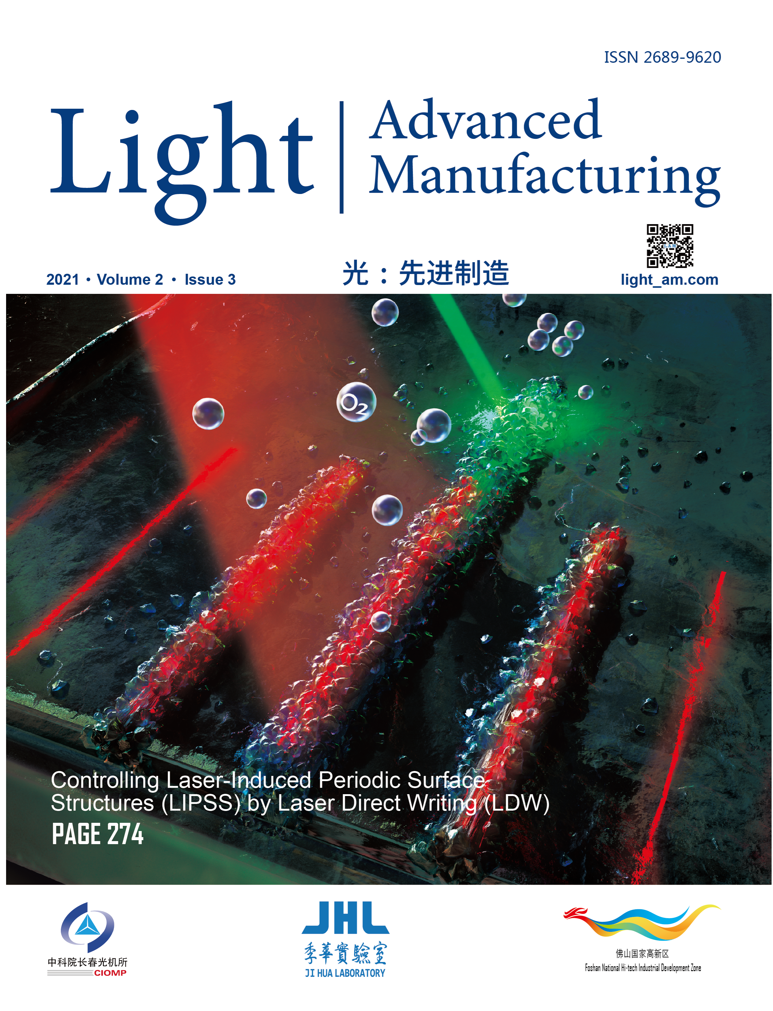
Fig. 1a shows the scheme of our proposed system and the tuning mechanism employed. As a proof-of-concept, we used an all-dielectric metasurface composed of a square array of round nanoholes etched into a SiO2 (10 nm thickness)/GST225(60 nm thickness) dual-layer residing on a SiO2 substrate (Fig. 1a). The top SiO2 layer prevented GST225 from being oxidised. Our proposed all-dielectric EIT metasurface based on GST targets the technologically important N-IR region, which enables highly prominent applications in free-space optical communication and molecular sensing57−61. However, the pitch of the meta-atoms must be much shorter than the resonant wavelength to avoid high-order diffractions. This results in a miniature resonator that is difficult to obtain experimentally in the N-IR regime, such as a square-like ring combined with nanorods54, spheres62, double C-shaped resonators63, cut wires integrated with split-rings64, three cut-outs65, and asymmetric paired rods66. In this study, the nanoholes were used to replace the complicated resonators owing to the ease of fabrication. Such a circular hole array is simple in terms of geometry. The nanohole array design can improve the uniformity of the meta-atoms during fabrication, thereby affording better performing EIT meta-devices. In this study, the GST225 metasurface allows the simultaneous excitation of ED and TD resonances67, where an EIT window can be created via destructive interference between them. The TD moment in the all-dielectric metamaterials is caused by displacement currents (
$\vec{j} $ ), which differs from magnetic resonances in plasmonic metamaterials caused by conduction currents.$ \vec{j} $ assumes the meridian form on the toroidal surface that resembles the poloidal currents and produces a magnetic resonance mode confined within the gedanken torus. Such a configuration can create an electromagnetic analogue of the TD moment in all-dielectric metamaterials68, 69. A schematic illustration of the resonator is shown in Fig. 1b. As shown, the incident wave propagated along the z-direction, and its electric (E-) field polarised along the x-direction. Consequently,$ \vec{j} $ formed two loops of current: clockwise and counterclockwise. These current loops formed a circulated magnetic mode$ \vec{M} $ confined within them. Such a configuration can create a toroidal dipole moment$ \vec{T} $ polarising along the direction of the E-field of the incident light. The interaction between the toroidal dipole$ \vec{T} $ and electric dipole$ \vec{P} $ modes can yield an EIT resonance mode70. Moreover, the interference of strong TD and ED resonances achieved by utilising dielectric resonators enables dynamically and actively reconfigurable EIT meta-devices with high efficiency to be realised. A 60-nm-thick GST225 layer was first deposited on the SiO2 substrate via radio frequency (RF) sputtering from GST225 composition targets. A 10-nm-thick SiO2 film was deposited directly onto the GST225 film. The RNAs were subsequently milled through the SiO2/GST225 dual-layer using a focused ion beam (FIB, FEI Helios NanoLab 600) with a beam current of ≤ 750 pA to prevent the crystallisation of GST225 (through ion beam-caused heating) during milling. A flowchart of the entire fabrication process is schematically illustrated in supplementary Fig. S1. A scanning electron microscopy (SEM) image of the as-deposited (AD) amorphous (AM) GST225 metasurface is shown in the top panel of Fig. 1c. The measured lattice constants and diameters were 890 and 690 nm, respectively, which were similar to the designed values (Fig. 1b). The area of the fabricated metasurface was 300 µm × 300 μm. The cross-sectional SEM image of the metasurface is presented in the bottom panel of Fig. 1c, in which a hole depth of ~70 nm that matches the thickness of the SiO2/GST225 dual-layer is shown. We crystallised the AD-AM GST225 metasurface by thermally annealing it for 30 min at 180 °C on a hot plate in a flowing Ar atmosphere. Fig. 1d shows that the geometries of the RNAs (top panel) and their cross-sections (bottom panel) were well preserved after the structural phase change of GST225 from amorphous to crystalline.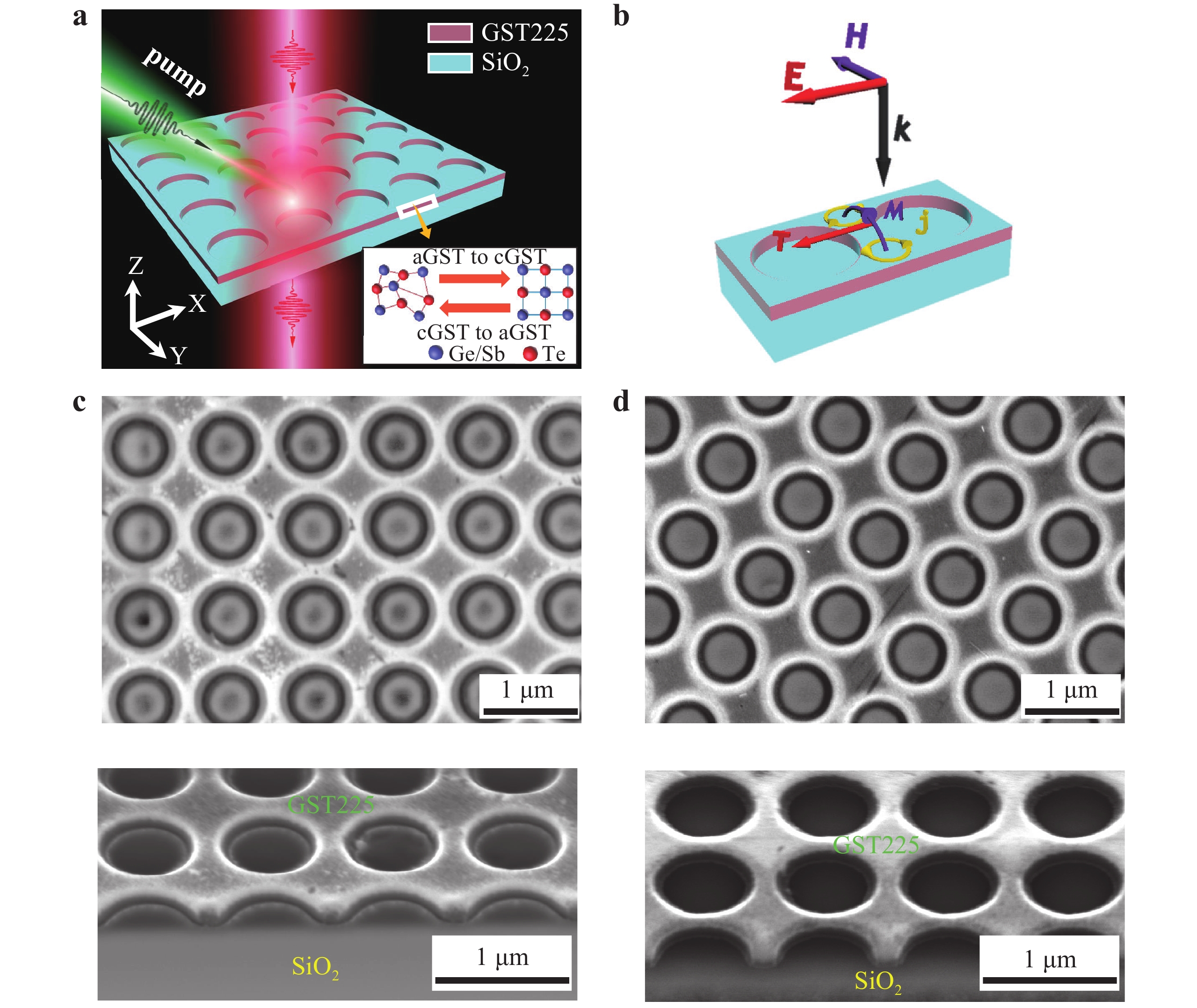
Fig. 1 Configuration of GST225 all-dielectric metasurface.
a Scheme of all-optical, nonvolatile, switchable EIT metasurface, where 1 ns laser pulse reversibly transits GST225 film between amorphous and crystalline states. b Illustration of nanoholes array supplemented with mode and current distribution within each nanohole. Excitation of toroidal dipole moment is demonstrated, where$ \vec{M} $ $ \vec{j} $ $ \vec{T} $ -
In this study, reversible tuning was achieved via the nanosecond pulsed laser beam. The switching relies on two fundamental phase transitions, i.e. amorphisation and recrystallisation, which occur at different temperatures and time scales64. Fig. 2a shows a schematic illustration of the treatment of the GST225 all-dielectric metasurface. First, we crystallised the AD-AM GST225 film by thermally annealing it at 300 °C, which is above the glass-transition temperature TC = 180 °C but below the melting temperature TM = 600 °C, for 30 min on a hot plate in a flowing Ar atmosphere. This process provides a natural switching process that occurs through crystallisation growth and nucleation. Reamorphisation, a melt-quenching process, was achieved by heating GST225 above TM = 600 °C using an ex situ nanosecond laser pulse excitation, followed by rapid cooling32, 71, 72. The nanosecond laser had a peak intensity (fluence) of 430 mWµm−2 with a central wavelength λ = 532 nm, which can yield a numerous electron–hole pairs and melt the GST225. The subsequent fast cooling quenched the melted material into the AM phase (room temperature) at a rate of 109–1010 K/s, which prevents the recrystallisation of the atomic structure68. To recrystallise the melt-quenched (MQ) AM GST225 film, 6 ns laser pulses at λ = 532 nm with a decreasing intensity of 215 mWµm−2 were employed to maintain the GST225 above TC = 180 °C but below TM = 600 °C. This resulted in a significant contrast in the optical properties between the two different structural states, and this phenomenon has been extensively investigated as a platform for efficient, prompt, nonvolatile, reproducible phase changes. Variable-angle spectroscopic ellipsometry (VASE) was used to characterise the optical properties of the 60-nm-thick GST225 layer for the AD-AM (red line), CR (blue line), MQ-AM (orange line), and recrystalline (R-CR, green line) states in the 1000–2200 nm spectral range, from which we extracted the complex refractive index dispersion (Fig. 2b). The Tauc–Lorentz model was used to fit the real (nGST, solid lines) and imaginary (kGST, dashed lines) components of the complex refractive index (NGST = nGST + i × kGST). The nGST changed significantly between the two structural states, resulting in a switchable N-IR resonance that is supported by the RNAs. Overall variations ΔnGST ~ 3.2 and ΔkGST ~ 3.8 were achieved by changing between predominantly covalent bonds in the AM phase and resonant bonds in the CR phase.
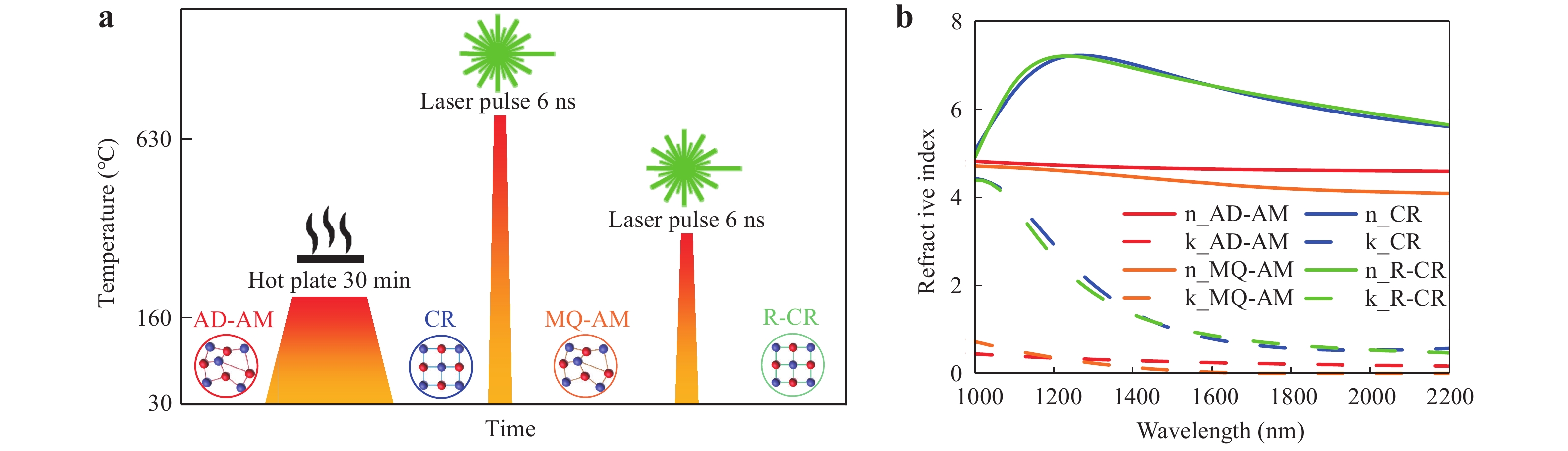
Fig. 2 Treatment for reversible phase change between amorphous and crystalline states.
a Schematic illustration of reversible phase change of GST225 all-dielectric metasurface: AD-AM GST225 was first heated above 180 °C to switch to CR GST225 via hot plate. A 1 ns laser pulse was set to anneal CR GST225 film above 600 °C and reamorphise CR GST225. Subsequent quenching resulted in formation of MQ-AM GST225. To recrystallise MQ-AM GST225, for which a temperature above 180 °C but below 600 °C is required, a 1 ns laser pulse with lower energy was used. b Wavelength-dependent complex refractive index of 60-nm-thick GST225 film at different structural states, i.e. as-deposited amorphous (AD-AM, red line), crystalline (CR, blue line), melt quenched amorphous (MQ-AM, orange line), and recrystalline (R-CR, green line), where refractive index was experimentally measured using VASE over a 1000–2200 nm spectrum (see Methods).The measured transmittance spectra of the fabricated GST225 dielectric metasurface at different structural states are presented in Fig. 3a. The spectra were segregated into two panels to differentiate between the metasurface treatments, where the top panel shows a spectral comparison of the AD-AM (red solid line) to the annealed CR (blue solid line) phases. By contrast, the bottom panel illustrates the spectra comparison of the MQ-AM (orange solid line) to the R-CR (green solid line) states after a nanosecond-laser-enabled phase change. A detailed discussion of the measurement is presented in the Methods section. For the AD-AM and MQ-AM states, a transmittance dip corresponding to the ED resonance occurred at a wavelength of λ1 = 1500 nm. As expected, a second transmittance dip associated with the TD resonance occurred at a shorter wavelength (λ2 = 1220 nm). An EIT peak appeared between two resonance minima with a peak transmittance of 0.5, at a wavelength of λ3 = 1400 nm. The bottom panel shows the transmittance spectra after the crystallisation of GST225 via either thermal heating (CR) or laser transition (R-CR). Here, both the ED and TD Mie-like resonances were suppressed, which obliterated the EIT feature at λ3 = 1400 nm. This is because the crystallisation of GST225 significantly increased kGST, as shown in Fig. 2b. This results in a high contrast ratio and a relative modulation contrast of
$\left| {{T_{AD - AM}} - {T_{CR}}} \right|/{T_{CR}} = 0.8$ at λ3 = 1400 nm, where${T_{AD - AM}}$ and${T_{CR}}$ are the transmissions of the metasurface for the structural states of AD-AM and CR, respectively. Furthermore, the higher nGST of the CR state shifted the resonances to longer wavelengths. The resonant wavelength of the peak transmittance red-shifted from λ3 = 1400 nm to λ4 = 1760 nm upon the thermal annealing of the GST225 dielectric from its AD-AM to CR phase (top panel of Fig. 3a). By contrast, a blue shift of the peak resonance from λ4 = 1760 nm (CR) to λ5 = 1460 nm (MQ-AM) and a red-shift from λ5 = 1460 nm (MQ-AM) to λ6 = 1800 nm (R-CR) were optically realised via the nanosecond pulsed laser. The variations in the resonant frequency imply reversible tuning (λ3→λ4→λ5), which corresponded to the reamorphisation and recrystallisation of the GST225 layer, respectively. The EIT response of the metasurface with an area of 40000 µm2 can switch between two spectrally separate N-IR channels. The active control of the EIT spectra and dynamic band selectivity in the metasurface represent a significant over passive EIT photonic devices.
Fig. 3 Experimental realisation of reconfigurable EIT compared with theory and simulation.
a VASE-measured transmittance spectra, b FDTD-simulated transmittance spectra, and c theoretically fitted transmittance spectra of GST225 all-dielectric metasurface with various structural states, i.e. AD-AM (red line), CR(blue line), MQ-AM (orange line), and R-CR (green line).To compare the measured results with the theoretical predictions, we performed a numerical simulation using the finite difference time domain (FDTD) method to solve Maxwell’s equations for the metasurface73. The simulation data shown in Fig. 3b agree well with the experimental measurements (Fig. 3a). In the model, we employed the VASE-measured refractive index for the GST225 film with different structural states (Fig. 2b) as well as for the geometrical parameters of the metasurface obtained from the SEM images presented in Fig. 1c. The refractive index for the SiO2 substrate was based on Palik74. The transmittance spectra were simulated by illuminating the metasurfaces with a plane wave at normal incidence, as shown in Fig. 1a. A detailed explanation of the model is provided in the Methods section. The reversible tuning of the EIT resonance was numerically observed by altering the structural phase of GST225 between the amorphous and crystalline phases. The profiles of the simulated spectra agreed well with the measurements, although the quality factor of the measurement decreased. A few factors resulted in discrepancies between the simulation and experiment. First, in the ideal model, we did not consider the surface roughness, structural disorder, finite size, and imperfections in the fabricated metasurface (e.g. small over-milling of RNAs into the substrate and stoichiometric variations in the GST225 layer during FIB milling). These aspects can induce additional scattering loss, which consequently decreases the Q-factor and slightly broadens the measured spectra75, 76. Additionally, gallium contamination during FIB milling may introduce absorption and stoichiometrically modify the nanostructured GST (e.g. decreasing the refractive index caused by irradiation, creation of gallium implantation, and defects)77, 78. In the experiment, we measured the transmittance spectra of the metasurface in the far-field. In the model, we calculated the spectra in the near-field of the metasurface that introduced variations between the experiment and simulation79. Herein, we investigate the physical origin of the active modulation of the EIT response and the near-field coupling effect between the ED and TD resonances in the GST225 meta-atom based on a coupled harmonic Lorentz oscillator model13, as follows:
$$ {\omega }_{E}^{-2}\ddot{m}\left(t\right)+{\Pi }_{E}{\omega }_{E}^{-1}\dot{m}\left(t\right)+m\left(t\right)=g\left(t\right)-\kappa n\left(t\right) $$ (1) $$ {\omega }_{M}^{-2}\ddot{n}\left(t\right)+{\Pi }_{M}{\omega }_{M}^{-1}\dot{n}\left(t\right)+n\left(t\right)=-\kappa m\left(t\right) $$ (2) where
${\omega _E}$ ,${\omega _M}$ ,${\Pi _E}$ , and${\Pi _M}$ represent the resonant frequencies and damping rates of the ED and TD resonances, respectively.${\Pi _E}$ and${\Pi _M}$ are expressed by the excitation$n(t)$ and$m(t)$ accordingly, and the external driving force$g(t)$ drives${\Pi _E}$ . The two resonances were linearly coupled with the coupling strength$\kappa $ . Equations (1) and (2) are solved in the frequency domain by assuming solution forms of$ m\left(t\right)=\tilde {m}\left(\omega \right)\mathrm{e}\mathrm{x}\mathrm{p}(-i\omega t) $ and$ n\left(t\right)= $ $ \tilde {n}\left(\omega \right)\mathrm{e}\mathrm{x}\mathrm{p}(-i\omega t) $ , respectively, as follows:$$ \tilde {m}\left(\omega \right)=\frac{{\Delta }_{E}\left(\omega \right)\tilde {g}\left(\omega \right)}{{\Delta }_{E}\left(\omega \right){\Delta }_{M}\left(\omega \right)-{\kappa }^{2}} $$ (3) $$ \tilde {n}\left(\omega \right)=\frac{\kappa \tilde {g}\left(\omega \right)}{{\Delta }_{E}\left(\omega \right){\Delta }_{M}\left(\omega \right)-{\kappa }^{2}} $$ (4) where
${\Delta _{E,M}}(\omega ) = 1 - {(\omega /{\omega _{E,M}})^2} - i{\Pi _{E,M}}(\omega /{\omega _{E,M}})$ . The single resonator of the EIT metasurface can be expressed using an electric current sheet based on the surface conductivity:$$ {\sigma }_{s}={\varepsilon }_{0}{\chi }_{s}^{\left(static\right)}\frac{-i\omega \tilde {m}\left(\omega \right)}{\tilde {g}\left(\omega \right)}=\frac{-i\omega \beta {\Delta }_{M}\left(\omega \right)}{{\Delta }_{M}\left(\omega \right){\Delta }_{E}\left(\omega \right)-{\kappa }^{2}} $$ (5) where
${\chi _s}$ is the surface susceptibility, and$\beta \,{\rm{ = }}\,{\varepsilon _0}\chi _s^{(static)}$ . Therefore, the transmittance coefficient of the EIT metasurface can be expressed as$$T = \frac{2}{{2 + {\eta _0}{\sigma _s}}}$$ (6) where
${\eta _0}$ represents the wave impedance in free space.In Fig. 3c, the measured transmittance spectra of the GST225 metasurface in the amorphous and crystalline states are analytically fitted using Eq. 6; as shown, they agree reasonably well with both the measured (top panel of Fig. 3a) and simulated (Fig. 3b) data. The fitting parameters for,
${\omega _E}$ ,${\omega _M}$ ,${\Pi _E}$ ,${\Pi _M}$ , and$\kappa $ are listed in Table S1 in the Supplementary Information. As shown, the damping rate of the TD mode${\Pi _M}$ increased significantly (i.e. by two orders of magnitude) for the CR state, indicating that the phase transition of GST225 changed the resonant strength of the TD mode. Therefore, the active tuning of the EIT resonance was due to the difference in${\Pi _M}$ . In the AM-GST225 metasurface with a low${\Pi _M}$ , the two pathways interfered destructively to generate a sharp EIT transmittance peak. However, by crystallising the GST225 layer, the loss in the resonator increased, which suppressed the excitation of the TD mode and removed the EIT resonant peak. Such an EIT response can be reversibly activated by reamorphising the metasurface. -
Fig. 3 shows that our proposed GST225 metasurface can realise the dynamic and reversible tuning of the ED and TD resonances, resulting in a reconfigurable EIT response. The fundamental mechanism of such behaviour can be investigated by analysing the mode decomposition and scrutinising the near-field distributions of the metasurface at the ED and TD Mie-type resonances for the different GST225 states. To investigate the nature of the induced modes, we performed multipole decomposition to evaluate the Cartesian multipole contributions to the scattering for a single nanohole. The five multipole moments depended on the current density distribution inside the nanohole80 (see the detailed discussion in the Supplementary Information). The multipole decompositions of the EIT resonant modes λ7 = 1400 nm and λ8 = 1800 nm (Fig. 3b) for both the amorphous and crystalline states are shown in the top and bottom panels of Fig. 4a, respectively. As shown, both the electric dipole and toroidal dipole moments contributed significantly to the EIT resonances, whereas the other multipole components (
$ \vec{M} $ ,$ {\vec{Q}}^{\left(e\right)} $ ,$ {\vec{Q}}^{\left(m\right)} $ ) were suppressed. Namely, a significant interaction occurred between the toroidal dipole$ \vec{T} $ and electric dipole$ \vec{P} $ , which established the EIT resonant mode. Such dominant contributions of$ \vec{P} $ and$ \vec{T} $ moments were similarly verified in the electromagnetic field distributions at resonant wavelengths of λ7 = 1400 nm and λ8 = 1800 nm, as shown in Fig. 4b, c for the amorphous and crystalline states, respectively. To further investigate the synergistic action of$ \vec{P} $ and$ \vec{T} $ moments in exciting the EIT response, we characterised the total E-field enhancement and$ \vec{j} $ distributions at λ7 = 1400 nm for the all-dielectric metasurface with AM-GST225, as presented in the top panel of Fig. 4b. As shown, two circular currents (E-field loops) were excited in the opposite orientation in the x–y plane near each nanohole, yielding a magnetic dipole oscillation along the z-axis. This resulted in a$ \vec{T} $ moment along the x-axis. Moreover, the$ \vec{P} $ moment along the x-axis was excited. This indicates that the EIT resonant mode originated from the destructive interaction between the electric dipole and toroidal dipole moments. Substantial E-field enhancement occurred inside the nanohole, where a more significant enhancement in the total E-field was observed at four sidelobes around the nanohole, primarily near the electric vortex. The bottom panel shows the total H-field enhancement distribution at λ7 = 1400 nm. In Fig. 4c, we show the total E-field (top panel) and H-field (bottom panel) distributions, respectively, at λ8 = 1800 nm for the crystalline phase. It was discovered that the electromagnetic-field distributions of the structure were similar to those for the amorphous state, which indicates that the electrical and toroidal dipole moments were concurrently excited to yield the EIT response. Our strategy provides excellent flexibility in realising a high-efficiency reconfigurable EIT metasurface. For instance, the interference between the electrical and toroidal dipole resonances in our GST225 metasurface can selectively enhance or suppress the backscattered radiation at a particular wavelength by switching the structural state between amorphous and crystalline.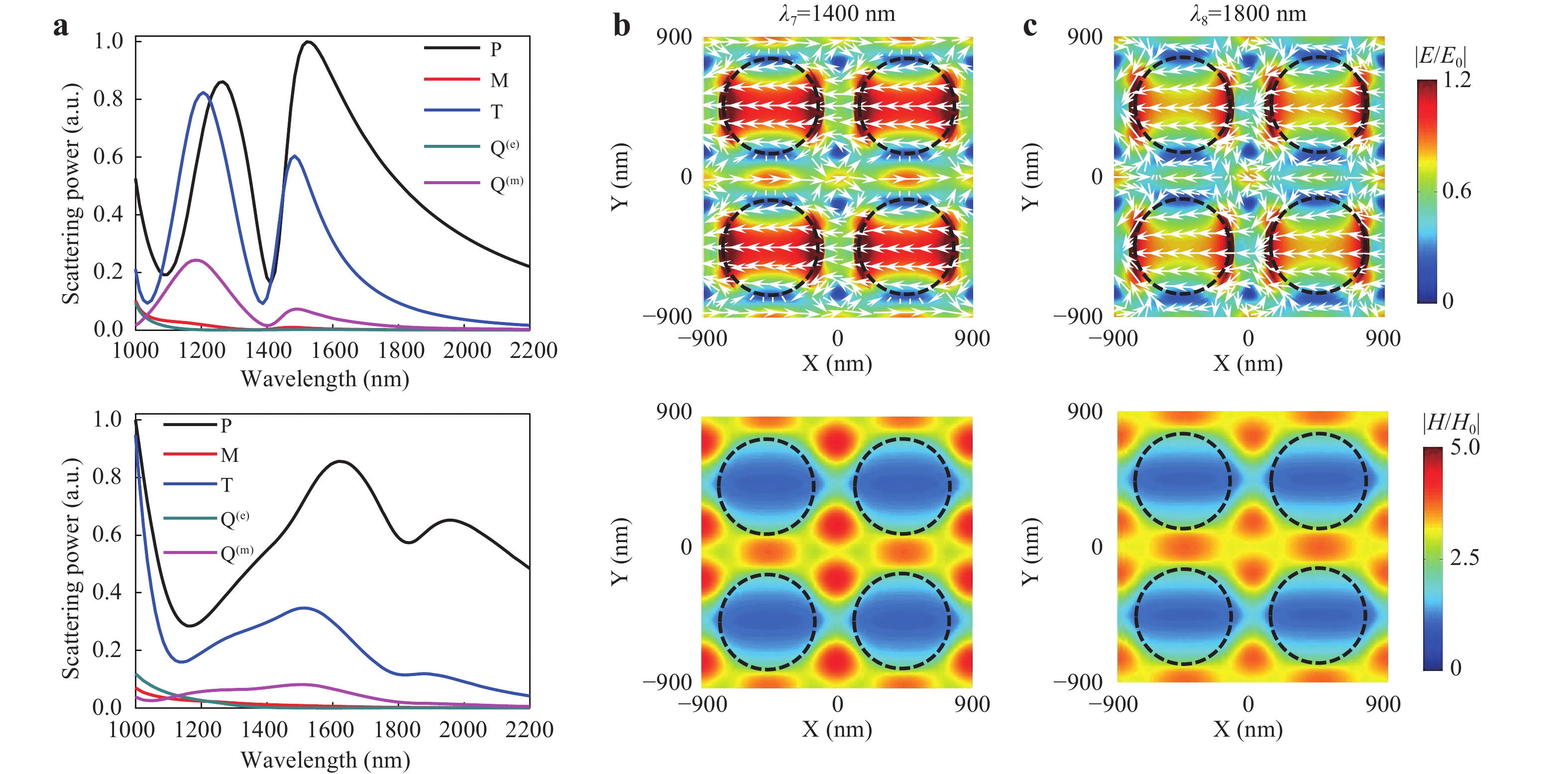
Fig. 4 Mode analysis of EIT GST225 metasurfaces with different structural states.
a Normalised scattering power of metasurface at EIT resonance modes λ7 = 1400 nm for amorphous state (top panel) and λ8 = 1800 nm for crystalline state (bottom panel). FDTD-simulated E- (top panel) and H- (bottom) field distributions at b λ7 = 1400 nm for amorphous state and c λ8 = 1800 nm for crystalline state. Arrows represent direction of surface currents, and colour scale represents corresponding intensity enhancement distribution. E0 and H0. represent electric and magnetic fields of incident light, respectively. -
The EIT response in an atomic system can yield a slow-light effect, which benefits applications in optical memory and quantum memory81. In particular, the active modulation of slow light can fulfil future controllable and densely integrated optical devices, such as slow light buffers. Herein, the slow-light feature is characterised by the group index ng of the N-IR light transmitted through the EIT metasurface, and ng can be extracted from simulations of the transmission and reflection coefficients using a well-established retrieval algorithm82, 83, as follows:
$$ {n}_{g}=\frac{c}{{\nu }_{g}}=\frac{c}{L}{\tau }_{g}=\frac{c}{L}\frac{d\varphi }{d\omega } $$ (7) where c represents the speed of light in vacuum, L the propagation distance of light in the metasurface,
$ {\tau }_{g} $ the optical delay time, ω the angular frequency, and$\varphi $ the phase shift of the transmission. Here,$ {\tau }_{g}=\dfrac{d\varphi }{d\omega } $ is defined as the ratio of the derived$\varphi $ to the angular frequency ω. Fig. 5a, b present the spectra of ng and$\varphi $ for the proposed GST225 metasurfaces at different structural states, respectively, using the Lumerical FDTD simulation. Here,$\varphi $ can be calculated using the transmission coefficient. The dispersion of the light wave becomes strong when the frequency approaches the transparent window. Subsequently, a significant shift in the phase (Fig. 5b) induced by the intense interference yields a considerable change in ng (Fig. 5a). For the amorphous GST225 metasurfaces, the maximum ng of 335 was obtained at the dip wavelength of λ9 =1500 nm, indicating that the light wave propagating through the metasurface possessed a group velocity ($ {\nu }_{g} $ ) that was 335 times slower than that in vacuum. Hence, the amorphous GST225 metasurface exhibited a slow-light effect. However, ng can be decreased significantly at λ9 = 1500 nm by changing the state of GST225 from amorphous to crystalline. Hence, we can dynamically tune ng via the phase transition of GST225. Furthermore, the reversible active tuning of ng may results in optically controllable slow-light meta-devices.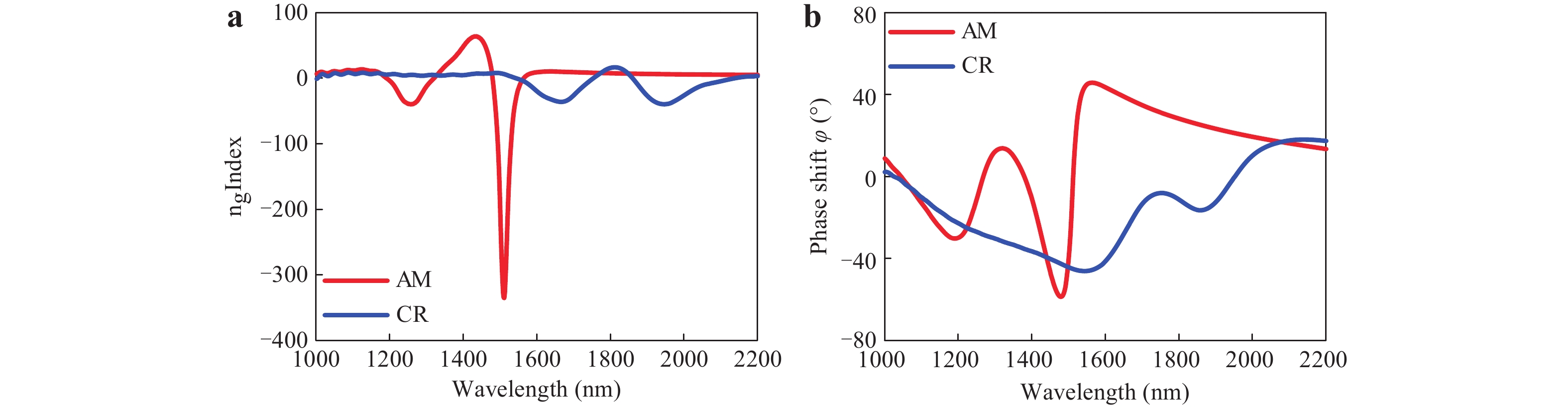
Fig. 5 Optically tunable group index ng and phase shift of transmission φ.
FDTD-simulated a ng and b$\varphi $ -
In summary, we designed and experimentally realised an all-optical and reconfigurable EIT metasurface by tuning the spectral positions of ED and TD Mie-type resonances via the phase transition of GST225, achieved via external nanosecond laser pumping. The phase change of GST225 yielded a significant contrast in the effective refractive index and enabled a resonant wavelength shift of ~360 nm in the N-IR region, where an experimental transmission relative modulation contrast of up to 80% at λ3 = 1400 nm was achieved. Although the EIT metasurface indicated strong optical modulation, our scheme involving the reversible optical switching of an all-dielectric metasurface based on GST is a general scheme that can be used in various applications. In particular, when combined with structured pumping light illumination, an appropriately designed metasurface can serve as an active metasurface for dynamic control over the wavefront of N-IR light. This can be potentially used in dynamic optical holography, active lenses, and ultrasensitive sensors.
-
Prior to deposition, a SiO2 wafer was selected as the substrate; it was ultrasonically cleaned using acetone, rinsed in isopropyl alcohol, and dried with dry nitrogen. Subsequently, a 60-nm-thick GST225 layer was sputter deposited on top of the SiO2 substrate via RF magnetron sputtering. A 99.99% pure GST sputtering target with a diameter of 50.8 mm was deposited at a rate of 0.8 Å/s via 30 W of RF power. Subsequently, a ~10-nm-thick SiO2 protection layer was deposited above the GST225 film at a deposition rate of 0.3 Å s−1. We fabricated the metasurfaces using an FEI Helios G4 UX FIB equipped with a Cobra FIB column and a five-channel gas injection system, where a Ga+ ion beam with a current of 750 pA and an acceleration voltage of 30 keV was used. The step size was set to 10 nm, which provided an excellent overlap between two consecutive spots.
-
An infrared variable angle spectroscopic ellipsometer integrated with the focusing probes was used to measure the transmittance spectra of the metasurface. The focusing probes can reduce the beam diameter on the sample from 4 mm to 200 μm to adapt to the area of the fabricated metasurface (300 μm × 300 μm). The numerical aperture of the lens of the focusing probe was ~0.01. The range of angles at which the structure was simultaneously excited was 0°–3°. The refractive indices of GST were measured via VASE. A Tauc–Lorentz model was employed to fit the VASE-measured data42, thereby minimising the mean square error (MSE) of the fitting procedure (MSE < 6)84.
-
We performed a numerical simulation of the metasurfaces using a commercially available FDTD solver (Lumerical Solutions). We adopted periodic boundary conditions in the plane (x–y plane) normal to the incident wave. Perfectly matched layer boundary conditions were applied along the vertical direction (z-axis) to terminate the simulation. We illuminated the metasurfaces vertically using a plane wave and placed a power monitor 200 nm behind the metasurface to collect the transmitted data. The structure was organised in a uniform cubic grid (2 nm × 2 nm × 2 nm), which can eliminate numerical errors. Namely, we adopted a cubic Yee cell with Δx = Δy = Δz = 2 nm, and a time step Δt = 1 × 10⁻¹⁸ s to satisfy the Courant stability85, 86. In the models, the parameters for SiO2 was based on Palik, losses were not considered in the experimental dielectric constants, and GST225 was determined based on its complex refractive index measured via VASE.
-
T.C. acknowledges support from the National Key Research and Development Program of China (2020YFA0714504,2019YFA0709100). Tun Cao and Kuan Liu contributed equally to this study.
Active tuning of electromagnetically induced transparency from chalcogenide-only metasurface
- Light: Advanced Manufacturing 2, Article number: (2021)
- Received: 15 March 2021
- Revised: 08 July 2021
- Accepted: 16 July 2021 Published online: 18 September 2021
doi: https://doi.org/10.37188/lam.2021.019
Abstract: Electromagnetically induced transparency (EIT) is a coherent optical process that provides a narrow transparent peak within a broad absorption line in an atomic medium. All-dielectric metasurface analogues of EIT have enabled new developments in the nanophotonics field for obtaining smaller, more effective slow-light devices and highly sensitive detectors without a quantum approach. However, the dynamic control of the EIT response of all-dielectric metasurfaces has been rarely reported hitherto for the near-infrared (N-IR) region, although a broader range of applications will be enabled by a reconfigurable EIT system. In this study, we realise a chalcogenide (germanium antimony telluride, GST) metasurface, which possesses a dynamically tunable EIT response by optically driving the amorphous-crystalline phase change in the GST medium. Only a few tens of nanometres thick, the nanostructured GST film exhibits Mie resonances that are spectrally modified via laser-induced phase transitions, offering a high relative modulation contrast of 80% in the N-IR region. Moreover, an extreme dispersion that results in the ‘slow light’ behaviour is observed within this transparency ‘window’. Furthermore, the group delay of the N-IR beam switches reversibly under the phase transition. The measurement is consistent with both numerical simulation results and phenomenological modelling. Our work facilitates the development of new types of compact ultrafast N-IR holograms, filtering, and ultrasensitive detectors.
Research Summary
A Tunable Chalcogenide-only Metasurface
Electromagnetically induced transparency (EIT) is a coherent optical process that provides a narrow transparent peak within a broad absorption line in an atomic medium. However, the dynamic control of the EIT response of all-dielectric metasurfaces has been rarely reported hitherto for the near-infrared (N-IR) region, although a broader range of applications will be enabled by a reconfigurable EIT system. Tun Cao from China’s Dalian University of Technology and colleagues now report a chalcogenide (germanium antimony telluride, GST) metasurface, which possesses a dynamically tunable EIT response by optically driving the amorphous-crystalline phase change in the GST medium. Only a few tens of nanometres thick, the nanostructured GST film exhibits Mie resonances that are spectrally modified via laser-induced phase transitions, offering a high relative modulation contrast of 80% in the N-IR region.


Rights and permissions
Open Access This article is licensed under a Creative Commons Attribution 4.0 International License, which permits use, sharing, adaptation, distribution and reproduction in any medium or format, as long as you give appropriate credit to the original author(s) and the source, provide a link to the Creative Commons license, and indicate if changes were made. The images or other third party material in this article are included in the article′s Creative Commons license, unless indicated otherwise in a credit line to the material. If material is not included in the article′s Creative Commons license and your intended use is not permitted by statutory regulation or exceeds the permitted use, you will need to obtain permission directly from the copyright holder. To view a copy of this license, visit http://creativecommons.org/licenses/by/4.0/.

 DownLoad: