


-
Silicon is the backbone of the microelectronics industry. Its importance in photonics requires further development owing to its indirect bandgap that precludes the efficient emission and absorption of light1. However, recent developments in nanoscience and nanotechnology in engineering have rendered silicon that approaches or even exceeds the performance of many direct bandgap materials. Therefore, nanostructured silicon offers a variety of promising applications in optical processing signals at speeds of 100 Gbit/s, detecting signals at unprecedented sensitivities for novel biosensing, trapping light for high efficiency thin-film solar cells, broadband electro-optic modulation, and perfect anti-reflection2−6. In particular, recently developed all-dielectric nano-photonics are widely based on silicon nanostructures7−10. The fabrication of subwavelength nanostructures are essential for these applications. Thus far, several nanofabrication techniques have been established11−16, including lasers interference lithography, direct laser writing and printing, self-assembly, electron beam lithography, focused ion beam milling, and plasma etching. Nevertheless, they generally require either a flat target surface, high cost, time, and complex systems, or offer limited flexibility. It is challenging to rapidly produce large-scale nanostructured surfaces using these techniques.
Alternatively, femtosecond laser-induced periodic surface structures (LIPSS) provide robust, flexible, noncontact, single-step, and potentially very low-cost methods for the fabrication of large-scale subwavelength gratings17−23. LIPSS was first observed by Birnbaum in 196524. Since the invention of femtosecond lasers, the structuring of a solid surface using femtosecond pulses has attracted growing interest from the standpoints of both fundamental and practical applications, and it is still under intensive investigation20. The femtosecond LIPSS is classified by its periodicity (Λ) with respect to the incident laser wavelength (λ)25. When Λ is slightly less than λ (0.4 < Λ/λ < 1), LIPSS are known to be low spatial frequency structures, and have been widely investigated on crystalline silicon (c-Si) wafers26−30. The orientation of femtosecond LIPSS on c-Si surfaces is prone to be perpendicular to the direction of the laser polarization. As the most accepted formation mechanism for low spatial frequency LIPSS, the initial scattering by the surface defects or existing nanostructures on the target sample leads to the generation of surface plasmon polaritons26, 31. The surface plasmons interfere with the incident laser, and thus the deposited laser energy on the material surface is periodically modulated. This spatial modulation of energy is finally imprinted in the materials and selectively ablates the parallel periodic structures31, 32.
However, in the femtosecond ablative regime, the regularity and long-range order of ripples are usually rather poor, which limits their widespread applications. This irregularity originates from the fact that, in strong optical fields, the structures are self-organized from multiple seeding points concurrently and independently. Moreover, the ablative debris and residual heat strongly influence the surface electromagnetic waves and thus reduce the quality of the LIPSS. Therefore, several ripples merge together, forming a bifurcated and disordered pattern. The usual solution to fabricating large-scale regular LIPSS is utilizing a very small laser focal spot (<10 wavelengths) to dynamically scan the surfaces and thus avoid a variation of the feature size across the spot33, 34. It remains challenging to statically process a large area with excellent long-range regularity using a large laser spot. Nevertheless, stationary irradiation is of particular interest for the generation of unconventional patterns and shapes with femtosecond structured light fields.
In this study, we solved this stubborn problem using femtosecond laser-induced low-threshold surface oxidization on amorphous silicon (a-Si) films instead of ablation. It has recently been shown experimentally that, compared to the ablative process, the oxidization on metallic thin films without material removal is capable of improving the regularity of LIPSS35−38. However, the problem of residual heat owing to the strong ohmic loss of the metals still occurs. As a much lower intrinsic absorbing material, a-Si film provides an alternative platform; however, this approach has much less explored. We found that the regular ripples on a-Si film originate from random surface oxide nanoparticles. Such particles gradually grow owing to the local field enhancement within their vicinity. Such a field enhancement is nonlinearly dependent on the particle sizes. The larger nanoparticles acquire a higher field enhancement and thus a faster growth speed, forming a positive feedback. This feedback allows the self-selection of a single seed to initiate an array of bifurcated-free one-dimensional nanograting under stationary irradiation with a large laser spot (diameter >100 wavelengths). We refer to this nonlinear feedback as an optical localization-induced nonlinear competition (O-LINC) mechanism. Furthermore, we advance the complexities and sizes of the fabricated surface structures by utilizing cylindrical vector beams, producing extremely large-scale (>500 wavelengths) radial, azimuthal, and spiral LIPSS. It should be pointed out that our non-ablative LIPSS are in a different regime from the sub-ablative ripples on Si, where the Marangoni effect plays an important role39, 40. The sub-ablative ripples originate from a phase transition process (re-solidification) rather than a chemical reaction. Unlike the ablation or re-solidification-induced grooves, the oxidization-induced LIPSS are periodic ridges, consisting of a large number of random nanoparticles. We verify that these periodic ridges can be applied in vivid structural coloring effects.
-
We illuminated a-Si film with a repetition rate of 5 kHz and pulse energy of 3.2 μJ. The laser spot diameter at the sample surface was measured to be 120 µm at an intensity of 1/e2. The average fluence was 0.028 J/cm2, which is nearly one order of magnitude lower than the typical multi-pulse ablation threshold (~ 0.2 J/cm2) of Si41, 42. After irradiating with a pulse number of Np ~ 4.5×10⁵ (90 s), we obtained a highly regular and bifurcation-free array (50 μm × 50 μm) of ripples, as shown in Fig. 1a. Their orientation was parallel to the laser polarization direction (red arrow). We found that the regular ripples can only be produced within an extremely narrow range of fluence, from 0.024 to 0.03 J/cm2. When the fluence slightly exceeds this range, the ripples become rapidly distorted and difficult to control. Fig. 1b shows the 2D fast Fourier transform (FFT) of the SEM image in Fig. 1a. A FFT analysis was conducted to obtain a more reliable value of the LIPSS periodicity. We extracted the period of the ripples from the FFT to be Λ = 952 nm, and the dispersion in the LIPSS orientation angle (DLOA) to be δθ = 6.2°. The DLOA is defined as the half-width at half-maximum value of the distribution in the FFT. A smaller dispersion angle indicates a higher regularity33, 43. It is surprising that our ripples on a-Si film produced by a large and stationary femtosecond laser beam are even more regular than almost all ripples on metals fabricated using scanning techniques with tiny laser beams33. From the high-resolution SEM image in Fig. 1c and its 2D energy dispersive X-ray spectroscopy (EDX) map in Fig. 1d, we confirmed that the laser-produced ripples arise from a periodic surface oxidization. To obtain a deeper insight, we cut them along the direction (y-axis) perpendicular to their orientation (x-axis) using a Ga+-based focused ion beam. As shown in Fig. 1e, we further verified that the ripples are accumulated by numerous micro/nanoparticles. The depth of the nanograting exceeds 100 nm.
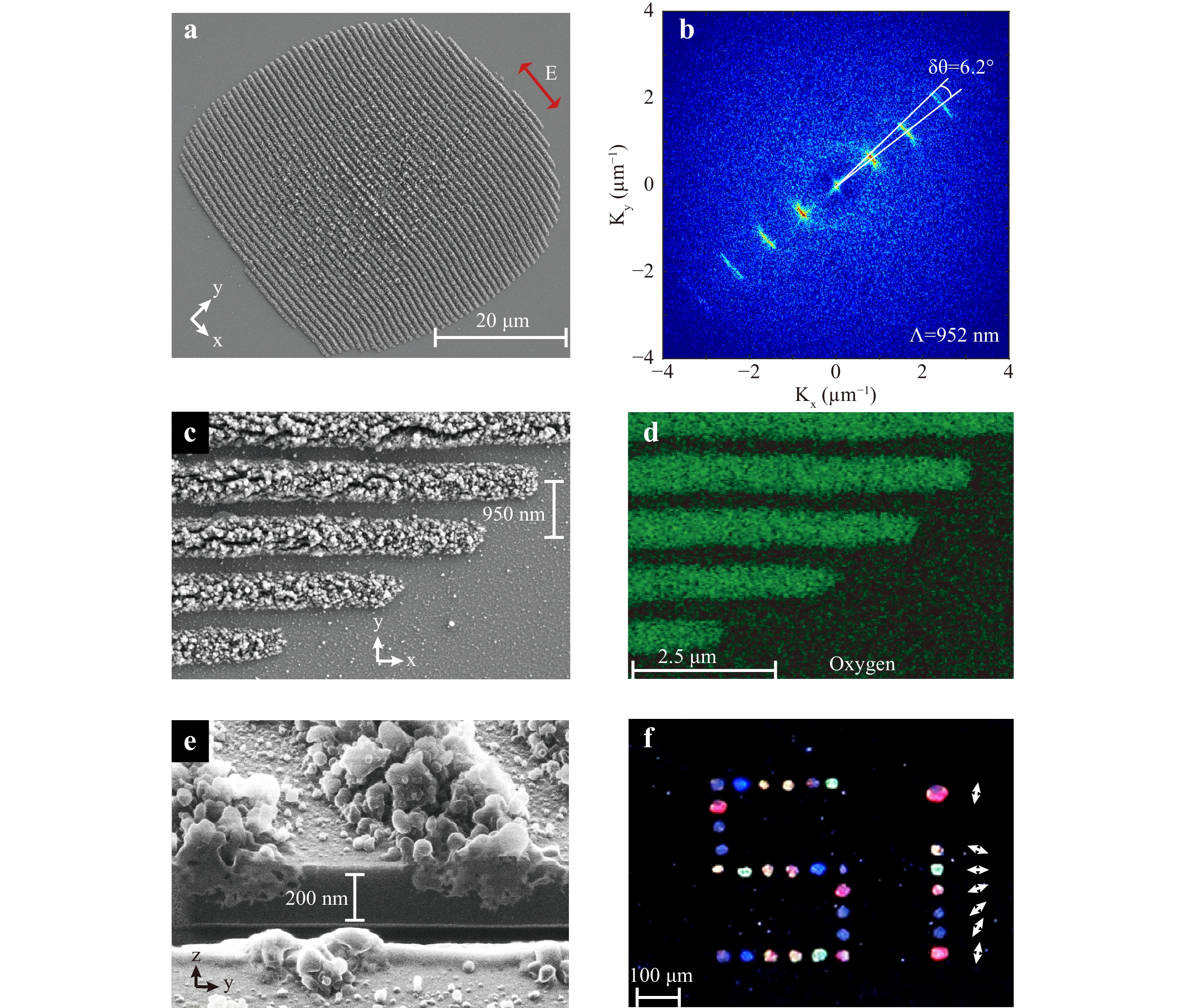
Fig. 1
a SEM image and its b 2D fast Fourier transform of femtosecond laser-inducing regular ripples on a 200-nm thick a-Si thin film. The red arrows denote the laser polarization direction. c High-resolution SEM image and corresponding d EDX map of a representative LIPSS, which illustrate that the ripples arise from periodic surface oxidization. The periodicity of the ripples is measured to be 950 nm. e In situ cross-sectional imaging of the ripples milled by a Ga+-based focused ion beam. f Optical microscopy image of a set of LIPSS produced through various laser polarization directions (arrows), forming a colorful element symbol "Si".Such a highly regular 1D grating-like LIPSS can be applied under the structural coloring effects. A more regular LIPSS pattern will tend to display a better coloring effect because the colors arise from the grating-induced light diffraction. For instance, by controlling the laser polarization, we produce a set of LIPSS with various orientations, forming a colorful element symbol “Si”, as shown in Fig. 1f. Each color produced by a stationary laser beam can potentially behave as a pixel to compose more complex surface patterns. In Fig. 1f, the red, yellow, green, and blue structural colors are all extremely homogeneous and bright. Usually, the structural color of blue on the Si looks dark and blue-green owing to its strong absorption and the scattering of blue light22. However, the bright blue in our case confirms that the highly regular oxidation-based LIPSS is capable of improving the structural coloring effects. The durability and stability of the oxidized ripples are of concern. We confirmed that they can withstand exposure in an ultrasound machine with solvents such as methanol and acetone without any noticeable loss in performance.
Surface plasmon-assisted LIPSS require their orientation to be perpendicular to the laser polarization43−45. However, the orientation of our nanograting was along the laser polarization. Therefore, the role of surface plasmons was excluded in our experiments. To better understand the mechanism of this long-range regularity, we investigated the surface structuring before the formation of the LIPSS. As shown in the SEM images in Fig. 2a, we observed several random laser-produced nanoparticles and a periodic distribution of the surface patterns. The latter originates from the interference of the incident/reflected fields with waves scattered by the nanoparticles. These were confirmed through the FDTD-based numerical simulation shown in Fig. 2b. If newly oxidized nanoparticles are created in the constructive interference areas, their nonlocal feedback disturbs the interfering patterns, as shown in Fig. 2d. Fortunately, owing to the ultralow laser fluence, we found that the periodic interfering patterns shown in Fig. 2a may be imprinted only by laser-induced surface crystallization, rather than by oxidization, as verified by the EDX map in Fig. 2c. Therefore, unlike their metallic counterparts35 nonlocal feedback from the scattering fields is insignificant on the Si films.
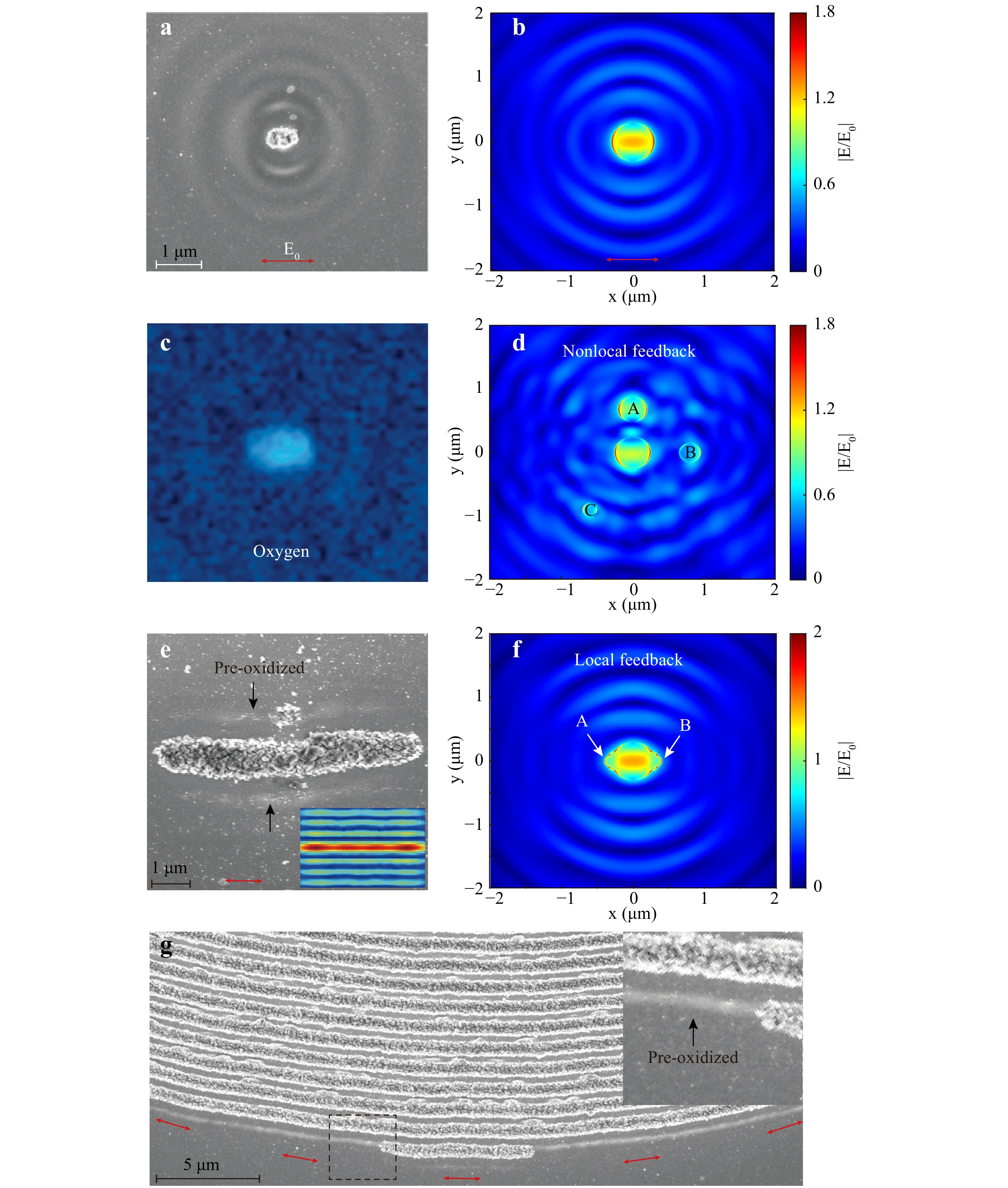
Fig. 2
a SEM image of laser-produced nanoparticle and interfering patterns on a 200-nm thick a-Si film. Red arrows indicate the laser polarization direction. b Numerical simulation of interfacial electric field distribution on 200-nm thick a-Si film with an embedded SiO2 nanoparticle. The diameter of this particle in the x–y-plane is set to 500 nm. c 2D-EDX map of oxygen demonstrates that the oxidization process only occurs within the large nanoparticles but not in the constructive interfering regions. d When a large particle is surrounded by several smaller ones, the nonlocal feedback leads to a distorted interfering pattern. The diameters of these smaller particles in the x–y-plane are A = 400, B = 300, and C = 200 nm, respectively. e SEM image of a laser-produced oxidized stripe. Two weakly presented nano-lines that are parallel to this stripe are observed, as indicated by the black arrow, which originate from the interference between the incident and the scattering waves by the stripe. They are labeled a pre-oxidized structure. Inset: Simulation of interfacial electric field distribution with an embedded SiO2 stripe. f Simulated electric field distribution with an enlarged elliptical SiO2 nanoparticle. Two nanoparticles (indicated by A, B) with a diameter of 100 nm are placed at the poles of the particle in b, representing the growth of oxide owing to field localization. The light source in all simulations is a plane wave at 1030 nm, and polarizes along the x-axis. g SEM image of curved stripes that are produced by structured optical fields. The red arrows indicate the local electric field directions. The dashed area is enlarged in the inset.Alternatively, we believe that the large-scale regularity arises from the O-LINC mechanism. An interfacial electric field enhancement is highly localized at the two poles of a nanoparticle along the laser polarization direction, as shown in Fig. 2b. The numerical simulation is shown in Supplementary Fig. S1. Therefore, oxidization will preferentially extend to along the polarization direction, as the first step. When irradiating with circular polarization, we cannot obtain the periodic ripples because the oxidized nanoparticles grow in every direction (Supplementary, Fig. S2). The scattering intensity Is when using a Rayleigh scatter is proportional to the local laser intensity I(x, y) and the square of the particle volume V, that is, Is ~ V2 × I(x, y). Owing to the Gaussian distribution of the laser intensity, the larger nanoparticles closer to the beam center will always acquire a higher scattering power, and thus a higher initial growth rate. As the nanoparticles grow, so do their scattering intensity at the poles, resulting in local feedback (Fig. 2f). Consequently, the ratio of the volume of the biggest nanoparticle to that of the surrounding smaller ones will increase nonlinearly over the irradiation time, featuring a nonlinear competition process. This O-LINC mechanism, schematically illustrated in Supplementary Fig. S3, ensures the selection of a single seed within a large area.
Once a nanoparticle has grown into a stripe, it acts as a collimator to regulate the spaced nano-lines that are parallel to the laser polarization (see the SEM image and inset in Fig. 2e). An in situ optical microscopic observation of the LIPSS evolution process is shown in Supplementary Movie S1. This directly confirms that a large-area nanograting is grown from a single seed. This optical localization-induced polarization-sensitive growth of oxide was further confirmed using a laser with spatially varying polarization. As shown in Fig. 2g, the orientations of the stripes always follow the electric field directions (red arrows). More importantly, the bottom pre-oxidized nano-line in the SEM image in Fig. 2g and the enlarged area in the inset illustrate that the existing stripes have a highly localized influence on the neighboring electric field. The high localization of the electric field among both the nanoparticles and within the vicinity of the nano-stripes ensures a highly uniform LIPSS generation within a large area.
The regularity of the LIPSS can be further improved using an artificial seed. We employed a commercially available micro-Raman spectroscopic system to etch a nanogroove on an a-Si film, as indicated by the blue arrow in Fig. 3a. The depth of this groove was measured to be 5 nm using an atomic force microscope (Fig. 3b). When subsequently illuminated using a femtosecond laser with a polarization along the nanogroove, the oxidization process is confined inside the pre-structured nanogroove, where the optical field is localized, as indicated by the black arrow in Fig. 3a. The oxidized stripe has a height of 180 nm (Fig. 3d). We found that the artificial seed will efficiently lower the threshold for oxidization, resulting in a much cleaner surface than that without artificial seeds, as confirmed by the dark-field optical microscopy image in Fig. 3c. This highly collimated seeding structure regulates the growth process of the LIPSS and can thus significantly further improve their regularity.
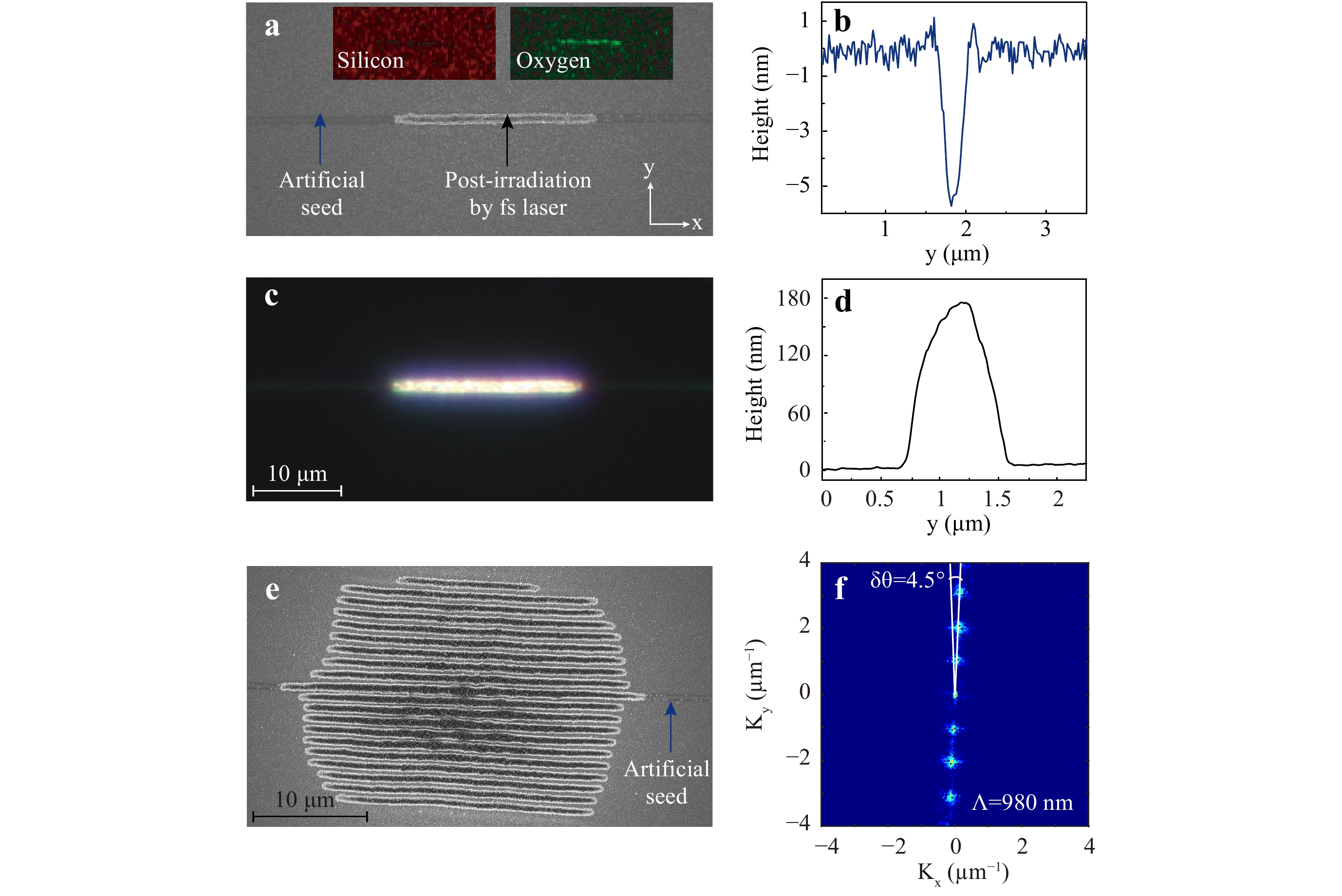
Fig. 3
a SEM image and c dark-field optical microscopy image of a nanogroove etched using a 532-nm CW laser as an artificial seed, and subsequently irradiated by a femtosecond laser. Owing to the nanogroove-induced optical localization, the initial oxidization process is confined within the nanogroove. The heights of the artificial seed b before and d after femtosecond laser irradiation, as measured using an atomic force microscope. e SEM image and its f 2D Fourier transform of a highly regular periodic ripples that are regulated using an artificial seed. Please note that the orientation of the seed is not strictly parallel to the laser polarization direction. The produced periodic ripples are along the orientation of the seed.As a next step, we demonstrated that this O-LINC mechanism allows us to obtain more complicated large-area LIPSS patterns using cylindrical vector beams produced by a vortex waveplate. Fig. 4a−c show overview of SEM images of LIPSS produced through azimuthal, spiral, and radial polarizations. Their 2D-FFT is given in the insets, which indicate a high regularity along each orientation direction. The structures inside the white boxes in Fig. 4a−c are enlarged in Fig. 4d−f, respectively. We confirm that in all cases, the oxidized ripples show excellent growth along the laser polarization direction. Compared to the structured light-field-induced ablative ripples28, 46, the oxidized ripples exhibit significantly higher regularity in much larger areas. Fig. 4g−i show optical microscopy images of even larger structures that are also produced by vector beams. A set of white light sources shining from different angles was employed to obtain the colorful images. This angle-dependent vision confirms that the structural colors arise from the long-range periodic ripples rather than the local micro/particles, because the latter are independent of the angle of incident light22. Please note that the outer diameters and areas of the surface patterns shown in Fig. 4g−i reach up to d = 500 µm and 0.2 mm2, which are only produced by ~1.5 × 10⁶ pulses. Owing to the direct utilization of a large beam spot in our case, the fabrication speed was nearly four orders of magnitude higher than those reported elsewhere35. Moreover, it is challenging to fabricate a large-scale sophisticated pattern such as the anticlockwise structure shown in Fig. 4i using a typical scanning technique because each ridge has a different radius of curvature and orientation. The anticlockwise surface pattern may be of interest owing to the optical chirality47, 48. An analysis of the surface structures can also offer a useful approach to the characterization of an intense and complex light field.
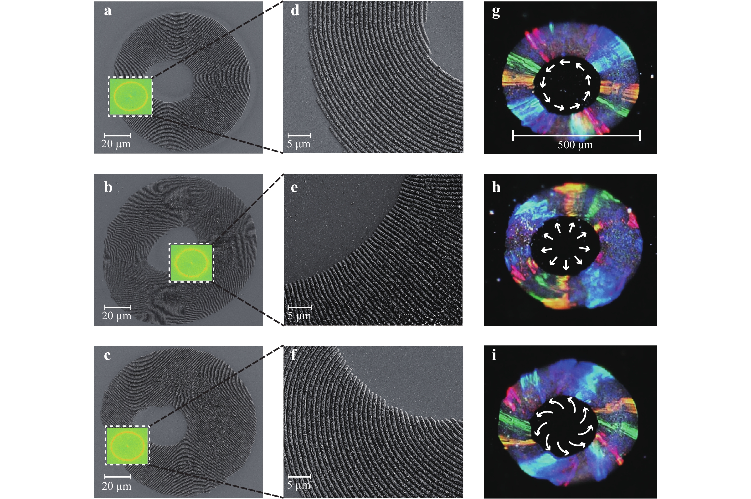
Fig. 4
Overview SEM images of LIPSS patterns produced by a stationary laser beam focused by a focal length of 20 cm with a azimuthal, b radial, and c spiral polarizations, respectively. The insets display their 2D Fourier transforms. d–f Zoomed-in structures inside the dashed boxes in a–c, respectively. g–i Optical microscopy images of LIPSS patterns produced by a stationary laser beam focused by a focal length of 20 cm while not at the focal spot with azimuthal, radial, and spiral polarizations, respectively. The vivid colors of the large-scale patterns indicate the highly regular subwavelength periodic structures inside LIPSS.To summarize, we demonstrated experimentally that by carefully adjusting the incident power to a critical fluence, it tends to form a single effective seed location on 200-nm thick a-Si films, initiating a large-scale but extremely regular, bifurcation-free, oxidized LIPSS through an O-LINC mechanism. This mechanism is induced by the oxidized nanoparticle-induced optical localization, promoting the gentle growth of oxidized stripes preferentially along the laser polarization direction. More interestingly, we confirmed that the ripples can be further regulated by an artificial seeding groove. Using a large sized stationary laser beam, we successfully produced fantastic ripples with linear, radial, and azimuthal polarizations, respectively. We showed that these oxidized ripples are durable and stable, which render them appealing in the applications of non-plasmonic structural coloring, antireflective effects, and multi-dimensional metasurfaces for use in holographic technologies49.
-
We carried out the experiments using a diode-pumped ultrafast fiber amplifier system (Amplitude) delivering a central wavelength of 1030 nm and a pulse duration of 130 fs. The laser repetition rate was set to 5 kHz. The laser beam is focused onto the target sample through a convex lens with f = 20 cm. The diameter at the laser focal spot is measured to be 120 µm using a CCD camera beam profiler. An industrial camera is utilized for real-time monitoring of the surface structuring process. When the surface structures appear, it will strongly scatter the light. An optical microscope is employed in situ to observe the growth process of the nanograting. A half-wave plate combined with a linear polarizer is employed to control the pulse energies. A vortex waveplate is used to obtain the vector beams.
-
The a-Si films are evaporated with a magnetron sputtering system (ULVAC CS200Z) at a power of 300 W, temperature of 300 °C, pressure of 0.3 Pa, Ar flow rate of 70 sccm from the silicon target with a diameter of 100 mm located at a distance of 90 mm with a deposition rate of 5.66 nm/min.
-
The colorful optical microscopy images were recorded using a super-resolution digital microscope (Keyence, VHX-6000). Several white light sources irradiated from different angles were utilized to obtain the structural colors of the LIPSS.
-
SEM images and two-dimensional EDX were captured using a field-emission scanning electron microscope (Carl Zeiss, Gemini450). The milling and in situ imaging of the cross-sectional view of the silicon ripples were carried out using a focused ion beam (Carl Zeiss, Orion Nano Fab).
-
The artificial seeding nanogroove was etched using a commercially available micro-Raman spectroscopy system. The wavelength of the laser is 532 nm, and the laser achieves a spatial etching resolution of 350 nm.
-
This research was supported by the National Key Research and Development Program of China (2017YFA0205700), and the National Natural Science Foundation of China (No. 61927820, No. 12004313, No.12004314). Liping Shi is supported by the open project program of Wuhan National Laboratory for optoelectronics No. 2020WNLOKF004 and Zhejiang Provincial Natural Science Foundation of China under Grant No. Q21A040010. The authors are grateful for the technical support from the Center for Micro/Nano Fabrication, as well as from the Instrumentation and Service Center for Physical Sciences at Westlake University. We also appreciate Dr. Wei Yan and Dr. Jiuan Lv from Westlake University, Prof. Tianqing Jia from East China Normal University, and Prof. Yi Liu from the University of Shanghai for Science and Technology for the fruitful discussions, and Yingchun Wu for technical support in a focused ion beam.
Controllable generation of large-scale highly regular gratings on Si films
-
Jiao Geng1, 2,
 ,
, - Xiaoguo Fang1, 2,
- Lei Zhang1, 2,
- Guangnan Yao1, 2,
- Liye Xu1, 2,
- Fengjiang Liu1, 2,
- Weiwei Tang1, 2,
-
Liping Shi1, 2, ,
,
-
Min Qiu1, 2, *, ,
- Light: Advanced Manufacturing 2, Article number: (2021)
- Received: 01 April 2021
- Revised: 27 July 2021
- Accepted: 06 August 2021 Published online: 22 September 2021
doi: https://doi.org/10.37188/lam.2021.022
Abstract: The application of femtosecond laser-induced periodic surface texturing has significant potential in medicine, optics, tribology, and biology, among other areas. However, when irradiated by a large intense laser spot, the periodic structures usually exhibit an uncontrollable regularity, forming bifurcated patterns, thus limiting their widespread application. Irregularity originates from numerous independent branching seeds. The usual solution to this problem is to utilize the quasi-direct laser writing technique, that is, by limiting the laser beam size (diameter of <10 wavelengths) and scanning the beam or samples using 2D translation stages. Herein, we demonstrate an optical localization-induced nonlinear competition mechanism to solve this problem, which occurs at a fluence nearly one order of magnitude below the ablation threshold. Owing to the low intrinsic absorption of silicon and ultralow applied fluence, this mechanism ensures the self-selection of a single seed to initiate an array of bifurcated-free gratings under stationary irradiation with a large laser spot (diameter >100 wavelengths). Surprisingly, some unconventional complex patterns, such as radial, annular, and spiral gratings, can also be easily produced by structured light fields with unprecedented regularity. Their diameters reach up to >500 μm. Moreover, we can artificially control the initial seeding structure to further improve the regularity of the gratings, defined by dispersion in the ripple orientation angle in their 2D Fourier transform. As a result, the regularity in our experiments produced by a large laser spot is even higher than that scanned by a tiny beam. Controllable and highly regular ripples are beneficial to the structural coloring effects because they arise from the light diffraction by subwavelength gratings.
Research Summary
Laser-induced Oxidation: thermochemical process for controllable nanofabrication
Femtosecond laser-induced periodic surface micro/nano texturing shows promise for many areas. However, its quality control is a stubborn problem, which arises from residual heat and numerous ablative debris as random seeds. Min Qiu from China’s Westlake University and colleagues now report an optical localization-induced nonlinear competition mechanism to solve this long-standing problem. This mechanism is upon laser-induced oxidation instead of ablation. The oxidation, a non-ablative thermochemical process, has much lower threshold, avoiding the ablative debris as well as residual heat. It ensures self-selection of a single seed to initiate a large array of bifurcated-free periodic nanostructures. Moreover, the team demonstrated the use of artificial seed to control the growth of the periodic surface oxidation process, further improving the quality of the periodic surface nanostructures. The authors illustrate their applications in structural coloring effects.
Rights and permissions
Open Access This article is licensed under a Creative Commons Attribution 4.0 International License, which permits use, sharing, adaptation, distribution and reproduction in any medium or format, as long as you give appropriate credit to the original author(s) and the source, provide a link to the Creative Commons license, and indicate if changes were made. The images or other third party material in this article are included in the article′s Creative Commons license, unless indicated otherwise in a credit line to the material. If material is not included in the article′s Creative Commons license and your intended use is not permitted by statutory regulation or exceeds the permitted use, you will need to obtain permission directly from the copyright holder. To view a copy of this license, visit http://creativecommons.org/licenses/by/4.0/.

 DownLoad: