


-
In recent years, augmented reality head-mounted displays (AR-HMDs) have been widely considered as the “black technology of the future.” However, they are not a new concept1−7. While virtual reality (VR) and augmented reality (AR) are frequently used interchangeably, they are distinct concepts. VR-HMD technology places users in a completely virtual world generated by computers, such as in games, movies, and live broadcasts. However, AR-HMD technology enables users to simultaneously see real-world scenes in front of them and virtual objects generated by computers1,4. AR-HMDs use optical combiners and display devices to project virtual objects onto real-world ones. The most common method employed for this is the use of transparent optical elements, which ensure that both virtual and real images can reach the human eyes simultaneously. The emergence of smartphones has accelerated the miniaturization of integrated circuits and the advancement of high-performance display devices. The emergence of high-resolution and high-brightness microdisplays has resulted in the popularity of AR-HMDs increasing8,9. Because they have subversively upgraded user experience, AR-HMDs are considered to be the “next generation platform” after the widespread use of intelligent communications and computing terminal devices, such as PCs and smartphones. AR-HMDs augment the physical world by superimposing sound, video, graphics, and navigation data over it in real time, providing information that assists people in their work and life. AR-HMDs are currently widely employed in the fields of medicine10,11, aviation6,12, manufacturing13, information acquisition, and entertainment1,2,14. Most of the research in this field is now focused on the development of optical see-through AR-HMDs. This article reviews the current methods for developing optical see-through AR-HMDs.
AR-HMD manufacturers today still encounter significant challenges. An AR-HMD is a head-mounted device, and a large-volume and large-weight system is not suitable for people to wear for long periods. Thus, an AR-HMD that is ergonomic and offers optical system solutions is required. Owing to the limitations of processing technology, early optical systems were required to correct large aberrations using many spherical lenses, which increased the weight of the system. In addition, because an AR-HMD is a visual display, its related parameters are based on the human eye. The size of the eyebox restricts the human eye to the virtual images within a certain spatial range. Furthermore, industries such as aviation, manufacturing, and entertainment urgently require AR-HMDs with large fields of view (FOVs) and high resolutions1−4. However, simultaneously achieving a large FOV and high resolution is difficult, and the development of methods to achieve this constitutes a major technical challenge. The spectral bandwidth of microdisplays must also match the sensitive spectral region of the human eye, and commercial applications generally require AR-HMDs to have full-color display capabilities. This results in the problem of having to eliminate or correct chromatic aberrations, by means such as using the diffraction waveguide mentioned later in this review15. In addition, the microdisplay is required to have a larger brightness adjustment range within the comfort range of the human eye to form sufficient brightness contrast between the external environment and virtual information when the human eyes receive virtual information. Moreover, the optical see-through must be such that the AR-HMD has sufficient optical transmittance. Although the advancements in liquid crystal on silicon (LCOS), organic light-emitting diodes (OLEDs), and other such microdisplays have overcome the limitations of display brightness to a certain extent, high light efficiency and optical transmittance are still important. In other words, AR-HMDs must have full color, large FOVs, high resolutions, and undistorted perspectives projected over real scenes for a high-presence virtual and real fusion display to be achieved. Furthermore, for AR-HMDs to be worn comfortably, the optical system thereof must involve a large eyebox. Owing to these optical requirements, developing an AR-HMD optical system with a large FOV and large numerical aperture (NA) is difficult.
-
Classifying AR-HMDs using the concept of optical design is difficult. In optical design, the performance evaluation indicators of AR-HMD primarily include the FOV, eyebox, light efficiency, transmittance, modulation transfer function (MTF), distortion, volume, and weight1−8,16. In the early years, optical designs based on reflective and refractive lens elements were used for mainstream AR-HMDs to deliver high-brightness display images to the eyes. Limited by the processing technology and design methods, these early solutions adopted simple rotationally symmetric coaxial optical-imaging systems. However, these techniques cannot satisfy increasing demands, such as a large FOV, high resolution, and thin structures4,5.
With the development of processing technology, design methods, and surface-description methods for freeform surfaces (FFS)17−22, off-axis refractive and reflective structures based on aspheric surfaces (AS) and FFS have been developed. This has also prompted the development of several catadioptric AR-HMD solutions4. AS and FFS can correct most aberrations in optical-imaging systems. While expanding the FOV and achieving high resolution, they can also render the structure lighter and compact18−23. The development of high-precision optical-injection processing technology guarantees mass production of aspheric and freeform optical lenses. Therefore, AR-HMDs based on AS and FFS systems have been the first to meet commercial production specifications in recent years24−29. The use of AR-HMDs that are based on geometric optical waveguides can result in thinner and lighter systems, and their characteristics are closer to those of prescription glasses. However, significant challenges and difficulties arise in terms of illumination uniformity, stray-light suppression, and expansion of the FOV. In addition, achieving mass production is difficult because of their complicated processing technology30,31. Owing to the limitations of optical invariants, it is difficult for optical catadioptric types of AR-HMDs to simultaneously satisfy the design requirements of large FOVs, large exit pupil diameters (EPDs), and compact systems3,4.
The introduction of diffractive optical elements into AR-HMD systems have attracted significant interest. When a light beam is incident at a certain angle, the diffractive optical element can provide a larger beam deflection angle when compared with that in the case of geometric refraction and reflection32. In 1996, diffractive optical elements were used in AR-HMDs to reduce system weight and optical aberrations. A diffraction waveguide AR-HMD was developed for surface relief grating (SRG) waveguides and volume hologram grating (VHG) waveguides after more than ten years of development. The developed AR-HMD, which has a thin and light waveguide shape, depicts the ideal shape of future AR-HMDs. Planar diffractive waveguide technology has become a popular focus of research because of its advantages with respect to its form factor and large EPD. AR-HMDs of consumer electronics products are also becoming popular research targets. However, the current diffraction-waveguide AR-HMD still has many drawbacks, such as low efficiency, chromatic aberration in full-color displays, illuminance non-uniformity, and lack of mass production processing technology, which hinder its commercial application33. Furthermore, liquid crystal (LC)-based grating and polarization volume grating (PVG) structures have been studied and developed34,35. The PVG is constructed using an LC film, and it can achieve a light-diffraction efficiency close to 100%. The application of metalenses in AR-HMDs has also attracted research interest owing to their strong capabilities in wavefront phase control and the geometric characteristics of planar elements36,37.
As shown in Fig. 1, this review introduces the current solutions involving AR-HMD optical combiners, mainly in three broad categories: macro-, micro-, and nanooptical solutions, introduced in Sections 3.1, 3.2, and 3.3, respectively. Macro optical solutions include traditional optical, freeform prism, and geometric optical waveguide solutions, which are based on Snell’s law of refraction and reflection. Microoptical solutions include SRG, VHG, and PVG diffraction grating optical solutions, which concern the light deflection effects of grating diffraction. Finally, nanooptical solutions include metalens and metasurface reflector solutions, which are based on phase modulation effects on nanoscale microstructures.
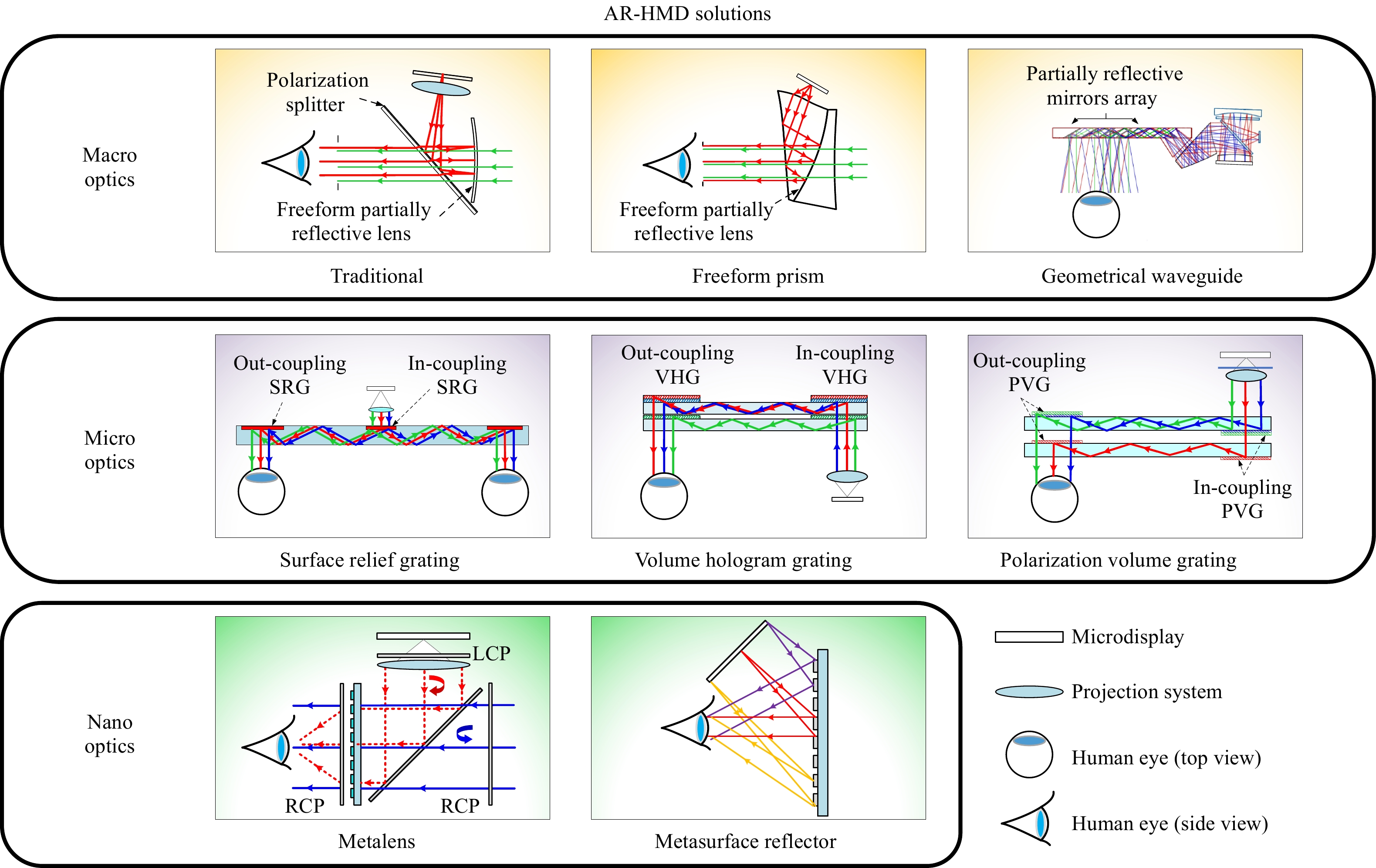
Fig. 1 Basic classification of AR-HMD optical solutions.
-
Traditional AR-HMD optical systems are frequently designed using spherical, aspheric, and FFS optical elements in consideration of Snell's refraction law. Representative traditional AR-HMD optical solutions are shown in Fig. 2. Fig. 2a shows an optical transmission AR-HMD based on the traditional eyepiece structure. Early augmented display optical systems simply included a plane split-coupling element based on the traditional eyepiece. Through this coupling element, virtual information and the real environment were merged to achieve a functioning AR display. Fig. 2b shows another form of this structure. After the light source brightens the LCOS, the light irradiates the prism, passes through the partially reflective plane twice, and enters the human eye. Because of its simple and lightweight structure and high processing feasibility, it can be rapidly mass-produced in commercial quantities and has been successfully applied in fields such as interaction and navigation14. Google Glass23 AR-HMD is based on the half-mirror solution with a horizontal FOV of 13° and resolution of 640 × 360. However, the FOV is significantly affected by the thickness and length of the prism, and the maximum FOV achieved is approximately 20°. Furthermore, the EPD is relatively small, which means that the human eye should be positioned close to that of the optical system. A larger FOV can however be achieved by adopting several AR-HMD optical solutions12,19,22 (Fig. 2(c)). The relay projection lens group primarily provides the focal power, which can increase the imaging FOV. Furthermore, this AR-HMD optical solution has a high optical transmittance, larger eyebox, and larger EPD. However, the off-axis layout introduces asymmetric aberrations, which are not easily corrected using traditional axisymmetric systems or AS. Although FFS are used to optimize the design to further correct aberrations and improve the image quality, the system structure is still bulky, and the large asymmetry distortion is an inherent defect of the optical solution. L-3 AR-HMD system12 based on this optical solution achieves an optical transmittance of over 60%, an FOV of 100° × 50°, and an EPD of more than 50 mm, but the system weight is approximately 2700 g. As shown in Fig. 2d, the off-axis AR-HMD realized using the freeform partially reflective lens is characterized by a light weight, and the FOV of the system can reach 90°. As the imaging optical element in the system is only a piece of the FFS, it can significantly decrease the weight of the system and relieve users from heaviness. However, it is difficult to correct many off-axis aberrations in the system using only one FFS, and it is even more difficult to correct the aberrations at the edge FOV, which also introduces a large distortion4. Meta 2 is an AR-HMD product obtained using this optical solution, and it achieves a 90° FOV with a resolution of 2.5 K24; however, its system structure is bulky.
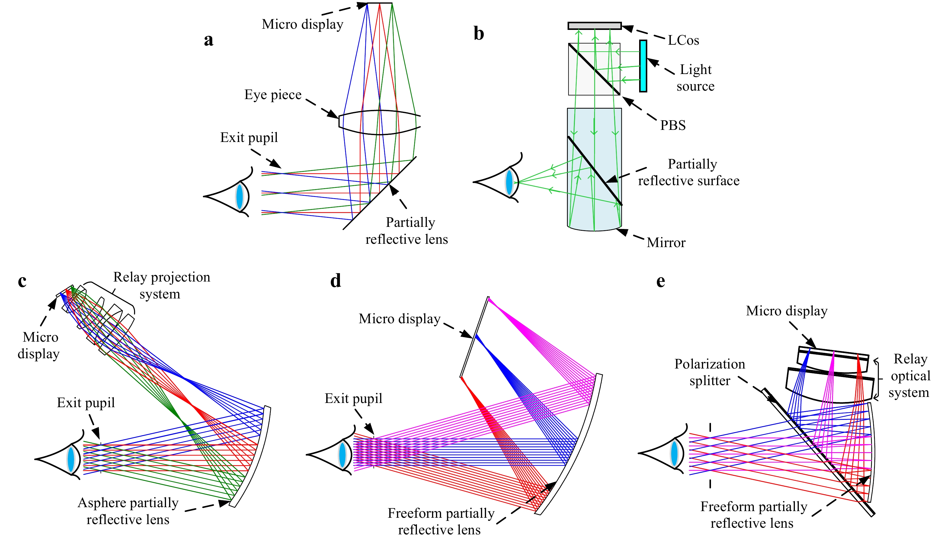
Fig. 2 Several common AR-HMD solutions.
a Schematic of the optical path of traditional eyepieces; b schematic of simple half-mirror solution; c schematic of a relay projection optical solution; d schematic of first-order an off-axis aspheric reflective optical solution; e schematic of the BirdBath optical solution.The BirdBath optical solution uses two coupling elements to realize the function of the augmented display, which achieves high image quality and large FOV, and it is a compact structure. The name “birdbath” is derived from the spherical mirror/combiner being similar to a typical birdbath. As shown in Fig. 2e, this AR-HMD system includes a planar split-coupled element and a curved split-coupled element. Through the two coupling elements, the image from the microdisplay is projected over the real-world view. The maximum theoretical optical efficiency of this system is only 12.5%. Theoretically, the optical efficiency of the system can be increased to 25% using a polarization splitter (PS) film, quarter-wave plate, and polarizer. A PS is bonded to the plate glass, the quarter-wave plate is then bonded to the PS, and the polarizer is bonded to a microdisplay/relay lens. In the BirdBath solution, although the optical axis direction is turned several times, coaxiality of the lens still features in the optical system, thus significantly decreasing the aberration owing to the introduction of an off-axis structure. To improve the display effect of the system as much as possible, curved surface split-coupling elements and lens groups are frequently used with an aspheric surface to increase the optimization variables in the system. Daystar G2 AR-HMD25 of Lenovo company is based on the BirdBath solution38, which uses two aspheric lenses. It achieves a monocular FOV of more than 50° and an image distortion of less than 1%. In addition, the total weight of the lens is less than 20 g, and the overall structure is compact.
-
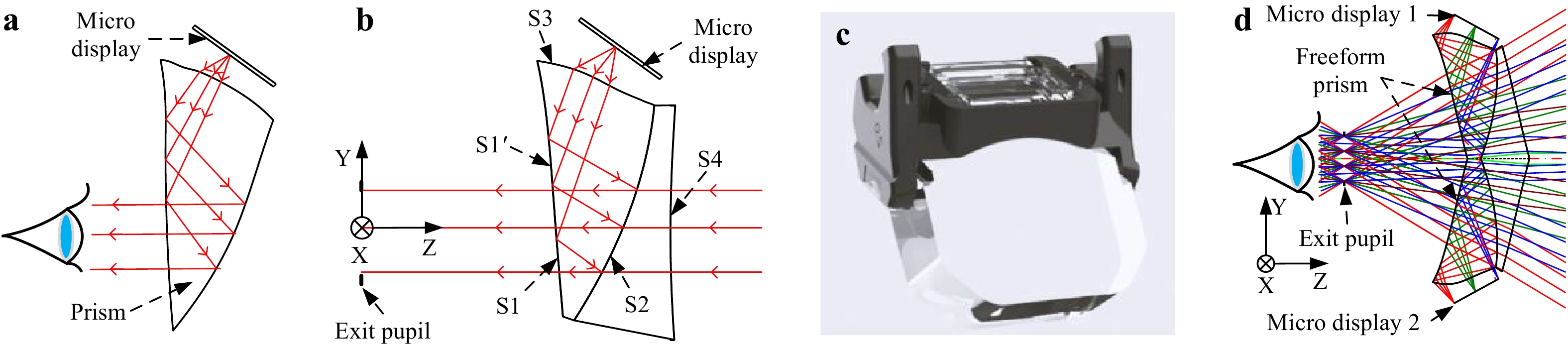
The development of FFS design methods has prompted the development of various optical designs17−22. Owing to its small size and light weight, the freeform prism can achieve a large FOV, high resolution, large EPD, and see-through display25−29. The Japanese companies Olympus25 and Canon26 applied for patents of the freeform wedge prism optical systems in 1995 and 1996, respectively. Its structure is shown in Fig. 3a. However, the system is large, the FOV is small, and the resolution of the microdisplay is low. Cheng et al.27 proposed a specific design method for an AR-HMD based on a freeform prism and introduced a new structure composed of a freeform wedge prism and a freeform see-through compensation lens. As shown in Fig. 3b, the light from the microdisplay passes through surface 3 of the freeform prism and projects into the prism interior. Subsequently, because of the total internal reflection (TIR) condition on surface 1', the light reaches surface 2 and is again reflected. It then passes through surface 1 again, and finally leaves the prism and enters the human eye. The light from the real scene is transmitted into the human eye through a freeform see-through compensation prism (between S2 and S4) and a freeform prism (between S1 and S2). Fig. 3c shows the optical module of the freeform prism. Later, Cheng et al.28 proposed a splicing freeform prism that further increased the monocular display FOV of AR-HMDs, and reaching 82° ×32° (Fig. 3d). In addition, NED Ltd. developed a binocular-integrated AR-HMD optical module with a diagonal FOV of 120° and an EPD of 8 mm29.
Freeform optical prisms have complicated polyhedral properties. Thus, the peak-valley (PV) precision, roughness, eccentricity, and tilt precision of all optical surfaces should be simultaneously considered during the optimization and production processes. Fig. 4 shows a flow chart of the design, optimization, and manufacturing of the FFS optical system. The complete process can be divided into nine steps:
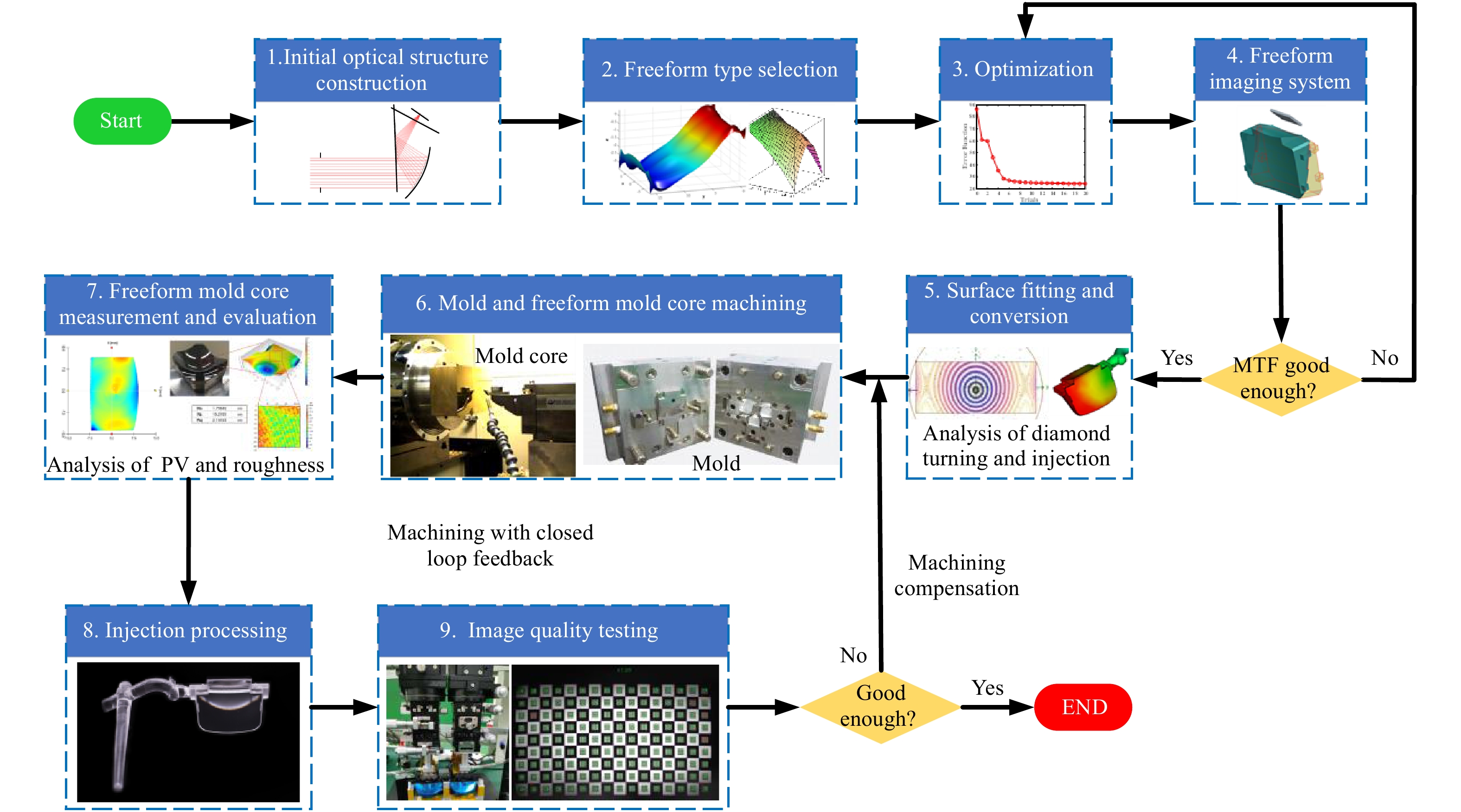
Fig. 4 Schematic diagram of design, optimization, and machining process of FFS element.
(1) Initial optical structure construction: The initial optical structure should be constructed first.
(2) Freeform type selection: The surface expression of FFS should be determined.
(3) Optimization: The image quality and structure of the optical system should be optimized to satisfy the requirements by controlling the boundary conditions and surface parameters.
(4) Optimized freeform prism optical imaging system: The optimized optical structure is generated, and the rationality of the optical structure is analyzed.
(5) Surface fitting and conversion: Surface fitting and conversion are required for feasibility analysis before machining. Moldflow software has been used to conduct a simulation analysis of the product's process conditions and to confirm the suitability of the mold design39.
(6) Mold and freeform mold core machining: Currently, FFS machining methods primarily include computer numerical control (CNC) grinding, grinding and polishing technology40, flying knife machining technology41, and single-point diamond turning technology42,43. High-precision FFS mold cores can be acquired simultaneously through single-point diamond turning.
(7) Freeform mold core measurement and evaluation: The surface precision and roughness of the mold cores should be analyzed before injection processing.
(8) Injection processing: FFS optical elements can be acquired using the high-precision injection molding of mold cores and molds44.
(9) Imaging quality measurement and evaluation: The optical module is measured and evaluated to determine whether they satisfy the requirements. Further compensation machining of the mold core is required when the image quality requirements are not satisfied. The use of high-precision molds enables FFS prism optical elements to achieve mass production.
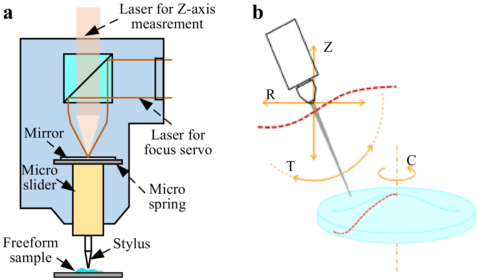
FFS optical element detection methods can be classified into contact and non-contact methods30. The contact detection method adopts point-by-point scanning, and the representative methods are the coordinate measurement machine and contour-meter method. Among these methods, the contact contourist UA3P45 developed by Panasonic (Japan) and the non-contact interferometer LUPHO Scan46 developed by Taylor Hobson (UK) are commonly used. Fig. 5a shows a schematic of the basic principle of contact contourist UA3P. When it is used for AS and FFS measurements, the surface shape measurement precision can reach 0.1 microns, which is suitable for high-precision lens measurements. However, the measurement speed becomes very slow when the lens aperture is large; therefore, it is generally suitable for the measurement of AS/FFS lenses with small apertures. As the lens aperture for AR-HMD is relatively small, the measurement requirements can be satisfied; this is the mainstream method for measuring the surface shape of AS and FFS. As shown in Fig. 5b, the non-contact interferometer LUPHO Scan, developed by Taylor Hobson (UK), adopts multi-wavelength interferometry to detect the surface of freeform optical elements. While the measurement time is shorter and the precision is higher, it is more expensive.
-
A geometrical waveguide is a lens structure composed of a series of transparent thin plates, and it has the advantages of being slim and lightweight. The rays coupling process of the geometrical waveguide is accomplished using a reflective mirror or a refractive prism. A beam-splitting array is used to couple the rays out. As shown in Fig. 6a, the geometrical waveguide display is composed of three parts: a microdisplay, projection optics, and geometrical waveguide optics. A waveguide is applied as a pupil expander to these three parts to reduce the thickness of the HMD47. The high-resolution image source provided by the microdisplay is converged by the projection optics to the entrance mirror in the waveguide. This ensures that the rays are continuously reflected on the substrate because of the TIR condition. The rays reach the partially reflective mirror array (PRMA), which sends them to the human eyes.
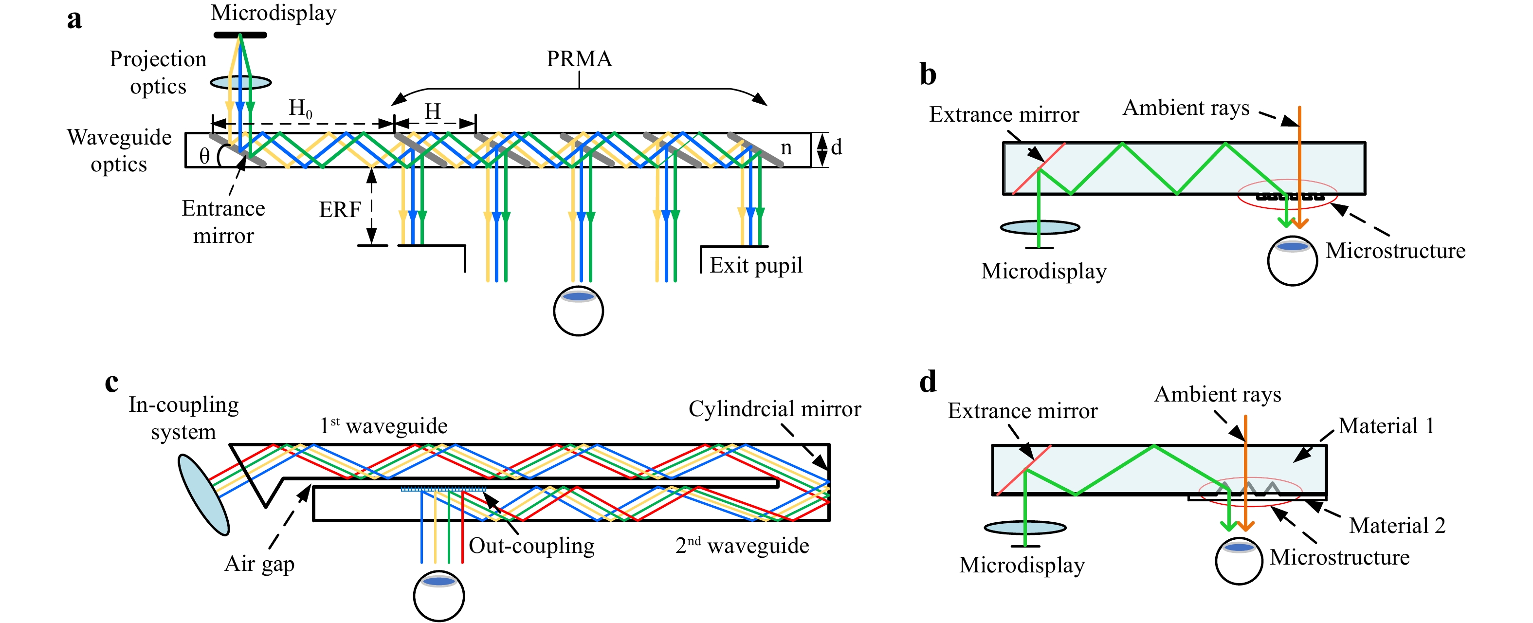
Fig. 6
a Composition of the geometrical waveguide display; b internal optical path of the double geometrical waveguide system; c optical path of the geometric waveguide with stepped structure; d optical path of the geometric waveguide with a triangular microstructure.Through research on geometrical waveguides, designers have made advancements in the optical structure of geometrical waveguide displays. Geometrical waveguides with deformed structures have also emerged. Yang and Twardowski developed a large FOV near-eye optical system with two geometrical waveguides48. Fig. 6b shows the internal optical path of the system. The rays provided by the microdisplay are coupled into the first waveguide through the projection system and spread into the first waveguide when reaching the cylindrical mirror, which is located at the end of the geometrical waveguide. Subsequently, the cylindrical mirror reflects the rays and couples them into the second waveguide. Through holograms or cascade mirrors, rays are coupled out of the second waveguide and received by the human eye. Hung and Pan applied a geometrical waveguide with a stepped structure to the design of an HMD system49. The basic schematic is shown in Fig. 6c. The rays coupled into the waveguide are continuously reflected through TIR conditions. When the rays approach the stepped microstructure, they are projected to the human eyes through TIR to increase energy efficiency. Based on the concept of a stepped structure, Zhao and Pan further deformed the microstepped structure into a triangular microstructure; this improved the energy efficiency while reducing processing difficulty50. The optical path is shown in Fig. 6d. To ensure that the rays are reflected at the position of the triangular microstructure (by the TIR), the index of refraction for material 1 should be lower than that of material 2 in the triangular microstructure.
The geometrical waveguide has five key parameters: (1) thickness; (2) the index of refraction for the glass material; (3) the angle between the entrance mirror and waveguide substrate; by selecting a suitable θ, stray light can be effectively eliminated; (4) the distance between the central point of the entrance mirror and that of the first mirror in PRMA; (5) the distance between two adjacent mirrors in PRMA. The mirrors in the PRMA are equally spaced and placed in parallel.
The waveguide processing method is shown in Fig. 7. Six parallel glass plates of different thicknesses are cemented together after coating. The cemented glass plates are tilted at a certain angle for position cutting, and each piece are set to the same thickness. Subsequently, the waveguide is rotated 90° to perform lateral cutting. Similarly, the dimensions are kept the same. Finally, the waveguide is edge-polished to form a waveguide without inclined corners.
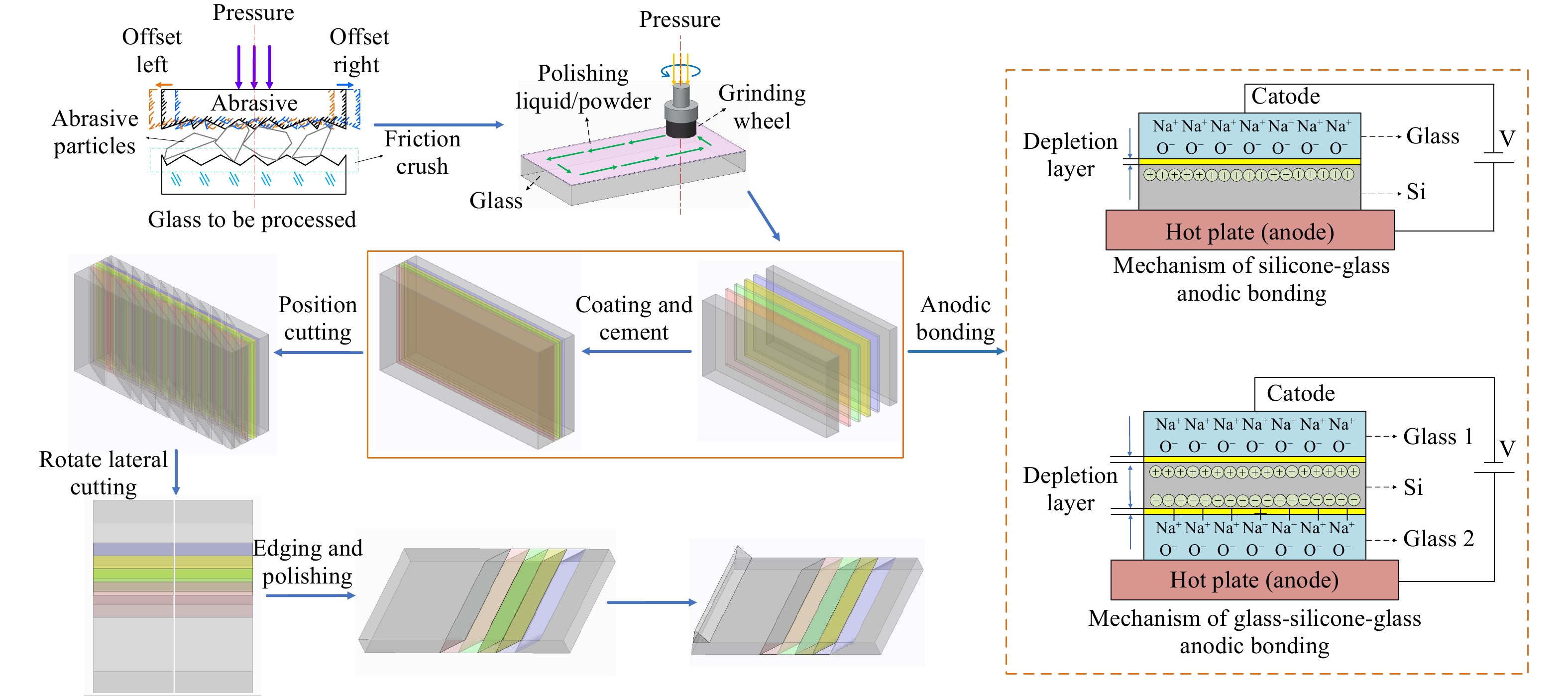
Fig. 7 Waveguide processing flow chart and anode bonding process.
The cementing of the glass plates is achieved through an anodic bonding process (Fig. 1c). Anode bonding is an electrical and thermal process that frequently bonds silicon wafers to glass substrates. With a bonding temperature of 320–360 °C, a bonding voltage of 600–800 V, and a bonding time of 15 min, the silicon-glass bonding area of more than 95% can be obtained. Moreover, for the anodic bonding mechanism, part of the voltage applied by the anodic bonding of the SiO2 intermediate layer is used to generate an electrostatic force to cause the glass and the silicon surface to react highly, forming a solid chemical bond; thus, the silicon-glass can be closely attached. The other part is exhausted in the SiO2 membrane.
Geometrical waveguide technology has many advantages, such as achieving high resolution, full-color display, ultra-thin thickness, wide FOV, and a large EPD51. Companies such as Lumus52, Epson53, and Optinven54 have developed products using geometrical waveguides. Although geometrical waveguides have apparent advantages over other perspective technologies, some problems remain to be solved. The main problems in geometrical waveguide HMDs are ghost stray rays and double imaging problems, which severely reduce the display quality55.
-
The diffractive optical waveguide is based on the physical structure of the grating, which is a microoptical solution. Through the use of diffraction and TIR conditions of light, the far-field light is transmitted to the near eye and projected to the external environment to fuse the image and external environment56. During the propagation of light in the waveguide, the incident angle of light entering the waveguide should be larger than the critical angle to ensure that the light is fully reflected in the waveguide before it reaches the human eye.
Generally, a diffractive optical waveguide system is composed of an image display source, a projection collimating optical system, and a planar waveguide element that integrates an in-coupling grating and an out-coupling grating57. As shown in Fig. 8, after the projection optical system collimates the light emitted by the image display source into parallel light, the diffraction light is propagated in the waveguide, satisfying the TIR condition via the in-coupling grating. After several iterations of TIR, the light is diffracted out of the waveguide through the coupling grating and into the human eye.
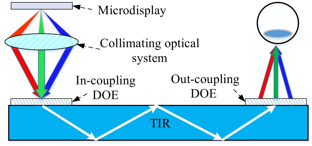
Fig. 8 Configuration of the planar waveguide display.
The grating used in the plane diffractive optical waveguide has a periodic structure. Depending on the different periodic structural forms, the planar diffractive waveguides are primarily divided into three types: SRG, VHG, and PVG waveguides. The following sections discuss the performance of the three types of grating waveguides.
-
The diffraction gratings used in planar diffraction waveguides generally adopt one-dimensional (1D) gratings with periodic structures in one direction and an infinite extension in the other.
The modulated light propagates in the waveguide along different orders of the grating, and its propagation angle is determined by the grating equation58,59. The diffraction efficiency of the grating can be calculated using rigorous coupled wave analysis (RCWA)60−62, and it can be realized by optimizing structural parameters such as the groove depth and tilt angle of the grating.
As shown in Fig. 9a, the basic structure of a general 1D binary rectangular grating includes the period, groove depth, and duty cycle. The binary rectangular grating was first used as a binocular VR display designed by NOKIA63. As shown in Fig. 9b, the collimated beam is diffracted by the in-coupling grating and propagated by TIR in two symmetric directions. It finally exits through the out-coupling grating and is received by the left and right eyes. The slanted surface relief grating breaks the symmetry of the grating and achieves a high diffraction efficiency in a specific order. Fig. 9c shows a commonly used slanted surface relief grating, in which the binary rectangular grating groove deviates from the normal line at a certain angle. In addition to considering the grating period, the groove depth, duty cycle, and tilt angle must be determined in the design.
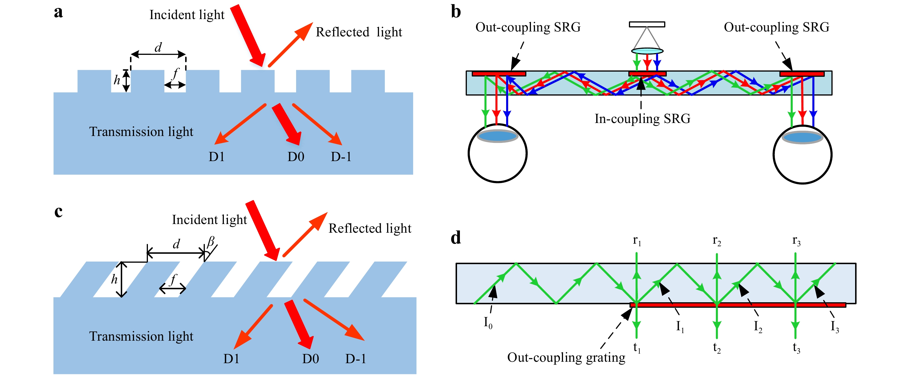
Fig. 9 1D grating and waveguide structure.
a schematic of rectangular grating structure; b binocular diffraction waveguide structure; c schematic of a slanted grating structure; d schematic of one-dimensional pupil expansion.In the actual application process, the eye should have a certain movement-observation distance. An exit pupil expansion is required at the exit coupling end to expand the eyebox to guarantee that the eye can perceive the complete image when moving along the direction of light propagation in the waveguide. As shown in Fig. 9d, to realize exit pupil expansion, the out-coupling diffraction grating elements should be designed precisely. When the light hits the out-coupling grating element, part of the light is diffracted out of the waveguide. The remainder of the light will continue to be totally reflected. Each time the TIR light interacts with the out-coupling grating, diffracted light is emitted. The exit pupil expands in one dimension along the TIR light's travel direction.
When a single-layer diffractive waveguide is used to achieve a full-color display, the TIR of red–green–blue (RGB) light in the waveguide should be within the acceptable range, while the FOV of red light will be limited to a lower range. To achieve a full-color display, other methods must be considered to expand the FOV of the color waveguide. One method of achieving this is to stack grating waveguides with different periods to accommodate different light waves, thus increasing the FOV of the waveguide. As shown in Fig. 10a, the Nokia Research Center used a two-layer waveguide stack structure62. The grating period of the lower plate is smaller than that of the upper plate; one layer is used for red wavelengths and the other for blue and green wavelengths. Fig. 10b shows the three-layer waveguide stack structure of the Microsoft HoloLens64. Each waveguide layer has a different SRG grating period to propagate different colored lights. Another method is to divide the exit pupil expansion (EPE) function into two separate parts. One plate is used to cover the positive incident angle and the other to cover the negative incident angle. As shown in Fig. 10c65, this can be achieved by selecting different grating periods.
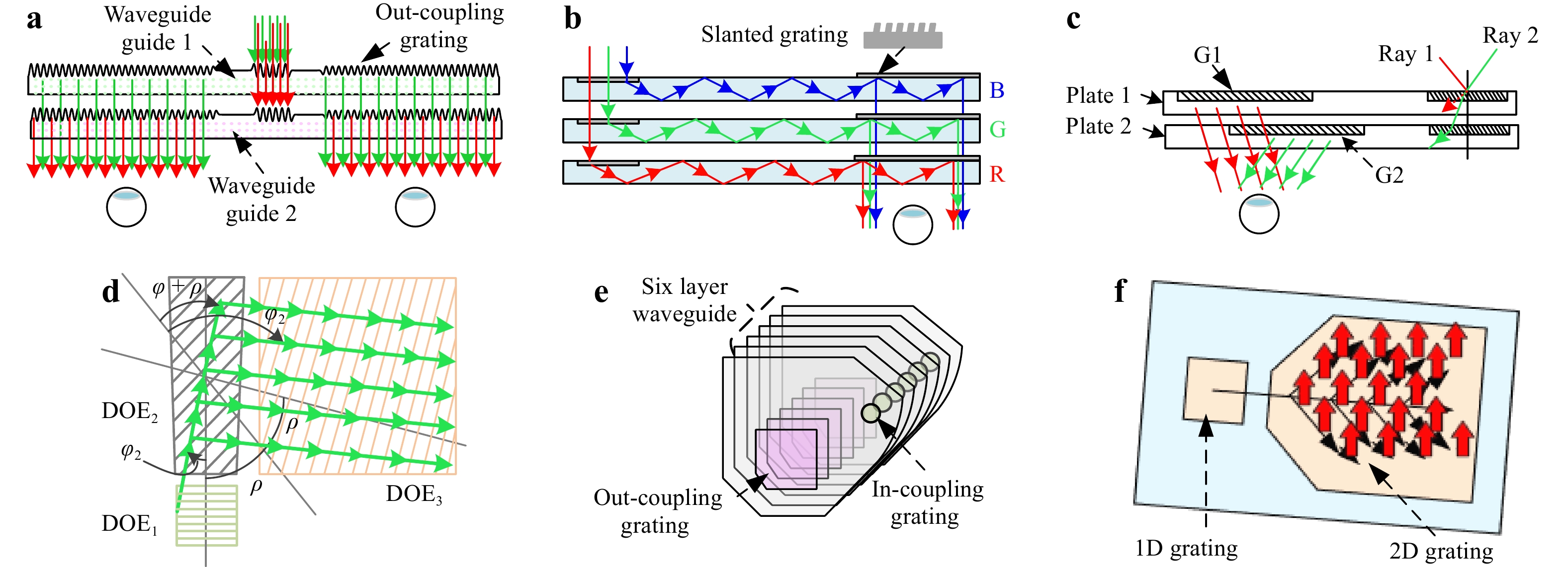
Fig. 10 Multilayer waveguide stack structure and 2D EPE.
a double-layer waveguide stack structure; b RGB three-layer color waveguide; c operating principle of the 1D EPE with a large FOV; d schematic of 2D EPE; e six-layer SRG waveguide superposition to achieve multi-focal plane; f pupil expansion using 2D grating SRG waveguide.To increase the size of the eyebox, scholars have proposed a two-dimensional (2D) EPE structure (Fig. 10d)63,66,67. In 2D EPEs, a redirection grating (DOE2) is required. When the light beam propagates to DOE2, the light beam continuously contacts DOE2 and is transformed from 1D propagation to 2D beam propagation. As the figure shows, the beam expands vertically before reaching DOE3. After DOE3 diffraction, the horizontal direction also expands, finally forming a 2D beam band.
The 2D EPE structure was applied to the diffractive waveguides produced by Microsoft and DigiLens33,64,68. The optical module of the HoloLens one-generation system adopts a three-layer waveguide stack structure to accommodate RGB light and has a diagonal FOV of 35°. The second-generation optical module used a two-layer waveguide stack with a diagonal FOV of 50°. It was a significant improvement over first-generation FOV.
For these near-eye display solutions, the focus cues that the virtual scene can provide to the human eye are inadequate. As shown in Fig. 10e, to address the vergence-accommodation conflict (VAC), Magic Leap created different focal planes by stacking six SRG waveguides, each dedicated to one color wavelength (red, blue, or green)70. Among them, three layers render near-focus vision, and the other three layers render far-focus content. They are then distributed on two different focal planes, thereby improving the comfort of human eyes when viewing images.
In addition to 1D grating waveguides, the function of planar waveguides can be realized using 2D gratings. The subwavelength grating structure has different periodic structures in two directions. As shown in Fig. 10f, to satisfy the requirement of 2D EPE, the out-coupling grating is a 2D grating that utilizes the duplication of the pupil in two directions. This technology has been applied to optical waveguide display technology developed by WaveOptics71.
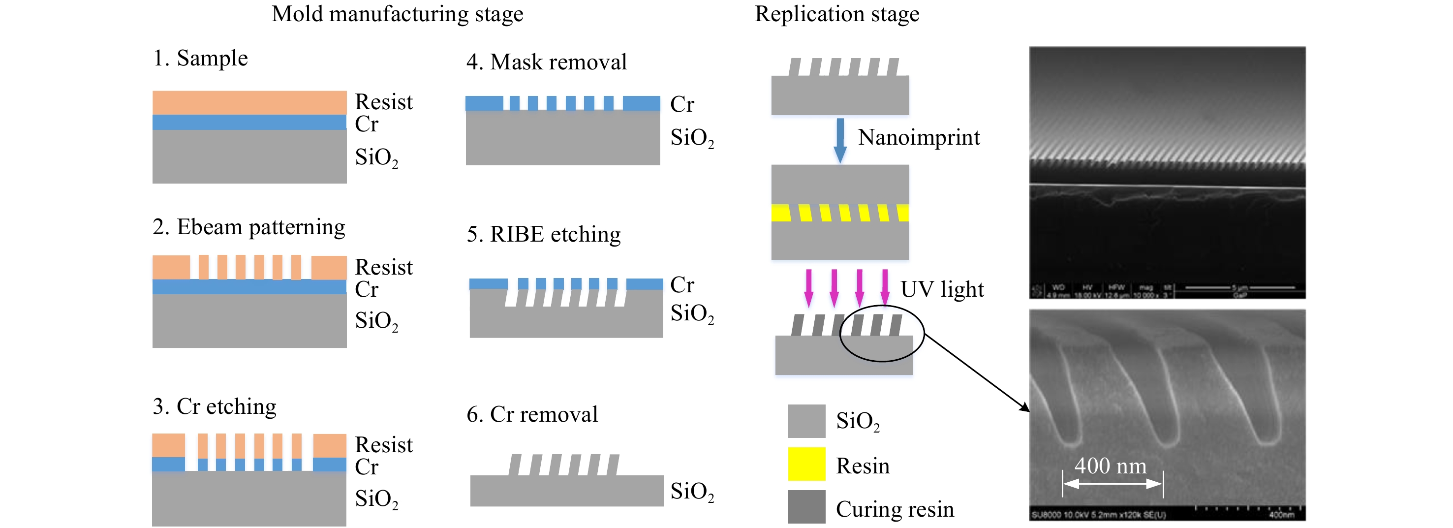
Surface relief gratings can be manufactured through focused-ion beam manufacturing72−74 or reactive-ion etching (RIE) and e-beam lithography (EBL)75. This processing technology is shown in Fig. 11. Using SiO2 as the substrate, a chrome layer (Cr) and a resist layer are coated onto the substrate. The process can also begin with an EBL to generate the grating pattern. The resist layer is then transferred into the Cr metal layer using a chlorine dry etching process. Thereafter, the resist layer is removed using the oxygen plasma process, and the Cr layer is used as an etching mask for reactive-ion beam etching (RIBE). During RIBE etching, the ionized argon beams are oriented to the substrate at an oblique incident angle. When the curtain etching depth is achieved, the Cr metal layer is removed through chemical wet etching32.
Nanoimprint lithography (NIL)76 is the most applied method of mass-producing AR diffraction gratings. First, the slanted grating master must be treated through an anti-adhesion treatment. For a lower defect level and higher patterning efficiency, the intermediate pattern stamp (IPS) process was invented for pattern transfer77. It uses a polymer film as intermediate stamp for the pattern transfer. This has created opportunities for the use of NIL technology in industrial applications. Today, most plate-to-plate NIL processes used in the industry have adopted the polymer stamp as an intermediate template to create the final duplication on the target substrate.
More details of the IPS process are shown in Fig. 11. Using the NIL templates, a polymer film is applied for the NIL process. The NIL template structure is transferred to the polymer film, resulting in a soft polymer stamp (IPS, Fig. 11). Using the IPS as an NIL template, a high-RI resist layer is imprinted. After these two steps of the NIL process, the pattern on the high-RI resist layers have the same orientation as the original NIL template.
Some problems that affect the further application of SRG remain to be solved. In terms of design, diffraction waveguides have large angles and wavelength selectivities and are prone to dispersion problems, which can result in uneven color of the exit pupil and produce a rainbow effect. Moreover, there are other higher diffraction orders in the diffraction grating, and the higher-order diffraction light will exhibit a light leakage phenomenon outside the optical waveguide. In terms of processing technology, the angle of the slanted grating should not be excessively large, and the ratio of the line width to the depth should not be excessively small for the production of SRG. Otherwise, because of the limitation of Young's modulus in the nanoimprint stage, the excessively long structure will be unable to support its morphology. This will result in the direct collapse of the imprint grating. EBL exposure instruments for fabrication equipment with reliable accuracy and speed are expensive and require a specialized ultra-clean environment.
-
The VHG waveguide system is another solution for light waveguides78,79. The VHG is a 3D structure with a periodic refractive index based on the principle of interference. Theoretically, the diffraction efficiency can reach almost 100% when the Bragg condition is matched. The diffraction efficiency decreases with the angle of deviation80. The VHG is divided into two types: reflective and transmissive. Reflection volume holograms are widely employed in the field of waveguides. In 1969, Kognik proposed the coupled wave theory for the analysis of the diffraction characteristics of VHG81,82. In 1989, Amitai et al. proposed the application of hologram diffractive elements to HMD15,83.
Since 2007, the British BAE Systems company has been committed to the research and development of the Q-sight series of waveguide products84, and they introduced transmissive hologram gratings into their HMD designs. When the light is totally reflected in the glass substrate, it is diffracted as it hits the holographic surface. The diffracted light no longer satisfies the condition of total reflection, and is emitted from the glass plate. Additionally, the entrance pupil size can be adjusted to achieve continuity of the light exit region (Fig. 12a).
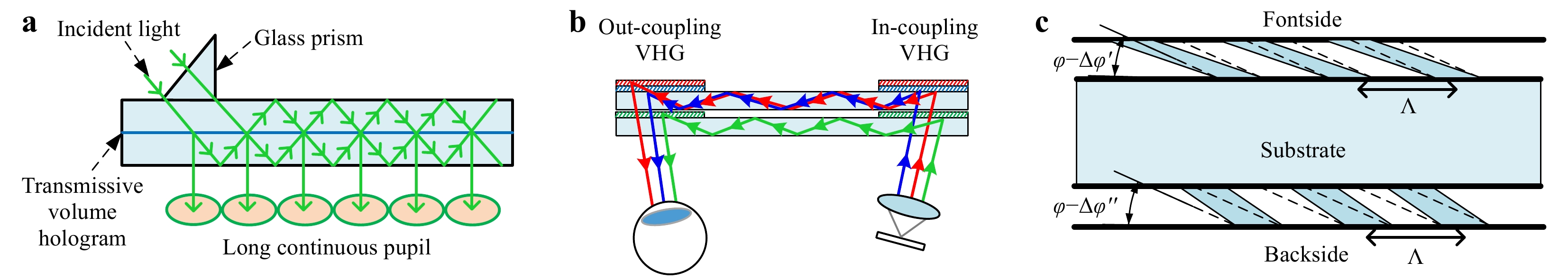
Fig. 12
a Optimized holographic optical waveguide from BAE Systems (one axis shown); b schematic of a full-color VHG waveguide with oblique optical axis from Sony; c schematic of a VHG waveguide with deviation mirror-striped structure.In 2008, Sony developed a full-color waveguide display through multiple holographic layer superposition85. The waveguide includes in-coupling and out-coupling reflection volume hologram stacks. However, these multiple holographic layer superpositions can cause stray light because the gratings of every hologram layer are different. Consequently, they tilt the optical axis of the display and collimator by 10° relative to the coupled in-hologram (Fig. 12b). Thus, the Bragg λ parallax between the two ends of the FOV decreases from 45 to 37 nm, and the color gamut increases from 76% to 120%. In 2015, they developed a double-sided coupled holographic optical element (HOE) with a slight deviation from the ideal mirror-striped structure (Fig. 12c). Thus, they can obtain a brightness that is three times higher without losing uniformity, and the FOV increases up to 19×6°86.
Consumers are not only satisfied with the non-chromatic aberration and uniformity of images, but also hope to obtain light and compact AR products. In 2018, Sony began to use resin materials to replace traditional glass substrates, which significantly reduced the weight of their devices87. The next section introduces the production process of the VHG waveguide.
Volume holograms are formed by the laser exposure of photosensitive materials. Photopolymers are the most used media materials today. Compared with traditional silver halide emulsions, the resolution rate of the holograms produced with photopolymers is high and can be stored for a long time88−90. The reflection volume holograms that record the optical path diagram are shown in Fig. 13a. During exposure, the laser emits light, which passes through the beam splitter and is then divided into beams with a certain light intensity ratio. After light is collimated by the expanding beam, it is projected on both sides of the holographic dry plate pre-coated with a photoresist layer.
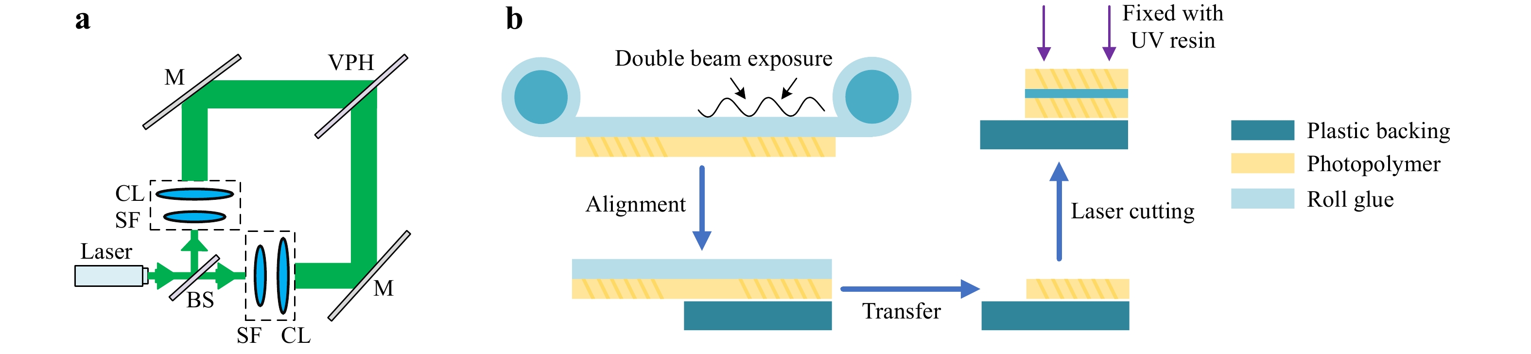
Fig. 13
a Schematic of reflective VHG recording process; b Schematic of roll-to-roll process for plastic holographic waveguides92.The hologram exposure process is similar, but the waveguide manufacturing process is different91. In 2018, Sony developed a lightweight waveguide processing technology that replaced traditional glass substrates with resin materials87,92,93. Fig. 13b shows a new roll-to-roll process for plastic holographic waveguides. First, the HOE is formed on the photopolymer film using a two-beam interferometric exposure method. Second, the plastic sheet is obtained through injection molding. The parallelism and thickness tolerances of the plates are firmly controlled. Thereafter, the HOE film is attached to the plastic waveguide using the HOE lamination process. Next, during the stamping process, the plastic holographic waveguide is cut into a specified pattern. Finally, during the color matching process, the inclination of the red and blue plastic waveguides is adjusted to the green plastic waveguides, which are fixed with UV resin92.
Compared with SRG and geometric waveguides, VHG waveguides have lower research and developmental costs and faster production. The production of VHG waveguides is limited by many challenges, such as the production of holographic materials. Most manufacturers now use photopolymer materials as the media material, but the properties of different materials are also different, which directly affects the uniformity of the coating, the FOV of the waveguide, and other optical properties92. Furthermore, the environmental stability requirements during the exposure and production of holographic waveguides are very strict. Humidity, temperature, and air fluidity affect exposure. Moreover, owing to the limitations of the holographic waveguide, it is difficult to increase the FOV of the holographic waveguide85.
-
Pancharatnam–Berry phase optical elements (PBOEs) are emerging LC-based planar structures that are similar to cycloidal diffractive waveplates (CDWs). Several useful optical effects have been realized using PBOEs, such as focusing, wavelength selection and waveguide coupling. Because of their prominent behavior in optical tunability, polarization selectivity, and diffraction efficiency, PBOEs have potential widespread applications in emerging display systems94,95. Compared with VHG, the CDW has polarization sensitivity, and a high diffraction efficiency can be achieved when the polarization handedness of the incident beam is matched96−100. However, owing to the limitation of the physical mechanisms, the diffraction angle of CDW is frequently small (approximately 15° in air)96,100. In recent years, PVG has been proposed to combine the advantages of VHG and CDWs, which are thinner than traditional VHG, and is several tens of microns thick34,35,101. Compared with VHG, where the modulation of the refractive index is in the order of 10−2, the PVG is significantly higher (0.2 is the most common)34. Theoretically, an arbitrary diffraction angle can be achieved by controlling the period size along the x- and y-directions. The diffraction efficiency and spectral bandwidth of PVG are basically independent of the diffraction angle, and the angular bandwidth is significantly larger than that of VHG, which are beneficial to increasing the FOV in AR-HMDs. In addition, a larger PVG thickness results in a higher diffraction efficiency. As a result, PVG exhibits a good combination of CDW and VHG: large diffraction angle, high diffraction efficiency, and polarization selectivity. Similar to VHG, PVG can be formed into transmission and reflective types, and the reflective type is used in AR-HMDs.
Weng34 proposed a method of constructing a high-efficiency PVG physical structure with a large diffraction angle. The basic physical principle of the PVG is shown in Fig. 14a. In the PVG, the rotation angle of the LC optical axis on the x–z plane is formed by using the top substrate, and it changes continuously and periodically along the x-axis. Beneath the top substrate of the PVG, the LC exhibits a helical structure with a period length along the y-axis. This method produces many periodic and slant refractive index surfaces (the dotted green line in the diagram). By doping the chiral dopant, the spiral structure along the y-direction can be conveniently realized, and the periodicity can be controlled by adjusting the helical twist power and concentration. Fig. 14b shows the operating status of the reflective PVG. First-order polarization preserves the same handedness as the incident beam. In addition, when the incident beam is orthogonal to the rotation direction of the PVG, it will not change the polarization state and will be transmitted in the 0th order. Fig. 14c shows the optical path diagram of the PVG waveguide AR-HMD. Two PVGs with right- and left-handedness are stacked as in-coupled gratings. The in-coupled gratings diffract the right and left circularly polarized beams and transmit another orthogonally polarized beam. Owing to the orthogonal handedness of these two PVGs, the diffraction angles are opposite each other. The image of the microdisplay is transmitted in the waveguide because the diffraction angle is larger than the TIR angle. Two reflective PVGs are mirrored symmetrically and embedded in the waveguide as out-coupled gratings. The propagating image is finally diffracted and separately output to the human eye through the two out-coupled gratings.
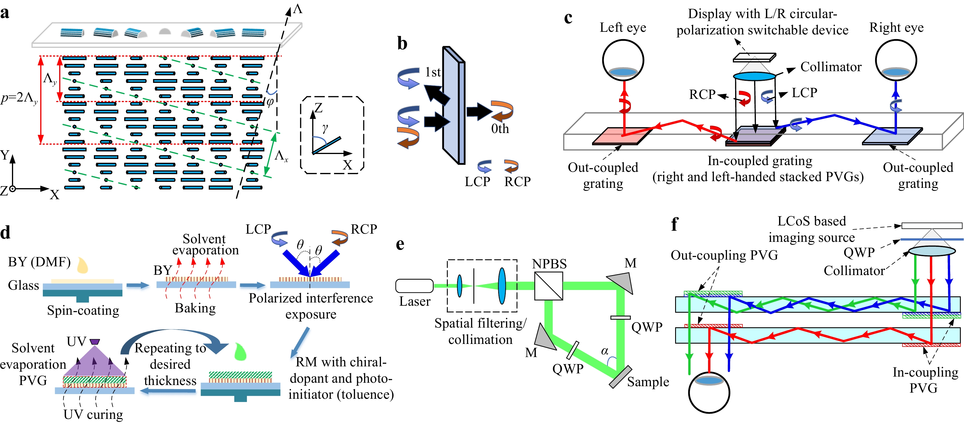
Fig. 14
a Basic physical principle of PVGs; b operating status of reflective PVG; c optical path diagram of PVG waveguide AR-HMD; d flowchart for fabricating PVGs; e schematic diagram of optical path for PVG exposure; f PVGs used as couplers in different waveguide layers for different spectra.Fig. 14d shows the flowchart of fabricating the PVGs. Before the exposure fabrication process, the brilliant yellow (BY) is dissolved in the dimethylformamide (DMF) and spin-coated on a glass base to obtain uniform and thin films. The films are then dried on a hotplate101,102. Subsequently, the film samples are exposed to polarized interference. In addition, a reactive mesogen with a chiral dopant and photo-initiator are included when spin-coating. The coated films are then cured using UV light. Finally, they are repeatedly coated and cured until a sufficient thickness is achieved. Fig. 14e shows a schematic of the optical path of the PVG exposure. The beam of the linearly polarized He–Cr laser passes through an unpolarized beam splitter and is divided into two paths. Subsequently, the two splitter beams pass through two quarter-wave plates (QWPs) to generate two opposite-handed circularly polarized beams. These two beams are aligned to create an angle α onto the coated substrate to generate periodicity. As shown in Fig. 14f, Zhang et al.102 developed a double-layer PVG-coupling waveguide, which realized a full-color AR-HMD with a diagonal FOV of 35°. The PVG-coupling waveguide exhibited a diffraction efficiency of over 80% in the spectra of red (630 nm), green (532 nm), and blue (457 nm).
The PVG is the latest structure with polarization-selective gratings, and it can easily achieve diffraction efficiencies higher than 80% (the greater the PVG thickness, the higher the diffraction efficiency), which cannot be achieved using other raster grating waveguides. The large diffraction angle can be controlled by adjusting the arrangement period of the LC microstructure in the x- and y-directions. In addition, the angular bandwidth of the PVGs is significantly wider than that of the VHGs. Furthermore, the light transmittance is higher than 50%, which is an important advantage for the realization of a large FOV in the future. However, the current research is only being conducted under laboratory conditions, and the complex exposure preparation process still makes it difficult to mass produce for the commercial market.
-
Metasurfaces are nanooptical elements that can arbitrarily tailor the fundamental properties of light within ultrashort distances. They can be used in applications such as beam shaping, anomalous refraction, holography, and metalens development36,103−109. A metalens is one of the most ideal imaging application devices, and its application in imaging research has also attracted significant interest globally105. Metalenses have the advantage of a large NA, ultra-thin shape factor, and versatility. Lee et al.36 first proposed a method of near-eye displays using metalenses and successfully developed a principle prototype. To realize a transmission large-NA eyepiece, large area, and wide FOV, they designed a dielectric metasurface with a subwavelength-scale microstructure with arbitrarily engineered anisotropy. The cell structure of the metalens is shown in Fig. 15a. A metalens can be formed by arranging many nanorod units on SiO2 according to a certain position and azimuth (Fig. 15b). Considering the unique characteristics of the nanorod, the transmittance amplitudes of co-polarized and cross-polarized can be controlled independently using the structural arguments of the nanorod, which is important for the realization of AR imaging.
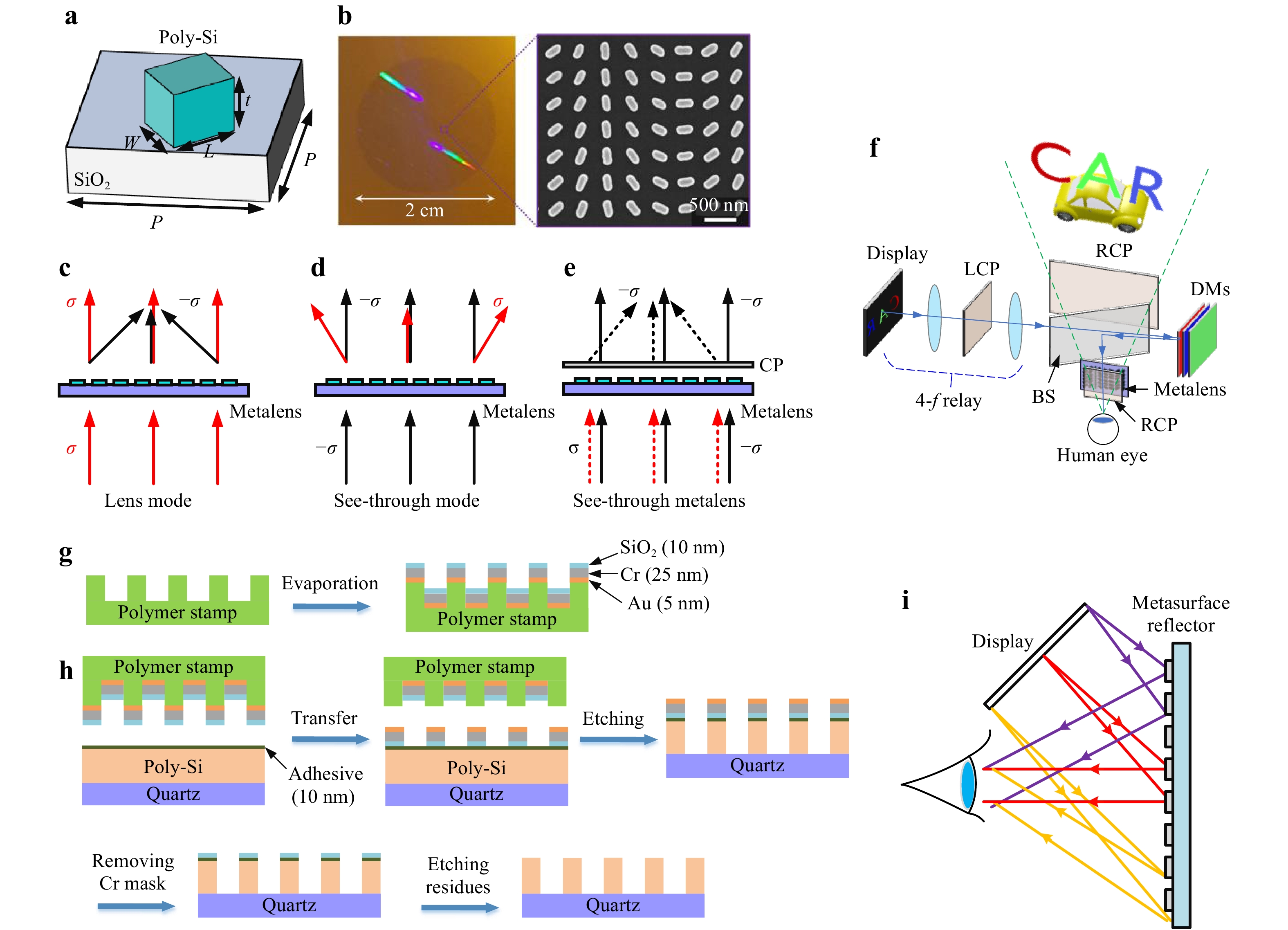
Fig. 15
a Unit cell structure of a metalens; b metalens element36; c–e optical behavior when different circularly polarized lights are projected on the metalens; f optical path diagram of the metalens-based optical-imaging system; g–h schematics representing the fabrication process of the proposed metasurface based on nanoimprint; i HMD solution based on metasurface reflector.To design a metalens with an equivalent focal length f, the structure of each nanorod is designed by encoding the space phase distribution. The device behaves optically as a transparent glass in the co-polarized transmission mode and as a lens in the cross-polarization mode. The final optical behavior of the metalens is shown in Fig. 15c−e. For incident light with a handedness σ, the device is equivalent to a convex lens for cross-polarized light and to the common transparent glass for co-polarized light. For incident light with a handedness −σ, the device is equivalent to a concave lens for cross-polarized light and to the common transparent glass for co-polarized light. By using a circular polarizer to block light with the handedness −σ, the concentrated light and direct transmitted light remain: incident light converges with the handedness σ, while the opposite-handedness component transmits the light. AR imaging is realized through the above-mentioned basic principles, where the handedness of virtual information is σ and the handedness of light from the real scene is −σ. The optical path diagram of the AR-HMD optical-imaging system is shown in Fig. 15f. After the light from the display passes through the 4-f relay system, which contains the left circular polarizer, it passes through the beam splitter (BS) to the three dichroic mirrors (DMs) for reflection. It is then reflected by the BS through the metalens and right circular polarizer, entering the human eye to form a virtual image. In the principal prototype, DMs are used to realize achromatic behavior by changing the imaging position of different wavelengths. The prototype with a metalens aperture of 20 mm achieved an FOV of 90° for a monochrome display and 76° for a full-color display. In addition, the co-polarized transmission efficiencies of the prototype reached 79% in the spectra of the red, green, and blue regions.
Metalens optical elements with a large size (diameter: 20 mm) and high NA (0.61) are developed based on nanoimprinting precision machining technology36. As shown in Fig. 15g–h, the overall process involves two steps: Using a standard electron beam lithography process, a polymer stamp with a metasurface pattern is prepared to be applied to the nanoimprint (Fig. 15g). Several films are then evaporated using an electron-beam evaporator. For the target sample, a quartz wafer with a poly-Si film and adhesive layer is prepared using low-pressure chemical vapor deposition and spin coating (Fig. 15h). Using the prepared polymer stamp, the metasurface patterns of the Au, Cr, and SiO2 films are transferred to the wafer. The sample is then etched using Au and Cr patterns as a hard mask. After removing the Cr mask and other residues by the Cr etchant and etching further, the sample is finally produced. Although the resolution of nanostructures fabricated using nanoimprinting is lower than that of nanostructures manufactured using EBL, they are sufficient and effective. In addition, nanoimprinting technology can be used to achieve mass production, which is beneficial for the AR market.
In summary, Lee et al. overcame the constraints of large traditional optical elements. They developed a metalens-based AR-HMD prototype, which realized an ultra-wide FOV and full-color imaging with a large eyebox. However, three dichroic mirrors were included in the prototype to correct the inherent chromatism from the metalens, thus increasing the complexity and weight of the system. Therefore, to achieve a better application of metalenses in AR-HMDs, the correction of metalens chromatic aberration should be studied106−109. In addition, as shown in Fig. 15i, an AR-HMD solution based on a subwavelength patterned reflector of a metalens visor was proposed by Hong et.al37. Theirs was the first study to explore the possibility of using metasurfaces to create compact near-eye reflector visors. The metalens visor is similar to the off-axis first-order FFS reflective optical solution because the combiners are all monolithic combiner structures, and they are frequently easily obtain a larger FOV. The metalens visor achieved higher imaging quality with a wider FOV of 77.3° in the horizontal and vertical directions. The size of the system was only 4 cm × 4 cm. The MTF of the metalens visor was over 30% at 33 cycles/mm and the imaging distortion was less than 8.76%. In addition, the reflection surface adopted in this solution was planar and had a more compact structure than the traditional off-axis first-order FFS reflective optical solution. Compared with the large distortion introduced by the traditional off-axis first-order FFS reflective structure, the metalens visor solution introduced only a small optical imaging distortion (<8%). However, because the pre-distortion of image distortion correction was small, the effective pixel of the microdisplay improved; therefore, the overall resolution of the final image improved. However, they only achieved the design and simulation verification and did not create the principle prototype and discuss the feasibility of the project according to the design. Therefore, it was difficult to determine the actual imaging quality, diffraction efficiency, transmittance, and stray light suppression of the system, because these are also the common concerns of current AR-HMD systems based on microoptics and nanooptics.
-
Table 1 compares the different AR-HMD optical combiners. Each has advantages and disadvantages. Based on the optical effect, compared with micro and nanooptics, macrooptics can achieve a higher optical efficiency and a larger FOV. A larger FOV can provide a more immersive experience for customers. The development of high-precision diamond turning and optical injection processing technologies facilitated a submicron machining precision and guaranteed the mass production of AS and FFS lenses. For AS and FFS lenses with small apertures, the submicron machining accuracy is sufficient to satisfy current AR-HMD requirements. However, the detection of AS and FFS still has some limitations, which are limited detection accuracy and speed. The polishing, coating, and cementing processes of geometrical waveguides also interfere with the quality of the geometrical waveguide, because it requires a parallelism of PRMA less than 10”. In terms of the shape factor, the optical combiners of macrooptics are larger than those of micro and nanooptics. AR-HMDs based on combiners of macrooptics still have the problem of being bulky and heavy.
Type Combiner Efficiency Bandwidth FOV (diagonal) Form factor Fabrication requirements Macrooptics Traditional <50% Large 90° Large CNC grinding; diamond turning and injection
(submicron machining precision)FFS prism <50% Large 120° Large Geometrical waveguide <20% Large 40° Medium Polishing, coating, cementing. (Parallelism of PRMA<10’’) Microoptics SRG <10% Medium 56° Small RIE and EBL; nanoimprinting. (machining precision <100 nm) VHG <10% Small 40° Small Laser exposure; (submicron machining precision) PVG <10% Medium 50° Small Nanooptics Metalens <10% Medium 76° Small RIE and EBL; nanoimprinting. (machining precision <100 nm) Metasurface reflector — Medium 81° Small Table 1. Comparisons among AR-HMD Optical Combiners
Compared with macrooptics, because the diffraction effect can result in a larger beam deflection angle, combiners based on microoptics are small in size and weight, making them easy to miniaturize. An acceptable FOV larger than 40° can be realized in some aspects. The bandwidth for SRG and PVG are medium, and small for VHG. However, the current microoptics-based diffraction waveguide combiners still encounter many problems such as low efficiency (<10%), chromatic aberration in full-color displays, illuminance nonuniformity, and lack of mass production processing technology, which hinder their commercial application. Furthermore, owing to the large angle and wavelength selectivity and the higher order diffraction light of the diffractive waveguide, the dispersion and stray light are prominent problems that disturb the user experience. RIE and EBL technologies are used to manufacture SRG, and the nanoimprinting process can realize a high-precision (machining precision < 100 nm) large-size and mass production. In EBL technologies, the spin-coated resist layer is first exposed by the electron beam and then etched to reduce its lateral size to generate the nanostructures. However, the angle of the slanted grating and the ratio of line width to depth must be strictly limited in the production of SRG to avoid the direct collapse of the imprint grating, which restricts and influences the optimal optical design effect. High cost and low efficiency are still problems that limit SRG. In the manufacturing of VHG and PVG, submicron machining precision can be achieved using the laser exposure method. The production of holographic materials directly affects the uniformity of the coating. Furthermore, environmental stability requirements, such as humidity, temperature, and air fluidity, affect the exposure quality. This type of exposure method makes it difficult to realize a mass production process that maintains quality, which hinders the popularization and application developments for the devices. The emergence of roll-to-roll production technology has significantly promoted the mass production of waveguides. However, owing to the limitation of the Bragg condition, the realization of full-color waveguide processing without chromatic aberration is still a significant challenge.
For nanooptical combiners, the combiners based on metalens facilitate a small form factor and large FOV. The nanooptics-based combiners achieve the imaging effect through the modulation of the phase and polarization using the arrangement of nanorods. The bandwidth for the metalens and metasurface reflectors is medium. However, the current nanooptics-based combiners have many problems such as low efficiency (<10%), chromatic aberration in full-color displays, and lack of mass production processing technology, which hinder their commercial application. Furthermore, owing to the large angle and wavelength selectivity, and the roughness of the device surface, dispersion problems are still prominent and disturb user experience. In the manufacturing of metalens or metasurface reflectors, because RIE and EBL technologies and the nanoimprint processes (machining precision <100 nm) are used, the problems encountered are similar to those of the SRG. The precision of the sub-structure nanorod contribute significantly to the final optical effect.
In the future, the improvement of the optical effect in the current combiners will depend on the advancement in the combination of various solutions, the manufacturing technologies, and the adoption of emerging materials and display devices.
Challenges and opportunities coexist for the design method, and the combination of various solutions will introduce complex methods and systems. However, this is a promising approach. FFS elements frequently exhibit continuous smooth and variable curvature characteristics and have a significant correcting effect on imaging aberration, which is beneficial to increasing image quality. The image quality of the system must be increased significantly by applying it to the projection system of waveguide-type combiners. Application examples include the combination of an FFS element with a geometric waveguide51 and an FFS element with a VHG diffraction waveguide110. In addition, AR-HMD solutions based on the combination of retinal projection (acquiring a large FOV) and SRG diffraction waveguide combiners (acquiring small form factor) have also received significant interest and applications69. In addition, multifocal imaging technology is promising for use in AR-HMDs to produce virtual patterns with multiple depths of virtual imaging or real stereoscopic effects111.
In manufacturing of microoptics and nanooptics in particular, the improvement of the optical effect still relies on sub-structure processing. Sub-structures with complex forms (increased freedom of design and feasibility of larger bandwidth) and high precision (satisfying design requirements) will result in better optical effects. The combiner fabrication of SRG and metalens is accomplished using semiconductor fabrication technology. Some problems remain, such as color inhomogeneity, the rainbow effect, and achieving an excellent fabrication rate. The improvement of the resolution and efficiency of EBL and laser exposure methods are expected to be central in the fabrication of micro and nanooptical combiners. Furthermore, we can expect to achieve low cost, large size, and mass production of micro and nanooptics based on advances in nanoimprint technologies. More time is required for manufacturing technologies to mature further and for the rate of mass production to increase.
The emergence and adoption of materials such as polymer nanomaterials will also assist in achieving a better optical effect, such as a decrease in optical chromatic aberration and better imaging quality. The VHG combiners also depend on exposure and substrate materials. From silver halide and dichromate to today's photoinduced polymer materials, the exposure effect of VHG has been significantly improved88−90. From traditional glass substrates to today's resin substrates, the lightweight and shape of the VHG waveguide system has improved87. These emerging microdisplays112 can be further studied to create specialized image sources, such as a special polarization and curved-screen displays.
-
In this review, we investigate recent developments and discuss the prospects of existing AR-HMD combiner optical solutions, which are divided into three categories: optical solutions based on macro-, micro-, and nanooptics. Macrooptical solutions based on Snell’s law of refraction and reflection have undergone a transformation from traditional optical solutions to freeform prisms and geometric optical waveguide solutions. They have significantly improved the imaging quality and compactness of AR-HMD systems significantly. The use of FFS effectively expands the FOV and reduces the use of traditional optical components. Planar optical waveguides further decrease the volume and weight of the system. The use of grating devices based on microoptical solutions makes AR-HMDs lighter and thinner. The planar diffractive waveguides use subwavelength gratings to achieve light coupling. The FOV and full-color display are also important factors that limit the development of diffractive waveguides. SRG waveguides must frequently be stacked into multiple layers to develop full-color displays, while VHG waveguides frequently require three-step multilayer exposure, which can easily cause color crosstalk, making it difficult to achieve a full-color display with a large FOV. The emergence of PVG combiners based on LC significantly increases the diffraction efficiency while expanding the FOV, which is the research direction of emerging AR-HMD combiners. For nanooptical solutions, metasurfaces have also been applied to AR-HMDs, and to an extent, the design of ultra-thin eyepieces with large FOVs and NAs has been realized. With the innovation of design methods, advances in manufacturing methods, and emerging materials and devices, AR-HMD optical solutions with the characteristics of prescription glasses may be developed in the near future.
Design and manufacture AR head-mounted displays: A review and outlook
-
Dewen Cheng1, 2,
 ,
, - Qiwei Wang1,
- Yue Liu1,
- Hailong Chen1,
- Dongwei Ni1,
- Ximeng Wang1,
- Cheng Yao1,
- Qichao Hou1,
- Weihong Hou2,
- Gang Luo3,
-
Yongtian Wang1, *, ,
- Light: Advanced Manufacturing 2, Article number: (2021)
- Received: 30 December 2020
- Revised: 30 August 2021
- Accepted: 31 August 2021 Published online: 26 September 2021
doi: https://doi.org/10.37188/lam.2021.024
Abstract: Augmented reality head-mounted displays (AR-HMDs) enable users to see real images of the outside world and visualize virtual information generated by a computer at any time and from any location, making them useful for various applications. The manufacture of AR-HMDs combines the fields of optical engineering, optical materials, optical coating, precision manufacturing, electronic science, computer science, physiology, ergonomics, etc. This paper primarily focuses on the optical engineering of AR-HMDs. Optical combiners and display devices are used to combine real-world and virtual-world objects that are visible to the human eye. In this review, existing AR-HMD optical solutions employed for optical combiners are divided into three categories: optical solutions based on macro-, micro-, and nanooptics. The physical principles, optical structure, performance parameters, and manufacturing process of different types of AR-HMD optical solutions are subsequently analyzed. Moreover, their advantages and disadvantages are investigated and evaluated. In addition, the bottlenecks and future development trends in the case of AR-HMD optical solutions are discussed.
Research Summary
Design and manufacturing of AR head-mounted display
Augmented reality head-mounted displays (AR-HMDs) not only enable users to visualize virtual information generated by a computer anytime and anywhere, but also enable users to see real images of the outside world. In the AR-HMDs, optical combiners and display devices are used to mix objects in the real world and the virtual world, which are perceived by the human eye. The team of Yongtian Wang from Beijing Institute of Technology divided the AR-HMD optical solutions for optical combiners into three categories: optical solutions based on macro optics, micro optics and nano optics solutions. The team analyzes the physical principles, optical structure, performance parameters, and manufacturing process of different types of AR-HMD solutions, and they also evaluate their advantages and disadvantages. In addition, the team discusses the bottlenecks and future development trends of AR-HMD optical solutions.
Rights and permissions
Open Access This article is licensed under a Creative Commons Attribution 4.0 International License, which permits use, sharing, adaptation, distribution and reproduction in any medium or format, as long as you give appropriate credit to the original author(s) and the source, provide a link to the Creative Commons license, and indicate if changes were made. The images or other third party material in this article are included in the article′s Creative Commons license, unless indicated otherwise in a credit line to the material. If material is not included in the article′s Creative Commons license and your intended use is not permitted by statutory regulation or exceeds the permitted use, you will need to obtain permission directly from the copyright holder. To view a copy of this license, visit http://creativecommons.org/licenses/by/4.0/.

 DownLoad: