


-
Ultraviolet (UV) laser-induced damage to the surface of fused silica optics for high-energy laser applications seriously affects their performance and lifetime1-3. Research4 shows that the laser-induced damage threshold (LIDT) of a fused silica intrinsic surface can reach >100 J/cm2. However, defects including contamination defects, subsurface mechanical damage (SSD) (microcracks), and chemical structure defects generated during the manufacturing process strongly absorb sub-bandgap light, resulting in surface laser damage at low fluence4,5. Extensive investigation of defect elimination and suppression has been conducted by research institutions such as the Lawrence Livermore National Laboratory (LLNL) over the past few decades. LLNL must still use an optics recycle loop strategy2 to ensure operation of the National Ignition Facility. The manufacture of fused silica optics with a high LIDT has become a bottleneck problem.
Elimination and suppression of defects to improve the damage resistance of fused silica surfaces involve improving the conventional processing method and developing postprocessing techniques. Improvements to the conventional processing method have focused mainly on effective management of SSD during grinding. For conventional grinding, SSD is usually minimized using a series of grinding steps, in which smaller abrasives are used to remove SSD created during previous grinding operations2. In ultraprecision grinding methods that have been studied for decades, surface cracks can be restrained to a certain extent6-8. However, when brittle and hard abrasive particles come in contact with the optics during the lapping process, the generated SSD inevitably extends indeterminately far below the surface. To remove SSD, the distribution of SSD introduced during the grinding process must be evaluated. Many methods9 have been used for SSD measurements, including destructive and nondestructive methods. Because SSD cannot be directly observed in three-dimensional (3D) space, nondestructive methods are only used for qualitative evaluation of specific optic surfaces using expensive measuring equipment. In contrast, destructive methods such as magnetorheological finishing (MRF) taper polishing can provide reliable quantitative SSD information. However, owing to the low efficiency of MRF tools and tedious procedures, this method is only suitable for inspecting localized areas. It destroys the tested substrate; thus, SSD only be measured indirectly through the test piece. There is currently no efficient method to characterize the 3D-space morphology of SSD across all optics with simultaneous integration into the rapid grinding process.
Without a 3D-space full-aperture characterization method for SSD, it is difficult to completely remove SSD introduced by grinding and polishing steps. Additionally, conventional polishing methods such as chemical mechanical polishing (CMP) and MRF can lead to polishing contaminants4,10. To eliminate contaminants and SSD, postprocessing techniques have been developed, including hydrofluoric (HF)-based etching4, laser conditioning11, ion beam etching12, and combined processes13. HF-based etching, which improves the LIDT by removing the polished redeposit layer and passivating/removing subsurface microcracks, is the most commonly used. However, acid etching risks redeposition of reaction products, especially for deep etching, which destroys the surface roughness, making it easier for contaminants to adhere to the surface4. LLNL has conducted many optimization studies on HF-based etching processes2,4, proposed an advanced mitigation process (AMP) to remove defects introduced by grinding and polishing and inhibit introduction of new defects in the wet chemical etching process, which greatly improved the LIDT of fused silica optics. However, nanoscale precipitates remained on the treated surface, which limited further improvement of the LIDT.
Thus, to further improve the damage resistance of fused silica surfaces, new methods must be developed to address 3D-space full-aperture characterization of SSD and introduction of new defects in the postprocessing step, or new manufacturing theories and methods must be developed. Owing to the lack of contact and tool wear, there is growing concern regarding the laser radiation processing of fused silica glass. Because the thermal damage to the surrounding material is minimal when removing materials, short-wavelength lasers and ultrashort pulsed lasers are suitable for processing fine features14-19. However, the processing efficiency limits application in large-area processing20,21. In contrast, the high absorption of fused silica glass with a 10.6-μm CO2 laser increases the processing efficiency by more than an order of magnitude with the same energy fluence22. With great potential for reducing process times and manufacturing costs, many studies have been conducted on melt polishing and ablation forming of fused silica optics with a CO2 laser. For laser melt polishing, an area rate of up to 1 cm2/s was achieved23. In our recent study24, a combined chemical etching and laser melt polishing process was proposed for fused silica optics, efficiently producing a super-smooth surface with low surface roughness and improving the damage resistance of the fused silica. As no material removal is involved, laser melt polishing can only be used for post-processing. For laser ablation, most researchers are concerned about the accuracy and efficiency of generating the optic form and thermally induced cracking22,25. Use of laser ablation for SSD characterization and removal has rarely been reported.
In contrast to the conventional process chain (Fig. 1a), a CO2 laser process chain that includes laser ablation, laser cleaning, and laser melt polishing is proposed for manufacturing highly damage-resistant fused silica optics (Fig. 1b). First, the feasibility of characterizing SSD based on uniform layer-by-layer laser ablation was verified through theoretical and experimental research. The SSD characterization method was coupled with the laser-ablation grinding process to achieve complete SSD removal (Fig. 1b, c). Next, based on uniform laser ablation at the nanometer level, a laser conformal cleaning method was proposed to effectively remove ablation contaminants. Finally, with laser melt polishing, suppression of damage precursors was realized in the entire process chain, and a fused silica sample with a high LIDT was obtained. The proposed characterization method provides a new tool for guiding optimization of finishing processes. The new processing strategy provides a new approach for low-defect manufacturing of fused silica optics.
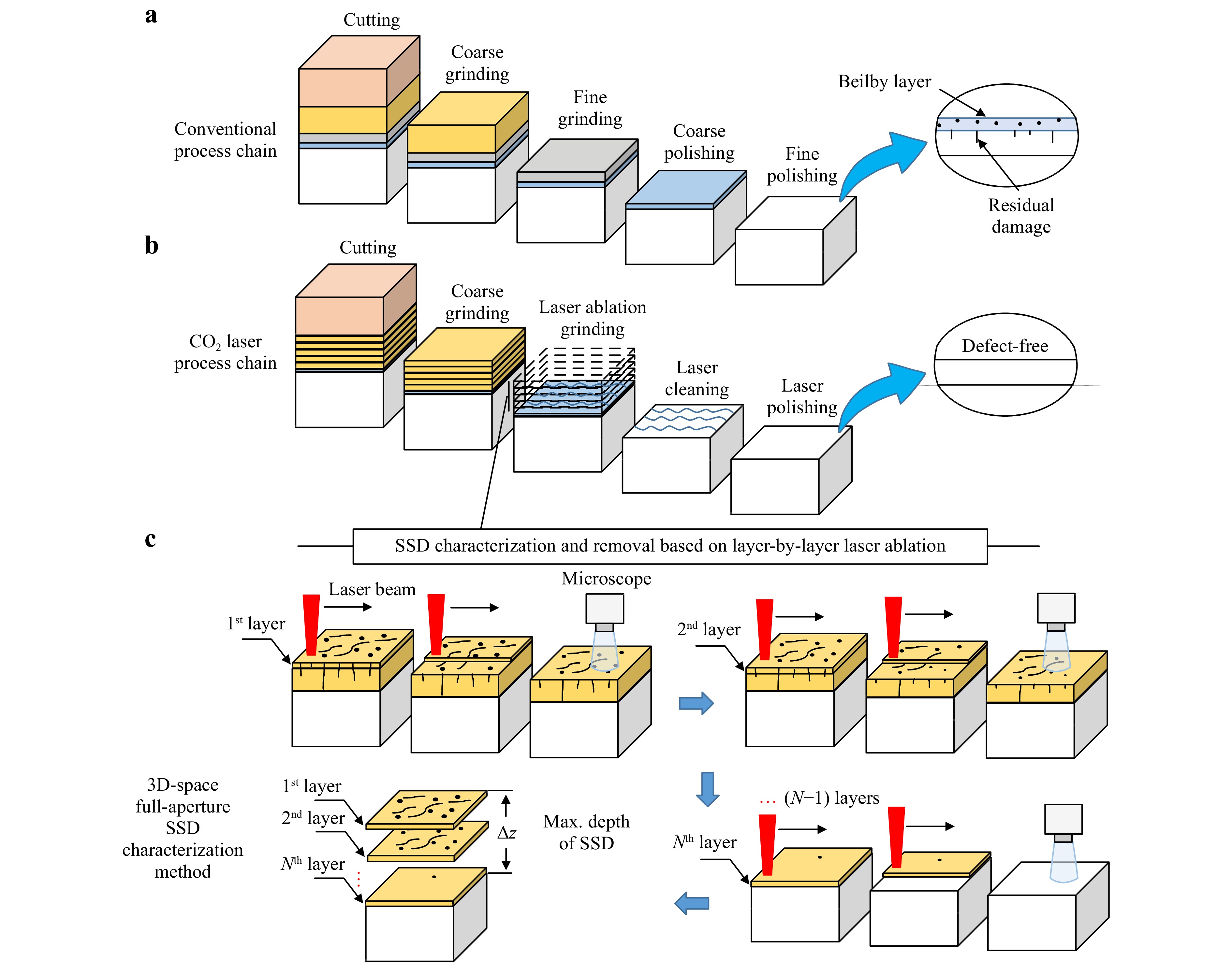
Fig. 1 Process chains for fused silica optics: a Conventional process chain; b CO2 laser process chain; c 3D-space full-aperture SSD characterization method.
-
To manufacture fused silica optics with a high LIDT, SSD generated during the grinding process must be effectively managed. An accurate spatial distribution and the maximum SSD depth for the grinding process must be obtained first. The SSD distribution is helpful in studying the SSD generation law and optimizing the grinding process; the maximum depth provides sufficient material depth for complete SSD removal. Given the limitations of current methods for characterizing SSD9, we propose a new 3D-space full-aperture SSD characterization method based on layer-by-layer laser ablation, as shown in Fig. 1c. For a sample containing SSD, we first removed a layer of material by laser ablation. The SSD was exposed to the surface and could be directly observed with a microscope. Layers were removed until no SSD was observed on the surface. At this point, according to the total number of layers removed (N layers) and the SSD information recorded for each layer, the maximum SSD depth (Δz) and 3D distribution of the SSD were obtained. The relationship between the removal depth and number of removed layers can be calibrated in advance using a profiler. With the aid of a 2D galvanometer and motion stage, the area of laser ablation is not limited; that is, we can characterize SSD in the sample in full aperture.
CO2 laser ablation is a thermal ablation process. Generation of thermal strain and stress during laser processing can lead to formation of microcracks. However, this can be avoided by optimizing the ablation parameters. Pulsed CO2 laser ablation has been successfully used to repair laser-induced surface damage sites on fused silica optics by removing the materials via evaporation2. We used pulsed CO2 laser ablation to remove materials and expose the microscale SSD generated during the grinding process, a main damage precursor at low fluences. To accurately characterize the maximum depth and spatial distribution of the SSD using pulsed CO2 layer-by-layer laser ablation, the following conditions must be met. First, laser ablation cannot produce new SSD, which prevents introduction of measurement errors. Second, laser ablation should be able to remove materials uniformly, layer-by-layer, to obtain the SSD distribution at different depths. The removal depth per layer was selected to satisfy different resolution requirements. We studied a theoretical uniform laser ablation process. Because the interaction between a CO2 laser and fused silica is a complex multiphysics coupling process, it is difficult to completely simulate the material ablation removal process. However, CO2 laser ablation is a thermal ablation process; changes that occur during the ablation process strongly depend on the temperature-field distribution. Thus, we can predict processing trends by simulating the temperature-field evolution. A transient temperature-field model was established to guide optimization of the ablation parameters. Conduction of the laser energy inside the material can be described by the following heat conduction equation:
$$ \rho {C}_{p}\left(T\right)\frac{\partial T}{\partial t}+\nabla \cdot \left(-K\left(T\right)\nabla T\right)=Q $$ (1) where ρ is the density; Cp(T) and K(T) are the specific heat capacity and thermal conductivity, respectively26; Q represents the laser heating source, expressed as
$$ Q=\alpha \frac{2(1-R)P}{\pi {\omega }_{0}^{2}}\mathrm{e}\mathrm{x}\mathrm{p}\left(-\frac{2{\left(x-{v}_{s}t\right)}^{2}}{{\omega }_{0}^{2}}-\alpha \left|y\right|\right)F\left(t\right) $$ (2) where α is the absorption coefficient, and R is the reflectivity. P is the peak power of the rectangular pulse; ω0 is the laser beam radius; vs is the scan speed along the x direction; F(t) is the time distribution function of the rectangular pulse. In Eq. 2, α and R is temperature-dependent and defined as
$$ \alpha =4\pi {n}_{k}\left(T\right)/\lambda $$ (3) $$ \mathrm{R}=\frac{{({n}_{i}-1)}^{2}+{{n}_{k}\left(T\right)}^{2}}{{({n}_{i}+1)}^{2}+{{n}_{k}\left(T\right)}^{2}} $$ (4) where ni and nk(T) (Ref. 27) are the real and imaginary components of the refractive index, respectively. λ denotes the wavelength of the CO2 laser. Fig. 2 shows a schematic of the two-dimensional model.
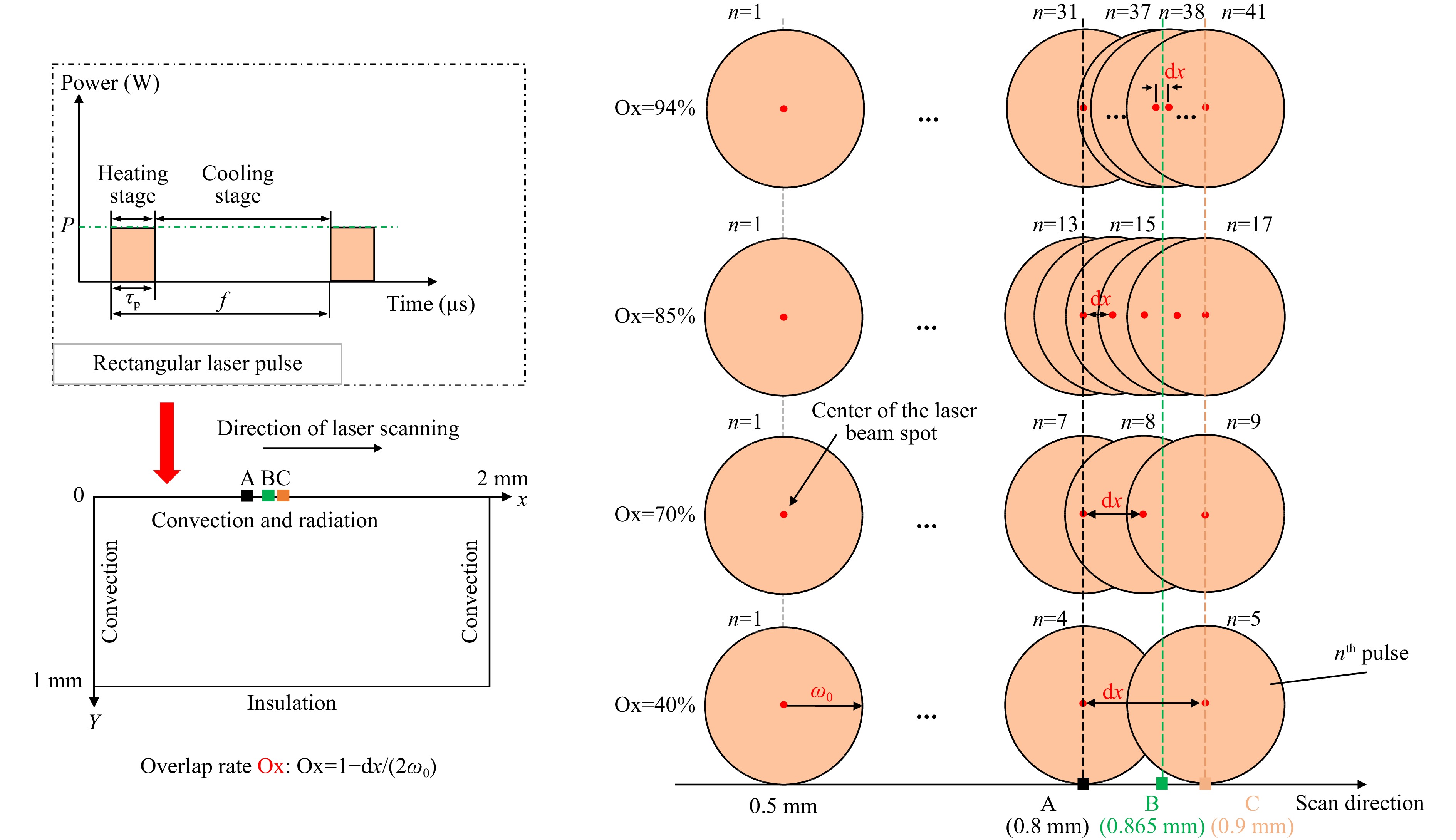
Fig. 2 Schematic of computation model.
Along the laser scanning direction, the ablation pulse distance dx=vs/f, where f is the pulse frequency. The overlap rate Ox (Ox=1-dx/(2ω0)) reflects the cumulative thermal effect between ablation pulses. Laser irradiation starts at a point (0.5 mm, 0). The global temperature and the temperature at point A (0.8 mm, 0), point B (0.865 mm, 0), and point C (0.9 mm, 0) are captured to analyze the influence of the irradiation parameters on the temperature field. We simulated the temperature field with different overlap rates by varying the scanning speed. Four scan speeds (100 mm/s (Ox=40%), 50 mm/s (Ox=70%), 25 mm/s (Ox=85%), and 10 mm/s (Ox=94%)) were used at f=1 kHz, as shown in Fig. 2. With this setting, for different overlap rates, when the center position of the laser beam spot moved to points A and C, points A and C were always in the heating stage of the rectangular pulse. When it moved to point B, point B was always in the cooling stage of the rectangular pulse. The other parameters used in the simulation are presented in Table 1.
Table 1. Simulation parameters
Fig. 3 shows the surface temperature distribution at different times along the laser scanning direction with different overlap rates. After a period of laser irradiation, the maximum temperature of the surface with different overlap rates quickly reached a stable value (Fig. 3a−c). This indicates that CO2 laser ablation can achieve stable removal of the material. However, if the overlap rate is too high, the maximum surface temperature cannot be stabilized quickly (Fig. 3d) and stable removal cannot be achieved.
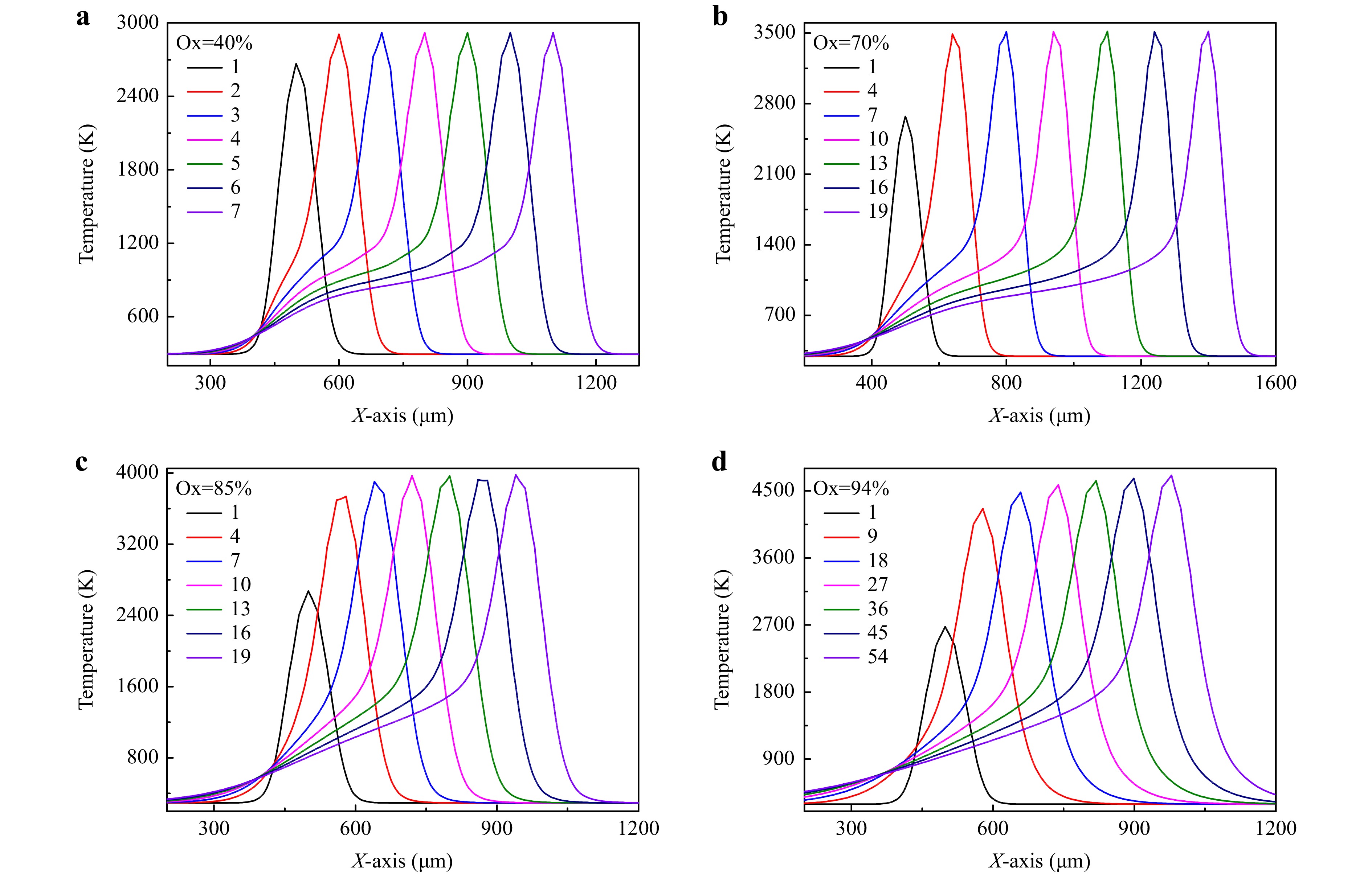
Fig. 3 Simulation results for surface temperature distribution after laser irradiation with different overlap rates Ox: a Ox=40%; b Ox=70%; c Ox=85%; d Ox=94%. The pulse width τp = 40 us. The number of the legend represents the number of pulse, for example, 1 represents the surface temperature distribution when the laser just stopped heating during the first pulse irradiation, 2 represents the surface temperature distribution when the laser just stopped heating during the second pulse irradiation, and so on.
By monitoring and analyzing the temperature changes at different locations along the laser irradiation path, we can compare the temperature rise and fall processes at different locations, as shown in Fig. 4. Although the stable ablation state can be quickly achieved with Ox=40%, 70%, and 85%, this does not mean that uniform material removal can be achieved along the ablation path with these overlap rates. As shown in Fig. 4a, at a low overlap rate of Ox=40%, with heating by heat conduction and laser beam edge, point B was still insufficient to reach the maximum temperature above the vaporization temperature (Tv = 2500 K). This resulted in separate single-pulse ablation morphologies along the laser scanning direction. With an increase in the overlap rate, point B can also exceed the vaporization temperature (Fig. 4b), with a gradual rise and fall process similar to that at points A and C (Fig. 4c) to achieve uniform removal. Thus, an appropriate overlap rate is the key to achieving uniform material removal. In subsequent experiments, an overlap rate of Ox= 85% was used to achieve uniform material removal.
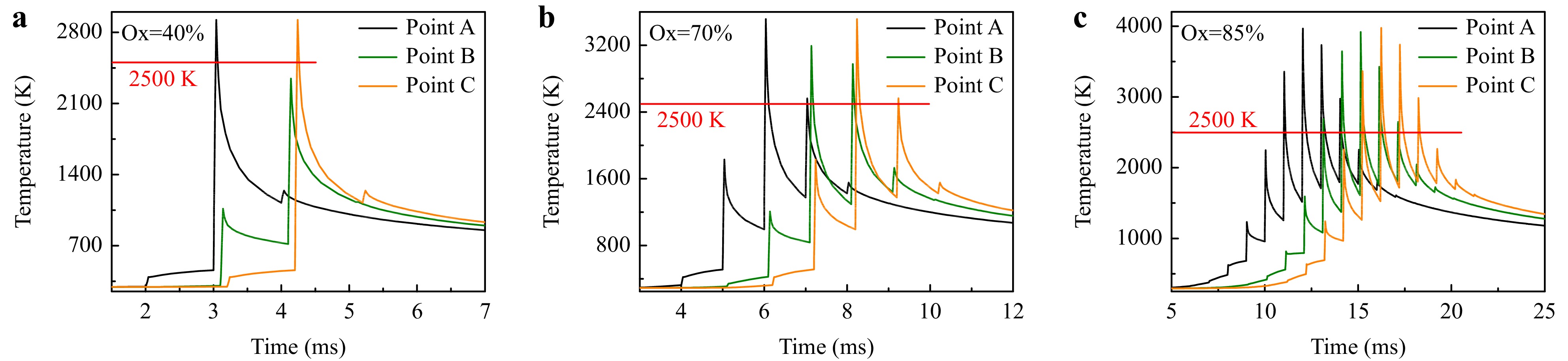
Fig. 4 Simulation results for temperature evolution over time at points A, B, and C with different overlap rates Ox: a Ox=40%; b Ox=70%; c Ox=85%. The pulse width τp = 40 us, and vaporization temperature Tv = 2500 K. To clearly display the results, the temperature evolution over time at point B and point C is artificially delayed by 0.1 ms and 0.2 ms, respectively.
Further analysis shows that although uniform removal of materials can be achieved with Ox=85%, the temperature at the same location exceeds the vaporization temperature for many times (Fig. 4c) and over-ablation occurs, decreasing the roughness of the surface. As shown in Fig. 5a, over-ablation can be suppressed by changing the ablation pulse width τp. When the ablation pulse width was reduced, only one ablation occurred at the same position. This implies that laser ablation does not worsen the original surface roughness and uniformly removes material. This is important for high-precision material-removal processes.
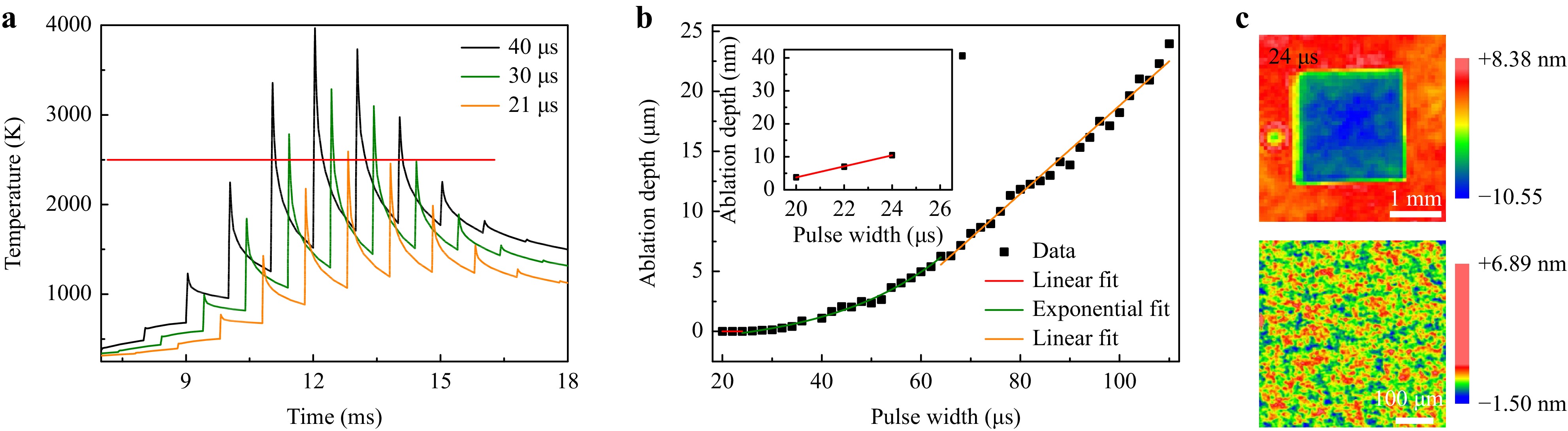
Fig. 5 a Temperature evolution over time at point A with different pulse widths; b Experimental results for ablation depth as a function of pulse width; the inset graph is an enlarged view of the linear fitting region; c White-light interferometer images of ablated field with τp = 24 us, depth of ablation area ~ 10.5 nm, RMS = 0.386 nm.
To verify the evolution trend of the ablation characteristics with the pulse width, as demonstrated in the simulation, we conducted local laser ablation experiments with different pulse widths on a series of flat, conventionally polished fused silica samples. The experimental setup is described in the Materials and Methods section. During the experiments, an ablation field of 2 mm × 2 mm was applied for each set of pulse widths and a unidirectional raster scanning strategy was used. The laser beam focused on the front surface of the samples was unchanged, with a laser peak power of P=26.5 W and an overlap rate of Ox=85% (scan speed vs=25 mm/s, pulse frequency f=1 kHz) fixed. All ablation fields were measured using a white-light interferometer to obtain the ablation morphology and depth. Fig. 5b shows the relationship between ablation depth and ablation pulse width. A uniform ablation depth from nm to um can be achieved by changing the ablation pulse width. When the pulse width was reduced to 24 us, material removal was achieved in the ablation area and the initial sub-nanometer surface roughness was maintained, as shown in Fig. 5c. Perfect ablation results were obtained with an ablation depth less than 10 nm; a minimum ablation depth of < 5 nm was realized, as shown in the inset graph in Fig. 5b.
-
The theory reveals a method for uniformly removing materials by laser ablation and predicts the conditions for high-precision ablation. As such, the relationship between the ablation depth and pulse width was experimentally established. In this section, we also demonstrate through experiments that laser ablation does not introduce SSD, resulting in accurate characterization of the SSD distribution. Based on layer-by-layer laser ablation, an SSD-free surface can be obtained, and chemical structural defects on the surface are suppressed.
Fig. 6 shows an example of using the new method to characterize the SSD distribution. During characterization, SSD is exposed to the observation surface by removing material layer-by-layer. Notably, some ablation products were redeposited on the surface during laser ablation, particularly with a large amount of material removal. The redeposited ablation products covering the surface may affect the SSD observations using a microscope. To avoid deposition of ablation products as much as possible, the suction device was kept open at all times to collect ablation products during the experiments. Even with a single-layer removal depth up to 20 um, there were not significant ablation products redeposited on the surface after ablation, as shown in microscopic images 1–5 in Fig. 6 (the specific layer-by-layer ablation process is shown in Fig. 7a). The microcracks and ablation products are significantly different and are easily distinguished in the microscopic images. Thus, this method can provide direct observation of SSD, and subsequent chemical etching and cleaning steps are not required, unlike with other destructive characterization methods9.
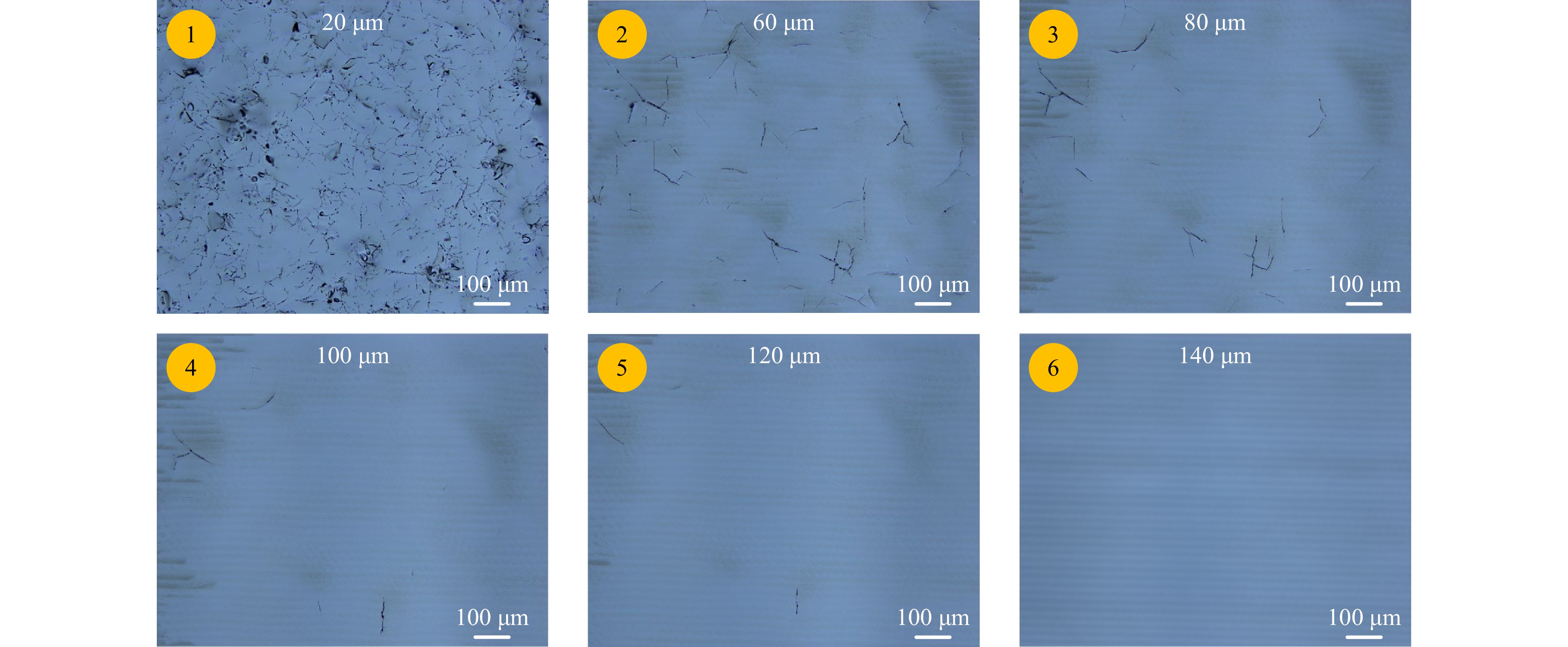
Fig. 6 Defect distribution as a function of depth at the same sample location (ground with W100) after layer-by-layer laser ablation. All images in the figure have a scale of 100 um.
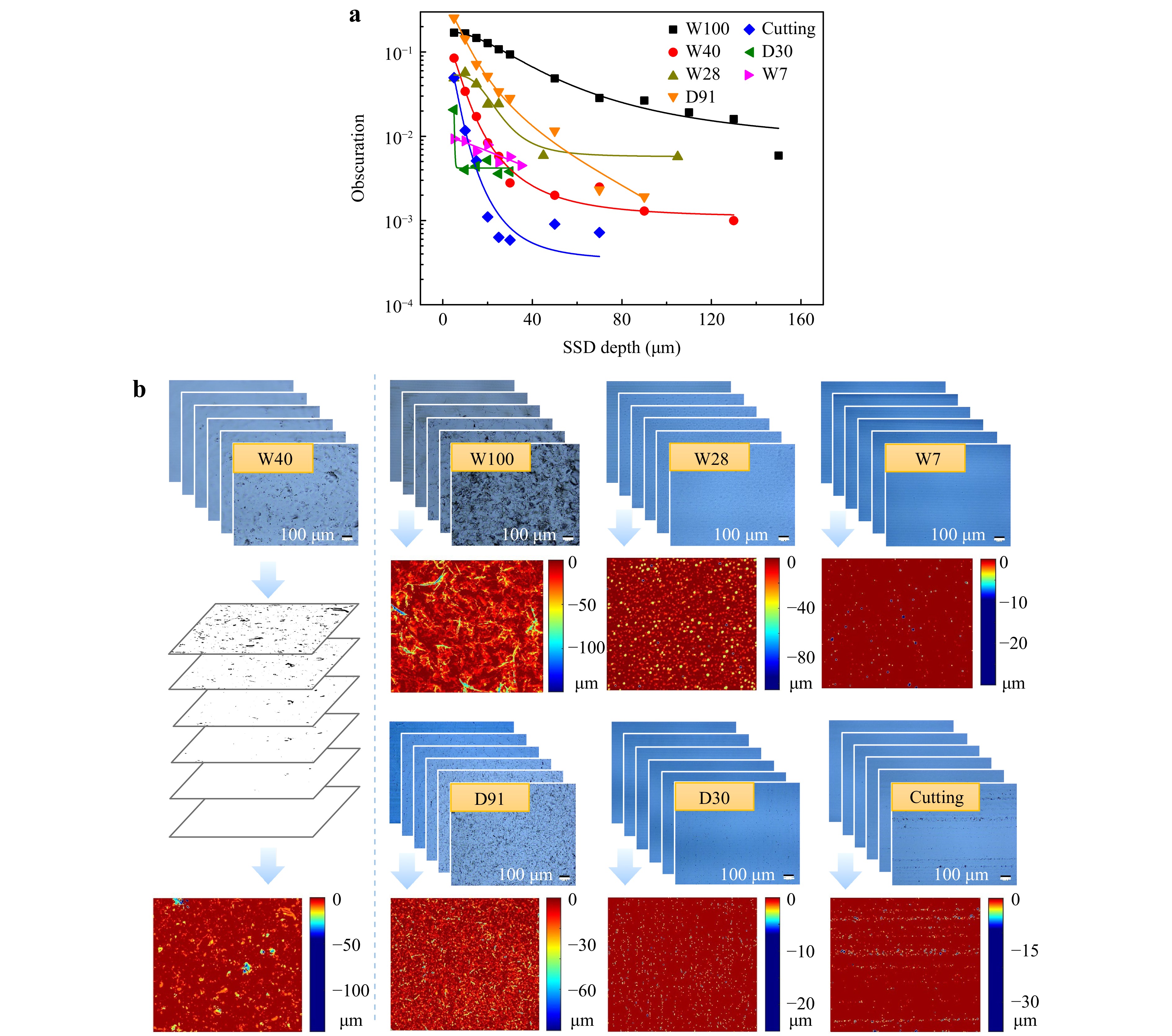
Fig. 7 SSD distribution as a function of depth into the surface: a Distribution of SSD depths observed at the same location with laser ablation and image analysis of different samples; b 3D-space morphology of SSD in samples with different process conditions.
Further analysis of the microscopic images of the SSD at different depths in Fig. 6 indicated many lateral cracks in the subsurface layer 20 μm from the surface. Moreover, many breaking areas, Hertzian corn cracks caused by blunt pressure, were apparent. With a further increase in depth, the crack density decreased significantly, and the sizes of the individual cracks gradually decreased until they disappeared, indicating that laser ablation did not cause the cracks to continue to extend downward. In comparing the crack distributions at different depths, we found no new cracks in the deeper subsurface layer, only the original cracks, indicating that there was no new SSD during the laser ablation process. This implies that laser ablation can be used as an SSD-free grinding tool for removing materials.
Similarly, layer-by-layer laser ablation was performed on samples ground with different abrasives. To better compare the characteristics of SSD with different processes, the defect area fraction relative to the observed area (obscuration), was used to estimate the variation tendency of the SSD, as shown in Fig. 7a. To obtain a larger observation area to improve the statistical accuracy and clearly observe the defects, SSD exposed on the surface was recorded at a magnification of 10x (NA=0.3). This resolution is sufficient to characterize and evaluate microscale cracks generated during the grinding process (as shown in Fig. 6), a primary damage precursor at low fluences. With uncertainties and their limitations, current SSD prediction methods cannot accurately guide SSD depth in different processing conditions. However, with laser ablation and rapid image processing, we can characterize the SSD distribution from the surface to a depth of several hundred microns and deeper. Using image algorithms, the recorded images of each layer are binarized, then fused in 3D-space to obtain the 3D-space SSD morphology. Fig. 7b shows the 3D-space SSD morphology in samples with different process conditions. For loose corundum abrasives, W100 and W40 were distributed with a large number of Hertzian corn cracks caused by blunt pressure due to large particle size, appearing as brittle fracture areas with a diameter of approximately 50–100 μm. In contrast, there were many radial cracks in the shape of the broken points in the W28 sample. The number of defect points in the W7 sample was significantly less than that in W28, which further indicates that smaller particle sizes cause less brittle fracture and radial defect extension. However, loose abrasives easily agglomerate or introduce large-particle impurities, resulting in individual radial defects extending to a deeper layer, up to hundreds of microns. In the wire-cut sample, the defects were mainly distributed at the positions of the linear cutting traces. With layer-by-layer laser ablation, the cutting traces and defects gradually disappeared. For fixed abrasives, a large number of lateral cracks are expected to result in more rapid material removal. After removing 40 μm for the D30 sample, there were almost no obvious defects. Thus, in subsequent SSD removal experiments, we selected samples ground with D30 to improve the processing efficiency.
With fabrication processes and impurities in raw materials, breakage of Si-O covalent bonds, loss of oxygen ions, and oxygen/silicon interstitials destroy the integrity of the tetrahedral structure of fused silica and introduce chemical structural defects such as nonbridging oxygen hole centers and oxygen-deficient centers29. A fluorescence spectrometer was used to measure and analyze the evolution of the chemical structural defects on the surface of the sample before and after laser ablation. As shown in Fig. 8a, compared with the original ground surface, the photoluminescence (PL) signal of the ground surface after laser ablation was significantly reduced in intensity. As laser ablation removed the material layer-by-layer, the intensities of the PL band increased only slightly, as shown in Fig. 8b. This implies that laser ablation can also mitigate chemical structural defects, and that the residual heat-affected area is limited and does not accumulate with an increase in the number of ablation layers. The intensity of the PL band at ~550 nm increased after laser ablation compared to the PL band at ~420 nm (attributed to the $ {\text{O}}_{\text{2}}^{\text{-}} $)13. The PL band at ~550 nm has not yet been clearly interpreted but may be related to the structural disorder of fused silica30 caused by the high-temperature removal process of pulse laser ablation. The high temperature caused the mesh structure of the fused silica to change through structural relaxation.
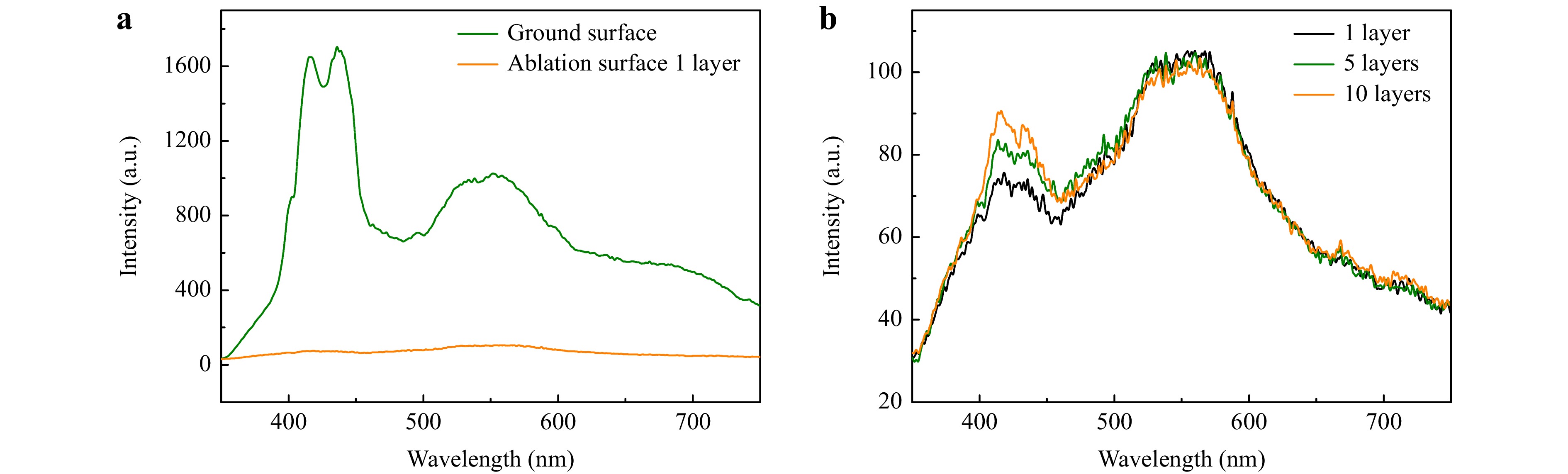
Fig. 8 PL spectra for D30 ground surface and ablation surface: a PL spectra for ground surface before and after laser ablation one layer; b PL spectra for ablated surfaces after laser ablation different layers. The excitation wavelength was 325 nm; the ablation depth of a single layer was ~20 μm.
-
The theoretical and experimental results indicate that compared to traditional SSD characterization methods such as MRF taper polishing, our proposed characterization method can directly expose the SSD to the observed surface without the need for a subsequent HF etching step. Because the area and depth of laser ablation are not limited, and new SSD is not introduced, the maximum depth and spatial distribution information of the entire component can be accurately obtained. Although this method is destructive, it can be used as an SSD-free grinding tool. That is, it can simultaneously characterize and remove SSD. Thus, we can couple this method as a laser grinding step with a material removal process (Fig. 1) to obtain an SSD-free surface. Chemical structural defects on the surface were suppressed. Our previous study24 showed that laser melt polishing can achieve a super-smooth surface and suppress defects. Based on these conclusions, a CO2 laser process chain was proposed to manufacture fused silica optics with a high LIDT, in which the grinding steps were replaced by layer-by-layer laser ablation, and the polishing steps were replaced by laser melt polishing.
For verification, samples were prepared using conventional and CO2 laser process chains. In the CO2 laser processing chain, the D30 ground sample was ablated layer-by-layer to remove the SSD until a surface with no scratches or cracks was observed. Although an ablation product collection device was used in the experiment, some products were redeposited on the surface with a large amount of material removed; these were difficult to remove via ultrasonic cleaning with deionized water. Thus, an additional laser conformal cleaning step was used to remove the surface-redeposited ablation products before laser melt polishing. According to the relationship between the ablation depth and pulse width shown in Fig. 5b, laser conformal cleaning experiments with different cleaning depths were conducted to optimize the cleaning depth. During the laser conformal cleaning experiments, each cleaning depth was achieved by laser ablation of one layer rather than layer-by-layer ablation. The microscopic images in Fig. 9a show the surfaces after laser cleaning at different cleaning depths. It was observed that cleaning became more effective as the cleaning depth increased. When the cleaning depth reached 100 nm, the redeposits were removed. However, when the cleaning depth was too deep, the ablation products produced during the laser cleaning process were deposited on the surface. Laser ablation is accompanied by a slight material melting process, and some contamination may be embedded in the subsurface layer. Thus, XPS was used to analyze the longitudinal distribution of contaminants. C was selected as a representative. As shown in Fig. 9b, after layer-by-layer laser ablation, the contamination depth of C was greater than 45 nm, and laser cleaning could effectively remove the contamination. With increasing cleaning depth, the depth of the contamination layer was less than 15 nm; however, a cleaning depth that was too deep introduced a new contamination layer. An appropriate cleaning depth can effectively remove surface and subsurface contaminants simultaneously. A cleaning depth of 100 nm was chosen for the laser conformal cleaning step to clean the ablated surface and remove ablation contaminants without introducing new contaminants. Fig. 10 shows the evolution of the sample surface morphology in the CO2 laser processing chain.
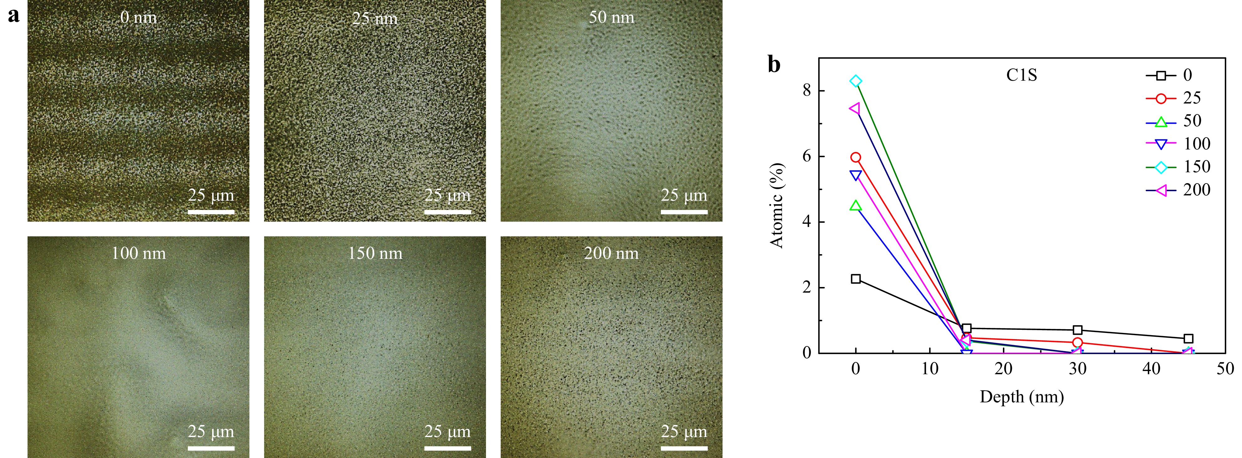
Fig. 9 Contamination removal effect with different cleaning depths: a Microscopic images of ablated surface after laser cleaning with different cleaning depths; b XPS measurement results for C content at different depths in longitudinal direction of ablated samples after treatment with different laser cleaning depths.
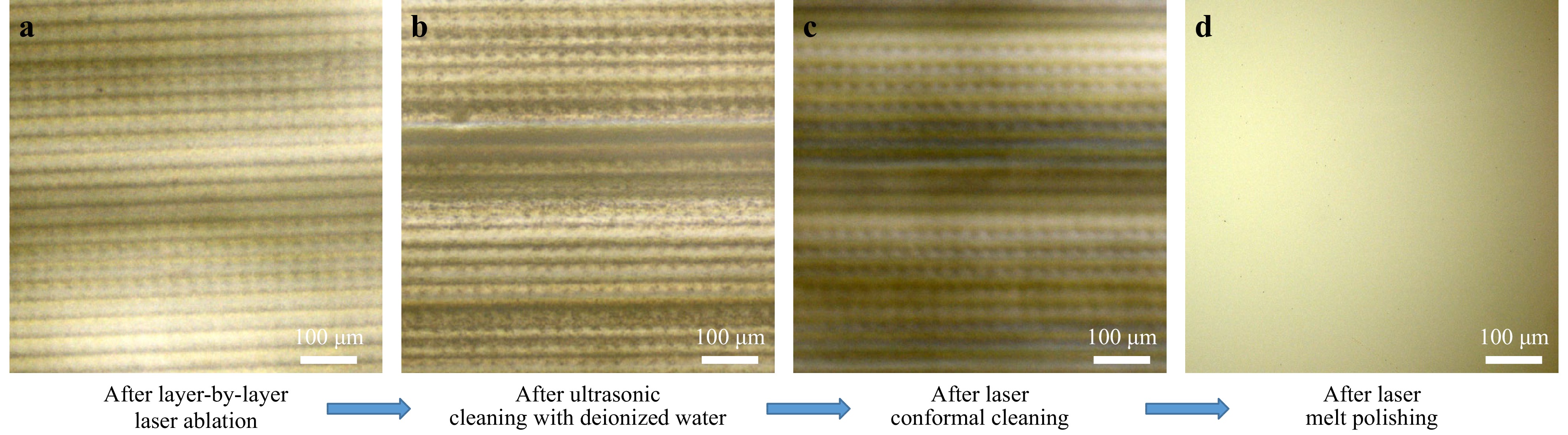
Fig. 10 Evolution of sample surface morphology in CO2 laser processing chain: a Microscopic image of surface after layer-by-layer laser ablation; b Microscopic image of surface after ultrasonic cleaning with deionized water; c Microscopic image of surface after laser conformal cleaning; d Microscopic image of surface after laser melt polishing.
After the samples were prepared, their anti-UV laser damage performance was investigated. The damage test results indicated that the CO2 laser process chain can be used to manufacture fused silica optics with a high LIDT. As shown in Fig. 11a, the damage resistance of the sample fabricated using the CO2 laser process chain was significantly improved. Compared with the 0% probability LIDT (20.5 J/cm2) and the 100% probability LIDT (30 J/cm2) of the sample made using the conventional process chain, the 0% probability LIDT (28.9 J/cm2) of the sample made using the CO2 laser process chain was increased by 41%, and the 100% probability LIDT (49.7 J/cm2) was increased by 65.7%. The increase in the LIDT was also reflected in the degree of inhibition of chemical structure defects (Fig. 11b) and damage morphology (Fig. 11d−g). For the samples prepared using the conventional process chain, many small damage points were distributed in the laser irradiation area. With an increase in the irradiation fluence, these small damage points were connected to form a very large damage site; for the sample prepared using the CO2 laser process chain, there were no small damage points around the main damage site, and with an increase in the irradiation fluence, the damage size did not increase significantly. This indicates that with the tested fluence, the damage precursors were not the same in the two process chains. The CO2 laser process chain (Method A) effectively inhibited the damage precursor with the high density and low damage threshold present in the conventional process chain. In our previous study24, we attempted to directly heal the SSD using laser melt polishing, but the healing depth was limited. The residual SSD resulted in limited LIDT improvement. To address the issue of insufficient healing depth in laser melt polishing, we further proposed using HF etching to fully expose and open the SSD before laser melt polishing (Method B), achieving a significant increase in LIDT. The role of HF etching was similar to that of the laser ablation grinding process in this study. Although the final LIDT enhancement effect was similar, Method A, which included the laser ablation grinding process, clearly shows greater potential for defect suppression and LIDT improvement. As shown in Fig. 11 in this study and Fig. 4 in Ref. 24, with similar laser fluences, the damage density of Method A was much lower than that of Method B. This is because the HF etching step in Method B generated many etching products ($ \text{Si}{\text{F}}_{\text{6}}^{\text{2-}} $)4, which combined with cations (such as K+, Na+) in deionized water to form nanoscale salt deposits. These salt deposits were difficult to clean and remove. Without a material removal process in the subsequent laser melt polishing step, residual salt deposits were embedded on the surface/subsurface of the sample. These salt deposits, along with the contaminants introduced during the cleaning and drying steps before damage testing, became high-fluence damage precursors. However, Method A did not have the problem of salt deposits; thus, the damage density of Method A was significantly less than that of Method B. Due to difficulty in controlling the HF etching process and removing salt deposits before laser melt polishing, LIDT improvement using Method B was more unstable. However, in Method A, the laser ablation grinding process was stable and controllable, and the ablation products were removed by the laser cleaning process before laser melt polishing.
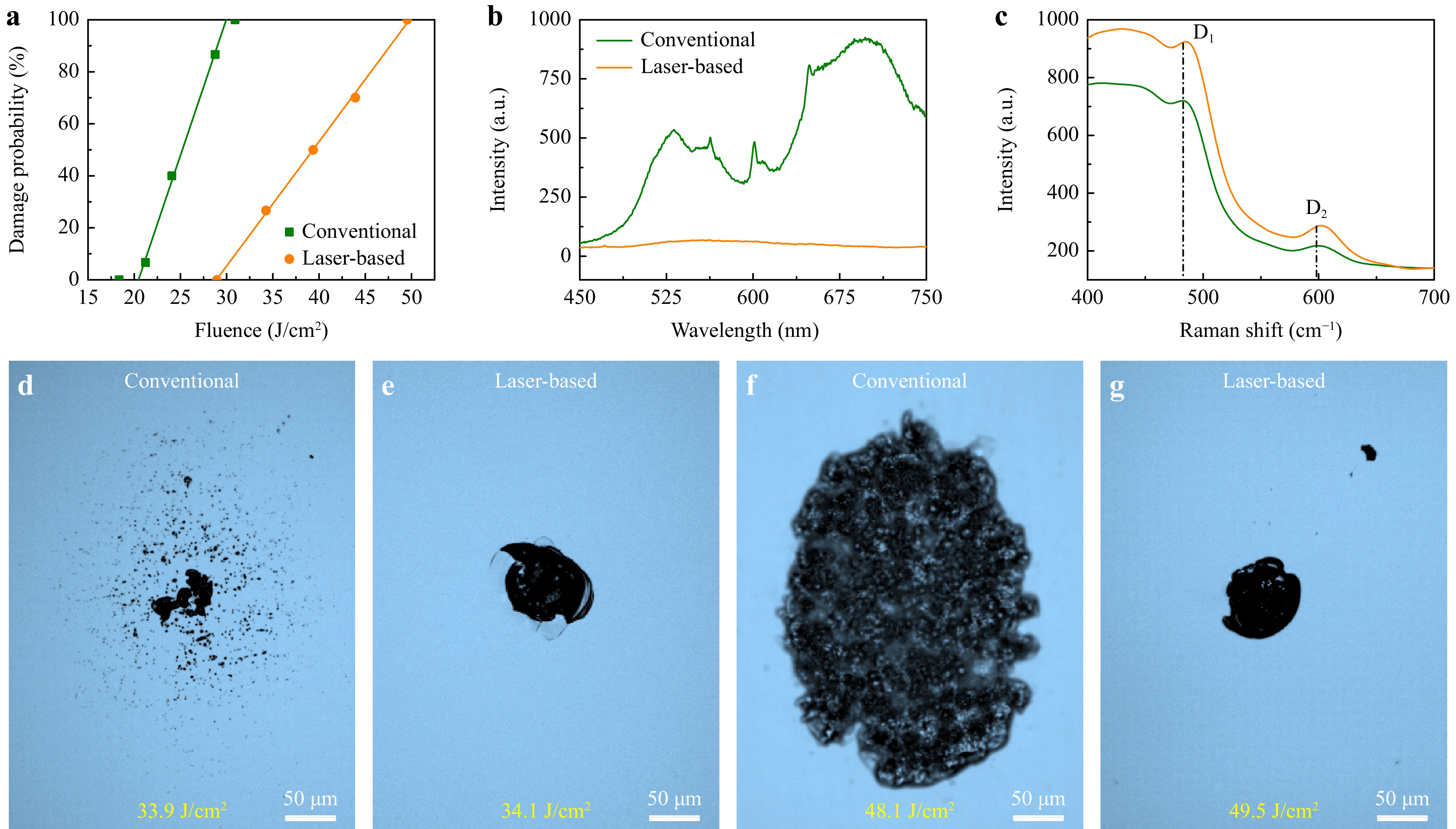
Fig. 11 Characterization results for prepared samples: a 1-on-1 damage probability as a function of fluence; b PL spectra of samples made by different chains; the excitation wavelength was 405 nm; c Raman spectra of samples with different chains; the excitation wavelength was 633 nm; d–g. Microscopic images of typical laser-damage morphologies of samples prepared using different process chains with similar laser fluence.
Because the CO2 laser process chain is a noncontact process, a higher LIDT should theoretically be obtained. A possible reason for the limited increase in the LIDT is the presence of nanoscale precipitates on the sample surface during cleaning and drying. In addition, the thermal effect of CO2 laser processing may limit LIDT improvement. Although the laser-based process chain can suppress chemical structural defects more effectively than the conventional process chain, the structural disorder caused by thermal strain may generate ~550-nm PL defects (Fig. 8b), which may be related to the laser-induced damage of the fused silica optic30. The thermal effect causes the D1 and D2 peaks (resulting from the symmetric breathing modes of the 4- and 3-membered rings, respectively) to shift to higher wavenumbers (Fig. 11c), resulting in greater densification of the processed surface31. The strained Si-O-Si bonds in the 3- and 4-membered rings with high-fluence laser irradiation may be broken to form chemical structural defects32.
-
A laser-based defect characterization and removal process for manufacturing fused silica optics with a high ultraviolet laser damage threshold was investigated. A 3D-space full-aperture characterization method based on layer-by-layer laser ablation was proposed to characterize SSD. The feasibility of uniform laser ablation was theoretically analyzed by establishing a temperature-field model. Under the guidance of the model, the relationship between the uniform laser ablation depth and pulse width was established experimentally; a minimum ablation depth of < 5 nm was realized. Experiments on cutting and grinding samples showed that laser ablation does not introduce SSD, demonstrating that uniform layer-by-layer laser ablation can characterize the SSD distribution in a 3D-space with full aperture, and act as an SSD-free grinding tool to remove SSD completely. Moreover, uniform laser ablation at a 100-nm depth can also be used as a conformal cleaning tool to effectively remove surface/subsurface ablation contamination. Based on these conclusions, a noncontact process chain including laser ablation, laser cleaning, and laser melt polishing was further developed to manufacture fused silica optics with a high LIDT. Owing to the advantages of the CO2 laser process chain in controlling defects, the LIDT of the sample fabricated using the CO2 laser process chain was 41% (0% probability) and 65.7% (100% probability) higher than that of samples prepared using the conventional process chain. This new laser-based defect characterization and removal strategy indicates a new direction for manufacturing fused silica optics with a high LIDT. The proposed SSD characterization method can also be used in a conventional process chain to guide optimization of the finishing process. Current quantitative characterization methods evaluate SSD depth indirectly by measuring a test piece, which highlights the potential of laser-based defect characterization and removal methods, especially in processing large-aperture components. Introduction of a machine vision system will enable online SSD characterization and removal for large-aperture optics. The layer-by-layer laser cleaning is a potential replacement technique for iron beam figuring of surfaces with an initial submicrometer surface roughness. Our proposed method can also be extended to other material processing with defect control requirements. Further research on the negative thermal effects of CO2 laser processing chains will be conducted in the future.
-
The laser ablation and cleaning experiments were performed using a laser ablation setup (Fig. 12). A CO2 laser (Coherent Cx-10L 10.6) with a maximum output power of approximately 120 W was used in the LA setup. In our experiments, a laser was used at a high modulation rate (95 kHz) to generate a quasi-CW output. The laser output was modulated into rectangular pulses with a frequency of 1 kHz using an acousto-optic modulator. The rectangular pulsed laser was expanded and guided over the sample using a 2-D galvanometer scanner. An F-theta lens with a focal length of f = 100 mm was used to focus the laser beam, resulting in a focal diameter of d=167 μm (1/e2). The peak power of the laser irradiating the sample was 26.5 W. The sample was positioned on an XYZ 3-D motion stage. The Y-axis of the motion stage was used to adjust the laser focus on the sample surface; the XZ-axes were used to select the ablation area. A unidirectional raster-scanning strategy was used in the laser ablation and cleaning experiments.
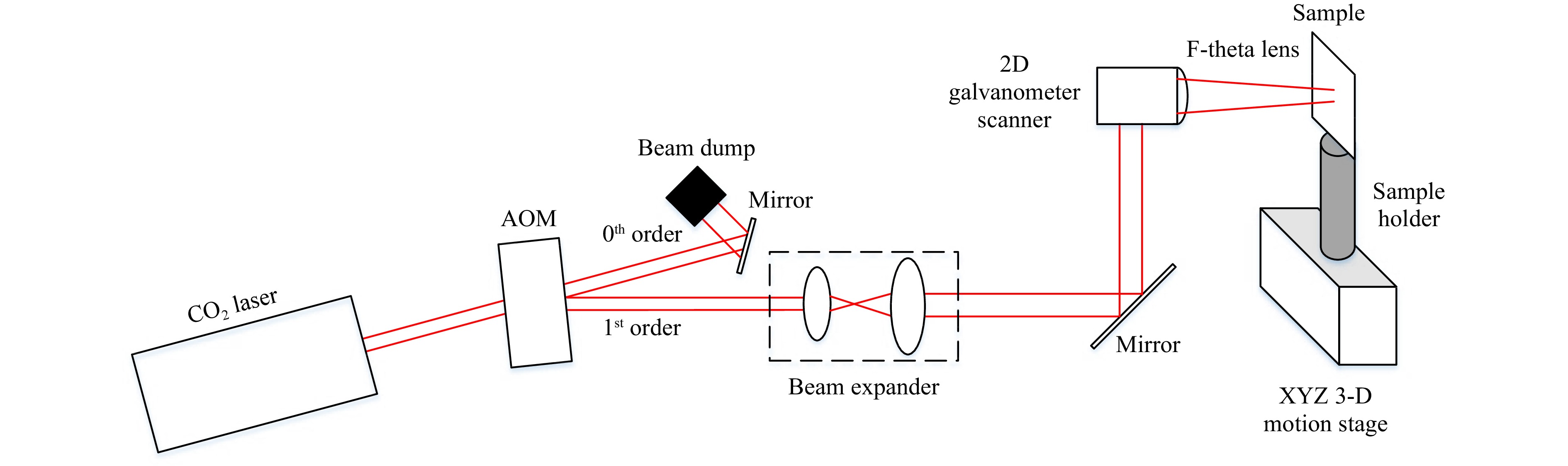
Fig. 12 Diagram of experimental laser ablation setup.
A suction device (KN103, Shenzhen City Weinan Technology Co., Ltd.) was used to collect the ablation products. This device provides a maximum airflow of 300 mm3/h and a maximum filtering efficiency of 0.3 um 99.99%. The ablation products were sucked into the multifiltration system through the single-arm channel (diameter = 75 mm) of the device and then adsorbed and intercepted. During the laser ablation experiments, the device was kept open at the maximum flow at all times to collect the ablation products.
-
The fused silica samples (Heraeus Suprasil 311) were wire-cut to 30 mm × 30 mm × 12 mm from the same fused silica boule. In SSD characterization, a series of pre-polished silica samples were manufactured using the conventional polishing process with a 1-μm CeO2 slurry. Six samples (W100, W40, W28, D91, D30, and W7) were ground with loose corundum abrasive (100 μm, 40 μm, and 28 μm), fixed corundum abrasive (91 μm and 30 μm), and 7-μm loose B4C abrasive. In terms of SSD removal, two cutting samples were simultaneously ground by 30-μm fixed corundum abrasive to remove 600 μm for subsequent manufacture of damage test samples. The sample made using the conventional process chain was polished with a 1-μm CeO2 slurry (prepared by Shanghai Hengyi Optics and Fine Mechanics Co., Ltd). The sample was submerged in a megasonic-agitated HF-based etchant bath for 30 min to remove the Beilby layer. The HF-based etchant consisted of deionized water, 47 wt.% HF, and 23 wt.% NH4F in a volume ratio of 14:1:25. The etching rate was maintained at 30 nm/min. The sample was prepared using the CO2 laser process chain: 1) the ground sample was ablated layer-by-layer (Ox=85%, τp=102 μs, ~20 μm per layer) using the laser ablation setup; the total ablation depth was ~100 μm. 2) The sample was cleaned with deionized water. 3) Laser cleaning was performed using the laser ablation setup. In the cleaning experiment, the pulse width τp of the rectangular pulse was set to 28 μs (~100 nm depth). 4) The sample was cleaned with deionized water. 5) A self-built laser melt polishing setup24 was used to polish the sample at a scan speed of 16 mm/s and a scan pitch of 50 μm. Before the damage test, all samples were cleaned with deionized water. The samples were submerged in an ultrasonically agitated deionized water bath for 5 min, sprayed with deionized water for 5 min, and carefully air dried.
Images were obtained using an Olympus microscope (OLYMPUS BX53). The images in Fig. 6, Fig. 7, Fig. 10, and Fig. 11 were recorded at a magnification of 10x (NA=0.3); the images in Fig. 9 were recorded at a magnification of 50x (NA=0.8). The ablation depths in Fig. 5b were obtained by comparing the height differences inside and outside the ablation fields. All ablation fields were measured using a white-light interferometer (Zygo Newview 7300) at a magnification of 10x. As shown in Fig. 5c, the surface profile was measured using a white-light interferometer at a magnification of 1x; the surface roughness was measured at a magnification of 20x. The ablation depths shown in Figs. 6 and 7 were measured using a stylus profilometer (Form Talysurf PGI 1250). The PL and Raman spectra were measured using a PL spectrometer (Horiba iHR550) and a Raman spectrometer (Renishaw inVia), respectively. The elemental content was measured using an x-ray photoelectron spectrometer (XPS, Thermo Scientific).
Damage studies of the fused silica samples were conducted at a damage test facility. Damage testing was performed using a tripled Nd:YAG laser operated at 355 nm with a pulse width of 8.3 ns and a repetition rate of 10 Hz. The 1-on-1 LIDT was determined according to ISO 21254. The effective beam size on the sample surface was ~0.29 mm2; ten sites were tested for each energy fluence.
-
This work was supported by the National Key Research and Development Project (2022YFB3403400), Shanghai Sailing Program (20YF1454800), National Natural Science Youth Foundation of China (62205352), Natural Science Foundation of Shanghai (21ZR1472000), Key Projects of the Joint Fund for Astronomy of the National Natural Science Funding of China (U1831211), and the Youth Innovation Promotion Association of the Chinese Academy of Sciences.
Laser-based defect characterization and removal process for manufacturing fused silica optic with high ultraviolet laser damage threshold
-
Xiaocong Peng1, 2, 3,
 ,
, - Xin Cheng1, 2, 3,
-
Chaoyang Wei1, 2, 3, *, ,
,
- Songlin Wan1, 2, 3,
- Kaizao Ni1, 2, 3,
- Zhenqi Niu1, 2, 3,
- Yichi Han1, 2, 3,
- Zhigang Jiang1, 2, 3,
- Zhen Cao1, 2, 3,
-
Jianda Shao2, 3, 4, *, ,
- Light: Advanced Manufacturing 4, Article number: (2023)
- Received: 22 May 2023
- Revised: 27 June 2023
- Accepted: 10 July 2023 Published online: 20 July 2023
doi: https://doi.org/10.37188/lam.2023.021
Abstract: Residual processing defects during the contact processing processes greatly reduce the anti-ultraviolet (UV) laser damage performance of fused silica optics, which significantly limited development of high-energy laser systems. In this study, we demonstrate the manufacturing of fused silica optics with a high damage threshold using a CO2 laser process chain. Based on theoretical and experimental studies, the proposed uniform layer-by-layer laser ablation technique can be used to characterize the subsurface mechanical damage in three-dimensional full aperture. Longitudinal ablation resolutions ranging from nanometers to micrometers can be realized; the minimum longitudinal resolution is < 5 nm. This technique can also be used as a crack-free grinding tool to completely remove subsurface mechanical damage, and as a cleaning tool to effectively clean surface/subsurface contamination. Through effective control of defects in the entire chain, the laser-induced damage thresholds of samples fabricated by the CO2 laser process chain were 41% (0% probability) and 65.7% (100% probability) higher than those of samples fabricated using the conventional process chain. This laser-based defect characterization and removal process provides a new tool to guide optimization of the conventional finishing process and represents a new direction for fabrication of highly damage-resistant fused silica optics for high-energy laser applications.
Research Summary
Laser-based process chain: approaching defect-free manufacturing
A non-contact energy field processing method based on laser shows promise for manufacturing of optical components with high damage resistance to laser. Fused silica optics, a kind of optics which is widely used in high-energy laser system, its performance and life have been limited by the laser-induced damage caused by processing defects. Chao-Yang Wei from Shanghai Institute of Optics and Fine Mechanics and colleagues now report the use of CO2 laser to detect and remove defects during the processing of fused silica optics. The team demonstrated CO2 laser ablation can realize a 3D-pace full-aperture characterization of subsurface mechanical damage and obtain a microcrack-free surface. By adopting a CO2 laser process chain including laser ablation, laser cleaning and laser polishing, a fused silica component with high damage threshold was fabricated.
Rights and permissions
Open Access This article is licensed under a Creative Commons Attribution 4.0 International License, which permits use, sharing, adaptation, distribution and reproduction in any medium or format, as long as you give appropriate credit to the original author(s) and the source, provide a link to the Creative Commons license, and indicate if changes were made. The images or other third party material in this article are included in the article′s Creative Commons license, unless indicated otherwise in a credit line to the material. If material is not included in the article′s Creative Commons license and your intended use is not permitted by statutory regulation or exceeds the permitted use, you will need to obtain permission directly from the copyright holder. To view a copy of this license, visit http://creativecommons.org/licenses/by/4.0/.

 DownLoad: