





-
Achieving near-perfect absorption in the ultraviolet to near-infrared region is of great scientific and technological significance because such absorbers can effectively suppress both reflection and transmission. Accordingly, they provide an essential physical foundation for ultrahigh-precision spectral manipulation1–3, efficient photothermal conversion4–8, emerging stealth technologies9–12, high-sensitivity sensing13–16, and high-performance optoelectronic devices17,18. Continuous broadband absorption is particularly important for enhancing energy conversion efficiency in photothermal and optoelectronic applications.
With the advancements in nanotechnology, various structural strategies have been proposed to broaden the bandwidth of single-sided absorption19. For instance, carbon nanotube–metal nanowire composite arrays20–23 achieve near-perfect absorption over an ultrabroad spectral range of 0.5–20 μm owing to their extremely high surface area and porous morphology. These properties enhance absorption through multiple scattering and nanoscale confinement effects. However, the overall thickness of these structures is typically much greater than the operating wavelength, which limits their integration into compact optical devices. As alternatives, metamaterial-based approaches have been developed by arranging and stacking resonant elements with different dimensions, either laterally or vertically24–26, thereby extending the absorption bandwidth by the superposition of multiple resonance modes. However, such designs typically rely on advanced nanofabrication techniques, such as electron-beam lithography and focused ion beam milling, thereby resulting in a high fabrication cost, increased process complexity, and poor scalability.
Biomimetic structures include moth-eyes-like convex configurations27–32 (which form effective refractive-index gradients to suppress interfacial reflection) and marine diatoms-inspired porous architectures33–36 (which enhance broadband light harvesting through multiple scattering and photon localisation). Such structures have been extensively explored to improve optical absorption. For example, Ren et al.37 designed a metal–insulator–metal metamaterial featuring dual-coupled gradient resonant cavities inspired by cephalopod skin and insect compound eyes. This material achieved an average absorption of 93% over an ultrabroad spectral range of 200 nm–5 μm. Liao et al.38 developed a honeycomb-like porous architecture based on a freestanding reduced graphene oxide and gold nanoparticle film inspired by the optical structure of crab compound eyes. This architecture exhibited broadband absorption as high as 95% in the 250–1,000 nm range. Despite these advances, most reported broadband absorbers lack flexibility and transferability, and their designs are typically optimised only for front-side illumination, thereby causing the back side to exhibit a significantly reduced absorption efficiency.
By contrast, double-sided high-absorption architectures have greater potential for energy-related applications, such as seawater desalination and photovoltaic energy conversion39–41. For instance, Song et al.42 developed a double-sided light-absorbing evaporator based on carbon/ceramic nanofilms and bilayer graphene, which enabled synergistic absorption of direct solar irradiation and water surface-reflected light, thereby significantly enhancing the evaporation rate and all-weather adaptability. Specifically, the double-sided evaporator achieved an evaporation efficiency of 156.06% under 1 sun illumination, corresponding to a four-fold increase in the evaporation rate compared with its single-sided counterpart. Yang et al.43 fabricated high-efficiency double-sided Cu(In,Ga)Se2 thin-film solar cells via a silver-assisted low-temperature process, which allowed effective light absorption and power generation from the front and rear surfaces. This approach significantly improves the overall energy yield and space utilisation efficiency of photovoltaic systems, thereby offering new opportunities for flexible, tandem, and building-integrated photovoltaic applications. Therefore, development of structures capable of achieving efficient broadband absorption in both incident directions is highly important. Although double-sided broadband absorption based on metamaterials has been shown in the terahertz regime44, extension of these concepts to shorter wavelengths, including the visible and near-infrared regions, remains challenging. This is because of the reliance on sophisticated lithographic processes and associated high fabrication costs. Until now, high-performance absorbers that simultaneously realise broadband, double-sided, near-perfect absorption from the ultraviolet to near-infrared spectrum while also offering flexibility and transferability have been rarely reported.
In this study, we developed an innovative single-layer double-sided bioinspired metamaterial absorber (DS-BMA). By integrating a moth-eye-inspired hexagonal nanopillar array with a marine diatom-inspired porous architecture into a single metallic layer, the developed structure achieved ultrabroadband and highly efficient absorption in the ultraviolet to near-infrared range (220–2,500 nm). Benefiting from the complementary gradient geometries of the top and bottom surfaces, the absorption bandwidth was significantly broadened while maintaining a simple structural configuration. The DS-BMA was flexible and transferable by polyethylene terephthalate (PET) encapsulation. The experimental results showed that the encapsulated absorber achieved average absorption efficiencies as high as 93% and 96% for front- and back-side illumination, respectively, within the target spectral range (94% and 96% in the AM1.5 solar spectrum), indicating excellent broadband absorption performance. Infrared thermography measurements were performed under one-sun illumination to further evaluate the photothermal conversion capability. After radiometric correction based on experimentally determined emissivity, the steady-state temperatures were determined to be 76.2 °C and 73.3 °C for the front and back sides, respectively. In addition, the structure exhibited polarisation-insensitive and wide-angle absorption characteristics. Experimental measurements showed that the average absorption remained above 90% for transverse-electric and transverse-magnetic polarisations in the entire ultraviolet to near-infrared range with negligible polarisation-dependent variation. Furthermore, high absorption efficiencies exceeding 85% were maintained for incident angles up to 60° for both front- and back-side illumination. The absorber also exhibited excellent operational stability with no observable degradation in the optical performance after repeated bending, long-term ambient exposure, and thermal cycling tests. After 24 h of immersion in dilute sulfuric acid, the encapsulated device maintained its structural integrity, with the absorption degradation limited to 0.47% and 1.74% at the front and back sides, respectively. Following accelerated aging at 150 °C for 5 h, the band-averaged variations were limited to approximately 0.09% and 2.59% for front-side and back-side illumination, respectively. After 500 bending cycles, the band-averaged absorptance changed by less than 0.13% and 0.25% for front- and back-side illumination, respectively. From a fabrication perspective, self-assembly has proven to be a cost-effective mass-production method and has been widely applied to single-sided absorbers45. In this study, we extended the application of this technique to double-sided absorbers. The combination of colloidal self-assembly and magnetron sputtering enabled large-area scalable production and flexible transfer was realized via substrate peeling, thereby significantly enhancing the adaptability of the device for diverse application scenarios.
-
As shown in Fig. 1a, b, the design concept is inspired by biomimetic principles in which a moth-eye-inspired hexagonal nanopillar array with gradient features is combined with a marine-diatom-inspired porous structure. This results in a composite gradient biomimetic architecture featuring a hemispherical protrusion array on the top surface and a hemispherical cavity array on the bottom surface, as shown in Fig. 1c. The unit cell of the DS-BMA is periodically arranged in a hexagonal lattice with side length L and overall thickness H. The hemispherical protrusions and cavities on the top and bottom surfaces share the same diameter D and are periodically distributed with a lattice period P.
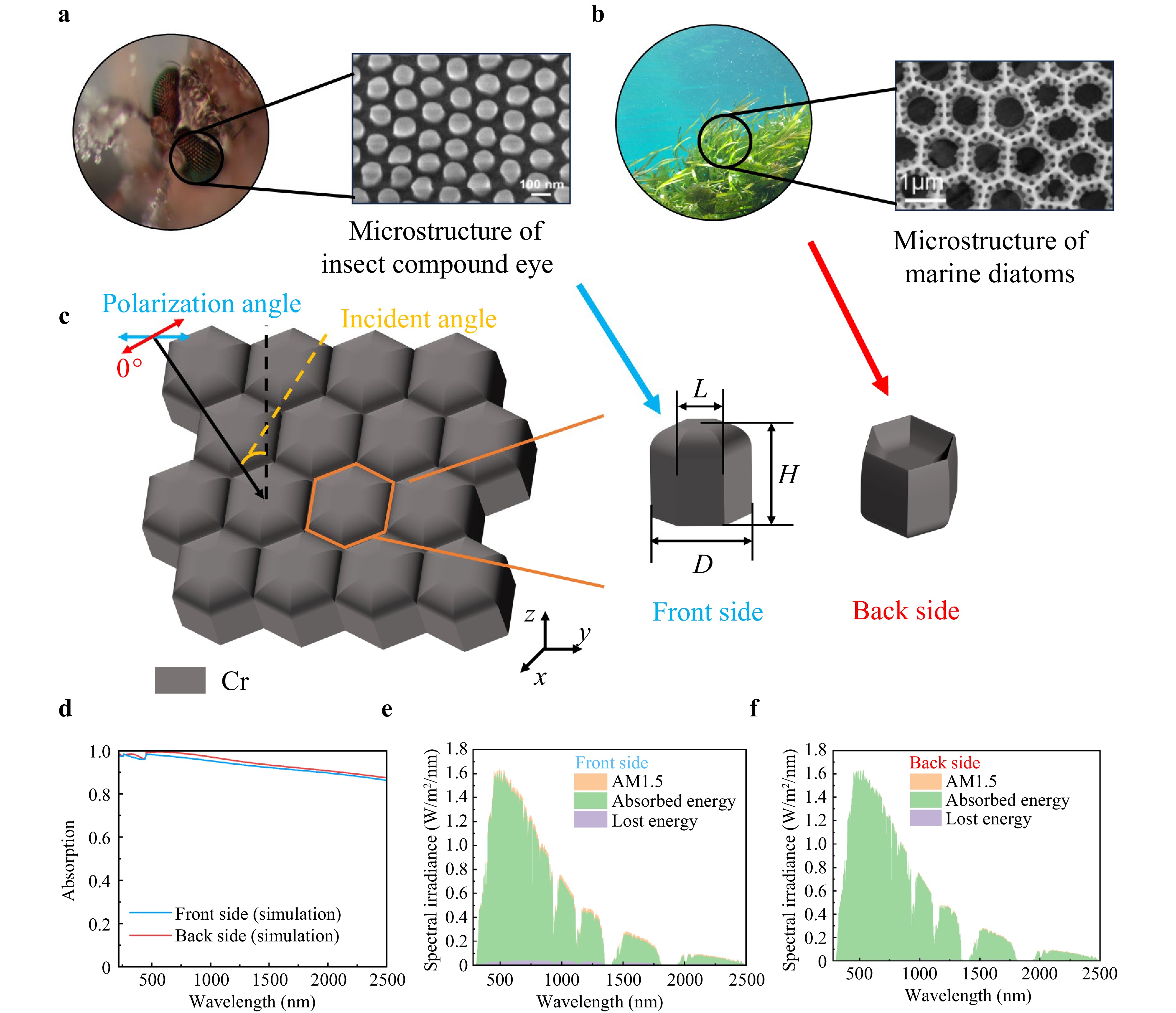
Fig. 1 Structure design and absorption performance. a Microstructure of the moth-eye compound eye.46 Copyright 2007, Wiley. b Microstructure of marine diatoms.36 Copyright 2007, Wiley. c Schematic of the biomimetic metamaterial absorber structure. d Simulated absorption spectrum of the metamaterial absorber. e Simulated absorption and energy loss spectra on the front and f back sides in the AM1.5 solar spectrum.
Chromium (Cr) was chosen as the constituent material because of its large imaginary part in the dielectric function in the ultraviolet to near-infrared region, where terrestrial solar radiation is primarily concentrated. Moreover, compared with noble metals such as gold and silver, chromium offers advantages such as lower cost and more mature fabrication processes, thereby making it more suitable for large-scale applications.
After systematic optimisation (Figure S1, Supporting Information), the optimal structural parameters were determined as P = 520 nm, D = 500 nm, L = 290 nm, and H = 500 nm. Consequently, as shown in Fig. 1d, the simulated average absorption efficiencies of the freestanding Cr nanostructure reach 93% and 94% for front and back-side illumination, respectively. In the AM1.5 solar spectrum, the corresponding average absorption efficiencies further increase to 96% and 98%, respectively, as shown in Fig. 1e, f (the calculation method for the AM1.5 spectrum is provided in Supporting Information S2).
-
To gain deeper insight into the physical origin of the ultrabroadband absorption, electromagnetic simulations were performed to analyse the field distributions of the developed DS-BMA at three representative wavelengths of 500, 1,500, and 2,500 nm. As shown in Fig. 2, the ultrabroadband absorption arises primarily from the synergistic interplay between surface plasmon resonances and magnetic polariton excitations. In addition, the unique gradient geometry, which is characterised by a continuous transition from hemispherical protrusions on the top surface to hemispherical cavities on the bottom surface, facilitates excitation of multiple resonant modes at different wavelengths. Therefore, the absorption bandwidth is effectively extended from the ultraviolet to the near-infrared region. To quantitatively distinguish the contribution of the surface structure from the intrinsic material loss, the optical constants ($ n $ and $ k $) of the sputtered Cr film and absorption spectrum of a 1,000-nm-thick planar Cr film were systematically characterised (Fig. S2, Supporting Information). The planar Cr film exhibited an average absorptance of only 68.1% over the wavelength range of 220–2,500 nm. Although the large extinction coefficient ($ k $) of Cr ensured strong optical dissipation and negligible transmission, it also caused considerable reflection owing to the impedance mismatch at the air/Cr interface. By contrast, the biomimetic micro/nanostructure reduced the reflection loss by a smoother optical transition and promotes multiple light–matter interactions within the structure. Consequently, the average absorptance exceeded 93%. Therefore, the observed near-perfect absorption originates from the synergistic contribution of the intrinsic loss of Cr and structural modulation of the optical field.
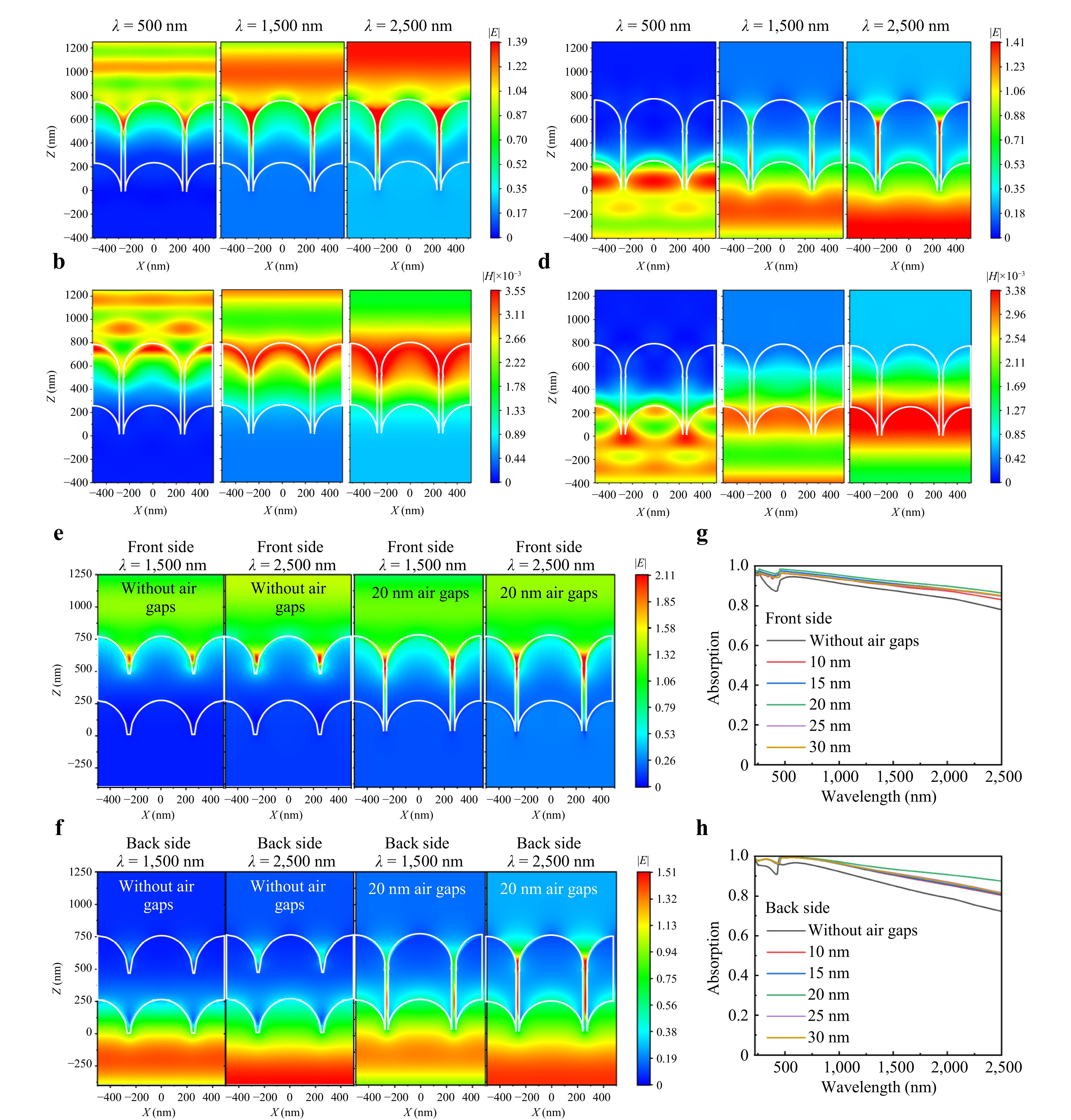
Fig. 2 Electromagnetic response mechanism of the broadband absorption. a Electric field and b magnetic field distributions on the front side of the biomimetic metamaterial absorber at 500 nm, 1,500 nm, and 2,500 nm wavelengths. c Electric field and d magnetic field distributions on the back side at the same wavelengths. e Comparison of the electric field distributions on the front and f back sides of the single-layer Cr structures with a representative nanogap of 20 nm at wavelengths of 1,500 nm and 2,500 nm. g Absorption spectra on the front and h back sides of the single-layer Cr structures with various nanogap sizes (gap = 10, 15, 20, 25, and 30 nm) and reference structure without air gap.
At the shorter wavelength of λ = 500 nm, pronounced electric and magnetic field localisation is observed near the top surface of the structure, as shown in Fig. 2a, b. This indicates excitation of surface plasmon resonances at the chromium–air interface. Enhanced magnetic fields are also detected along the sidewalls of the absorber, which can be attributed to the excitation of magnetic polaritons. These two mechanisms work cooperatively to confine the electromagnetic energy to the upper surface and sidewall regions of the Cr layer. Owing to the intrinsically high optical loss of Cr, the localised electromagnetic energy is efficiently dissipated within the metal, which results in strong absorption in the short-wavelength regime. At the intermediate wavelength of λ = 1,500 nm, the magnetic field enhancement is predominantly concentrated along the sidewall regions (Fig. 2b), which indicates that magnetic polaritons become the dominant absorption mechanism in this spectral range. This magnetic resonance behaviour can be described well using an equivalent LC circuit model (Fig. S3, Supporting Information). In this model, the Cr nanostructure acts as an effective nanoinductor (L), whereas the air gaps between adjacent Cr units and the air-filled recessed regions within the structure serve as effective nanocapacitors (C). Under this framework, the resonance wavelength of the magnetic polaritons can be approximately expressed as $ \lambda \approx 2{\text{π}} {c}_{0}\sqrt{LC} $. Importantly, the complementary gradient geometry leads to wavelength-dependent variations in the effective inductive and capacitive responses along the vertical direction. Consequently, magnetic polariton resonances can be excited at different spatial locations for different spectral ranges, which collectively contribute to the observed ultrabroadband absorption in a single metallic layer. For front-side illumination, the effective capacitance C increases as the interparticle gaps and metal separations decrease along the vertical direction, which leads to a redshift in the magnetic polariton resonance. Consequently, with increasing incident wavelength, the localisation region of the magnetic polaritons gradually shifts downward along the sidewalls. When an electromagnetic wave is incident from the back side, the underlying physical mechanisms remain essentially the same, with surface plasmon resonances and magnetic polaritons still playing dominant roles. The primary difference lies in the composition of the effective capacitance C, which is mainly determined by the air regions enclosed by the hemispherical chromium cavities on the lower surface. This complementary capacitive configuration enables efficient excitation of the resonant modes under reverse illumination, thereby ensuring high absorption from both sides.
Notably, as shown in the comparative simulations in Fig. 2e, f, introducing nanoscale gaps between adjacent polystyrene (PS) spheres significantly enhances the absorption compared with the ideal close-packed structure without gaps. This improvement can be attributed to several factors. First, the nanoscale gaps create a strong capacitive coupling between neighbouring metallic units, which significantly enhances the local electric fields. Second, these gaps electrically isolate adjacent units, thereby enabling the formation of pronounced loop currents that strengthen the magnetic polariton resonances, which are particularly critical for near-infrared absorption. Finally, the presence of nanoscale gaps optimises the overall effective impedance of the structure and improves the impedance matching with free space over a broader spectral range, thereby suppressing reflection more effectively. To further clarify the representative dimensions, a nominal nanogap of 20 nm observed in our experimental samples is adopted for the electric field distributions shown in Fig. 2e, f. Regarding large-area manufacturing controllability, these nanoscale gaps are naturally formed owing to the physical self-limiting nature of sphere packing and subsequent shadowing effect during magnetron sputtering.47 Statistical analysis based on different fabrication batches (Supporting Information Figure S4) showed a relatively concentrated nanogap distribution centred at ~20 nm, which supports the reasonable uniformity of the experimentally observed gap feature. Although this bottom-up approach exhibits minor fluctuations compared with high-precision lithography, the optical performance of the developed metasurface remains highly tolerant to such variations. The parametric simulation results in Fig. 2g, h show that the 20 nm gap delivers the optimal absorption performance, whereas structures with gap sizes ranging from 10 to 30 nm still maintain band-averaged absorptances exceeding 90.8%/91.5% (front/back) in the 220–2,500 nm range. Therefore, these structures with a gap substantially outperform the gapless reference structure (87.9%/86.5%). This broad tolerance window indicates that moderate fabrication-induced gap variations do not severely degrade the broadband light-harvesting capability, thereby reinforcing the robustness and scalability of the developed fabrication strategy.
Because of the highly symmetric geometric design, the absorption spectra remained essentially identical under different polarisation states (Fig. S5, Supporting Information). Moreover, the absorber maintained an average absorption exceeding 80% over a wide incident angle range of 0–60° (Fig. S5, Supporting Information), which exhibits its excellent angular insensitivity. These characteristics render the developed structure particularly suitable for practical light-harvesting applications involving unpolarized and obliquely incident solar radiation.
-
A lithography-free fabrication strategy was developed for the preparation of the metamaterial absorber (Fig. 3a; Fig. S6 and S7 in Supporting Information), which could be flexibly transferred using a transparent PET adhesive tape. As shown in Fig. 3a, first, a highly ordered monolayer array of PS microspheres with a diameter of 500 nm is assembled on a silicon substrate by combining gas–liquid interfacial self-assembly with the Langmuir–Blodgett technique. This method forms a regular two-dimensional photonic crystal template. Subsequently, a 500 nm-thick Cr film is deposited onto the PS template via magnetron sputtering, thereby resulting in a PS–Cr composite structure. After thermal treatment at 400 °C for 2 h to remove the PS template, the metamaterial absorber is non-destructively transferred using a PET adhesive tape. The PET adhesive tape exhibits excellent flexibility, thereby endowing the transferred absorber with outstanding bending tolerance. Its high optical transparency and reliable adhesion preserve the intrinsic optical properties of the metamaterial in the visible to near infrared wavelength range (Text S8 in the Supporting Information) while ensuring stable attachment to various target substrates. This fabrication approach, which integrates template-assisted patterning with flexible transfer technology, offers a versatile route for applying metamaterial absorbers to curved optical components and wearable devices. In this study, this approach was implemented on samples with dimensions of up to 2 cm × 2 cm, which was the maximum size achievable using the current laboratory setup. However, similar gas-liquid interfacial self-assembly methods have been extended to wafer-scale fabrication, which indicates the scalability potential of the underlying assembly strategy45.
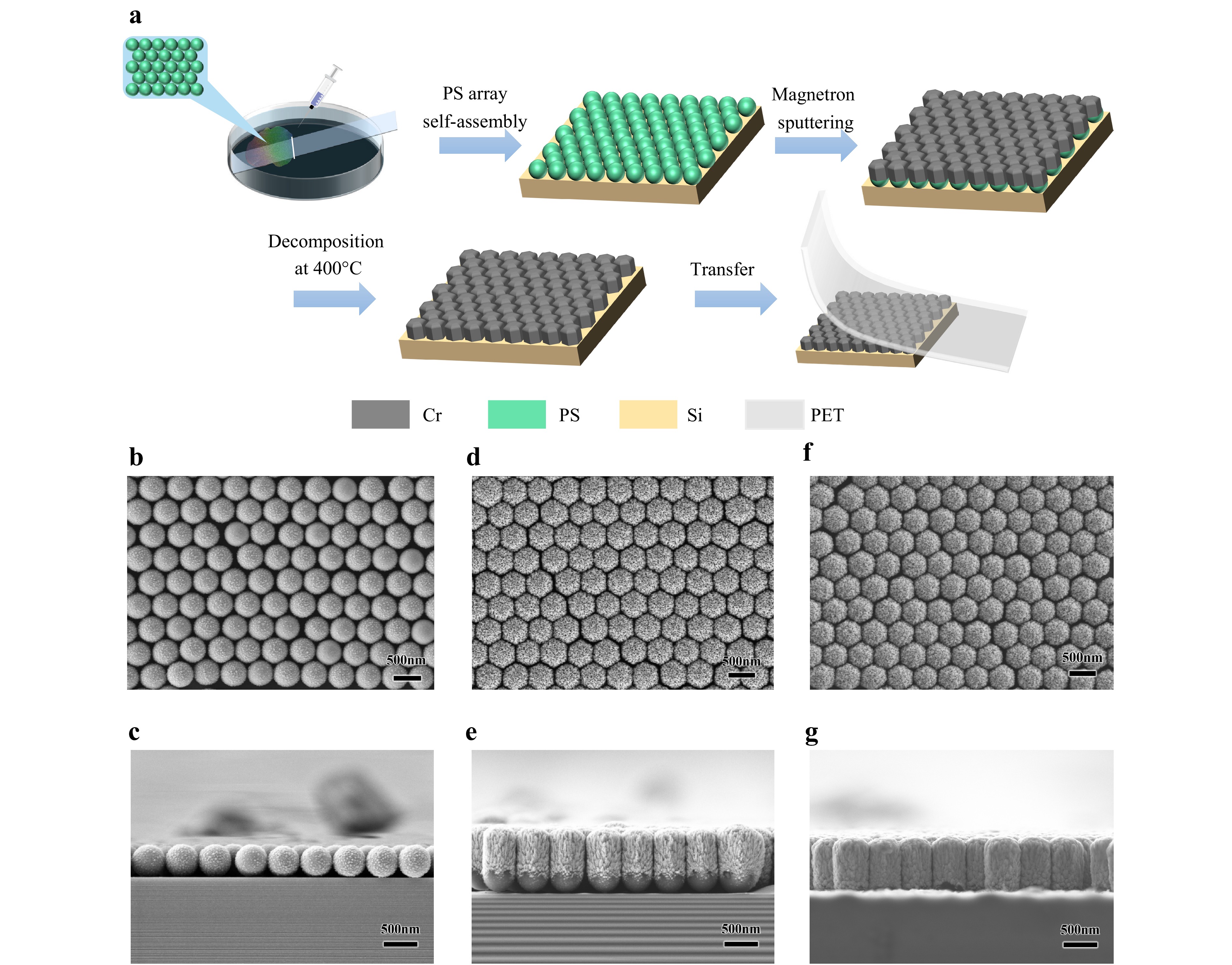
Fig. 3 Fabrication process and structural characterization. a Schematic of the fabrication process of the biomimetic metamaterial absorber. SEM images of a b, c single-layer periodic PS microsphere array, d, e PS array after Cr deposition, and f, g DS-BMA sample.
The surface morphologies of the samples were characterised using scanning electron microscopy (SEM), and SEM images are shown in Fig. 3b, g and Fig. S8 (Supporting Information). Because of the intrinsic characteristics of magnetron sputtering and monolayer PS microsphere template, nanoscale gaps of approximately 20 nm are formed between adjacent microspheres. Although such gaps are generally regarded as unavoidable microstructural imperfections in experiments, the preceding mechanism analysis indicates that these nanoscale gaps enhance light scattering and electromagnetic confinement, thereby improving the overall optical absorption performance. In addition, owing to the relatively large size of the Cr clusters generated during direct-current sputtering, the deposited Cr layer exhibits a discontinuous morphology. Compared with continuous metallic films, discontinuous chromium structures generally possess higher optical absorption and reduced intrinsic film stress, which significantly improves the success rate of the subsequent transfer process. Collectively, these structural features lead to the efficient light harvesting and robust flexible transfer of the metamaterial absorber.
-
The absorption of the fabricated DS-BMA was measured using an ultraviolet–visible–near-infrared spectrophotometer. As shown in Fig. 4a, the absorber exhibits outstanding broadband near-perfect absorption in the 220–2,500 nm, with measured average absorption efficiencies of 93.8% and 96.1% for front- and back-side illumination, respectively. These experimental results are in excellent agreement with the simulated predictions, thereby validating the effectiveness of the developed design. As shown in Fig. 4b-d, systematic characterisation further exhibits that the absorber maintains high absorption under different polarisation states. Moreover, stable absorption performance occurs over a wide incident angle range of 0–60°, thereby confirming the excellent polarisation-insensitive and wide-angle absorption characteristics of the device. In addition, the absorption performance in the standard AM1.5 solar spectrum was evaluated using the measured spectra. As shown in Fig. 4e, f, the average absorption efficiencies reach 94% and 96% for front- and back-side illumination, respectively, which highlights the significant potential of the absorber for efficient solar energy harvesting and photothermal utilisation. Supporting Information Table S1 summarises the key performance metrics of representative broadband absorbers reported in recent literature. Compared with these broadband absorbers, our device simultaneously exhibits a broader effective absorption bandwidth and higher average absorptance over the solar spectrum. Near-perfect absorption exceeding 93% is achieved on both the front and back sides throughout the ultraviolet-visible-near-infrared region. Compared to most previously reported structures, which realise high absorption only under single-sided illumination or within limited spectral ranges, the developed single-layer DS-BMA offers clear advantages in terms of the absorption bandwidth, dual-sided absorption symmetry, and structural simplicity. Moreover, the developed absorber does not rely on complex multilayer stacking or sophisticated lithographic processes and still exhibits excellent flexibility and transferability together with a strong potential for large-area fabrication. Therefore, it is superior to existing broadband absorbers in terms of overall performance and practical applicability.
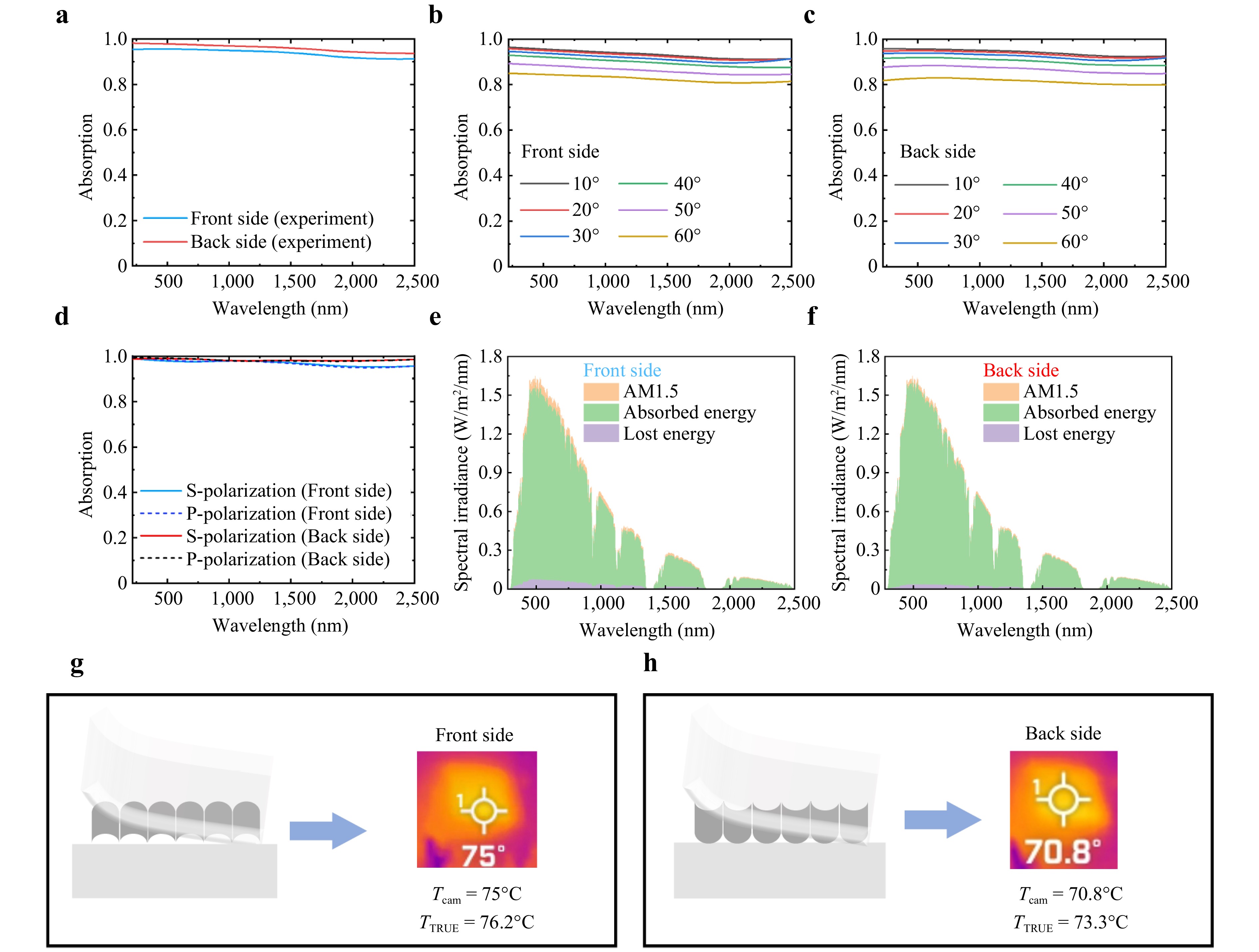
Fig. 4 Broadband absorption characterization. a Absorption spectra of the DS-BMA sample under normal incidence. b Absorption spectra for the front and c back sides of the DS-BMA at different incident angles. d Absorption spectra under polarized light. e Absorption spectra for the front and f back sides in the AM1.5 solar spectrum. g The temperature of the front and h back sides of the DS-BMA absorber in thermal equilibrium under 1 sun.
To further evaluate the photothermal conversion capability of the DS-BMA, photothermal heating experiments were performed under standard one-sun illumination (AM1.5, 1,000 W·m−2). A calibrated solar simulator was employed to ensure spatially uniform and temporally stable irradiation. The use of a standard one-sun condition eliminated regional and seasonal variations in the natural solar irradiance, thereby providing a reproducible and location-independent evaluation platform48. To minimise conductive heat loss and accurately capture the true thermal equilibrium, a flexible sample was suspended in ambient air using a minimal metal frame support and avoiding any direct contact with solid surfaces that could act as thermal sinks. The front and back sides of the sample were separately exposed to identical irradiation conditions. Starting from room temperature (25 °C), the sample heated rapidly and reached a steady-state equilibrium after approximately 15 min. A precise radiometric calibration based on the experimentally measured mid-infrared emissivity spectra was performed (detailed in Supporting Information S12). As shown in Fig. 4g, h, the true equilibrium temperatures reach 76.2 °C and 73.3 °C under front- and back-side illumination, respectively. Notably, once equilibrium is reached, the temperatures remain nearly constant for more than 90 min under continuous one-sun irradiation, which shows excellent photothermal stability. The comparable temperature rise under front- and back-side illumination further confirms the effective dual-sided solar absorption and efficient light-to-heat conversion capability of the DS-BMA, which highlights its strong potential for solar-driven photothermal applications (see Supporting Information S12 for a detailed analysis).
-
To evaluate the reliability of the double-sided absorber under practical operating conditions, comprehensive environmental and mechanical stability tests were conducted; the specific test data are listed in Table 1. Owing to the flexible PET-based encapsulation and transfer layer, the absorber can be conformally laminated onto nonplanar or flexible surfaces, including curved, folded, or slightly textured substrates, without inducing structural damage or performance degradation, as shown in Fig. 5a. The PET provides sufficient mechanical support to accommodate bending and deformation while simultaneously serving as a protective barrier that shields the Cr nanostructures from direct chemical and physical damage. This combination enables robust integration of the absorber into complex application scenarios.
Test methods Measured Band-averaged Absorption over 220–2,500 nm Illumination side Before (%) After (%) Absolute change (%) Corrosion resistance(24 h immersion in sulfuric acid) Front side 93.78 93.31 −0.47 Back side 96.06 94.33 −1.74 Thermal stability(150 °C, 5 h) Front side 93.78 93.69 −0.09 Back side 96.06 98.65 +2.59 Bending durability (500 cycles) Front side 93.78 93.65 −0.13 Back side 96.06 96.32 +0.25 Table 1. Summary of the stability tests of the double-sided absorber
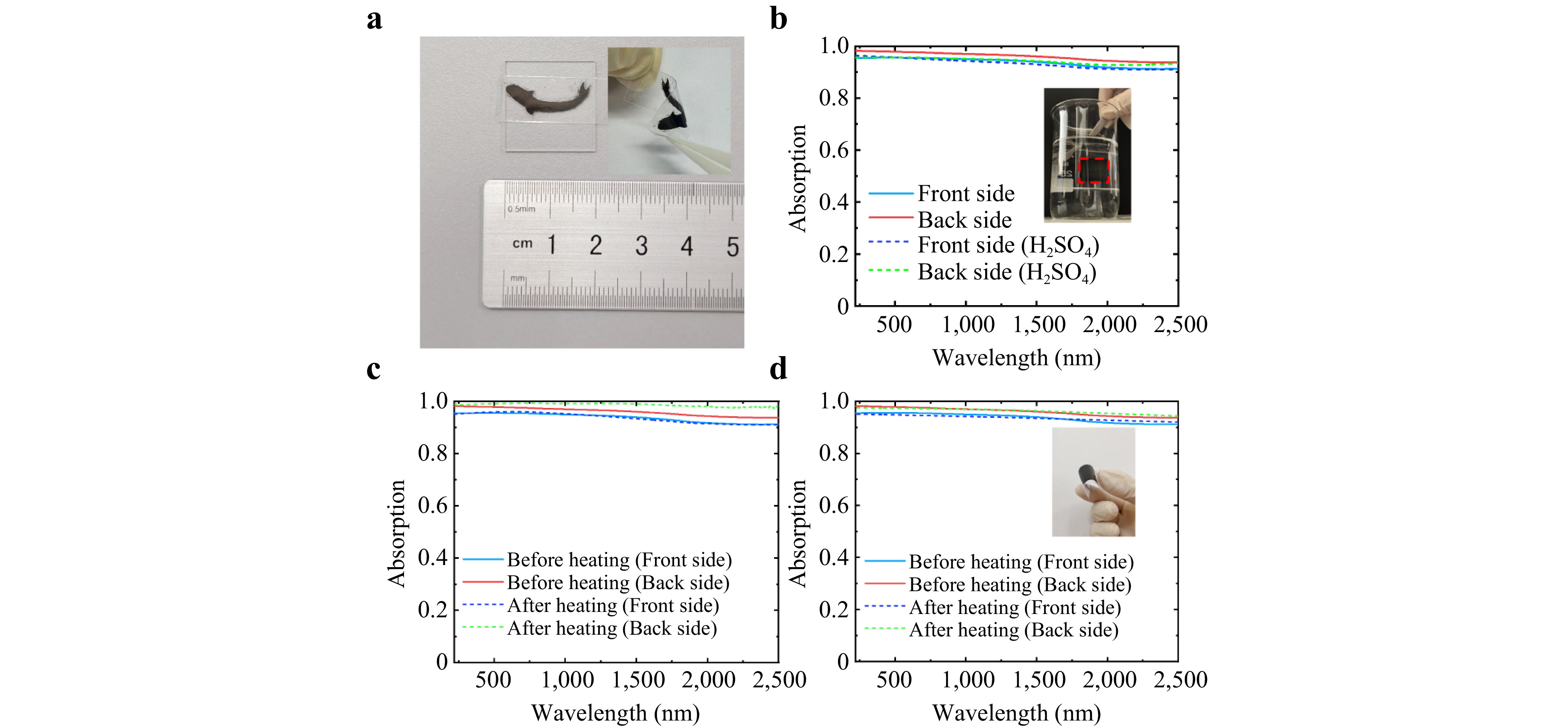
Fig. 5 Performance stability under different environments. a Images of the DS-BMA after patterning. Absorption spectra of the DS-BMA before and after b corrosion resistance test, c thermal stability test at 150 °C, and d mechanical bending durability test for 500 cycles.
Corrosion resistance was evaluated by immersing the encapsulated device in a highly concentrated sulfuric acid solution (18 mol·L−1) for 24 h. As shown in Fig. 5b, after exposure, the absorber maintains its structural integrity and optical performance. The band-averaged absorptance over the wavelength range of 220–2,500 nm decreases only slightly from 93.78% to 93.31% for front-side illumination and from 96.06% to 94.33% for back-side illumination (Fig. 5b), corresponding to absolute variations of 0.47% and 1.74%, respectively. These results show the excellent chemical stability and corrosion resistance of the encapsulated DS-BMA in harsh acidic environments.
Thermal stability was assessed by conducting accelerated aging tests at 150 °C for 5 h. This temperature was selected by considering the high melting point of Cr (~1,800 °C) and thermal tolerance of the current encapsulation tape (~200 °C). As shown in Fig. 5c, the broadband absorption performance remains stable after heating. The band-averaged absorptance over 220–2,500 nm exhibits only a negligible decrease of 0.09% for front-side illumination, whereas the back-side absorptance shows a slight increase of 2.59%, indicating excellent thermal robustness of the absorber. Notably, the operational temperature limit of the device can be further extended by employing encapsulation materials with a higher thermal endurance.
The mechanical stability was further examined by conducting bending durability tests over 500 bending cycles. As shown in Fig. 5d, the band-averaged absorptance remains essentially unchanged after repeated mechanical deformation, with variations of only 0.13% for front-side illumination and 0.25% for back-side illumination. These negligible changes confirm the excellent mechanical robustness of the double-sided absorber and show that its ultrabroadband absorption performance is preserved well under repeated bending and deformation.
-
We developed a single-layer double-sided biomimetic metamaterial absorber tailored to the solar spectrum. Owing to the synergistic effects of surface plasmon resonances and magnetic polariton excitations, the absorber achieves excellent broadband absorption over the wavelength range of 220–2,500 nm, with average absorption efficiencies of 93% and 96% for front-side and back-side illumination, respectively. Because of its simple structural configuration, compatibility with manufacturing fabrication, and flexible transferability, the developed absorber can be readily adapted to diverse application scenarios. The device exhibits omnidirectional polarization-insensitive absorption, outstanding thermal stability, corrosion resistance, and mechanical robustness, thereby ensuring reliable operation under complex environmental conditions. Importantly, beyond Cr, other low-cost metals with high intrinsic optical losses, such as titanium, may also achieve comparable broadband absorption performance by appropriate structural optimisation, thereby providing additional flexibility for material selection in future studies. These features render the developed absorber highly attractive for applications requiring efficient double-sided light capture and a broadband spectral response, including bifacial photovoltaic devices, solar-driven interfacial desalination systems, and emerging multifunctional photothermal regulation platforms.
-
Monodisperse PS microspheres with a diameter of 500 nm were purchased from Shanghai Huizhi Biotechnology Co., Ltd. Sodium dodecyl sulphate (SDS) was obtained from Shanghai Beyotime Biotechnology Co., Ltd. High-purity Cr sputtering targets were supplied by Zhongnuo Advanced Material (Beijing) Technology Co., Ltd. The transparent adhesive tape used for the transfer consisted of polyacrylate adhesive and PET backing layers and was purchased from Foshan Xinfengshang New Materials Technology Co., Ltd. All the materials were used as received without further purification.
-
A PS microsphere monolayer mask was prepared via gas-liquid interfacial self-assembly. Briefly, 0.1 mL of aq. 5 wt% suspension of 500 nm PS microspheres was diluted with anhydrous ethanol at a volume ratio of 1:2 and ultrasonicated for 60 s to obtain a uniformly dispersed suspension. A rectangular glass substrate was then placed obliquely (≈30°) in 400 mL of deionised water, followed by addition of 20 μL of 10 wt% SDS solution to reduce the surface tension of the aqueous phase. After stabilization of the water surface, the PS microsphere suspension was slowly injected along the inclined glass substrate into the water phase at a constant rate of 0.4 μL·s−1 using a microsyringe pump. Driven by the Marangoni effect at the air–water interface and surfactant action of SDS, the PS microspheres spontaneously assembled into a highly ordered hexagonally close-packed monolayer at the water surface. The assembled monolayer was subsequently transferred onto a 2 cm × 2 cm silicon substrate using the Langmuir–Blodgett technique and allowed to dry naturally.
-
Cr was deposited using a high-vacuum magnetron sputtering system (ATTO 10). The PS microsphere monolayer samples were fixed on a sample holder and aligned parallel to a Cr target with a purity of 99.99%. After the base pressure of the chamber reached 5 × 10⁻⁵ Pa, high-purity argon gas (99.999%) was introduced at a flow rate of 20 sccm to maintain a working pressure of 6.8 × 10⁻² Pa. Direct-current sputtering was performed at 50 W for 1 h at 25 °C, which yielded a Cr layer with a thickness of approximately 500 nm. The PS microsphere mask was subsequently removed by thermal treatment. Specifically, the samples were placed in a tube furnace (CAD) and heated to 400 °C at a ramping rate of 9 °C min−1 under an argon flow of 500 sccm, followed by annealing for 2 h to ensure complete decomposition of the PS spheres. The samples were naturally cooled to room temperature, which yielded a pure Cr layer with periodic micro/nanostructures.
-
A transparent PET adhesive tape was employed as the transfer medium for efficient transfer and encapsulation of the metamaterial absorber. Specifically, the PET tape was gently laminated onto the fabricated absorber surface under moderate pressure to ensure intimate contact, followed by slow peeling to completely transfer the absorber onto the tape. The transferred absorber was attached to the desired target substrate. This simple transfer process effectively preserved the structural integrity and optical performance of the absorber, thereby enabling its facile integration onto substrates with various shapes.
-
The microstructural morphology of each fabricated metamaterial absorber was characterised using field-emission SEM (FESEM; ZEISS Ultra 55). The optical properties were measured using an ultraviolet-visible-near-infrared spectrophotometer (SolidSpec-3700, Shimadzu) over a wavelength range of 220–2,500 nm, from which the reflectance and transmittance spectra were obtained. All the optical measurements were conducted at room temperature.
-
Numerical simulations were performed using the finite-difference time-domain method to investigate the optical response of the metamaterial absorber. Because the PET transfer layer was not part of the original absorber design, it is not included in the simulations described in the main text. Additional simulations incorporating the PET layer are discussed in Supporting Information S8. The results showed that it mainly functions as a mechanically supportive and protective encapsulation layer and introduces only a minor optical contribution within the investigated spectral range. The optical constants (refractive index n and extinction coefficient k) of Cr were obtained from experimentally measured ellipsometry data to ensure accurate material modelling. According to the law of energy conservation, absorption (A) was calculated as A = 1 − R − T, where R and T denote the reflectance and transmittance, respectively. Periodic boundary conditions were applied in the x- and y-directions to simulate an infinite periodic array, whereas perfectly matched layer boundary conditions were used along the z-direction to eliminate nonphysical reflections. The spatial mesh resolution of the simulation region was set to 4 nm.
-
This work was supported by the Natural Science Foundation of Guangdong Province (2024A1515012296 and 2025A1515011712) and the Guangzhou Municipal Science and Technology Project (2019050001). The authors gratefully acknowledge Dr. Huanzheng Zhu of Zhejiang University for his valuable assistance in mid-infrared spectral measurements.
Single-layer double-sided ultrabroadband absorber based on biomimetic metamaterial with manufacturing scalability
- Light: Advanced Manufacturing , Article number: 120 (2026)
- Received: 02 April 2026
- Revised: 02 July 2026
- Accepted: 03 July 2026 Published online: 18 September 2026
doi: https://doi.org/10.37188/lam.2026.120
Abstract: Efficient light harvesting from front and rear sides is essential for improving solar energy utilisation in applications such as photovoltaics and seawater desalination. This requires absorbers that exhibit strong double-sided absorption in the ultraviolet to near-infrared range, mechanical flexibility for transfer onto diverse substrates, reliable performance stability, and manufacturing scalability for practical deployment. However, these capabilities are difficult to achieve simultaneously using conventional thin-film or metamaterial absorbers. In this study, we developed a double-sided bioinspired metamaterial absorber (DS-BMA) composed of a single layer of chromium (Cr) nano-units, whose front and back surfaces mimic the morphologies of moth eyes and marine diatoms, respectively. The gradient geometric configuration of the DS-BMA significantly broadened the bandwidths of plasmonic resonances, thereby enabling near-perfect absorption over the entire solar spectrum. Using a scalable self-assembly-based process, we experimentally showed a flexible, transferable DS-BMA with a thickness of 500 nm. It achieved average absorptances of 93% and 96% on the front and back sides, respectively, over a wavelength range of 220–2,500 nm. The DS-BMA exhibited polarisation-independent omnidirectional absorption as well as excellent thermal stability, corrosion resistance, and mechanical robustness. Therefore, the DS-BMA provides a promising route toward high-efficiency, low-cost, and integrable photothermal/photovoltaic energy conversion devices.
Research Summary
Bioinspired double-sided metamaterial absorber for full-spectrum solar harvesting
To achieve efficient double-sided light harvesting for photovoltaics and seawater desalination, an absorber should combine strong broadband absorption, flexibility, stability, and scalability—qualities lacking in conventional designs. Yihang Chen from South China Normal University, China, Meiyan Pan from Ji Hua Laboratory, China, and their colleagues developed a single-layer, bioinspired metamaterial that absorbs light from both sides with near-perfect efficiency across the entire solar spectrum. Mimicking moth eyes on one surface and marine diatoms on the other, the 500-nm-thick flexible film achieves average absorptances of 93% and 96% from front and back, respectively, over 220-2500 nm. Fabricated via scalable self‑assembly and sputtering, it withstands bending, heat, acid, and long‑term exposure, while maintaining polarization‑independent and wide‑angle performance. This design offers a practical pathway toward high‑efficiency, low‑cost, and integrable solar energy conversion systems.
Rights and permissions
Open Access This article is licensed under a Creative Commons Attribution 4.0 International License, which permits use, sharing, adaptation, distribution and reproduction in any medium or format, as long as you give appropriate credit to the original author(s) and the source, provide a link to the Creative Commons license, and indicate if changes were made. The images or other third party material in this article are included in the article′s Creative Commons license, unless indicated otherwise in a credit line to the material. If material is not included in the article′s Creative Commons license and your intended use is not permitted by statutory regulation or exceeds the permitted use, you will need to obtain permission directly from the copyright holder. To view a copy of this license, visit http://creativecommons.org/licenses/by/4.0/.

 DownLoad: