


-
Over the years, the use of lasers has led to differentiated operations capable of supporting material patterning, transfer, and synthesis, catering to many niche applications involving material refinement and device production. With worldwide advancement in technology, the economies of scale in the production of lasers have yielded widespread adoption of laser systems at reasonable costs. The ubiquity of lasers, incorporated either as components to specialized optical instruments or flexibly coupled to standalone optical microscopes, have encouraged facile and convenient operations in material production, modification, and characterization. Along with the growing demand for rapid and simpler operations, the competing role of lasers in materials research has prompted the birth of multiple techniques, including laser-induced forward transfer1, 2, laser synthesis and processing of colloids (LSPC (Fig. 1a)), including laser ablation in liquids (LAL)3–7, laser fragmentation in liquids (LFL)8, and laser melting in liquids (LML)9, 10, laser-assisted additive manufacturing11, laser-assisted chemical vapor deposition (LCVD), pulsed laser deposition (PLD)12–15, nanolithography16, direct laser writing17–21, pruning (Fig. 1b)22, sintering23, microprinting24, and patterning (Fig. 1c, d)25–31. Based on the multiple parameters available in shaping the laser beam characteristics, the role of lasers permitted systematic investigation on the laser-induced restructuring of material properties, shedding light on many novel optical phenomena across a myriad of nanomaterials.
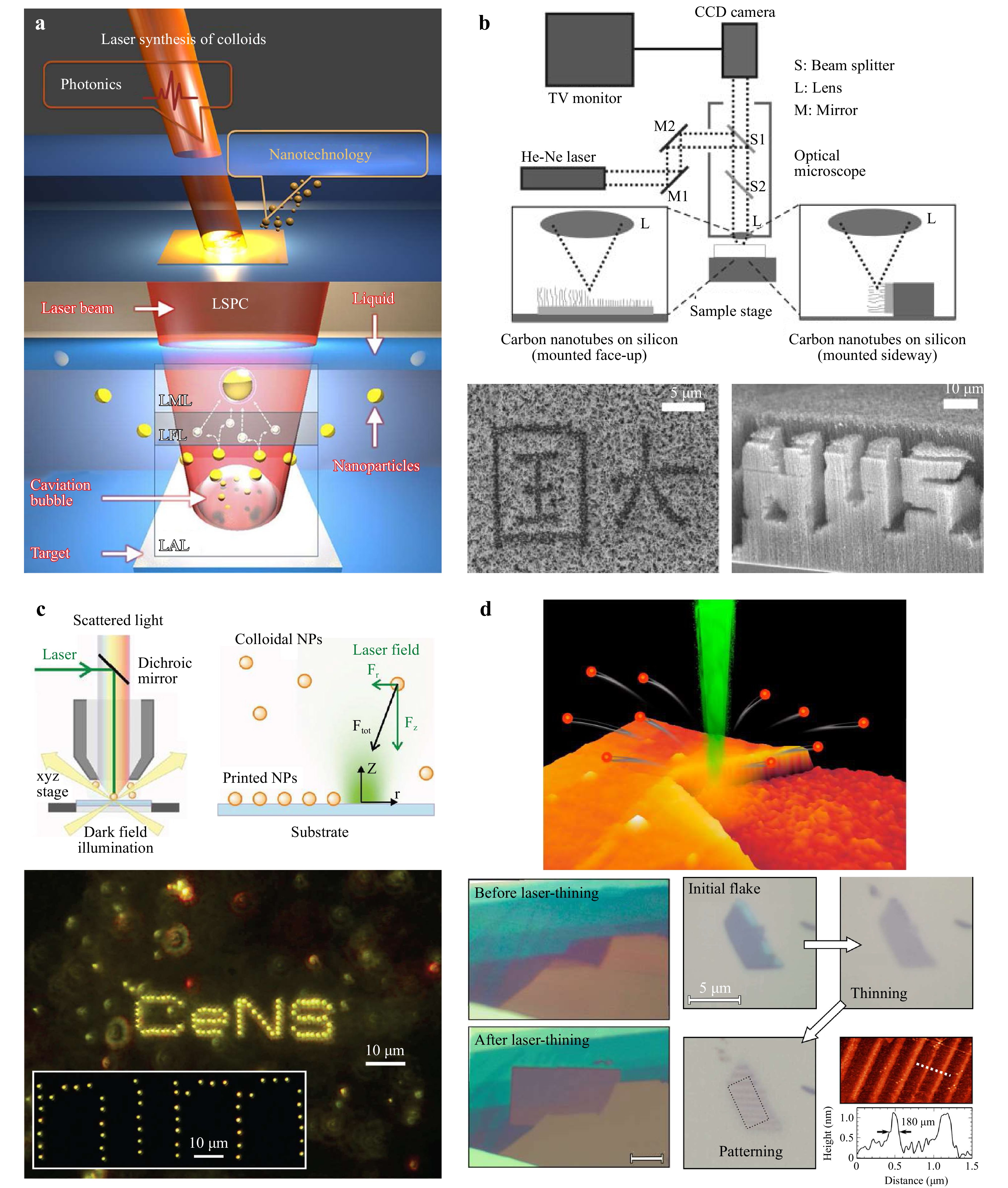
Fig. 1 Demonstration of laser operation modes for materials research. a Laser synthesis and processing of colloids (LSPC) are detailed into LAL, LFL, and LML regions. Reproduced with permission from ref. 5 Copyright 2017 American Chemical Society. b Laser pruning of vertical carbon nanotube arrays. Schematic of the laser setup used to produce the micro-structures. Reproduced with permission from ref. 22 Copyright 2003 Wiley-VCH. c Direct laser printing of individual colloidal gold nanoparticles. Reproduced with permission from ref. 25 Copyright 2010 American Chemical Society. d Laser thinning process on multilayer MoS2 to produce monolayers and patterned regions. Reproduced with permission from ref. 31 Copyright 2012 American Chemical Society.
Luminescence in nanomaterials, particularly in the domains of downshifting fluorescence (hereafter referred to as fluorescence) and upconversion emission, has been highly sought after for their value in bioimaging32–35, quantum light emitters36–38, light-emitting electronics39–43, and micro-encryption patterns44–48. For instance, classical examples of fluorescence quantum dots comprising II-VI/III-V semiconductors49–54, carbon quantum dots (C-dots)55, 56 or perovskite57, 58 nanomaterials have provided the capability for size-modulated fluorescence applicable to these technologies. With tunable bandgaps and π-electron conjugation (C-dots) by modulating the extent of the quantum confinement effect, ease in multicolor adjustments has been achieved. Similarly, the fine-tuning of upconversion emission profile in lanthanide-doped upconversion nanoparticles (UCNPs)59–63 has also provided access to multicolor control across the color gamut. By leveraging ladder-like energy levels in rare earth lanthanide dopants, rational designs of energy transfer dynamics within insulator matrices allow multiphoton upconversion to drive visible emissions from near-infrared (NIR) excitations.
Beyond such systems, defect-state emissions arising from dopant energy levels or F-center recombinations in transparent insulator hosts (oxides, ceramics, etc.) are essential contributors to the expansive constitution of optical nanosystems as well. With 2D transition metal dichalcogenide (TMD) semiconductors, the unique band structure evolution with declining layer count presents yet another peculiar member of the family of fluorescent nanomaterials, optically active only at the monolayer limit64. Generally, these major classes of nanomaterials have instigated invested efforts into full comprehension of their optical physics (charge recombination dynamics, exciton physics, de-excitation process, and photonic correlation) to enhance the performance favorable towards advanced photonic applications. Furthermore, with the implementation of lasers in materials studies, the appended optical probe presents greater revelation into the fluorescence characteristics through thermal, optical, and chemical influences.
Herein, we present a review of the massive database of previous studies involving attempts to influence nanomaterial fluorescence through laser irradiation. The report effectively segregates into the sub-sections of laser-induced fluorescence, laser-modified fluorescence, and laser-assisted patterning of fluorescent materials. In the first section, the fluorescence emission from the laser-induced formation of nanostructures through assorted means of ablation, aggregation, fragmentation, or redox will be discussed. In coherence, the same section incorporates works involving the activation of nanomaterial fluorescence via laser influence. The conversion from a non-emitting form to a luminescent state typically involves either material redox reactions or alterations in nanomorphology. The subsequent section addresses laser-modified fluorescence, in which the laser effect causes a transformation in the original photoluminescence (PL) profile of the nanomaterial. The effect ranges from major spectral readjustments to minor modulations in intensity or weighted ratios between excitonic species. Beyond the intended laser modifications, a brief analysis of unintended laser influence, coming from the inherent laser probe source of the instrumentation, on the dynamic photophysics of 2D materials is also discussed. Finally, the third sub-section describes the involvement of lasers in patterning pre-formed luminescent nanomaterials through disparate mechanisms to yield spatially controlled colored platforms. In summary, an outlook on the potential and flexibility of laser systems to address the recent challenges of nanomaterial research is discussed.
-
Based on the various laser-based techniques introduced above, the capability of lasers to produce fluorescent nanomaterials typically depends either on the physical means of laser influence (optical, thermal) or the initiation of chemical processes via an energy input. The laser's additional optical or thermal input effectively overcomes the activation barriers for material transformation in liberation of its fluorescence functionalities. Furthermore, with flexible control over the laser parameters (power, intensity, area, and duration), the dimensions and morphology of nanomaterials can be refined through the laser process as an indirect manipulation of the resultant fluorescence profile.
For instance, using a nanosecond laser, Onwudiwe et al. presented a laser-localized decomposition of a chemical precursor (Cd(II) bis(N-ethyl-N-phenyl dithiocarbamate)) in the production of CdS nanoparticles in a polyvinyl alcohol polymer matrix. The ability to correlate nanoparticle dimensions with the accorded substrate temperature reflects quality control over the absorption and PL profiles owing to evolving quantum confinement effects65. Similarly, Seah et al. presented a laser-catalyzed degradation of aqueous aluminum nitrate in the presence of graphene oxide (GO), producing patterns of blue fluorescence originating from aggregate masses of C-doped Al2O3 sub-micron particles (Fig. 2a)66. Simply with the modulation in laser parameters and precursor concentrations, disparate aggregate sizes and distribution uniformities were acquired, presenting optimization handles to the fluorescence intensity achieved.
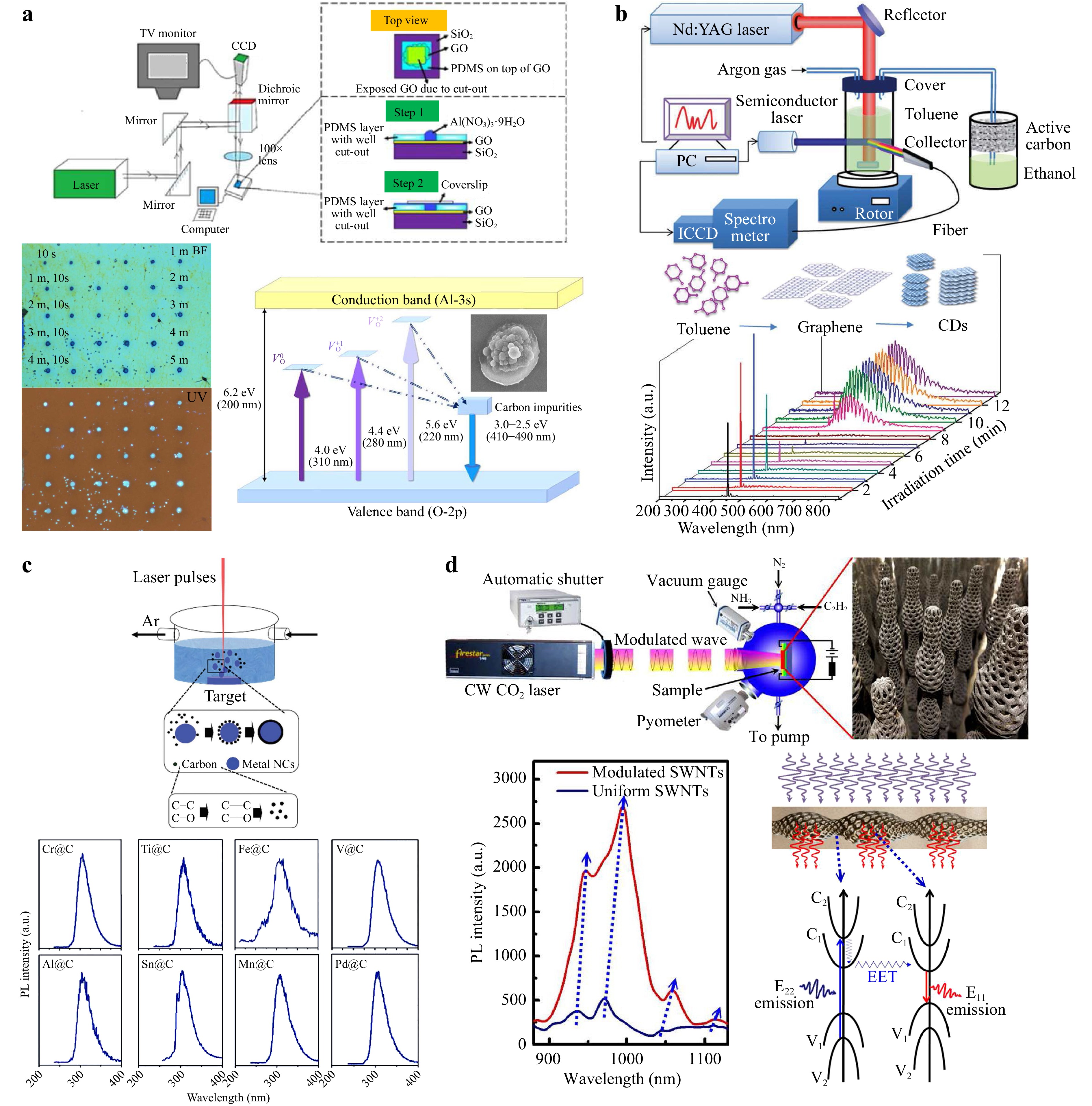
Fig. 2 Laser ablation and laser redox for production of fluorescent nanostructures. a Selective production and deposition of aluminum oxide nanoparticles on a GO platform with carbon defects-driven blue pattern fluorescence. Reproduced with permission from ref. 66 Copyright 2019 Elsevier. b Unfocused laser irradiation upon a toluene solvent to form C-dots of tunable size. Reproduced with permission from ref. 70 Copyright 2016 Royal Society of Chemistry. c Formation of metal@carbon nanoparticles from LAL for deep UV LSPR and PL features. Reproduced with permission from ref. 71 Copyright 2017 Royal Society of Chemistry. d LCVD synthesis of single-walled carbon nanotubes with an alternating width thickness for exciton energy transfer for enhanced PL emission. Reproduced with permission from ref. 75 Copyright 2012 American Institute of Physics.
Operating on an identical method, Lim et al. demonstrated the construction of a hybrid nanostructure consisting of silver nanoparticles (Ag NPs) covered by a layer of alumina veil67. The sequential laser-induced photothermal reduction of silver and aluminum nitrates in the presence of a GO substrate yielded the hybrid with broadband PL emission. With metal-enhanced fluorescence and selective e-beam post-irradiation strengthening of the shorter wavelength emissions, the nanohybrid was proven to be ideal for steganographic transmission. In an operation with greater complexity, Lim et al. also extended the technique to nanocomposite formation (Ag/Ag2MoO4) involving multistep procedures68. After the initial laser pre-patterning of Ag NPs on the GO surface, the patterned distribution provided the basis for the catalytic growth of Ag-doped MoO4 nanowires at the designated locations, simply from hotplate vaporization of an underlying Mo foil. The resultant nanostructure was bright red under UV excitation, presenting a corresponding broadband PL spectrum mediated by localized surface plasmon resonance (LSPR) and incorporated C defect states.
Recently, the class of C-dots has also gained attention as non-toxic, low-cost, stable fluorescent dots synthesized using facile laser ablation techniques69. Conveniently, Yu et al. demonstrated the direct formation of C-dots by irradiating a non-focusing pulsed laser upon a toluene solvent. The solvent precursor transforms through a graphene nanosheet intermediate before the formation of the final graphitic C-dots, continuously monitored through the emergence of its fluorescence (Fig. 2b)70. Employing laser-synthesized carbon as a nanoparticle shell layer, Yu et al. fabricated metal@carbon nanoparticles through the convenient laser ablation of various metal targets in the presence of organic solvents (MeOH/EtOH) as carbon sources (Fig. 2c)71. The carbon shell stabilization of the core metallic nanoparticles resulted in a designed UV LSPR that enhanced the emission of the carbon shells within the UV-blue range. In addition, the production of fluorescent graphitic C-dots was demonstrated by Castro et al. via laser ablation of exfoliated graphite within numerous ionic liquids72 and a polyethylene glycol solvent73. The broadband PL was found to display λmax, peak distribution, and intensity, which differed with varying passivating ligands and counterions. Such associated correlations were expected to arise from the different charge trapping surface states established, along with the potential variation in the quantum confinement extent and influence of the defect states. A similar set of mechanistic factors was found to induce a PL redshift and intensity reduction in laser-fragmented multilayer MoS2 nanosheets presented by Mahdavi et al.74 With laser reduced dimensions, the nanosheets adopted wide bandgap and PL emission characteristics of smaller nanosheet forms, presenting a heavy dependence on the size-determining power of the fragmentation laser source. In an alternate mode of laser-based material production, Samani et al. performed LCVD to craft single-walled carbon nanotubes with segments of alternating diameter thickness by modulating the laser beam into segmented pulse widths (Fig. 2d)75. The regions of differential thickness are characterized by differing bandgap magnitudes, prompting an efficient exciton energy transfer to yield enhanced PL owing to exciton confinement and recombination at the quantum dot-like sections of narrower bandgaps.
Apart from the laser synthesis of the desired fluorescent nanostructures, the ability of the focused laser beam to initiate nanomaterial fluorescence was also achieved through laser-influenced alterations in the surface and defect chemistry of the system. The activation and formation of localized emissions advocate the use of such laser-modified nanostructures for high-resolution micro-patterns, quantum emitters, encryption, and steganographic technologies. Specifically, the approach of laser-thinning nanomaterials is of great significance. Leveraging on the unique layer-dependent indirect-to-direct bandgap conversion in various 2D TMDs, recent explorations into the phenomenon have conferred value to laser techniques used for refined bandgap engineering and controlled fluorescence in such ultrathin materials. Pioneering efforts by Gomez et al.31 and Lu et al.76 demonstrated laser thinning of mechanically exfoliated and CVD-grown MoS2 crystals, respectively. The laser process sublimated the upper MoS2 layers, resulting in thinner 2D crystals with an improved electrical response. With ensuing works, a similar laser thinning process was utilized by Hu et al.77 on MoS2 multilayers and Li et al.78 on graphene combustion to correlate sample thickness with various characterization features. Only in subsequent works by Lu et al.79 and Gong et al.80, were the bulk thinning of the respective WSe2 and MoS2 characterized by their monolayer PL. Gong et al. further administered post-laser self-assembly of gold nanoparticles (Au NPs) on the laser-thinned domains, amplifying the fluorescence in display of the capability of the modified material towards ultrathin optoelectronics. The selective self-assembly process reflected the alterations in the surface chemistry of the material owing to laser irradiation, emulating a previous work by Sow et al.81 to provide a low-cost, straightforward, and effective approach to hybridize Au NPs with 2D TMDs to intensify the fluorescence in 2D materials.
In various complementary works, refinement of the technique has managed a significant control in securing monolayers through self-limiting processes at lower laser intensities. Under high humidity conditions, Nagareddy et al. confirmed the critical role of water content in better regulation of the layer-by-layer thinning accuracy of MoTe2, down to the emergence of disparate optical contrast and fluorescence profiles for samples thinner than five-layers (Fig. 3a)82. Coupled with low electrochemical potentials, the reports by Huang et al., Wu et al., and Sunamura et al. effectively resolved the laser thinning processes of MoS2 layers with improved monolayer accuracy and exfoliation efficiencies. First, Sunamura et al. evaluated the laser thinning process amid an electrochemical cell setting (Fig. 3b)83. With an anticipated injection of holes from the electrodes upon laser exposure, the electrochemical degradation of the upper MoS2 layers proceeds until few to single-layer domains are achieved. Huang et al. exploited the careful selection of the laser excitation wavelength to ensure that the photoexcited electrochemical degradation comfortably applies to few-layer samples but is exclusively insufficient to promote photo-excited electrons in the wider bandgap monolayers84. This created a self-limiting thinning process that ceased upon reaching the monolayer limit, allowing both laser-patterned and strongly fluorescing monolayers to be produced with comparable quality to exfoliated instances. In comparison, Wu et al. focused on high-efficiency fast exfoliation using mild laser and electropotential conditions, resulting in large-area monolayer exfoliation within four seconds85. The method was flexibly implemented on a series of remaining TMDs, accessing micropatterning features with diverse PL profiles corresponding to each TMD member.
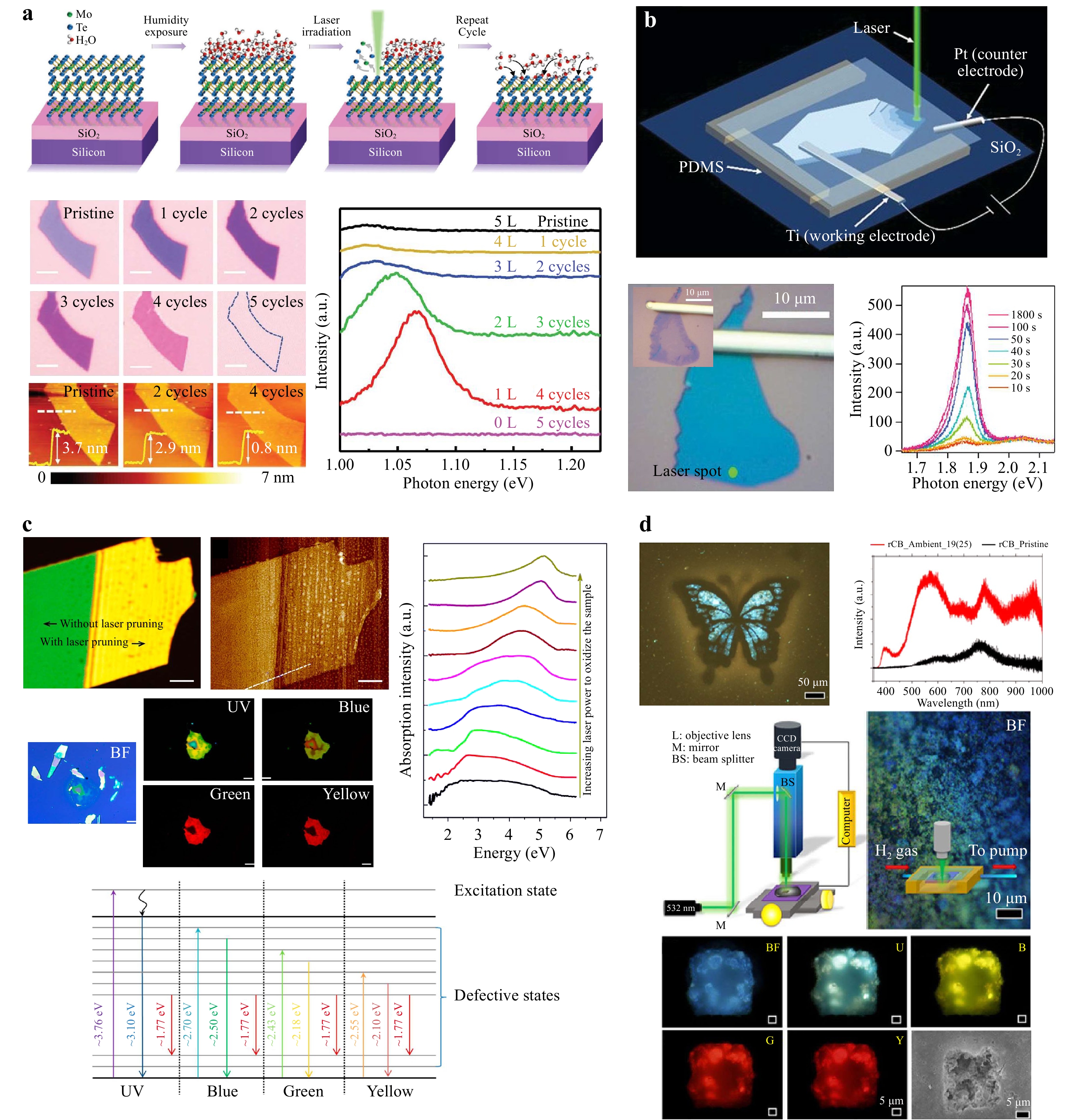
Fig. 3 Laser thinning and defect creation for nanomaterial fluorescence. a Accurate layer-by-layer thinning of MoTe2 under a humid environment with ultralow laser power. Reproduced with permission from ref. 82 Copyright 2018 Wiley-VCH. b Laser-assisted electrochemical etching of multilayer MoS2 with self-limiting mechanism down to monolayer level. Reproduced with permission from ref. 83 Copyright 2016 Royal Society of Chemistry. c Combinative interplay of laser thinning and oxidation for spatially selective activation of suboxide fluorescence on black phosphorus through bandgap engineering. Reproduced with permission from ref. 87 Copyright 2015 American Chemical Society. d Multicolored fluorescence patterning of common rCB via photothermal infusion of carbon into metal oxide impurities using a focused laser beam. Reproduced with permission from ref. 88 Copyright 2019 Springer.
With refined control over spatial manipulation of the focused laser beam, Venkatakrishnan et al. first demonstrated fluorescence patterning and writing through spatial selective thinning of WS2 multilayers, before further analyzing the effects of the focused laser irradiation on the acquired fluorescence86. Across a range of laser intensities, the monolayer fluorescence can be further modified for low-power oxygen-mediated enhancement or high-power quenching on a localized scale without discernible alterations in optical morphology, providing structured modifications for steganography transmission in ultrathin materials. This marks the first instance in the realization of information encryption within a material of atomic thickness. By evaluating the concurrent effects of laser thinning and oxidation during the lasering process, Lu et al. concluded the combined interplay of both processes in crafting few-layer phosphorene suboxides from thicker black phosphorus flakes (Fig. 3c)87. The overall band engineering from layer reduction and oxygen incorporation resulted in a nanomaterial with a wider bandgap and a broad range of PL owing to the various defect states present. With localized control and gas-sensitive changes to the effected PL, the modified nanomaterial is utilized in the domain of micropatterning and toxic gas sensing.
Analogous to the aforementioned instance of phosphorene suboxides, the initiation of broad-range fluorescence arising from defects or impurity color centers embedded during the laser procedure remains a common observation in the field. Particularly in nanomaterials with moderately wide bandgaps, the laser process can generate anti-bunched photons for single-photon quantum emitters. In sequence, some studies involving laser-generated defect-based fluorescence are briefly covered, before insights into specific quantum emitters produced through the laser influence on wide-bandgap hosts.
In recovered carbon black (rCB), Lim et al. utilized laser impact to infuse the carbon material into the minuscule amounts of ZnO impurities, functionalizing the economical by-product with multicolor fluorescence (Fig. 3d)88. Together with the presence of S impurities and lasered periodic arrangements of carbon nanoparticles, the confounding contributions provided multicolor emissions within the nanomaterial with ease of material transfer and voltage-controlled fluorescence on-off, leading to flexible optoelectronics in the context of sustainable material consumption. In contrast, the works by Castelletto et al., Buividas et al., and Saleem et al. adopted an alternate approach of generating luminescent point defects or vacancies through ultrafast femtosecond laser "knock-outs" within the respective wide-bandgap fused silica89, 90, hexagonal silicon carbide (SiC)91, cubic boron nitride (c-BN)92 and gallium nitride (GaN) crystals93. With GaN crystals in various forms (thin film, MBE-grown nanowires, Mg-doped nanowires), Saleem et al. reproduced the associated defect-compelled red luminescence in the nanocrystals, ranging from 620 nm to 680 nm in the production of nano-crater light sources within the materials. Similarly, c-BN exposure to ultrafast irradiation afforded broadband PL centered across the red spectral range, arising from the combined contributions of three Frenkel color defects owing to N-vacancy formation. With 4H- and 6H-SiC, high-power laser irradiation at 1030 nm efficiently propels the formation of sub-micrometer cavities with broad PL spanning the red and NIR regions, of which the NIR luminescence was decisively assigned to silicon-vacancy color center emission. Under strong UV laser irradiation, Zhou et al. and Zhang et al. independently observed varying PL peak distributions in fused silica accountable by the formation of oxygen-deficient centers and non-bridging oxygen hole centers, all of which stem essentially from the laser-driven loss of oxygen content and in place, the existence of dangling bond defect sites.
The advent of single-photon emitters (SPE) in wide-bandgap semiconductors has been regarded as a promising platform for quantum photonic readouts. More importantly, this uprise presents new light to laser technologies as a spatially precise option to create deep-level defects as quantum emitters with reduced damage to the surrounding host lattice. Across similar sets of dielectrics, the works of Hou et al., Chen et al., and Castelletto et al. have all presented sites of coherent, anti-bunched emissions with limited defect diffusion across the geographical 3D distribution. With diamond crystals lightly doped with nitrogen atoms, Chen et al. began with the creation of single nitrogen-vacancy (NV-) emission centers at a 45 ± 15% probability ratio in a correlated mix with double and triple NV- sites (Fig. 4a)94, before a subsequent improvement to near-unity exclusiveness of the single NV- variant95. In both works, the high accuracy and resolution in the positional ordering of the defect emitters reassured the capability of the acquired color centers to be stable prerequisites for various quantum technologies. In SiC and GaN, Castelletto et al. optimized the parameter controls across the laser wavelength, laser intensity, and doping extents in the insulator materials to modulate the extent of ablation damage, emitter density, and emission wavelength, respectively (Fig. 4b)96. With power-law dependence in the number of localized color centers produced, photoinduced ionization was deduced as the mechanism responsible for producing these quantum emitters within confocal diffraction limits.
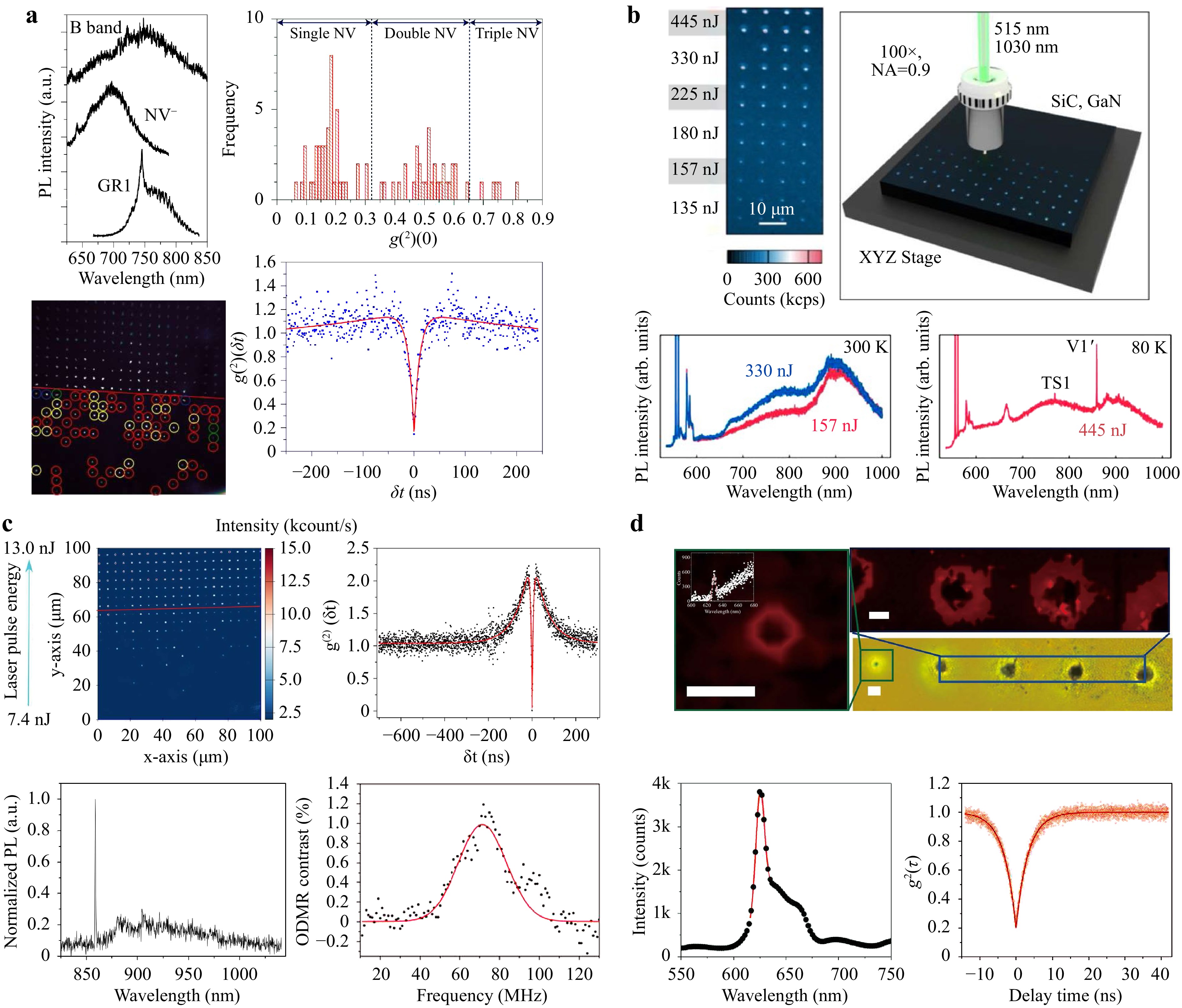
Fig. 4 Laser-created localized defects for single quantum emitters. a Laser writing of negatively charged nitrogen-vacancy point defects for fluorescent color centers in diamond crystals with minimal defect diffusion and high single defect percentage. Reproduced with permission from ref. 94 Copyright 2017 Nature Publishing Group. b Laser creation of color center array in silicon carbide using 515 nm femtosecond laser pulses of varying energy ranges. Reproduced with permission from ref. 96 Copyright 2021 Multidisciplinary Digital Publishing Institute (MDPI). c Laser-created silicon-vacancy in silicon carbide (4H-SiC) as single-photon emitters at 30% yield. Reproduced with permission from ref. 97 Copyright 2019 American Chemical Society. d Bright single-photon emissions in hexagonal boron nitride (h-BN) flakes through laser irradiated defects. Reproduced with permission from ref. 98 Copyright 2018 IOP Publishing Ltd.
In a related study, Chen et al. refined the laser irradiation process on 4H-SiC to generate single silicon-vacancy sites harbouring a 30% yield in stable emission centers within the ensemble array of individual quantum emitters (Fig. 4c)97. The sharp V1' quantum emissions were further characterized with g(2)(0) of 0.040 ± 0.003 and quantified of 16 photon involvement in creating a single defect color center. Working with h-BN in variants of monolayer crystals and commercial nanoflakes, Hou et al. concluded superior single-photon performance in laser-irradiated flakes designated by bright narrowband emissions with a line width of 1.4 nm and g(2)(0) as low as 0.20 (Fig. 4d)98. With relatively greater absorbance of the accorded laser exposure, the emitting craters within h-BN flakes allow ease of production at lower fluences with reduced substrate damage, illustrating greater prospects for quality nanosized emitters in quantum computing and photonic applications.
-
Alongside the capability of focused and ultrafast laser techniques to trigger material fluorescence through various means, the application of lasers towards refined modifications in the materials' innate emission remains undeniably important as well. By revising the peak wavelengths, intensities, and relative emission ratios from the various emissive states, laser modifications to the fluorescence profile of a material mark another handle imperative to the enhanced functionalization of nanomaterial properties. Using pre-synthesized CdSxSe1-x nanowires comprising the ternary alloyed composition, Lu et al. presented continual redshifts in the emission profile with an increasing degree of laser-prompted substitution in the sulfur content with ambient oxygen (Fig. 5a)99. The bandgap engineering process was corroborated by similar observations under thermal annealing in an oxygen environment. Furthermore, with the sample lasered under inert helium conditions, an alternate mode of spectral transformation was achieved by including additional broadband features stemming from defect-state emissions. Under such operations, progressive color changes can be managed with a single laser run to yield micropatterns with multicolor gradients. Exploiting the possibility of such laser modifications to the CdSxSe1-x variant, a subsequent study by Lu et al. involved CdSSe as a shell component to form hybrid ZnO/CdSSe core-shell nanowires100. With the formation of a type-II heterojunction interface, the subsequent laser-assisted oxidation of the CdSSe shell evolved color changes, incorporating a complex interplay between disparate factors ranging from defects to compositional and morphological alterations. Using a lower laser power threshold to induce fluorescence variations, the relatively less distinct optical contrast presents opportunities for micro-steganographic applications.
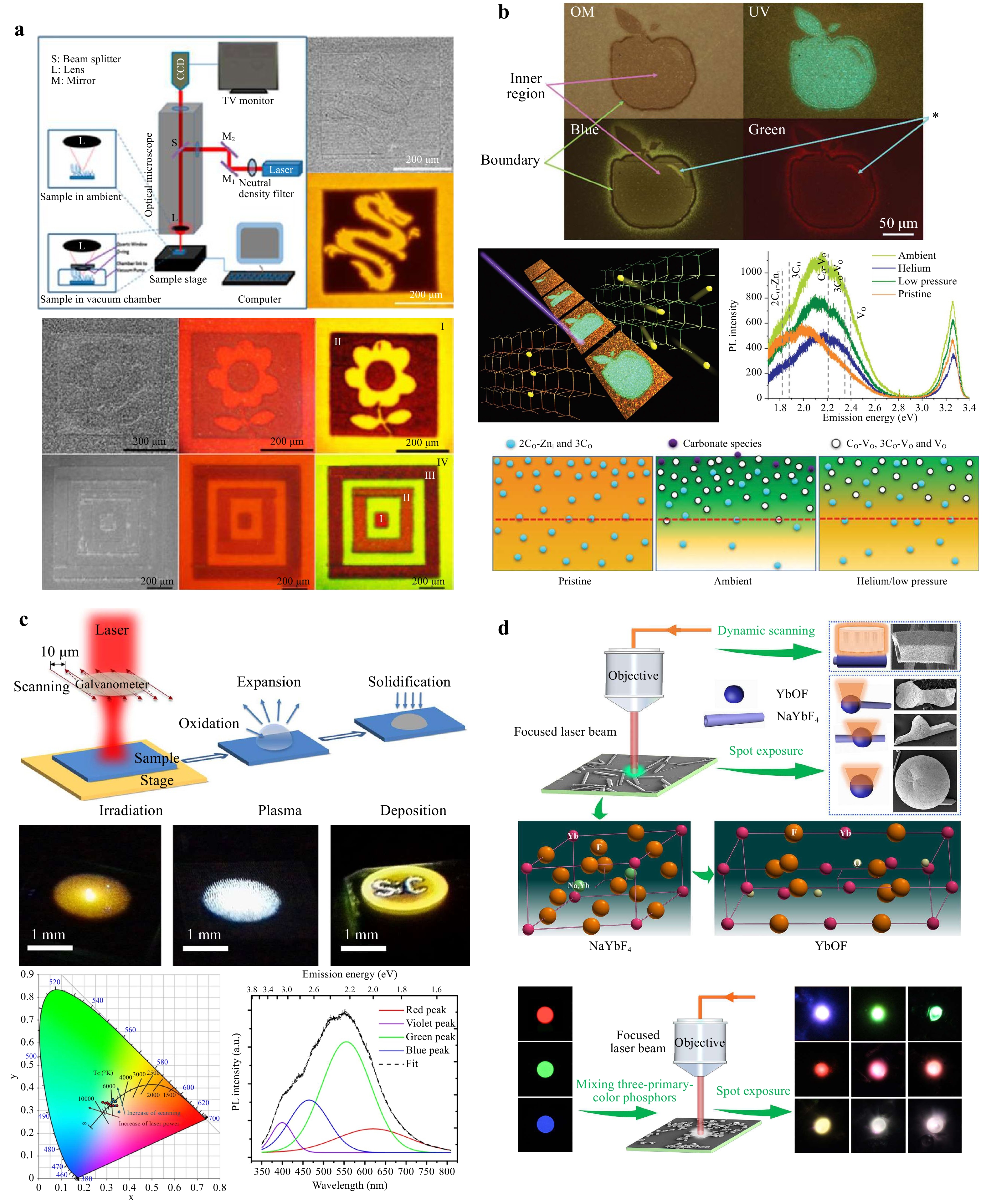
Fig. 5 Laser modification of fluorescence emission profiles in nanomaterial structures. a Laser-adjusted emission redshift in pre-formed ternary alloyed CdSxSe1-x with laser-inflicted oxidation. Reproduced with permission from ref. 99 Copyright 2012 American Chemical Society. b Laser-induced emission blue shift with color variation in carbon-doped zinc oxide (C-ZnO) nanowires owing to laser annealing and oxidation. Reproduced with permission from ref. 101 Copyright 2019 Royal Society of Chemistry. c Laser-modified fluorescence in SiC with controllable white emission color temperature arising from the formation of silicon oxycarbide species. Reproduced with permission from ref. 105 Copyright 2018 Nature Publishing Group. d Laser welding of lanthanide-doped nanostructures to heterojunctions and mixed color fluorescence heterostructures. Reproduced with permission from ref. 109 Copyright 2021 Wiley-VCH.
Beginning with C-doped ZnO nanowires, Chua et al. investigated the ability of the laser beam to recalibrate the population of emitting defect combinations within the nanowire host (Fig. 5b)101. From dominant orange emissions originating from 2CO-Zni and 3CO defects abundant in the pristine nanowires, a subsequent evolution to an intense green fluorescence, comprising CO-VO, 3CO-VO, and VO-based emissions, became distinct with increasing oxygen content during the laser modification process. The mechanistic model involving carbon migration and ZnCO3 formation was evidenced by computational methods, X-ray photoelectron spectroscopy (XPS) surface analyses, and plasma etching processes. These processes validate the origins of the observed conversion in fluorescence while unraveling insights into the volatile defect chemistry embedded within C-doped ZnO nanowires.
In comparison, Shimogaki et al. subjected ZnO nanorods to P+ ion implantation and laser annealing, revealing the optical variability of these nanorods in relation to the defect density at each of these processing steps102. The intense implantation procedure was found to ingrain the crystal lattice with an abundance of defects, robbing the system of its near-band-edge (NBE) UV and oxygen vacancy (VO)-based visible emissions. The respective VO or NBE assigned emissions were selectively recovered upon post-annealing treatments with either thermal or laser processes. Consequently, the superiority of laser treatment in the recrystallization of top-quality p-type (P+-doped) ZnO nanorods was exemplified in the convenient creation of ZnO p-n homojunctions through localized laser exposure.
Operations assisted by laser source irradiation on wide-bandgap materials have also influenced fluorescence chromaticity and intensity by dint of controlled oxidative metamorphosis and interfacial interactions. Variations in the oxygen content available during PLD of Si nanocrystals were evaluated by Chen et al., of its effects on the activated nanomaterial photoluminescence103. In particular, a holistic investigation concluded multifaceted contributions from emitting interfacial states and quantum confinement effects in a complex polycrystalline-Si@crystalline-SiO2@amorphous-SiO2 nanostructure. Meanwhile, laser-initiated post-oxidation of mesoporous Si nanowires (mp-SiNWs) and SiC wafers were separately reported by Choi et al. and Wang et al., regulating the respective emission wavelengths and color attributes. The optical contrast (under UV excitation) from laser patterning of the oxidation-etched nanowires was strongly discernible, exuding a fresh burst of striking greenish-blue hue amid the original reddish emission background104. Scrutinized under various characterizations and laser-cut conditions, the onset in the fluorescence changes was explained by Si/SiO2 interfacial states and oxygen defects created in varying abundance with the evolving stoichiometry in Si:O across different durations of laser exposure. Using similar mechanistic processes, Wang et al. oxidized SiC to SiOC, generating white emissions with tunable color temperatures through a combination of inputs from a multitude of defect types (Fig. 5c)105. The concomitant doping effect encouraged the fabrication of p-n junctions to an eventual white light-emitting diode (LED).
Moreover, recent instances of laser-induced oxidation and recrystallization in insulator hosts with complex chemical compositions have demonstrated efficient optical modulations. For example, different extents of laser perturbation inflicted upon the insulator host NaYF4 – the workhorse material in rare-earth upconversion technologies, have also bestowed fine-tuning capabilities in the dopant emission profiles. Assisted by hot carriers from plasmonic nanoparticles, the enhanced thermal and catalytic inputs to complete oxidation of NaYF4 to Y2O3 nanocrystals at low laser powers were realized by Zhang et al.106 With careful selection of appropriate excitation wavelengths to drive the corresponding plasmon resonance, polycrystalline fluorides were instantly transformed into Y2O3 with significantly improved crystallinity. This bypasses the YxOyFz intermediates to yield a restructured spectral distribution with greater intensity and monochromaticity.
In an identical representation, Kong et al. revisited the plasmon-aided transformation, replacing Au nanoparticles with pre-evaporated Au/Ag nanoislands to exclude random adsorption or encapsulation of any metallic residual as contamination to the transformed nanocrystal products107. Analogous spectral remodeling was achieved, yet comprehensively explored across a greater multitude of parameters, including laser power, wavelength, nanoisland size, and inter-island gap, in dictating the efficiency of the oxidative conversion. Without any plasmonic reinforcement, Gao et al. reported partial oxidation instead, at the surface of NaYbF4 nanocrystals to afford NaYbF4@YbOF heterojunction from an intra-crystal perspective. The spatial concentration of laser irradiation atop a single end of the NaYbF4 nanowire influenced the upconversion intensities and colors at both ends of the nanowire108. By influencing the dynamic light-light and light-heat interactions with the nanostructure, the associated oxidative changes readjusted the spectral weightage emanating from different optical transition states within the Ho3+ dopant. Subsequently named the laser irradiation welding approach (LIWA), Gao et al. further applied this technique to expand the upconverted color palette (Fig. 5d)109. By welding nanoparticles comprising three primary colors into a single entity, mediation by the YbOF interface resulted in multicolor tuning owing to the correlated mix of individual color contributions. Furthermore, with the presence of the YbOF component as a mismatched heterojunction at the NaYbF4:YbOF juncture, the contrasting lattice phonon energy supported non-radiative quenching of higher energy transitions, redistributing the intensity contributions from the diverse transition peaks to derive the alternate mode of color modification.
The application of laser systems in spatially precise recrystallization of rhombic LuF3:Yb3+, Er3+ nanoflakes was recently reported by Min et al., who demonstrated a photothermal reaction at the Yb3+ sensitizer to drive an amorphous-to-crystalline reconstruction at the peripheral lattice of the nanocrystal110. The process of "atomic level passivation" strengthened the luminescence by 484-folds, resolving the persistently weaker emission immanent in UCNPs. In contrast, Dong et al. used nanosecond-pulsed lasers to offer a non-trivial role in adjusting the optical properties of CsPbBr3 perovskite crystals through a synergy of nanostructure reshaping and improvement in crystallinity111. The differing degrees of quantum confinement and bandgap engineering, along with narrowed polydispersity and lattice reorganization, yielded optimal crystals of reduced Urbach energies with quality fluorescence of varying wavelengths.
In association with the ultrathin nature and optical sensitivity of 2D TMDs, the influence of lasers extends monumental impact upon the material fluorescence from the perspective of defect chemistry and exciton photophysics. Leveraging the sensitivity of 2D material surfaces to the surrounding environment, Lu et al. exploited a focused laser beam to atomically heal WSe2 and WS2 monolayers, passivating surface chalcogenide vacancies with oxygen atoms for fluorescence control79, 86. Zhao et al. translated the dynamic relation between 2D material fluorescence and surface oxygen species into a direct write-in, visual read-out data storage platform using a WS2 monolayer. The rewritable data encryption system depended on the interplay between the fluorescence-suppressing adsorbed O2 species and the laser healing–defect engineering process to modulate the optical patterning of the monolayer surface. The information can be flexibly erased by ozone treatment and re-written by the focused laser beam, exhibiting an ingenious design for the thinnest rewritable compact disk (CD-RW), and propelling optical data storage technologies towards atomic scales112. Using a reactive H2S gaseous precursor, Afaneh et al. performed localized photoconversion of a WSe2 monolayer via spatial substitution of selenium components with sulfur atoms (Fig. 6a)113. With varying degrees of substitution and dopant distribution, the work accounts for the formation of either a doped TMD or heterostructure morphology, with graduated PL ratios while preserving the initial high crystallinity of the monolayer. Comparatively, Kim et al. demonstrated the unconventional p-type doping of a plethora of TMDs with phosphorus atoms, starting with a similarly reactive PH3 gaseous reactant under the laser114. The spatial and quantitative precision of the laser doping process provided stable adjustments in the PL intensities of the respective TMDs depending on their inherent p- and n-type natures.
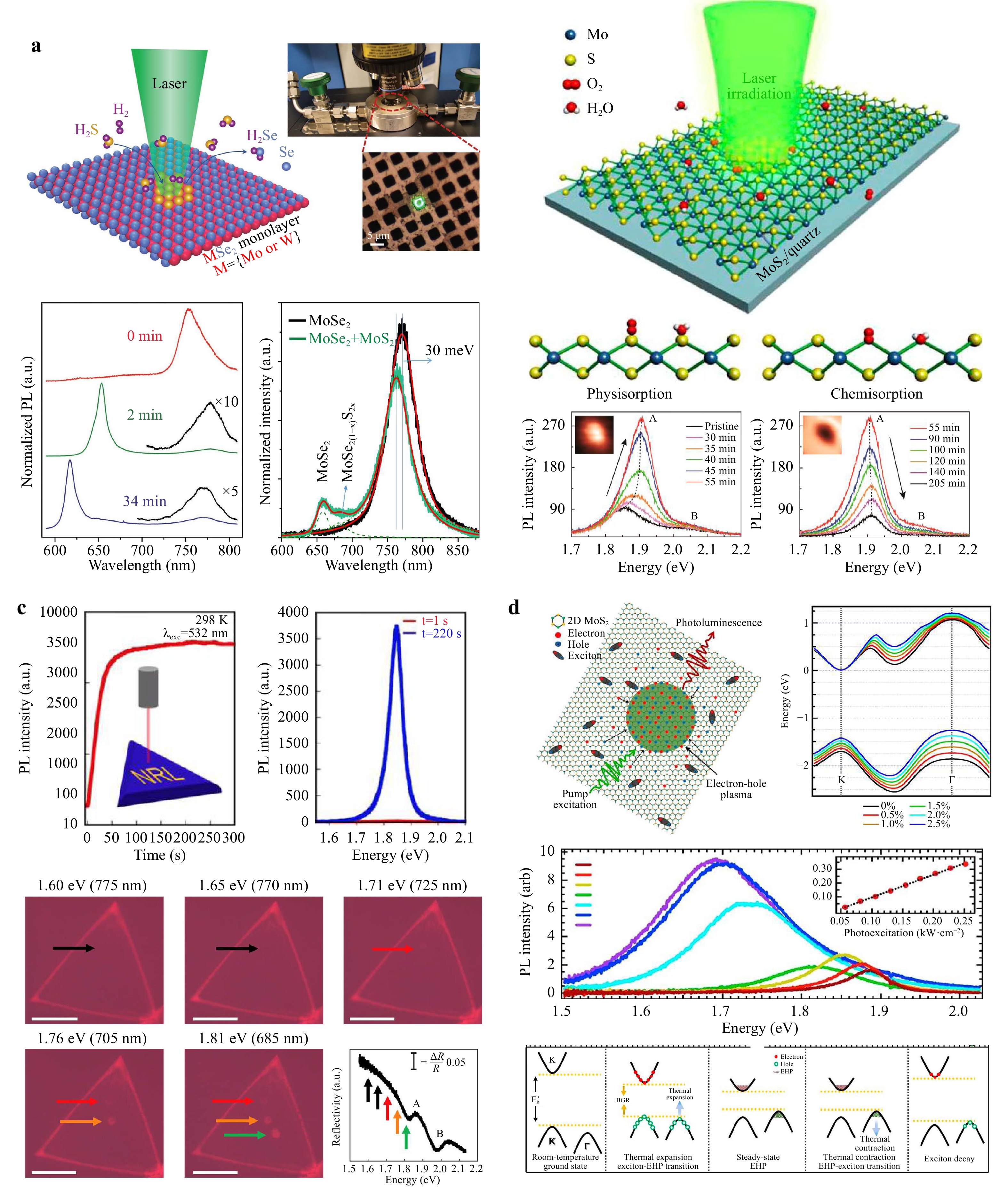
Fig. 6 Laser modification of fluorescence emission profiles in 2D TMDs. a Laser-assisted chalcogenide substitution in Mo and W-based TMDs for concentration-dependent tuning of spectral features. Reproduced with permission from ref. 113 Copyright 2018 Wiley-VCH. b Mechanism investigation of PL and chemical changes in monolayer MoS2 in correlation with laser irradiation duration. Reproduced with permission from ref. 118 Copyright 2016 American Chemical Society. c Wavelength dependent laser effected PL enhancement in monolayer MoS2 due to suppressed non-radiative processes with adsorption-desorption dynamics. Reproduced with permission from ref. 119 Copyright 2019 American Chemical Society. d Investigation of strong broadband emission from dense electron-hole plasma produced from the photothermal restructuring of band structure and crystal lattice in Mo-based dichalcogenides. Reproduced with permission from ref. 120 Copyright 2019 American Chemical Society.
Beyond the deliberate inclusion of variable dopant sources (Se, PH3) into the laser modification process, optical transformations emerging from laser-affected interactions between monolayer TMDs and ambient molecules have also been examined extensively. The different molecules, videlicet oxygen and water, have been scrutinized for their diverse significance in the optical and electronic performances in TMDs. Specifically, the work of Bera et al. reported a multi-fold increment in the acquired signals from trion and exciton emissions, as well as longitudinal Raman modes, during ambient laser irradiation115. The mechanistic contributions from the cooperative effects of defect healing and p-doping were accurately substantiated across similar literature works116–117.
In a more elaborate study, Oh et al. examined ambient laser modification across extended irradiation durations, conclusively demarcating initial mild physisorption to subsequent chemisorption before an eventual degradative photoquenching (Fig. 6b)118. The corresponding PL trend from gradual increment to a sharper spike before the severe decline critically reflects the role of photo-oxidation extents in influencing the optical performance of the monolayer. Narrowing to specific ambient moieties, Sivaram et al. and Lee et al. independently ascribed impressive gains in monolayer TMD PLs to H2O and O2 influence, respectively, reasoned through distinctive mechanisms. With H2O, Sivaram et al. emphasized the importance of a wavelength-dependent exciton generation process as a prerequisite for the sequential passivation of sulfur vacancies by H2O molecules (Fig. 6c)119. The associated PL brightening was proposed to require sufficient photon energy to overcome the barrier for successful H2O passivation, yielding enhanced bound and neutral exciton intensities from reduced rates in non-radiative recombinations. Through favorable reduction of the non-radiative exciton-exciton annihilation (EEA) process, Lee et al. explained the intricacies involving oxygen adsorption over sulfur vacancy sites (Fig. 6d)120. Laser implantation of atmospheric oxygen is expected to hinder exciton diffusion, hampering EEA operations that typically limit monolayer PL at nominal photoelectron densities owing to non-radiative de-excitation between excitons in close proximity.
Alongside the surface passivation procedures, the presence of vacancy sites marks yet another criterion for the realization of PL enhancement. Examining aged monolayer samples, Ardekani et al. and He et al. revealed the propensity of laser irradiation to liberate surface adsorbates in the reinvigoration of defective surface properties. Under cryogenic conditions, the spectroscopic changes captured by He et al. could be effectively toggled between states of multitude excitonic emissions and lone defect-bound emission, simply from a reversible cycle of laser treatment and thermal annealing121. Post absorbate removal, Ardekani et al. proceeded with laser-modulated oxygen absorption-desorption on the monolayer surface through vacuum-oxygen cycles and femtosecond laser pulse exposures122. The former environmental control alters the spectral features, whereas the latter presents temporal, instantaneous spectral changes upon laser on-off, all within the basis of trion suppression and exciton enhancement from oxygen p-doping.
By leveraging the exclusiveness of monolayer fluorescence, Lee et al. and Mannebach et al. independently exploited the optical compressive forces emanating from the laser source to calibrate the interlayer distance, effectively tuning the extent of interlayer coupling and fluorescence between exfoliated WSe2 and WS2 monolayers123–124. Regional quenching in the laser-irradiated domains reconciled with the progressive transformation from a non-coupling interaction into a strongly coupled regime, pinpointing the elusive onset of interlayer coupling with potential for band engineering and micropatterning features. Kang et al. instead induced the renowned 2H to 1T phase transition in MoS2 monolayers, liberating PL shifts in accordance with the incident excitation wavelength125. The interplay between laser excitation and the resonant plasmon modes in the Au NP laced atop the monolayer prompted hot electron generation to encourage reversible phase reconstruction.
Complementary to intentional laser modification experiments, a handful of notable studies have also assessed, as a precautionary measure, related effects inadvertently evoked by the excitation laser source of the PL instrumentation. The onus on these works lies in clarifying unwanted in situ modifications that may exist during data acquisition, which is imperative to evaluate and eradicate in assurance of accuracy from the resultant PL spectra.
Using low laser fluences on the order of tens to hundreds of microwatts conventional to standard PL measurements, Cadiz et al. and Currie et al. reported revisions to excitonic ratios under such measurement conditions in vacuum. Specifically, they independently evaluated the respective MoSe2 and WS2 monolayers of improved excitonic PL, with the trions eventually surpassing neutral exciton contributions in overall intensity. The reversibility of the peak ratio redistribution upon exposure to ambient conditions reiterated the importance of the measurement environment on the resultant PL spectra. In addition, Cadiz et al. assessed MoS2 samples under identical conditions, yielding a vanishing exciton PL and spectral redshift from an alternate mechanism126, whereas Currie et al. added a thorough manipulation of exciton conversion to achieve states of purely trionic inputs, described with the associated Raman evolutions127.
Meanwhile, Yu et al. elucidated the consequences of the EEA mechanism in TMD monolayers across a broad range of laser power densities128. Dominant at high excitation intensities, the process prompted excitonic decay with saturated luminescence efficiency beyond 1010 cm-2 exciton density, marking a critical consideration for PL evolution studies, especially in the strong irradiation regime. Furthermore, the study evaluated substrate influences, concluding a diminished EEA magnitude for monolayers supported on a silicon substrate. These results further highlight the importance of substrate selection under these measurement conditions.
In contrast, the analysis by Bataller et al. unravelled a transition from excitonic states to stable electron-hole plasma/liquid (EHP/EHL) phases upon photoexcitation above a critical irradiation density129. Despite a direct-to-indirect bandgap transition due to photothermal expansion in the free-standing monolayer, the simultaneous EHP construction was characterized by sudden spikes in PL intensity, along with extended carrier lifetime pertaining to the broadband peak profile. It was ascertained that while the EHP mainly comprises indirect band mechanics, new carriers in the direct band generated by the continuous photoexcitation were found to recombine at impressive efficiencies. This phenomenon occurs along with suppressed Auger processes in the degenerate plasma, leading to seemingly contradictory upheaval in both carrier density and lifetime.
-
In this subsection, an alternate mode of laser operation is briefly discussed: laser-directed patterning of originally fluorescent materials. Although not directly contributing to the material chemistry or photophysics of nanomaterial fluorescence, nonetheless, this section involves the relevance of laser systems to dictate fluorescence distribution for micropatterning and related applications.
For instance, by laser engraving morphological patterns on a dense MWNT array, Lim et al. first demonstrated the preferential deposition of CdSe/ZnS QDs conforming to regions of the micropatterned contour at higher altitudes (Fig. 7a)130. Further evaluation of the nanoparticle diffusion dynamics revealed that the interconnected nanotube meshes effectively sieved the QDs with precise size differences down to 0.5 nm. With differential size-dependent fluorescence of the QDs resulting from quantum confinement, the filtered dispersion translates into an emission color gradient of the QDs along the depth of the nanostructure. This adds a layer of patterning tunability in the z-axis, resulting in 3D multicolored functional hybrid patterns crafted by laser pruning.
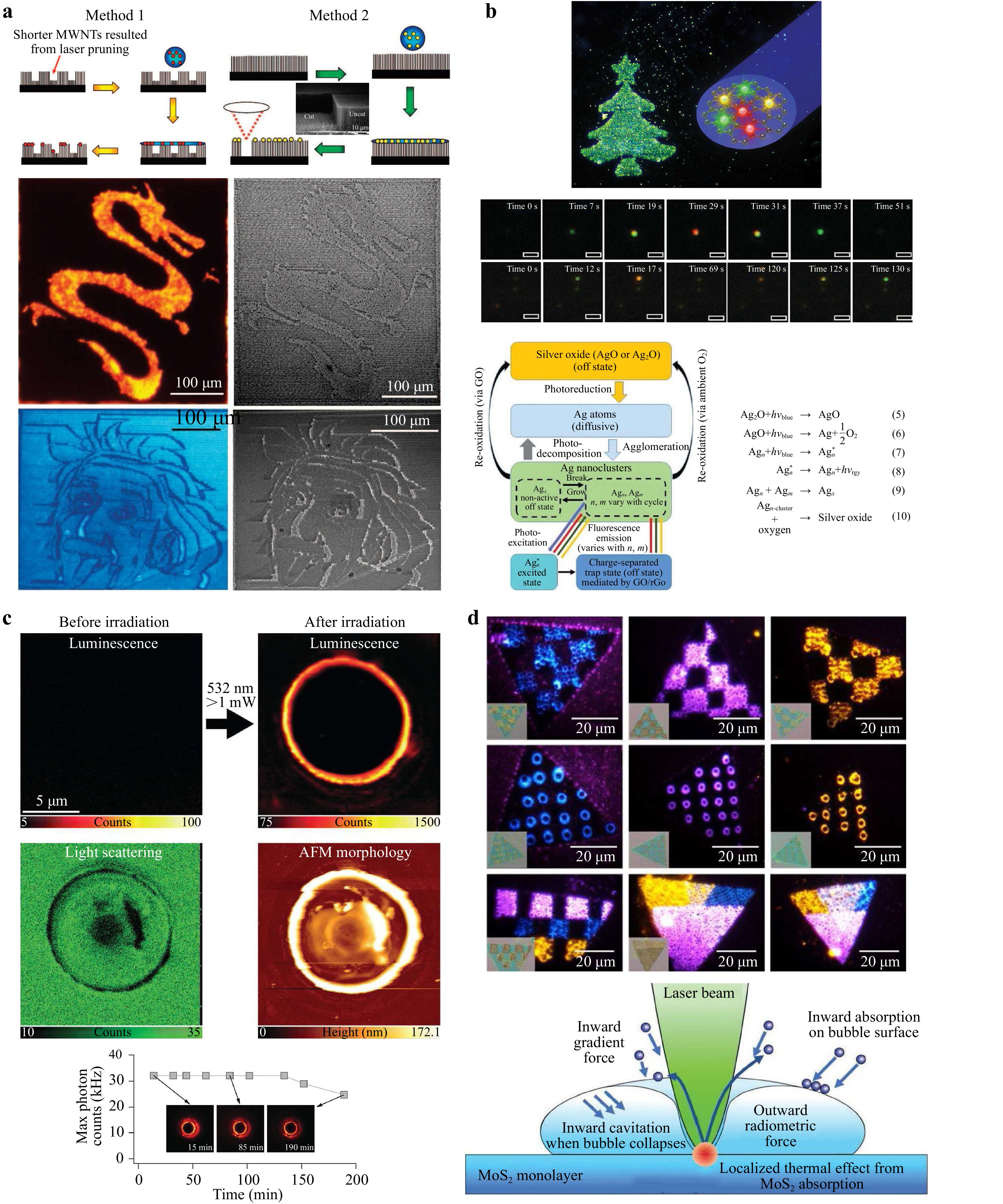
Fig. 7 Laser-assisted patterning of fluorescent nanomaterials. a Laser micromachining of carbon nanotube array for the depth-dependent size distribution of fluorescent CdSe/ZnS quantum dots (QDs) with depth-correlated emission color in the laser pruned patterns. Reproduced with permission from ref. 130 Copyright 2008 American Chemical Society. b Laser-driven formation of Ag NPs in a patterned distribution over GO film as nanoblinkers with dynamic fluorescence color change from redox cycling between Ag ionic states. Reproduced with permission from ref. 131 Copyright 2018 Royal Society of Chemistry. c Formation of bright luminescent organic micro-rings under laser optical influences. Reproduced with permission from ref. 136 Copyright 2017 Royal Society of Chemistry. d Laser-supported microbubble formation for dynamic in solution UCNP assembly for patterned nano-arrays with composite upconversion colors. Reproduced with permission from ref. 137 Copyright 2019 Wiley-VCH.
In a bid for greater patterning complexity, Lim et al. also offered a dynamic color-changing micropattern constructed from Ag NPs emplaced on an underlying GO substrate (Fig. 7b)131. Post-laser-assisted positioning of the Au NPs, continuous blue light irradiation allowed for ceaseless tricolor intermittent nano-blinking owing to active oscillatory chemical redox at the nanoparticle sites, endowing a transferrable micropattern with light-sustained color cycling features sensitive to molecular analytes.
In addition to the in situ patterning of fluorescent nanostructures by the input of photonic energies and nanoparticle self-assembly post-laser pruning, optical forces from laser irradiation also contributed to the hallmark influence in coordinating the positioning of nanomaterials through gradient and radiometric forces. Compared to traditional optical tweezer implications on micro-sized particles and aggregates132–134, Poh et al. and Kwon et al. respectively assembled UCNPs and Rhodamine 6G (R6G) dye molecules of smaller dimensions into ring-like aggregation features with the assistance of the incident laser. The conformation of such microstructures likely emerged from the interplay between optical forces and surface energetics at a microbubble-solvent interface, as evaluated in similar studies135. The combination of strong light absorbance and microbubble formation at the deposition site bestowed Kwon et al. with the production of bright, photostable micro-rings with relative ease of operation (Fig. 7c)136, whereas Poh et al. designed various multicolor micro-canvases with superb adhesion of the emitting UCNPs above atomically flat MoS2 substrates (Fig. 7d)137.
-
The scope of the discussion is confined to laser systems, specifically towards the activation, modification, and spatial designation of material fluorescence. The summary spans a plethora of materials, ranging from hybrids involving metallic nanoparticles, carbon dots, 2D TMD ultrathin films, wide-bandgap nanomaterials, and upconversion nanocrystals. In the context of laser-induced fluorescence, the initiation of nanomaterial emission can be attained simultaneously with ingenious styles of nanomaterial formation and defect generation through the indirect effects of laser irradiation. Such in situ alterations allow the production of nanomaterials with desirable optical traits. Particularly towards 2D TMD films, the process of laser thinning down to the monolayer limit, denoted by the emergence of its peculiar fluorescence property, also amplifies the capability of laser systems to controllably probe the unique optical functionality for further studies on its excitonic physics.
In comparison, the subsection dedicated to laser-modified fluorescence focused on the domain of spectroscopic changes in correlation with varying extents of laser exposure. With the energetic input of the incoming photons, the nanomaterials can overcome activation barriers pertaining to redox and recrystallization processes to realize modulated PL spectral profiles. Concomitantly, unintended spectroscopic changes arising from laser excitation of optical characterization techniques, especially applicable to sensitive ultrathin 2D materials, were also emphasized with the intention of awareness and avoidance of such concealed sources of measurement inconsistency. Nonetheless, the manipulated modifications in fluorescence intensity, lifetime, color, peak full-width-half-maximum (FHWM), and weighted peak ratios supported an advanced understanding of the mechanics of the fluorescence emissions, in conjunction with the relative ease and reproducibility of attaining these states under refined tunability. Finally, the review marks off with a short section on laser-assisted patterning, in which the laser-bestowed spatial precision prompted the formation of functional nanohybrids for microscale patterning.
Although such explorations have been summarized in brevity throughout this review, lasers are expected to still hold significant potential in the realm of laser-induced fluorescence in nanomaterials. Over the past century, the provision of luminescent materials has provided unprecedented opportunities in the domains of biological and chemical fluorometric sensing, as well as biological imaging functions. Such technologies have heightened material capabilities in attaining detection sensitivities down to picomolar concentrations and single unit mismatches, along with in situ dynamic monitoring of biological systems. The contributions of lasers linger within the ease of flexibility, low cost, and high-throughput production of these functional nanostructures with compositional control. The instances of multicomponent laser ablation systems, laser-driven multicomponent patterning, and laser-induced nanostructure welding presented the convenience of designing nanocomposites with mixed components and multicolor characteristics. Generally, these imbued properties expanded the family of permissible fluorescent entities with color tuning across the entire color gamut and emission efficiencies, providing sensitive and accurate detection platforms. The long-standing utilization of lasers to carve morphological patterns along material surfaces, together with localized surface reactions that produce surface inhomogeneity, have provided a means for 2D/3D nano-sculptures and optically contrasting patterns. With micro-machining and micro-sculpting processes offering complex multi-dimensional microstructures, the complementary modus operandi of laser patterning contributed towards steganographic and micro-encryption technologies, supported by decoding platforms using optical contrast and discrete differences in emission wavelengths and lifetimes. The role of lasers is discerningly significant. Through irradiation-induced thermal and chemical processes on the material surface, the repercussions on multiple material properties proliferated the modes available for encryption readout.
Looking forward, there remain numerous unexplored potentials in laser techniques for sensing and patterning platforms with greater complexity. For instance, representative works marking the flexible integration of disparate nanomaterial components into heterojunctions or single entities with compositional control could indicate the onset of multiplexed and multimodal platforms for these various applications. Through laser-assisted merger or fabrication of nanostructures that incorporate nano-units with dissimilar excitation-emission profiles, emission lifetimes, or absorbance, the reduced crosstalk between these components can evoke multimodal operation of a single nanostructure variant, controllable under different perturbation conditions. For example, the merging of a UV-excitable nano-component with a NIR responsive counterpart can easily provide individual nanocomposites or patterns that can selectively unravel the corresponding fluorescence emissions under differentiated excitation wavelengths or sensing conditions. Similarly, with spatial control and segmented growth capabilities of the respective nanopatterns and nanostructures through laser localization, the formation of multicolor fluorescence structures would also cater to an extensive database of color permutations applicable for multiplexed detection and sensing. By positioning and welding nanostructures of different emission colors in adjacent segments, customizable multicolor barcodes may be created in limitless combinations via the lasering process. Furthermore, we envision the association of lasers with defect-based single-photon emission and modification of 2D materials to hold significant prospects, particularly with a trending focus on boundless potentiality in quantum computing. While the manipulation of SPEs and photon correlation may provide a basis for laser-driven photon entanglement, controllable laser engineering of excitons and valley spins in 2D materials may hasten the development of qubits, all with tremendous contribution in the near future development of quantum technologies.
Furthermore, the exploitation of lasers for localized material modification is expected to contribute to investigations involving surface and interfacial states, notably for laser-crafted p-n junctions and metal-insulator-semiconductor (MIS) interfaces straddled across both lateral and vertical geometries. The chemical and physical modification of nanomaterial sub-domains may afford hetero- and homojunctions for the evaluation of work function modulations, as well as charge and thermal transport functions. With the multimodal proficiency of the laser, active material domains with variable chemical nature can be flexibly segregated and reshaped to conform to novel device geometries. The combination of laser pruning and laser modification is expected to afford customizable material cross-sections fitting to any intended unique device and interconnect geometries, spawning new avenues for multidisciplinary explorations spanning optical and electronic fields. With the laser system as an invaluable tool for refined material engineering, the flexibility of material design is anticipated to accelerate the pace of materials research.
Multifaceted Approaches to Engineer Fluorescence in Nanomaterials via a Focused Laser Beam
- Light: Advanced Manufacturing 3, Article number: (2022)
- Received: 28 July 2021
- Revised: 10 January 2022
- Accepted: 14 January 2022 Published online: 14 March 2022
doi: https://doi.org/10.37188/lam.2022.004
Abstract: Fluorescent nanomaterials have long been recognized as essential contributors to the advancement of material technologies. Over the years, the rapid expansion in this massive selection of materials has led to the emergence of systems with tunable and unique fluorescent properties, occupying pivotal roles across niche areas in imaging, photonics, micro-encryption, and steganographic applications. In recent years, research interest in the translation of laser-based operations towards the production and modulation of nanomaterial fluorescence has been reignited, owing to its ease of operation and low cost. In this paper, we summarize the assortment of laser operations for the fabrication, modification, and spatial positioning of various fluorescent nanomaterials, ranging from metallic nanoparticles, carbon dots, 2D ultrathin films to wide-bandgap nanomaterials, and upconversion nanocrystals. In addition, we evaluate the importance of laser-modified fluorescence for various applications and offer our perspective on the role of laser-based techniques in the forthcoming advancement of nanomaterials.
Research Summary
Nanomaterial Fluorescence: Laser activation, modification, and patterning
For decades, focused lasers have been useful in altering, redesigning, and reshaping nanomaterials for improved and novel properties. In particular, the role of lasers in modifying nanomaterial fluorescence provides enhanced optical functionality that caters to a broad range of applications. Led by Chorng Haur Sow from the National University of Singapore, a team of research scientists at the Nanomaterials Laboratory presented a review on the use of existing laser technologies at influencing nanomaterial fluorescence. Summarizing across a plethora of nanomaterials, they discussed instances of laser assistance in synthesizing and patterning fluorescence nanostructures, and modifying existing nanomaterial fluorescent profiles. This timely review is expected to summarize the existing technologies and prompt the next generation development of laser operations for advanced fluorescent nanomaterials.
Rights and permissions
Open Access This article is licensed under a Creative Commons Attribution 4.0 International License, which permits use, sharing, adaptation, distribution and reproduction in any medium or format, as long as you give appropriate credit to the original author(s) and the source, provide a link to the Creative Commons license, and indicate if changes were made. The images or other third party material in this article are included in the article′s Creative Commons license, unless indicated otherwise in a credit line to the material. If material is not included in the article′s Creative Commons license and your intended use is not permitted by statutory regulation or exceeds the permitted use, you will need to obtain permission directly from the copyright holder. To view a copy of this license, visit http://creativecommons.org/licenses/by/4.0/.

 DownLoad: