


-
Photonic integrated circuits (PICs), capable of transmitting light waves in prescribed waveguides with low cost, high speed, low power consumption, large bandwidth, and high integration1–3, are used in a wide range of applications, such as communications4,5, chip-scale optical signal processing6,7, and analog computing8,9, as well as in emerging fields like bio-sensing and quantum computing10–15. Large-scale functional PICs typically involve various optical devices, such as grating couplers, wavelength splitters, and mode converters16–18. As the dimensions of the waveguide devices’ input and output are usually not identical, high-efficiency connectors are required to interconnect them. Among them, the waveguide taper can interconnect different photonic devices by tapering the waveguide width19–21. However, to meet the coupling characteristics of the waveguide taper, it typically requires hundreds of microns in length to achieve high transmission efficiency and mode purity when the waveguide width-scaling ratio is large, which hinders the integration of PIC devices22,23. In addition, if the taper angle is too large to reduce the dimensions, this violates the coupling characteristics of the waveguide taper, resulting in the inability to achieve a collimated phase plane, which limits some on-chip applications. One of the most effective ways to improve the integration of PICs requires the reduction of both the on-chip photonic interconnector footprint and corresponding insertion loss as well as the maintenance of the collimated phase in waveguides with different widths.
Metasurfaces are recently attracting considerable attention in the field of photonic research, demonstrating unprecedented strength in manipulating the phase, amplitude, and polarization of incident electromagnetic waves24–29. By integrating PICs with metasurfaces, the performance and integration of the device is improved through flexible regulation of the optical response of guided waves at sub-wavelength scales, leading to unprecedented on-chip applications based on metasurfaces for mode conversion26,30,31, polarization rotation32,33, and wavefront shaping4,34. Metalens is a prominent device for on-chip optical focusing, which has been widely used for mathematical operation, beam steering, and mode-spot size conversion4, 21, 35, 36. In recent years, silicon-based optical waveguides have emerged as one of the most advanced and well-established photonic integration platforms, thanks to the advantages, such as low loss, compatibility with CMOS technology, and high integration density. They have been widely used in many applications, such as data communication37, sensing38,39, and optical signal processing40-42. Fan et al. reported the first integrated metalens consisting of plasmonic nanocubes loaded on a 220 nm-thick silicon-on-insulator (SOI) waveguide to shorten the taper’s length43. Furthermore, a 2D Bessel beam was demonstrated by creating an integrated nano-axicon. Subsequently, researchers used regularly shaped dielectric meta-atoms to form new types of on-chip metalenses to avoid ohmic losses. For example, Wang et al. implemented a metasurface by defining 1D rectangular etched slots in the waveguide4 and varying the slot length along the transmission direction to achieve the desired wavefront with low loss. The proposed on-chip metalens had a footprint of 10.5 × 2.5 μm2 at a transmission efficiency of 90%. Ren et al. demonstrated an on-chip light focusing device using rectangular etched slots on a waveguide with large all-dielectric metasurfaces21. Notably, a large width-scaling ratio usually implies that the metalens has a large numerical aperture (NA), that is, the phase gradient in the metasurface is relatively large. Local approximations based on periodic boundary conditions ignore the gradient coupling effect in the actual arrangement of meta-atoms, leading to a mismatch between the ideal and actual devices, which harms the mode purity of the final device.
Recently, with the rapid development of computational optimization capabilities and advances in micro/nanofabrication technologies, free-form integrated photonic devices using inverse design have shown spectacular progress in terms of integration and efficiency44–47. Inverse design can further minimize device dimensions with high performance. Promising results have been obtained from the on-chip integration of metasurfaces designed via adjoint topology optimization48–51. Sell et al. used the topology optimization method to produce a beam splitter with nonintuitive layout and demonstrated relative efficiencies of over 80% for both the TE- and TM-polarized light52. Yang et al. reported a chip-to-chip multimode link using an inverse designed coupler whose dimensions were limited to less than 10 μm and 3 dB bandwidth of over 35 nm for all the mode channels5.
In this study, we proposed an on-chip metalens, in which a free-form metasurface is embedded in the thin silicon film of an SOI substrate to achieve dual functionalities, that is, beam focusing and collimation, for different incident directions. The footprint of the proposed device is only 2.35 μm in length and enables optical interconnection realized within 10 μm in distance between the two waveguides having a width-scaling ratio (wwide/wnarrow) of 11:1. The NA of the designed metalens is 2.03, which is the largest value ever reported4, 19, 43, 53–55. The proposed method can modulate the wavefront of fundamental TE mode to realize efficient mode coupling between waveguides of width 11 μm and 1 μm. Forward transmission can focus on the TE0 mode at a focal length of 10 μm, achieving a transmission efficiency of 96% at 1550 nm. For backward transmission, the device collimates the wavefront expanding from the narrow waveguide, maintaining a good transmission efficiency of 69% in the TE0 mode. Benefiting from the nonintuitive structure optimized by inverse design, the coupling efficiency and integration are significantly higher than those of the conventional waveguide tapers and on-chip metalenses4, 19, 21, 43, 53. Owing to the high quality of phase collimation and mode purity of the TE0 mode in the wide waveguide, the proposed metalens can realize high-quality chip-to-free-space radiation, which can be used to miniaturize on-chip holography56,57, optical phased arrays58,59, OAM generators60,61, etc. The topology-shape optimization method provides a new design paradigm for on-chip optical interconnection design in highly integrated PICs, with broadly promising applications in on-chip optical computing and signal processing.
-
The ever-improving CMOS-compatible fabrication technologies are the main impetus for miniaturizing traditional photonic circuits to the nanometre scale and have resulted in dielectric metasurfaces working in both free space62–66 and waveguide24, 30, 31, 36. Consequently, an integrated metalens consisting of free-form nanostructures can be realized with the aid of an inverse design algorithm, as shown in Fig. 1, to further improve the numerical aperture of the reported integrated metalenses. The metalens allows bidirectional transmission of light between waveguides of different widths, enabling efficient focusing of TE0 mode light for forward transmission and beam collimation via wavefront shaping for backward transmission. To achieve interconnection between the wide and narrow waveguides, we initiated our optimization algorithm by designing a phase profile Eq. 1 to realize optical focusing.
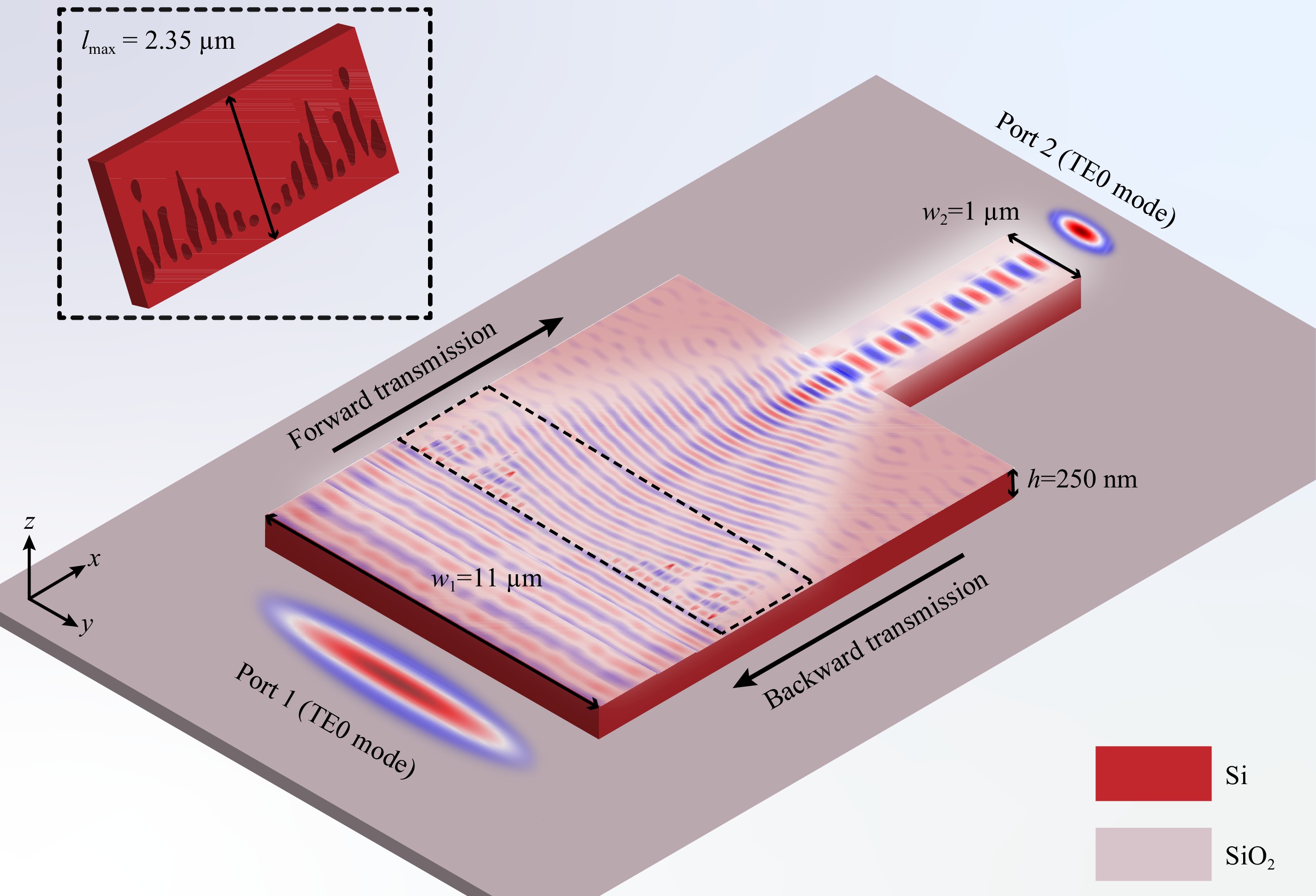
Fig. 1 Working principle of on-chip metalens for optical interconnection between wide waveguide of 11 μm to narrow waveguide of 1 μm (for TE0 mode, forward transmission allows for high-efficiency focusing, and backward transmission achieves 69% transmission efficiency of TE0 mode with well collimated phase plane; inset: structure of optimized on-chip metalens).
$$ \phi \left( {x,y} \right) = - \frac{{2\pi }}{\lambda }\left( {\sqrt {\left( {{x^2} + {y^2}} \right) + {f^2}} - f} \right) $$ (1) where (x, y) are the coordinates of each meta-atom, f is the focal length, and λ is the design wavelength.
To avoid the local optimum or saddle points encountered during the optimization process when the optimization algorithm is initiated with a random structure, the initial structure in this study was obtained using the conventional phase-matching method (refer Refs. 4 and 20), which significantly improves the optimization efficiency and reliability of the results. Here, the initial metalens structure was first defined on an SOI substrate with silicon waveguide of 250 nm thickness. The widths of the waveguides for the different ports were 11 μm and 1 μm. The widths and lengths of the rectangular air slots were used to modulate the transmission phase of each meta-atom. When light travels a distance l in the waveguide, the cumulative phase of the electromagnetic wave is expressed as:
$$ \varphi = {n_{{\text{eff}}}}{k_0}{{l}} $$ (2) where neff is the effective refractive index of the medium and k0 is the wave number in free space. Thus, for different lengths of meta-atoms in the x-direction, the phase difference of the electromagnetic wave can be calculated as:
$$ \Delta \phi = {{{k}}_{{\text{solt}}}}{{l}} + {{{k}}_{{\text{slab}}}}\left( {{l_{\max }} - l} \right) $$ (3) where l is the length of the specific slot, lmax is the length of the metalens along the x-direction, and ksolt and kslab are the effective wave numbers of the TE0 mode in the slot region and silicon slab, respectively. As shown in Fig. 2a, we used rectangular air slots defined on a 250 nm thick silicon substrate as the meta-atoms. The period was set to 500 nm, which is slightly smaller than the equivalent wavelength inside the waveguide. The period of the meta-atoms ensures that high-order diffraction is avoided, and simultaneously improves the manufacturability of the metalens. Both the amplitude and phase of the transmitted guided wave can be modulated by the width (w) and length (l) of the air slots. The high refractive-index contrast between the silicon and silica (>2) allows for a 2π phase shift at short distances. Fig. 2b shows the effects of the width and length of the rectangular air slot on the phase modulation of the TE0 mode. As the length increases, there is a gradual increase in the number of phase orders that cover the range 0–2π within a width of [0, 3.5] μm. Increasing the width of the slot had a similar effect on the number of phase orders as increasing the length. When the width was 0.03 µm and air slot was 3.5 µm, phase shift of 2π was achieved. However, when the width was increased to 0.3 µm, only 0.8 µm of etch length was required to cover the 2π phase. As shown in Fig. 2c, an increase in the slot width quickly decreases the transmission of the TE0 mode because the guided wave will scatter to free space through the slot. The change in the transmittance was particularly evident when the width of the slot was greater than half the period. Finally, we determined the width of the meta-atom to be 150 nm, as shown in Fig. 2d, which could achieve a phase shift of 2π in the length range of 0–1.5 μm, while maintaining high transmittance (~90%). Notably, using a larger air slot width can result in a phase shift of 2π at a shorter length but at the expense of device transmittance. The electric field distribution of the transmitted TE0 mode through the slot is illustrated in Fig. 2e, f. Based on the aforementioned analysis, we can achieve the desired wavefront by changing the length and width of the rectangular slots to achieve optical interconnections from wide to narrow waveguides.
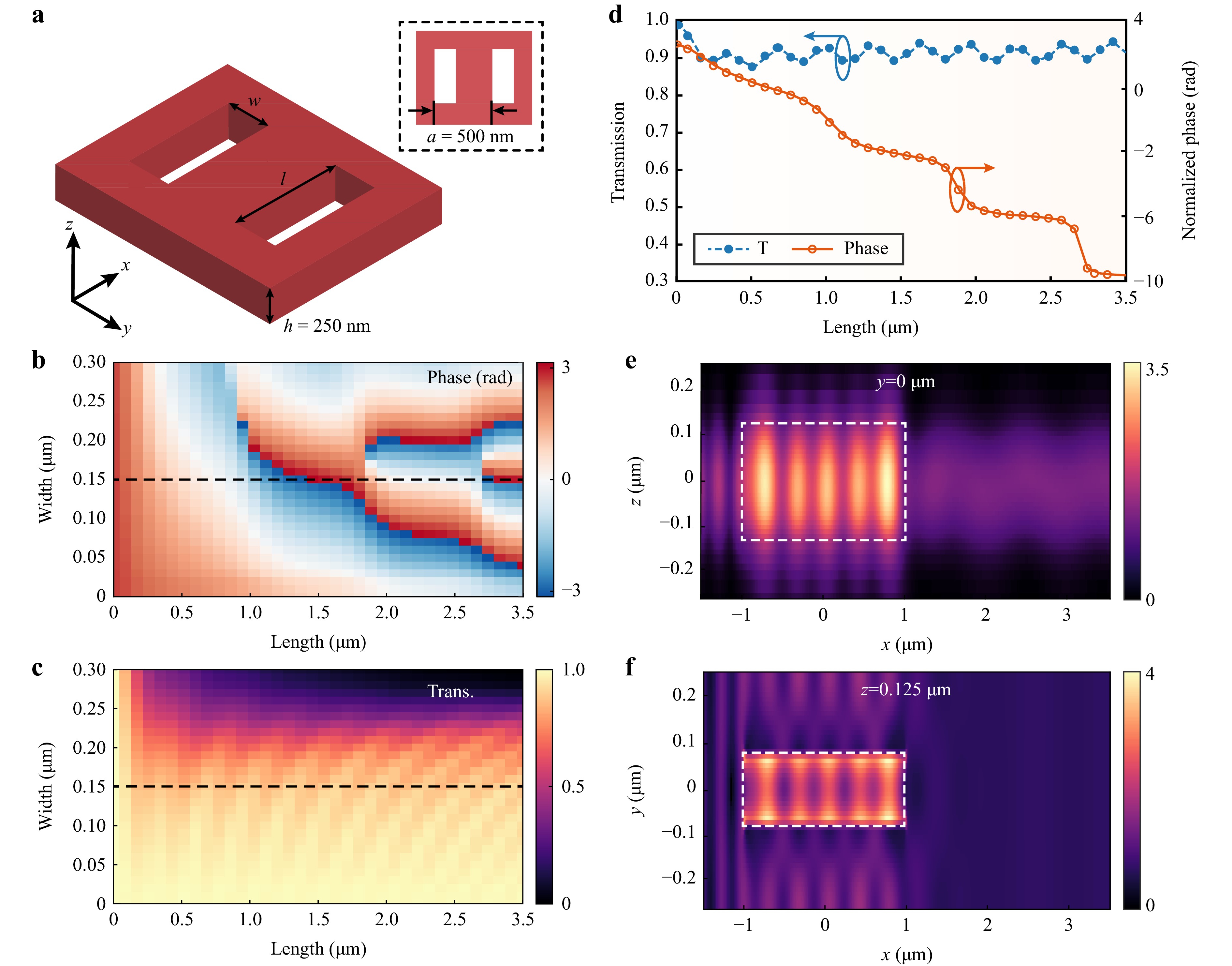
Fig. 2 Design principle of meta-atoms: a Schematic of meta-atoms defined as rectangular air slots etched on an SOI substrate of height 250 nm and period along the y-axis of 500 nm, varying the length of the air slot in the x-axis direction provides a local phase shift on an electromagnetic wave propagating in the plane; b, c numerical simulation of effect of length (l) and width (w) of air slot on phase modulation and transmission efficiency; d numerical simulation of phase and transmittance versus length of etched rectangles, fixing the width (w) to 150 nm; e, f light field intensity (represented by |Ey|2) distribution in x-z and x-y planes, dashed part indicates the etched rectangular air slot.
As mentioned earlier, the local approximation method based on periodic boundary conditions leads to larger design errors and ultimately lower transmission efficiency of the device because it neglects the gradient coupling effect in the actual arrangement of meta-atoms. Herein, we used the device obtained by the traditional design method as the initial structure and used a topology-shape optimization algorithm to solve the effect of the boundary condition so that we could obtain a more efficient device similar to the fabricated one. In our definition of the topology optimization algorithm, the objective function FoM is defined as the integral of the electric field strength in the target region as follows:
$$ E = \int\limits_\chi {f\left( {{{E}}\left( {{x}} \right)} \right)} {d^3} $$ (4) where χ is the target optimization region, and E is the electric field strength in the target region. The optimization algorithm changes the shape of the structure in the target region, such that the effective refractive index of the medium changes, which in turn leads to a change in the dielectric constant and ultimately changes the intensity of the electric field in the target optimization region. The optimized design of the on-chip metalens can be achieved through the following four steps. First, the device is updated according to the binarized spatial distribution of the refractive index. Second, the optimized area is blurred, spatial distribution of the blurred 2D structure is obtained, and electromagnetic simulation software is used to simulate the full device through the time-domain finite difference method to obtain the forward field and backward field distributions of the optimized area. Finally, the spatial distribution of the structure is updated according to the gradient, and the structure is optimized iteratively until the local optimal solution is obtained. For the adjoint method, the forward and adjoint simulation sources were the TE0 mode and ideal electric distribution on the focal plane, respectively. The ideal electric distribution on the focal plane was calculated by applying the vector diffraction theory to the ideal phase. The ideal phase distribution is described as Eq. 1. For detailed and general study of the adjoint method and more complex figures of merit, refer Ref. 67.
-
Using the aforementioned theories and design method, we designed a free-form on-chip metalens with the dual functions of focusing and collimation, finally controlling the device dimension to 11 × 2.35 μm2. Herein, we define the TE0 mode transmitted from wide to narrow waveguides as forward transmission and TE0 mode transmitted from narrow to wide waveguides as backward transmission. After optimization, the relative efficiency reached 96% when the TE0 mode propagated in the forward direction. The absolute focusing efficiency is defined as the ratio of the light intensity from the focal spot to the incident intensity, which can also be calculated as the product of the transmission and relative efficiencies of the device. The relative focusing efficiency is defined as the ratio of the light intensity from the focal spot to that from the focal plane. Utilizing the vector diffraction theory and aforementioned definition, the relative focusing efficiency was 90.2% for the ideal metalens. If it is assumed that the metalens used has a transmittance equal to that of the optimized metalens (73.2%, considering the leakage out and reflection of the free-form structure), the absolute focusing efficiency is 68.7%.
Fig. 3a presents the typical structure of a free-form metalens designed using topology-shape optimization method, which was optimized based on the initial structure designed by the conventional method, making the shape boundary of the meta-atoms nonintuitive. The intervals between each structure exceeded 200 nm, and independent structures exhibited bending radius exceeding 50 nm. In Ref. 68, the minimum feature size of silicon, which could be achieved using the electron-beam lithography method was 40 nm, which is smaller than the proposed minimum feature size (50 nm). For single-device fabrication, we adopted the following fabrication steps. The devices were fabricated on an SOI substrate with a 250 nm silicon device layer. Free-form grating patterns were written using an electron-beam lithography system with ZEP as the resist. Then, inductively coupled plasma etching was used to completely etch the Si layer. However, wafer-level fabrication requires additional constraints to regulate the characteristic dimensions based on the specific processing requirements of commercial manufacturers. As shown in Fig. 3b, during the optimization process, the forward transmission efficiency of the device gradually increased with the number of iterations. After 50 iterations of topology-shape optimization, the relative efficiency increased to 96% and absolute efficiency increased to 66%, both of which were approximately 15% higher than the efficiency of the initial structure. The transmission in the TE0 mode is the mode purity of the TE0 mode, which is also the absolute efficiency. Therefore, the mode purity of TE0 for forward transmission was 66%. The decrease in absolute efficiency after the 20th iteration may be caused by the binarization procedure in the topology-shape optimization process. The topology-shape-optimized metalens exhibits a more accurate modulation of the electromagnetic wave phase, with a smoother phase shift and large amount of light shifting toward the central axis of the waveguide (orange curve in Fig. 3c). As shown in Fig. 3d, a comparison of the electric field intensity before and after optimization illustrates that the topology-shape optimization improves energy utilization. The optimized electric field intensity was more concentrated at the central axis of the waveguide and rapidly decreased in energy on both sides away from the central axis. Conversely, the stray light on either side of the centre axis was pronounced without optimization. These results further indicate that topology-shape optimization can enhance the efficiency of the device and improve the utilization of input electromagnetic wave energy.
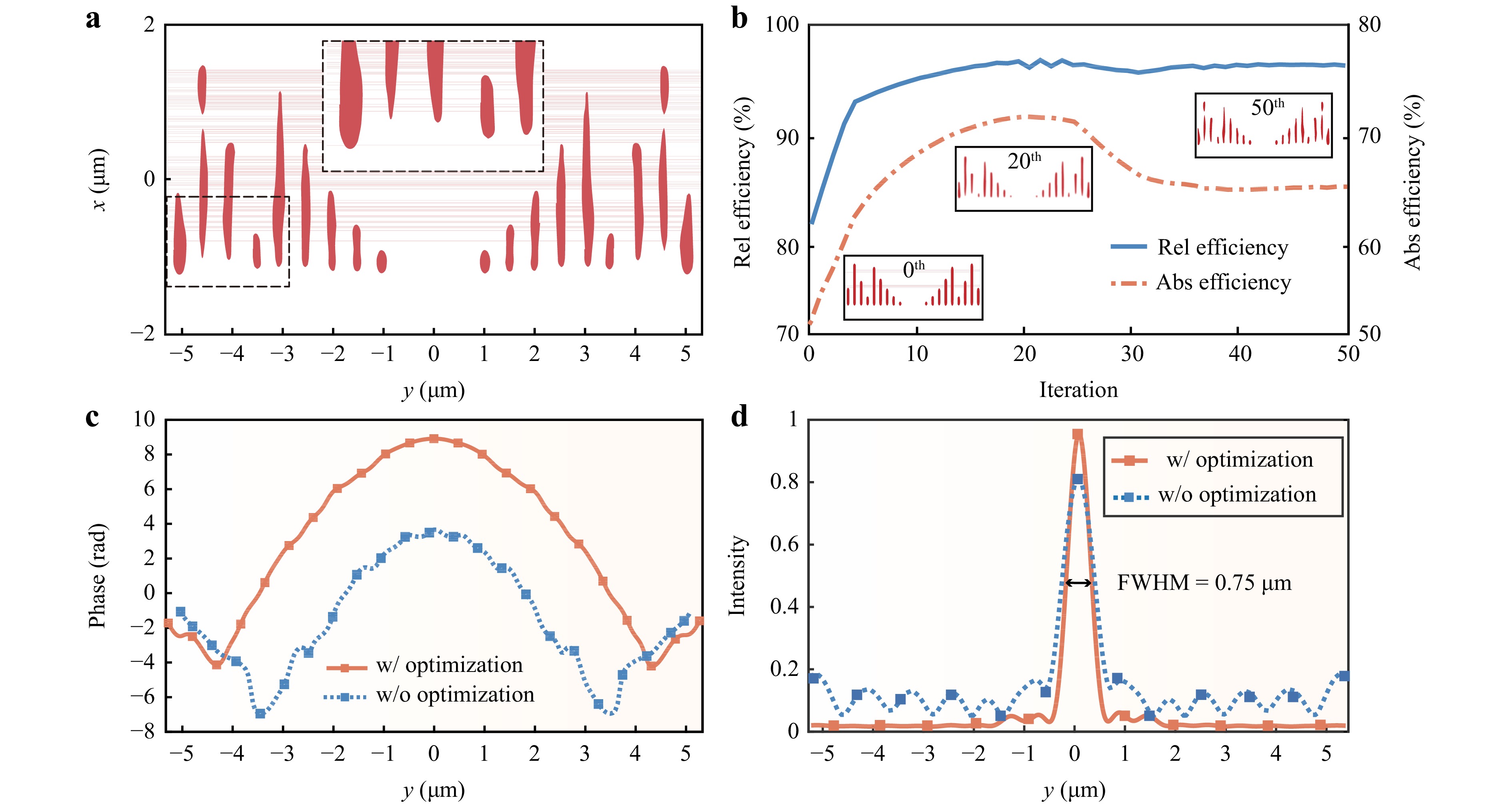
Fig. 3 Topology-shape optimized structure: a Schematic of final optimized structure; b evolution of transmission efficiency with the number of iterations (inset: topological shape distributions of 0th, 20th, and 50th iterations; c phase distribution along y direction (x = 2 μm, z = 125 nm); d electric intensity distribution along y direction (x = 10 μm, z = 125 nm), where the optimized metalens has a FWHM of 0.75 μm.
For the focusing mode, we compared the electric field distribution and electric field intensity before and after optimization. Fig. 4a, b show the optical intensity distributions in the x-y plane for the on-chip metalens obtained using the phase-match method and topology-shape optimization, respectively, in which the optimized device has less stray light as the light enters the narrow waveguide. The real y-component of the electric field clearly shows that the device obtained with periodic boundary conditions has a large amount of stray energy on both sides of the central axis during the transmission to the guided wave. Although it can transmit light from a wide to a narrow waveguide, it causes unnecessary energy dissipation and reduces the transmission efficiency of the device. By comparing the electric field distribution shown in Fig. 4c with the electric field intensity distribution shown in Fig. 4d, we found that the optimization algorithm could approximate the actual electric field distribution to the ideal distribution, and a large amount of energy converged at the focal point, resulting in a more ideal focal spot at the ideal focal length and a longer depth of focus. Fig. 4e, f show the electric field intensity distributions before and after optimizations. As can be seen from the electric field intensity distribution shown in Fig. 4f, the intensity increases steeply at the focal point, indicating that a large amount of light enters the narrow waveguide, which greatly reduces the energy loss during transmission, and thus improves the efficiency of the device. The tensity gradually decreases after the focus may result from the conversion of the focused wave with FWHM = 0.75 μm (Fig. 3d) to the fundamental TE mode of the 1 μm-wide waveguide. The output TE0 was stable, as indicated by the electric field shown in Fig. 4d.
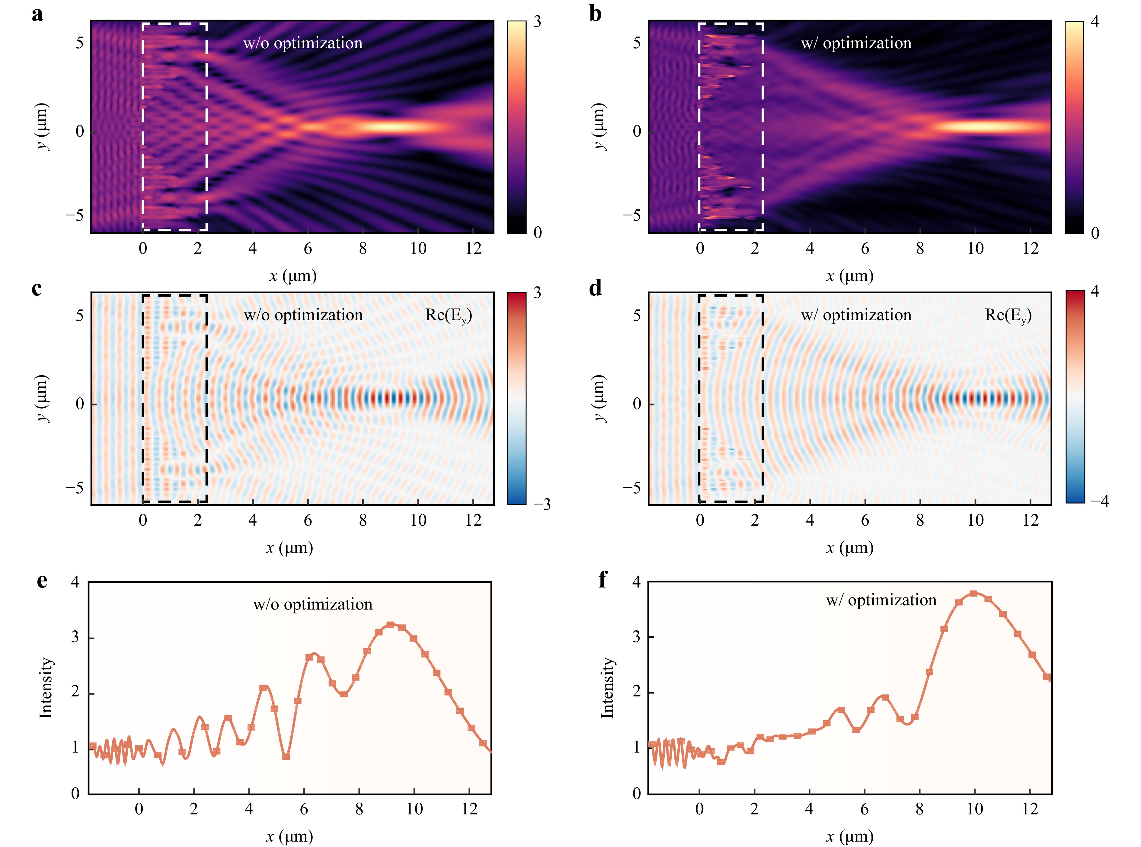
Fig. 4 Simulated field distribution of metalens before and after optimization; dashed part is the device; a, b simulated optical intensity distribution of metalens before and after optimization; c, d real part of y-component electric field before and after optimization; e, f variation in electric field intensity along x-axis before and after optimization (y = 0 μm, z = 125 nm).
For the focusing mode, Table 1 summarizes a performance comparison of the proposed free-form metalenses with those of previously reported studies. It was observed that free-form metalens with topology-shape optimization could achieve efficient light transmission at the shortest distance for high width scaling ratios. For the collimated mode, the optimally designed metalens maintained the transmission of the TE0 mode well even when the light was incident from backward (along the x-direction transmission). Fig. 5a, b present the real part of the y-component electric field for the traditional waveguide taper and optimized metalens, showing that our metalens can collimate the input light as the waveguide changes from narrow to wide. As shown in Fig. 5c, the free-form metalens maintained good transmission of the TE0 mode light as the waveguide width changed from narrow to wide (backward transmission), with a transmission efficiency of 69% at the wavelength of 1550 nm. In contrast, the traditional waveguide taper hardly transmits the TE0 mode light (transmission efficiency < 10%). In the same-material system (SOI), the main loss difference in a metadevice is its structural profile. The waveguide taper suffers from losses induced by the edge structures, whereas losses in the on-chip metalens are primarily caused by scattering and reflection. Therefore, the total transmittance of the metalens (orange solid line) is lower than that of the waveguide taper (blue solid line).
Design λ (μm) f (μm) Transmission (%) Width scaling ratio NA Waveguide taper19 1.55 15 ~91% 10/0.5 1.10 Waveguide taper54 1.55 34.2 94.70% 10/0.5 0.50 Waveguide taper55 1.55 26.3 70% 10/2 0.65 Waveguide taper with focusing lenses53 1.55 22.5 95.40% 10/0.5 0.75 PNAs OML43 1.58 16 39.8~63% 8/0.7 0.84 Dielectric GG-OML4 1.55 25 90% 11/0.5 0.75 Our work 1.55 10 96% 11/1 2.03 Table 1. Performance comparison of waveguide taper and metalens in focus mode
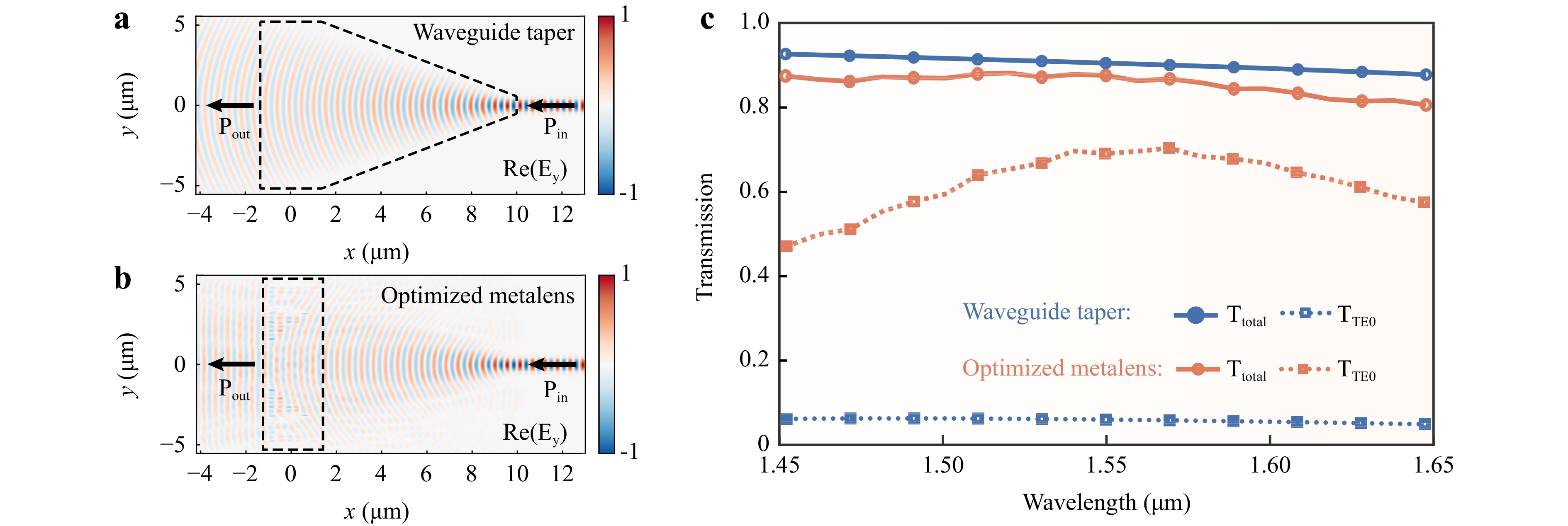
Fig. 5 Transmission of TE0 mode light by device in collimated mode: a real part of y-component electric field inside traditional waveguide taper; b real part of y-component electric field passing through the proposed device; both images in a and b are plotted with z = 125 nm; c total transmittance of all modes of light and TE0 mode light transmittance.
Owing to the improved inverse transmission effect, the designed device can ensure the generation of an equiphase wavefront in the directional radiator, thereby improving the quality of the beam radiation and reducing the noise of the system during operation. We simulated the application of the proposed device to a directional radiator. As shown in Fig. 6a, a series of radiation antennas were embedded in our silicon waveguide to radiate the light carrying the phase information into free space. Fig. 6c, d show the far-field projections of the beam with and without the metalens, respectively, where ux and uy are the direction unit vector coordinates in the far-field projection. Because our metatlens brings an equiphase wavefront, the collimated light is radiated at the same angle in the far-field projection, whereas the uncollimated light exhibits significant scattering in the far-field. The intensity of the light field versus the y- axis for both the cases is shown in Fig. 6b (at ux = 0.175). The results indicate that the intensity of the uncollimated light was significantly reduced. Fig. 6f shows the relationship between the wavelength-shift angle of the collimated far-field radiation, which is shifted by 10° at 1550 nm, and the intensity, which is more concentrated than that in Fig. 6e. It can be seen that the metalens proposed in this study has potential applications in LiDAR, optical phased arrays, directional transmission, etc.
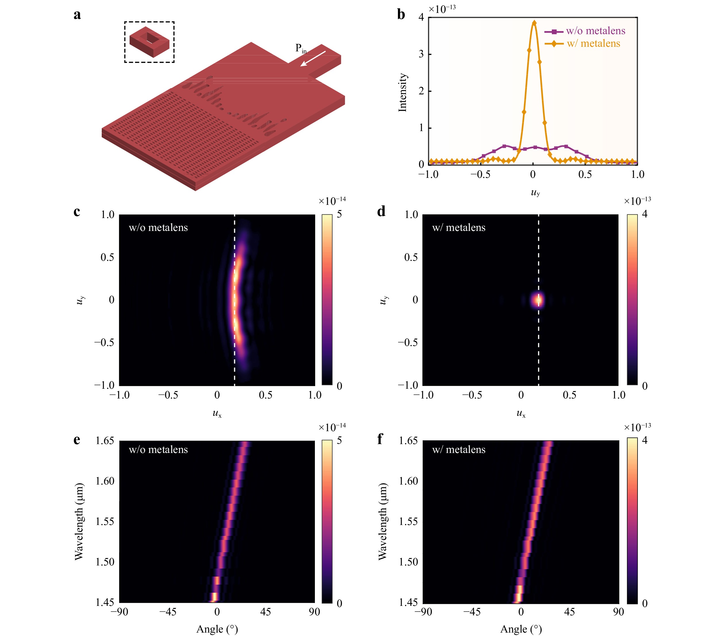
Fig. 6 Simulation of collimation patterns of devices in directional radiator (ux and uy are the direction unit vector coordinates in far-field projection); a antenna array embedded in the device, inset: cell of the array; b optical field intensity versus uy for far-field projection (yellow line is the collimated light, purple line is the uncollimated light, with ux = 0.185); c far-field projection of guided wave without collimation; d far-field projection of guided wave after collimation by our metalens, with the spot focused at 10°; e, f uncollimated and collimated guided wave in far-field projection, wavelength versus offset angle (uy = 0).
-
In conclusion, by controlling the propagating phase of a guided wave through a free-form metalens, we demonstrated an on-chip optical interconnector based on the topology-shape optimization algorithm. The proposed metalens was designed and verified numerically to focus the forward input guided wave at a distance of 10 µm with loss of less than 1 dB, while maintaining high efficiency transmission of more than 69% for the TE0 mode light when the light is propogating in the backward direction. This represents a significant advancement in the state of PICs for metalenses, which have traditionally been limited by design methods. Furthermore, we showed that an optical phase array with a tailored structure could achieve high-efficiency radiation. The designed metalens enables many on-chip systems with low losses and ultracompact dimensions, including on-chip optical information processing, on-chip spectrometers, and imaging systems.
-
This research was funded by the National Key Research and Development Program under Grant 2021YFA1401000, National Natural Science Foundation of China (NSFC) under Grants 62222513 and U20A20217, and Postdoctoral Science Foundation of Sichuan under Grant J22S001.
High-fidelity mode scaling via topological-optimized on-chip metalens for compact photonic interconnection
-
Yingli Ha1, 2,
 ,
, - Lijun Wang1, 3,
- Yinghui Guo1, 2, 3,
- Mingbo Pu1, 2, 3,
- Fang Zou4,
- Xiong Li1, 3,
- Yulong Fan1,
- Xiaoliang Ma1, 3,
-
Xiangang Luo1, 3, *, ,
- Light: Advanced Manufacturing 4, Article number: 20 (2023)
- Received: 28 February 2023
- Revised: 28 June 2023
- Accepted: 28 June 2023 Published online: 18 August 2023
doi: https://doi.org/10.37188/lam.2023.020
Abstract: Photonic integrated circuits (PICs) have attracted significant interest in communication, computation, and biomedical applications. However, most rely on highly integrated PICs devices, which require a low-loss and high-integration guided wave path. Owing to the various dimensions of different integrated photonic devices, their interconnections typically require waveguide tapers. Although a waveguide taper can overcome the width mismatch of different devices, its inherent tapering width typically results in a long length, which fundamentally limits the efficient interconnection between devices with a high scaling ratio over a short distance. Herein, we proposed a highly integrated on-chip metalens that enables optical interconnections between devices with high width-scaling ratios by embedding a free-form metasurface in a silicon-on-insulator film. The special geometric features endow the designed metalens with high coupling efficiency and high integration. The device has a footprint of only 2.35 μm in the longitudinal direction and numerical aperture of 2.03, enabling beam focusing and collimation of less than 10 μm between devices with width-scaling ratio of 11. For the fundamental transverse electric field (TE0) mode, the relative transmittance is as high as 96% for forward incidence (from wide to narrow waveguides), whereas the metalens can realize wavefront shaping for backward incidence, which can be used in optical phase arrays. This study provides new ideas for optical interconnect design and wavefront shaping in high-integration PICs. Our design approach has potential applications in directional radiators, LiDAR, on-chip optical information processing, analogue computing, and imaging.
Research Summary
on-chip metalens : compact photonic interconnection
Metalenses have been introduced into photonic integrated circuits in recent years to achieve on-chip photonic interconnects, providing an opportunity to solve the problem of low optical interconnect efficiency between relatively large-scale devices. Xiangang Luo from Chinese Academy of Sciences now report development of a highly integrated on-chip metalens that enables optical interconnection between devices with a high width scaling ratio by embedding a free-form metasurface in a silicon-on-insulator film. The special geometric features by inverse design endow the designed metalens with high coupling efficiency and high integration. The device has a footprint of only 2.35 μm in the longitudinal direction and a numerical aperture (NA) of 2.03, enabling beam focusing and collimation in less than 10 μm between devices with a width scaling ratio of 11.
Rights and permissions
Open Access This article is licensed under a Creative Commons Attribution 4.0 International License, which permits use, sharing, adaptation, distribution and reproduction in any medium or format, as long as you give appropriate credit to the original author(s) and the source, provide a link to the Creative Commons license, and indicate if changes were made. The images or other third party material in this article are included in the article′s Creative Commons license, unless indicated otherwise in a credit line to the material. If material is not included in the article′s Creative Commons license and your intended use is not permitted by statutory regulation or exceeds the permitted use, you will need to obtain permission directly from the copyright holder. To view a copy of this license, visit http://creativecommons.org/licenses/by/4.0/.

 DownLoad: