


-
Two-photon polymerisation lithography (TPL) is an advanced fabrication technology with the ability to generate three-dimensional (3D) structures at print resolutions of the order of hundreds of nanometers1–7. Continued progress in this technology has led to the 3D printing of advanced optical elements, including mode sorters8, imaging optics on fibre facets9–13, and corrective phase elements14. In addition to beam-shaping components, subwavelength structures that can control the phase and amplitude of light have also been realised15,16. Bioinspired structural colouration has been realised via the microscopic printing of structures such as photonic crystals, nanocavities, nanodiscs, and nanopillars17–26. Precise control over the nanostructural geometry is essential for accurately tuning the generated colour. TPL has streamlined the fabrication of such nanostructures owing to its high resolution and capability to control the exposure dose at each point. Although a range of saturation, hue, and brightness has been achieved using different techniques for colour generation27, realising inherently absorptive structures to absorb stray light instead of scattering it remains a formidable challenge.
Greyscale and full-colour pallets have been achieved by scattering light from 3D-printed nanopillars at the single-nanopillar level27. Short nanopillars that effectively scatter a broad range of wavelengths appear black with minimal transmittance in the visible spectral range within a narrow acceptance cone. Because such structures exhibit minimal light absorption, they are less suitable for large-area masking applications that require opaque and absorptive 3D structures. Processes for generating a non-transparent area in the optical element for optical applications have been demonstrated using multiple wafer-level techniques28–30 involving deposition, lithography, and etching processes, which require precise alignment methods and a stringent process control. In previous studies, translucent structures have been fabricated using digital light processing printers and extensive post-processing techniques31. A technique to selectively 3D print opaque surfaces will be valuable for applications that require light blockage in particular areas, such as apertures and slits integrated with other complex optical components, to reduce the effect of stray light and improve contrast. To date, masking has been achieved by 3D printing transparent hulls and then filling the internal cavities with black ink to render them opaque32,33. Such fabrication techniques can create perfectly opaque structures with smooth surfaces but require a separate manual process for filling ink carefully into the cavities, with the accompanying risk of ink spillage onto the transparent optical component.
In this study, we investigated the laser decomposition conditions for TPL to create well-defined opaque domains in a transparent optical component. The laser dose can be tuned to control the characteristics of polymers, such as the polarity of the resist34 and the refractive index of the polymerised structures35, in laser lithography. Exposing the TPL resins to laser intensities above a threshold results in laser-induced decomposition of the material owing to a sharp increase in the local temperature of the laser-irradiated area36. This temperature rise creates bubbles that affect printing and damages intricate structures37. Hence, laser decomposition is typically avoided in TPL owing to its random nature. The current work was inspired by the observed opacity of the decomposed structures. We investigated whether the observed opacity could be controlled to create uniform opaque patches in an optical element. Controlling the laser decomposition process can facilitate the single-material-based fabrication of transparent and opaque structures in a single optical component. To the best of our knowledge, this is the first study that achieves the opacity of an optical element as printed without any post processing. Realising such selective opacity can be valuable for the single-step fabrication of alignment-free fully 3D-printed apertures and other light-blocking structures for optical components.
-
Opaque structure fabrication through TPL is a sequential process for defining each area in the optical design by controlling the laser dose, as depicted in the schematic of the 2 × 2 checkerboard pattern in Fig. 1. First, the transparent areas in the design are fabricated using a suitable laser dose for crosslinking the resin (see Methods section for details). This process leaves a resin pool confined within a shell/contour in designated opaque regions. Subsequently, in-fill structures are fabricated in the resin pool to confine the liquid resin to smaller volumes. In-fills are vertical planes in the x and y directions that divide the unpolymerised resin into smaller pools. Finally, the smaller resin pools are subjected to layer-by-layer high-dose laser irradiation. The in-fill structures minimise the movement of microscopic cavitation structures and hinder their coalescence into larger bubbles that interfere with the printing process. Infill planes also serve as a support to the contour, preventing it from collapsing during the temperature rise under laser exposure and developmental stages. The structures in this study were fabricated using a commercial TPL system (Photonic Professional GT) from Nanoscribe GmbH, using the proprietary photoresist IP-S and a 25× objective, although the approach can be extended to process most organic resins.
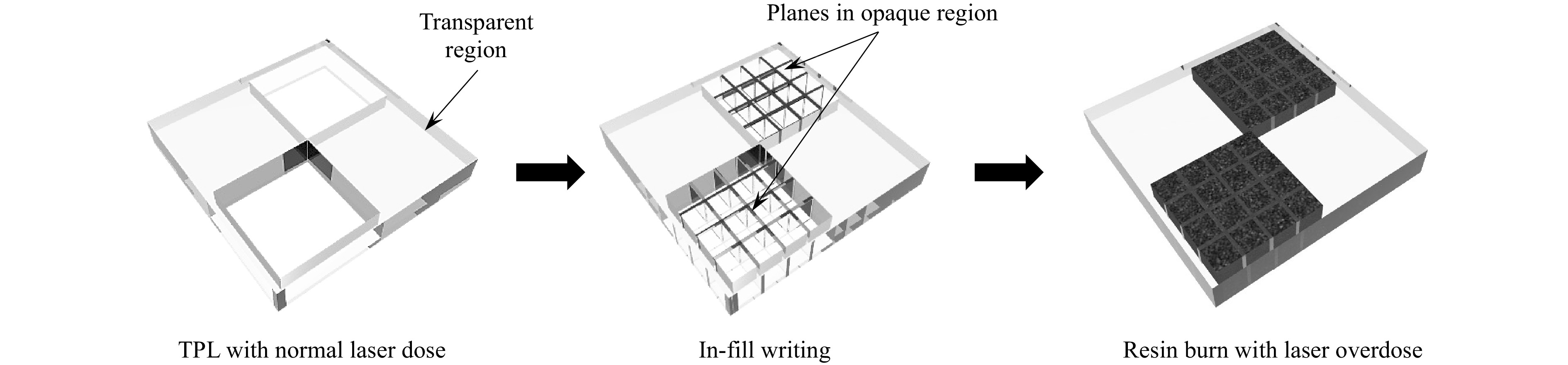
Fig. 1 Schematic of a sequential overexposure process. Transparent regions in the design are first printed via TPL using regular exposure conditions. To control the laser decomposition process, the regions selected to be opaque are first printed with in-fill structures, after which the entire volume is overexposed at laser powers that are sufficient to induce resin decomposition. The resulting structures exhibit opacity in the overexposed regions.
Overexposed regions patterned using the parameters detailed in the Methods section produced solid structures with different levels of structural damage and opacity (Fig. 2a). In general, when patterned above the threshold laser power, lower scan speeds and corresponding higher dwell times resulted in increased bubble formation and material decomposition. The uniformity of material decomposition and the opacity of the laser-irradiated area depended on the laser dose, which is directly proportional to the laser power (LP) and inversely to the scan speed (SS). The Photonic Professional GT system used in this study had an average power of 66 mW at 100% LP, a repetition rate of 80 MHz, and a resulting pulse energy of 0.825 nJ or a peak intensity of ~2 TW/cm2 (assuming a Gaussian spot diameter of ~1 µm and ~100 fs pulse duration). As expected, resin crosslinking occurred under the conditions of 80% LP and 10,000 µm/s SS, resulting in the printing of transparent structures. When the LP was increased to 100% while maintaining the SS at 10,000 µm/s, partial resin damage was observed. The observed opacity was non-uniform, resulting in some areas that were fully transparent and others partially opaque. Upon decreasing the SS to 5000 µm/s at 100% LP, the structure appeared to be fully damaged with a more uniform opacity, compromising the overall form. To determine the optimal laser dose that triggers the damage process, point array exposure was performed, in which the laser beam was pulsed and focused to polymerise the individual voxels (Fig. 2b). At lower doses, the exposed spots were perfectly formed without any aberration. The size of the spots formed varied according to the laser dose. When the LP was increased, the dwell time or exposure time required to initiate damage decreased (Fig. 2c).
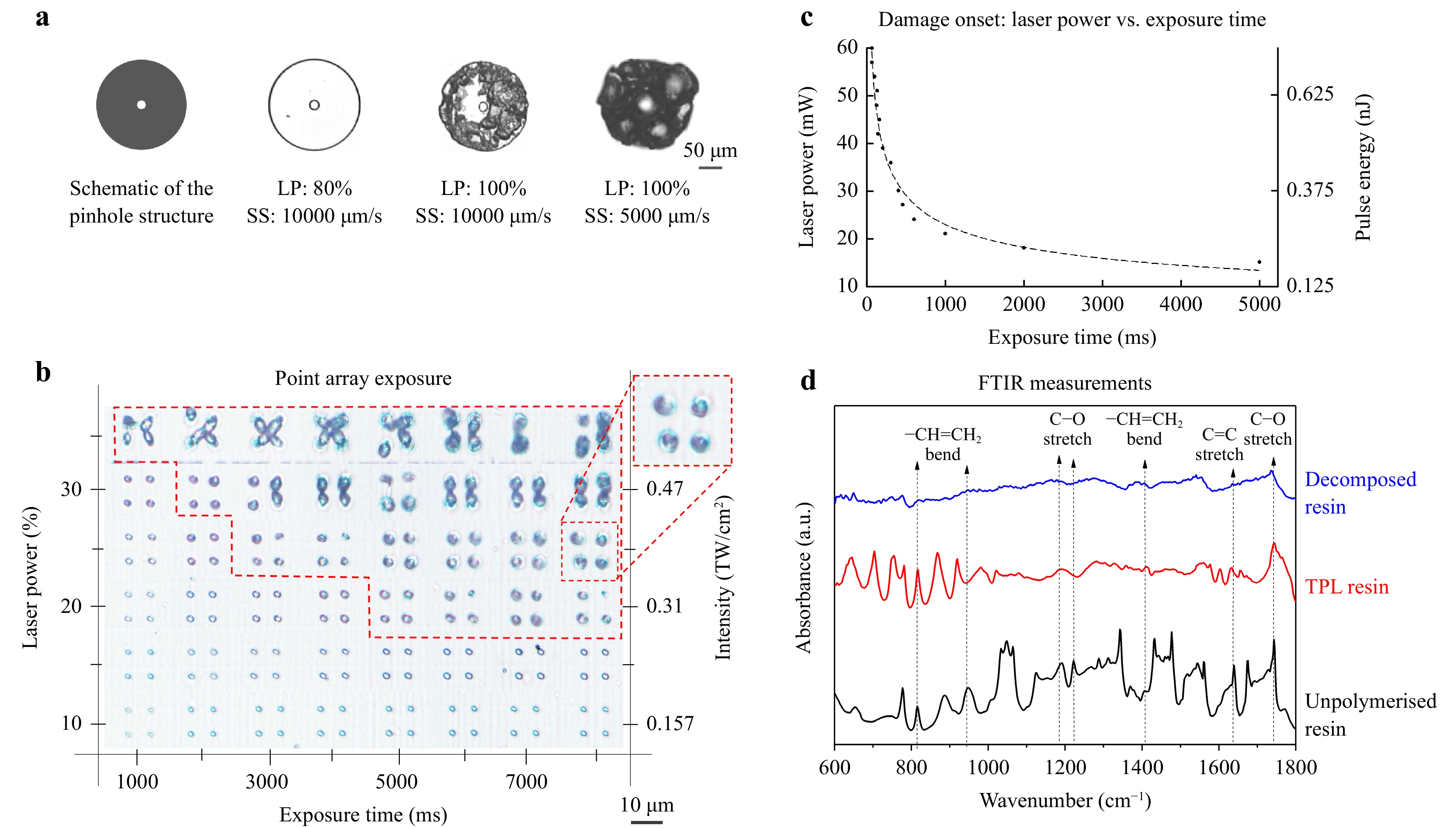
Fig. 2 Evaluation of the laser decomposition process. a Schematic and microscopic images of a targeted pinhole structure. Undesirable random structures were produced upon simply increasing the laser dose, i.e. increasing the laser power (LP) or reducing the scan speed (SS). b Optical micrographs (100×) illustrating point array exposure to evaluate the onset of damage. Points treated with a lower dose are well defined whereas those treated above the threshold dose are deformed, indicating the onset of laser damage (Inset: representative damaged structures). c Critical laser power vs. the exposure time at the onset of laser decomposition. d FTIR spectra of the IP-S resin (non-polymerised, polymerised, and decomposed) over the molecular fingerprint region of 600 to 1750 cm−1.
Fourier transform infrared (FTIR) spectroscopy was used to obtain the IR transmittance spectra of the materials based on the interaction of the resin molecules with the incident radiation. Different samples provided different spectra, as molecular vibrations are unique to the material and hence are considered as a ‘fingerprint’ of the material. A Vertex 80V FTIR spectrometer (Bruker Optik GmbH) was used to evaluate the degree of polymerisation of the IP-S resin, which was composed of a carbamate-methacrylate mixture constituting >95% of the resin, with the remainder being butyrolactone (<5%) and a photoinitiator based on aromatic ketones (<1%). According to this composition, the IP-S resin contains C=O and CH2=CH− functional groups38. Characteristic vibrational bands associated with CH2=CH−, C=O, C=C, and C-O groups were detected in the wavenumber range of ~600–1750 cm−1, which is the molecular fingerprint region in the FTIR spectra, as shown in Fig. 2d. The band intensities were normalised to that of the C=O band. The C=C stretching band at ~1635 cm−1 and its bending modes at ~810 and ~940 and ~1410 cm −1 are shown in the spectra. Compared with that of the unpolymerised resin, the percentage of C=C decreased by 50% for the TPL-polymerised sample, whereas it was negligible for the fully decomposed sample, as determined from the C=C bending mode at ~810 cm−1. This reduction might be due to the conversion of C=C into C-C, that is, the carbonisation process, which led to the darkening of the irradiated area.
Following the observation of the random opacity of the decomposed structures, we evaluated various writing strategies to comprehensively understand the process to achieve uniformity: 1) Single-step overexposure: a computer-aided design model was fabricated with high-dose exposure of the entire structure. This resulted in non-uniform opacity, and structural deformations occurred along the boundaries owing to bubble formation (Fig. 3b). 2) Multistep exposure with a pre-polymerised resin: as bubble formation and movement in a liquid resin were found to hinder the fabrication process in the single-step exposure strategy, we adopted a writing sequence in which the intended structure was first written using an appropriate laser dose to induce the polymerisation of the resin. The polymerised area was subsequently overwritten with a higher laser dose to cause material damage and thus create opacity. However, once polymerised, the structures tended to remain stable, withstanding high laser doses and surviving the high laser energy with minimal damage (Fig. 3c, d). The results of this multistep exposure experiment suggested that laser damage can be predominantly induced only in the non-polymerised resin volume. 3) Sequential exposure: in this process, the area that needs to be opaque was first defined by writing the contour. The liquid resin puddle within the contour was then exposed to a high laser dose to induce material decomposition. Although the overall structure was maintained in this writing strategy, the opacity was non-uniform (Fig. 3e). We then modified the sequential exposure step to include the in-fill inside the resin puddle to confine the liquid resin to smaller pools and minimise the effects of bubbling. This process resulted in a well-defined structure with uniform opacity, as shown in Fig. 3f.
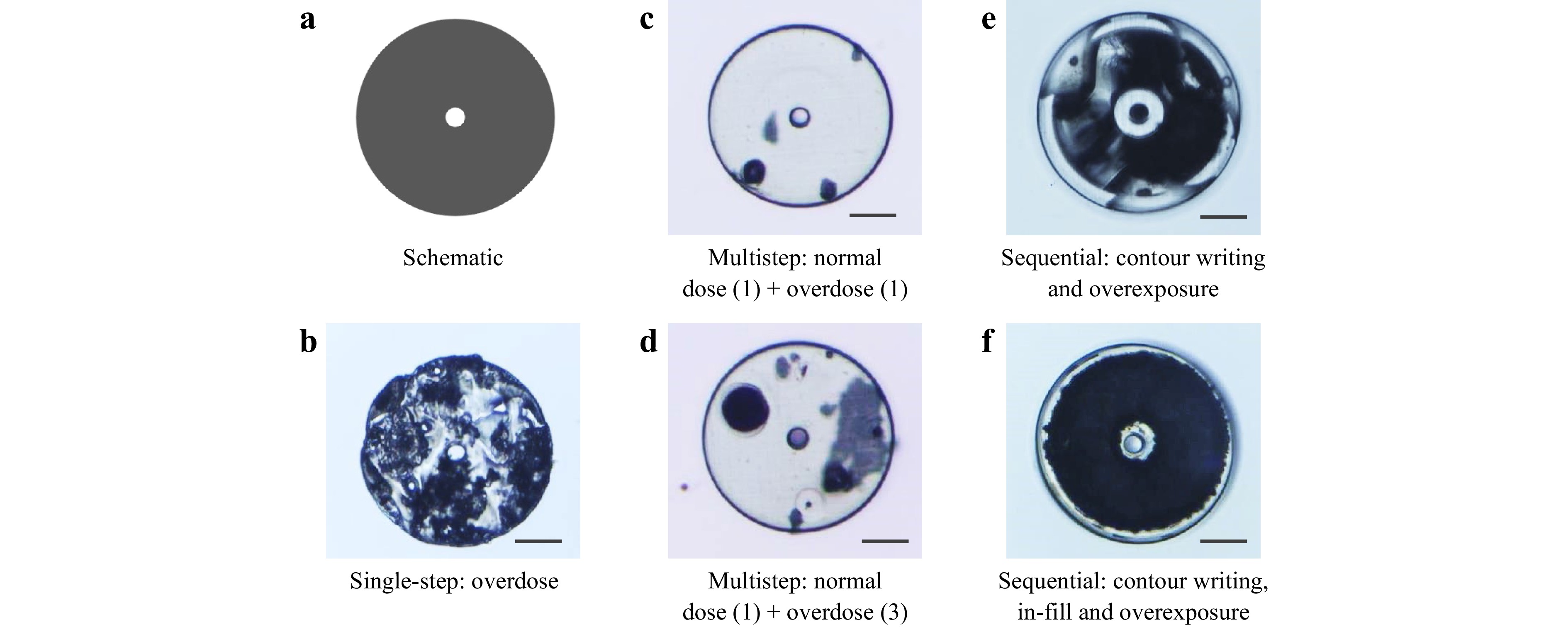
Fig. 3 Fabrication processes to achieve opacity a Schematic of the pinhole design. b−f Optical micrograph of the b structure obtained with a single-step laser exposure under overdose conditions, c structure fabricated through multistep exposure: first exposure with normal dose and second exposure with overdose, d structure fabricated through multistep exposure: exposure with normal dose followed by overdose exposure of the same area for three cycles, e pinhole fabricated with sequential exposure (contour written first and inner areas overexposed next), and f pinhole fabricated with sequential exposure (contour writing followed by in-fill fabrication in inner areas and overexposure of the inner areas). Scalebar: 50 µm.
Previous studies have suggested that laser decomposition of the material mainly occurs because of the increased absorption of laser energy in the vicinity of pre-existing features. The energy absorbed by the liquid resin near pre-existing features is higher, because the polymerised and cured resins absorb single-photon near-IR radiation37. This energy absorption causes laser decomposition to occur predominantly in the liquid resin medium at high laser doses. During laser decomposition, bubbles are formed in the resin pool owing to localised heat accumulation. We observed that the bubbles moved around during the laser passes, resulting in random material decomposition. We also observed that such randomness was prominent for large-area exposure, and the minimum feature size that could be achieved with laser decomposition in our process was ~10 µm (Fig. S1).
Efforts to minimise the effect of bubbling resulted in the development of an in-fill-based overexposure process. When the opaque area was subdivided into smaller resin pools with infills/scaffolds, the damage was confined to smaller volumes, and the bubbles formed were small and had a minimal effect on the overall structure. Furthermore, we speculated that heat dissipation was reduced owing to numerous liquid–solid interfaces, which aided local heat accumulation. The checkerboard pattern fabricated with scaffolds (Fig. 4a) depicts the efficacy of the infill-based writing process in defining alternating transparent and opaque areas. The transmission properties of the opaque structures were characterised using a Nikon Eclipse LV100 ND optical microscope equipped with a CRAIC 508PV microspectrophotometer with a 20× objective and a numerical aperture of 0.45. The transmittances of the glass and transparent resin were also measured for reference (Fig. 4b). The opacity of the laser-decomposed structure depended on the structural thickness. The transmittance of the opaque structures fabricated by laser decomposition decreased with increasing structural thickness. Square patches with heights varying from 10 to 100 µm were fabricated, and their transmission was evaluated. Moreover, multiple patches with the same thickness were tested to ensure repeatability and analyse the uncertainties of the measurements. As shown in Fig. 4c, The average minimum transmittance was approximately 14% (Fig. 4c). The error bars indicate multiple thicknesses at which the transmittance can be minimised, with the lowest being 30 µm. Abstract black and white patterns were printed with a thickness of 50 µm Fig. 4d(i) to evaluate the fabrication process for obtaining realisable geometries with curved shapes and sharp corners. Multiple prints of the same pattern were tested to ensure repeatability. The interface between the dark and light regions printed using alternating laser exposure had an average roughness of 4.3 µm along the edges. The 3D-printed coffee mug shown in Fig. 4d(ii) demonstrates the ability of the process to fabricate true 3D opaque structures. The top row of Fig. 4d(ii) shows a schematic of an empty mug, half-filled mug, and fully filled mug. The transmission microscopy images of the fabricated structures corresponding to the design are shown in the bottom row.
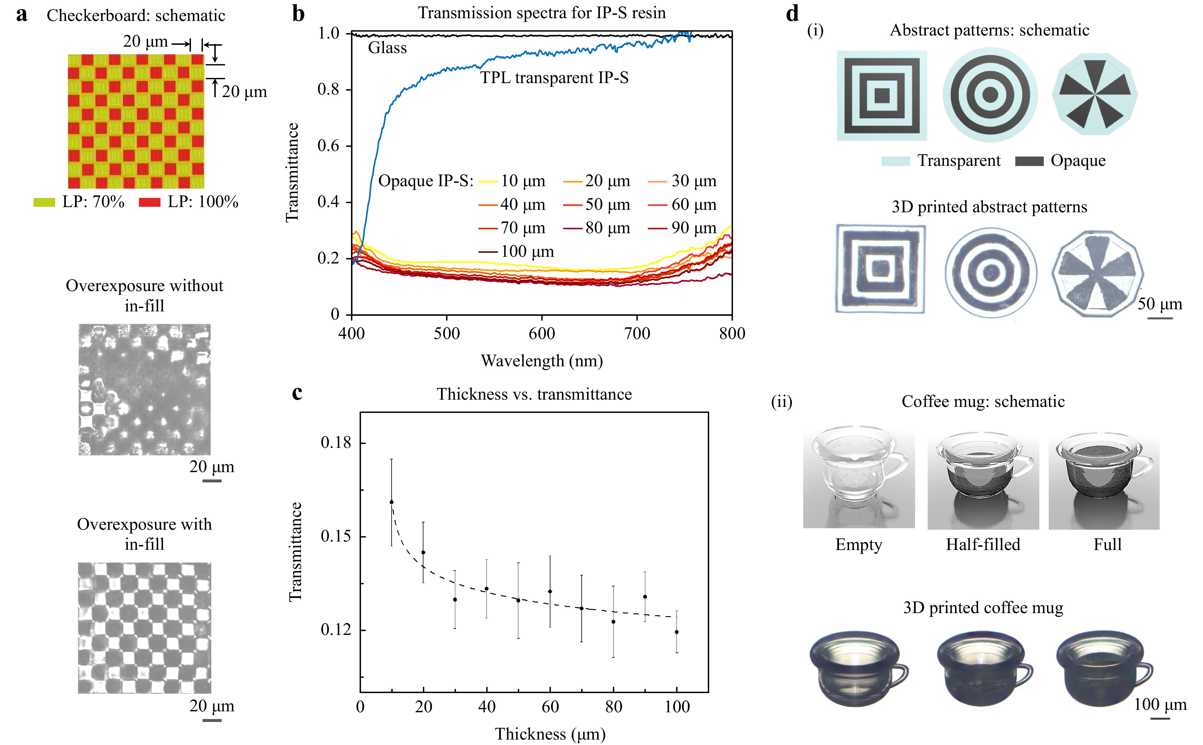
Fig. 4 Selective opaque structure fabrication. a Schematic and optical micrographs of a checkerboard pattern printed with and without in-fills. b Visible-light transmission spectra of opaque structures of different thicknesses. Two photon-polymerised structures were transparent and had a transmittance approaching that of glass for wavelengths above 450 nm. c Average transmittances of structures with different thicknesses printed using the in-fill approach for the 425–700 nm range. Thicknesses above 30 µm consistently resulted in less than 15% transmittance. d Selective transparent and opaque structures fabricated through TPL: (i) Abstract patterns with transparent and opaque regions, (ii) 3D structures (a coffee mug: design (top) and TPL-fabricated sample (bottom); the mug was fabricated with crosslinking laser dose and the ‘coffee’ feature was developed using the laser dose for material decomposition).
Opaque structures are relevant in optical systems for blocking specific areas and reducing the effects of stray light32. To demonstrate the effect of the masking structures, we fabricated a Fresnel lens and then created an opaque shell with an aperture using the sequential writing process detailed above to block any stray light during imaging (Fig. 5a). The shell and aperture positions were aligned with the lens and optimised in a computer-aided design model to leverage the freedom of single-lithographic step fabrication. The lens was used to image a negative USAF 1951 resolution test chart in the transmission mode on a Nikon Eclipse LV100 ND optical microscope. Fig. 5b displays the image obtained at the focal plane of the Fresnel lens. The observed intensity across the line-pair set of element 5 in group 5 was quantified from the image using MATLAB (Fig. 5c). The image contrast improved from ~9% for the Fresnel lens without an aperture to ~24% for the Fresnel lens with an opaque shell and aperture.
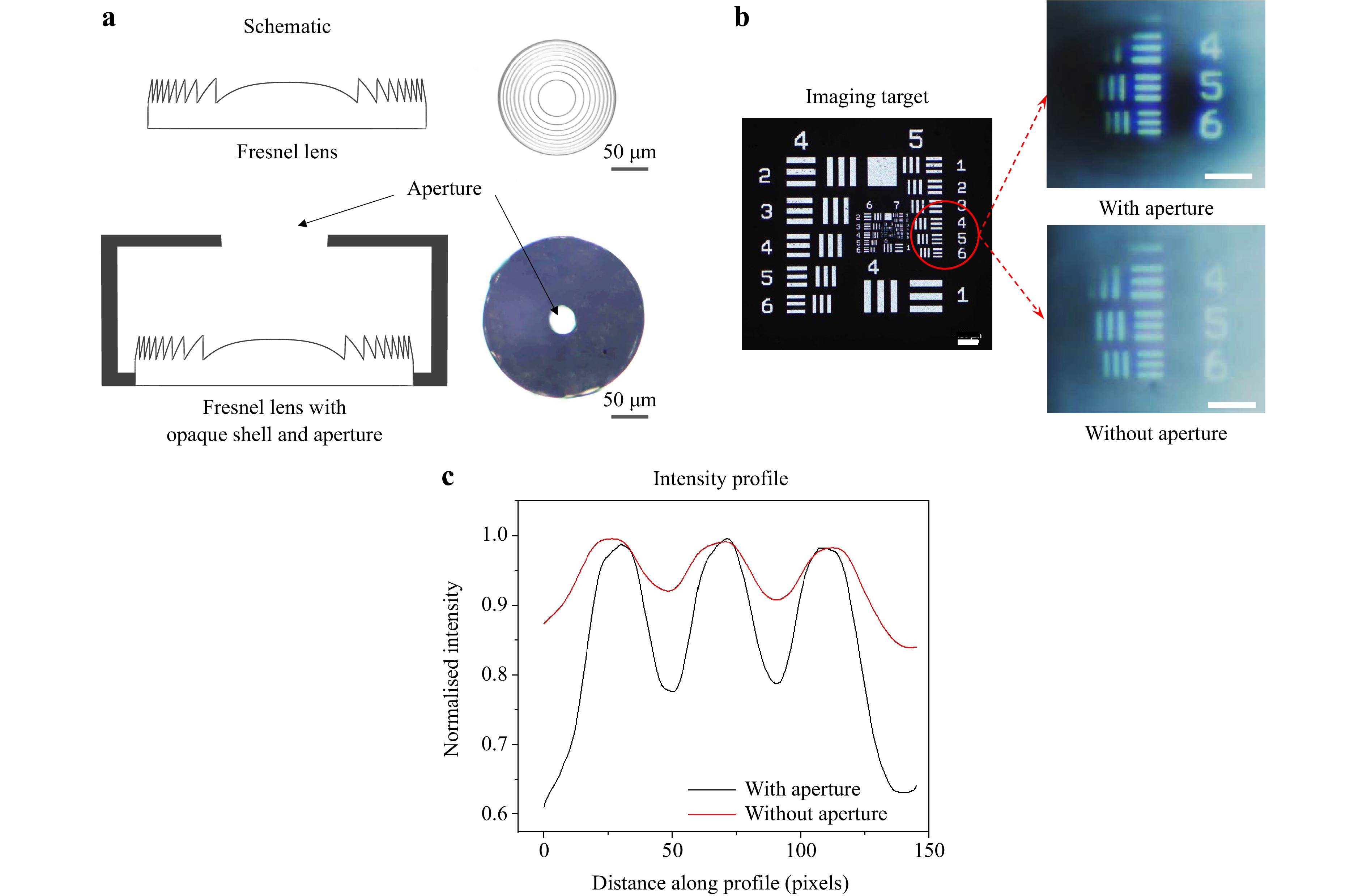
Fig. 5 Contrast improvement with an opaque shell aperture. a Schematic and microscopic image of a Fresnel lens (top) and a tilted-view microscopic image of the Fresnel lens with an opaque shell and aperture (bottom). b USAF 1951 resolution chart imaged through the Fresnel lens without and with an aperture (Scalebars: 100 µm). c Intensity profile plot along the line pair in the images obtained in b. Image intensity profile shown for element 5 of group 5.
In summary, we demonstrated a printing strategy for achieving both opaque and transparent 3D structures with a single resin using TPL. We printed opaque structures using a high laser power to induce laser decomposition of the liquid resin within predefined microscopic compartments, realising localised heat accumulation. The in-fill structures within a contour help reduce the coalescence of micro-bubbles formed during overexposure. We demonstrated the use of rectangular planes as in-fill structures. Future studies focusing on various 3D patterns and pattern densities for in-fills will be required to define the finest features that can be rendered opaque and to further reduce the transmittance of the opaque structures and enhance resolution. These opaque structures can be defined alongside transparent structures by modulating the laser exposure conditions, thus simplifying the process to a single printing process that uses a single material. The decomposed material exhibits approximately three times higher opacity than proprietary resins39. The efficacy and practical applicability of the fabrication technique were demonstrated via the single-step fabrication of the lens and aperture, achieving a three-fold improvement in contrast for imaging applications. This study focused on masking structures, and further investigations are required for evaluating the effectiveness of the technique in fabricating intricate 3D structures in black. Although the overall structure can be maintained as designed, the reduction in the print speed by six times in opaque regions is a trade-off (see Methods), and the micron-scale roughness of the opaque regions can be further improved. Further investigations on the use of high-power lasers, resin chemistry, and exposure techniques are expected to improve the resolution and printing speed of opaque structures.
-
All the structures were fabricated using a commercial two-photon polymerisation lithography system (Photonic Professional GT, Nanoscribe GmbH). This 3D printing system uses a pulsed femtosecond laser with a peak wavelength of 780 nm, a pulse duration of 100 fs, and a repetition rate of 80 MHz. The proprietary resin, IP-S, and a 25× objective with a numerical aperture of 0.8 were used in the fabrication of both transparent and opaque structures reported in this work. The IP-Dip resin exhibited similar damage and opacity characteristics. Opaque regions were divided into smaller resin pools of 10 µm × 10 µm dimensions (Fig. S2) using in-fill planes of 1 µm thickness. The depth of the resin pool was maintained at the same height as the designed structure. Once the pools were defined, the liquid resin in the pool was exposed to an overdose of laser with a layer thickness defined by the slicing distance. The laser beam was programmed to move to the next pool after polymerising one layer from the previous pool. Once a layer was exposed in all the pools, the stage holding the substrate shifted the z-position based on the slicing distance, and the beam was moved again to the first pool to irradiate the next layer. Pool hopping and layer polymerisation were continued until the entire resin pool was exposed. The optimal slicing and hatching distances for the structures fabricated with the IP-S resin were 1 µm and 500 nm, respectively. However, to facilitate a local temperature increase for resin damage and opacity, it is essential to maintain closer laser passes within a structure. Hence, a slicing distance of 500 nm and a hatching distance of 200 nm were used for forming opaque structures. An LP of 70% and an SS of 50,000 µm/s (referred to as the ideal laser dose in the main text) were used to fabricate transparent structures at a printing rate of 2700 µm3/s. On the other hand, opaque structures were fabricated using 100% LP and 5000 µm/s SS (referred to as overdose in the text) with a print time of 460 µm3/s. The uncured resin was removed by immersing in polyethylene glycol methyl ether acetate (30 min), isopropyl alcohol (5 min), and nonafluorobutyl methyl ether (5 min). Previous studies have demonstrated the fabrication of optical components based on inorganic materials for high-temperature applications40. Structures demonstrated in this work were characterised under ambient conditions. Although the organic resin material used in this study is known to have a degradation temperature of 300 °C41, further investigations are required to define the robustness and behaviour of the opaque structures under extreme temperature conditions.
-
This work was funded by the Singapore University of Technology and Design (SUTD) through the SUTD Ph.D. Fellowship. We would like to thank the Singapore University of Technology and Design (SUTD) cleanroom for providing fabrication facilities.
Fabrication of opaque and transparent 3D structures using a single material via two-photon polymerisation lithography
-
Parvathi Nair Suseela Nair1, *, ,
 ,
, - Chengfeng Pan2,
- Hao Wang2,
- Deepshikha Arora2,
- Qing Yang Steve Wu1,
- M. A. Rahman2,
- Jinghua Teng1,
-
Joel K. W. Yang1, 2, *, ,
- Light: Advanced Manufacturing 4, Article number: (2023)
- Received: 06 May 2023
- Revised: 28 July 2023
- Accepted: 29 July 2023 Published online: 31 August 2023
doi: https://doi.org/10.37188/lam.2023.025
Abstract: Two-photon polymerisation lithography enables the three-dimensional (3D)-printing of high-resolution micron- and nano-scale structures. Structures that are 3D-printed using proprietary resins are transparent and are suitable as optical components. However, achieving a mix of opaque and transparent structures in a single optical component is challenging and requires multiple material systems or the manual introduction of ink after fabrication. In this study, we investigated an overexposure printing process for laser decomposition, which typically produces uncontrollable and random ‘burnt’ structures. Specifically, we present a printing strategy to control this decomposition process, realising the on-demand printing of opaque or transparent structures in a single lithographic step using a single resin. Using this method, opaque structures can be printed with a minimum feature size of approximately 10 µm, which exhibit<15% transmittance at a thickness of approximately 30 µm. We applied this process to print an opaque aperture integrated with a transparent lens to demonstrate an improved imaging contrast.
Research Summary
‘Burnt’ structures for opacity in optical applications
A 3D printing technique to fabricate opaque designs from transparent material shows promising applications in optics. Applications such as micro-imaging systems can produce high quality results with the integration of opaque structures that blinds the light in selected areas. Parvathi Nair S. from Institute of Materials Research and Engineering (IMRE), Singapore and Prof.Joel K.W. Yang’s research group from Singapore University of Technology and Design now report a process to 3D print transparent and opaque structures on micron-scale using a single transparent resin. This process can effectively replace the conventional shell filling approach, where one has to first print a transparent shell and then fill it with inks to make it non-transparent. The team demonstrated printing of several black and white designs and showed an improvement in the imaging contrast.
Rights and permissions
Open Access This article is licensed under a Creative Commons Attribution 4.0 International License, which permits use, sharing, adaptation, distribution and reproduction in any medium or format, as long as you give appropriate credit to the original author(s) and the source, provide a link to the Creative Commons license, and indicate if changes were made. The images or other third party material in this article are included in the article′s Creative Commons license, unless indicated otherwise in a credit line to the material. If material is not included in the article′s Creative Commons license and your intended use is not permitted by statutory regulation or exceeds the permitted use, you will need to obtain permission directly from the copyright holder. To view a copy of this license, visit http://creativecommons.org/licenses/by/4.0/.

 DownLoad: