


-
Integrated photonics is a discipline of integrating devices such as waveguides, lasers, photodetectors on a single chip. Owing to fast and efficient transmission and processing of information, integrated photonics holds a significant potential for applications in communication, computing, and sensing1. It offers several advantages such as low cost, low power consumption, and scalability2. Although materials like silicon3,4, silicon nitride (Si3N4)5,6, and indium phosphide (InP)7,8 have been widely used as the photonics integration platform, lithium niobate (LN) has gained considerable attention due to its strong electro-optic coefficient, large nonlinearity, and wide transparency window9. However, as a photonics integration platform, traditional bulk LN material faces several challenges such as weak mode confinement, large footprint, and reduced nonlinear efficiency10. To overcome these challenges, thin-film lithium niobate (TFLN) technique has emerged as a solution. Owing to the large refractive index difference between LN device layer and SiO2 BOX layer, TFLN technique enables tight mode confinement and high nonlinear efficiency, leading to its wide adoption in optical communications, microwave photonics, THz communications, and quantum photonics11,12.
Followed by the commercial availability of high-quality TFLN wafers and the breakthrough of its fabrication technique, TFLN technique is implemented to the development of various optoelectronics components, such as compact and high-performance modulators13-15, broadband optical frequency combs16,17, polarization management devices18, and efficient wavelength converters19,20. Most of these TFLN devices use external lasers and photodetectors since the LN material does not natively provide a light source and photodetection, a challenge faced by the TFLN technique as a potential universal photonics integrated circuits (PICs) platform12. The flip-chip bonding technique was recently applied to integrate the InP distributed feedback (DFB) laser die with a pre-fabricated TFLN modulator chip21. Low-loss and high-power TFLN-InP transmitters were achieved by optimizing the overlap between the respective platform modes. Besides, as an important optoelectronic conversion device, high-performance integrated photodiodes are essential for the TFLN integration platform. Amorphous silicon photodetectors integrated on the TFLN platform was realized within the visible wavelength range22. It features a bandwidth of 10 MHz and responsivity of 22 to 37 mA/W over the wavelengths ranging from 635 to 850 nm. Further exploration is required for photodiodes operating in the wavelength range of optical communication.
Heterogeneous integration is an effective technique to integrate active components on the chip for indirect-bandgap materials23. Several heterogeneously integrated photodiodes have been successfully developed on silicon-based platforms24-27. Recently, heterogeneous integration technique was adopted to achieve broadband photodetection on the TFLN platform28. A high-performance photodiode with 80-GHz 3-dB bandwidth and 0.6-A/W responsivity at 1,550 nm was demonstrated by using die-bonding technique, with SU-8 as the adhesion layer. Although the broadband photodetection on the TFLN platform had been enabled, an ultra-wideband photodiode with 110-GHz 3-dB bandwidth on the TFLN platform is still highly desired to advance the overall performance of the TFLN PICs, considering that the state-of-the-art TFLN modulator exhibits a 3-dB bandwidth of 110 GHz29. Moreover, TFLN technique lacks a wafer-level integration of active components, which is a major challenge to achieve a massive-scale, multi-function, and high-performance TFLN PICs. Therefore, it is of great significance to achieve wafer-level integration of ultra-wideband photodiodes on a thin-film lithium niobate platform.
This study addresses the challenge by wafer-level heterogeneously integrating InP/InGaAs modified uni-traveling carrier (MUTC) photodiode wafer onto the TFLN wafer with pre-defined waveguides and passive components. The MUTC Epi stack featured with p layers down is implemented to simultaneously boost the bandwidth and responsivity. The fabricated waveguide-coupled photodiodes based on the wafer-level TFLN-InP heterogeneous integration technique have a dark current of approximately 1 nA and a responsivity of 0.4 A/W at a wavelength of 1,550 nm. The measured 3-dB bandwidths on 50-Ω load reach up to 110 GHz, which is comparable to that of the state-of-the-art TFLN modulator. The devices are successfully applied in a four-level pulse amplitude modulation (PAM4) data-receiving system, which demonstrates the potential of the photodiodes on the TFLN platform for next-generation high-speed transmission systems.
-
Table 1 shows the Epi layer structure of the MUTC PDs, which were grown by metal–organic chemical vapor deposition (MOCVD) on a semi-insulating InP substrate. The n-doped layers were initially grown on the InP substrate to establish a p-down structure after wafer bonding. In this structure, the absorption region had a total thickness of 120 nm, consisting of graded doped absorption layers of 100 nm (5 × 1017 cm−3 → 5 × 1018 cm−3) and a depleted absorption layer of 20 nm (1 × 1016 cm−3). A self-induced electric field in the graded doped absorption layer enhanced the transport of the photo-generated electrons30. A 20-nm-thick n-doped cliff layer with 3 × 1017 cm−3 doping level was incorporated to mitigate the space charge effect31. A 120-nm-thick drift layer was chosen to balance the junction capacitance and carrier transit time. To enable electron velocity overshoot, the electric field in the drift region was regulated by inserting a p-doped sacrifice layer32. Heavily doped InGaAs and InGaAsP were used as the n and p contact layers, respectively. In addition, InGaAsP layer acted as an optical coupling layer to achieve an efficient optical coupling between the active layers and lithium niobate waveguide. After optimizing the thickness of the InGaAsP layer, a thin absorption layer could perform an effective light absorption due to the strong optical coupling. Compared to the n-down structure, our structure could achieve a high responsivity since the absorption layers were close to the LN waveguide. The LN waveguide had a total thickness of 600 nm and a slab thickness of 300 nm. The width of the LN waveguide was designed as 1 μm for a low-loss light transmission.
Layer Material Thickness Doping Substrate InP 350 μm Semi-insulating Buffer layer InP 500 nm N+ doping, 5 × 1018 cm−3 N-contact layer In0.53Ga0.47As 50 nm N++ doping, 1 × 1019 cm−3 Cladding layer InP 60 nm N+ doping, 5 × 1018 cm−3 Sacrificial layer InP 40 nm P+ doping, 1 × 1018 cm−3 Drift layer InP 120 nm N- doping, 3 × 1016 cm−3 Cliff layer InP 20 nm N doping, 3 × 1017 cm−3 Smooth layer InGaAsP 10 nm N- doping, 1 × 1016 cm−3 Depleted absorption layer In0.53Ga0.47As 20 nm N- doping, 1 × 1016 cm−3 Graded doped
absorption layerIn0.53Ga0.47As 100 nm P doping, 5 × 1017 cm−3
↓
P+ doping, 5 × 1018 cm-3P-contact layer InGaAsP 280 nm P+ doping, 8 × 1018 cm-3 Table 1. Epi structure of the MUTC PDs
Fig. 1 illustrates the designed fabrication process of the heterogeneously integrated photodiodes on the TFLN wafer, which includes wafer bonding, III-V material etching, and electrode fabrication. Initially, the LN waveguide was obtained by dry etching. The width of the fabricated LN waveguide was approximate 1 µm. The slope of the waveguide sidewall was approximate 63 degrees. Microscope and scanning electron microscope (SEM) images of the LN waveguide can be seen in Fig. 2a, b, respectively. Subsequently, an InP/InGaAs wafer was bonded onto the TFLN wafer with pre-defined waveguides and passive components. A combination of dry and wet etching techniques was utilized to etch III-V material, forming the n- and p- mesa while avoiding undercut and waveguide damage. The etched n mesa and p mesa are shown in Fig. 2c, d. Finally, a metal layer was electroplated as an electrode, as shown in Fig. 2e, f. Further details of the fabrication process can be found in the Materials and Methods section. The heterogeneously integrated MUTC PD were fabricated with the active areas of 2 μm × 6 μm, 2 μm × 8μm, 2 μm × 10 μm, 2 μm × 12 μm and 2 μm × 14 μm.
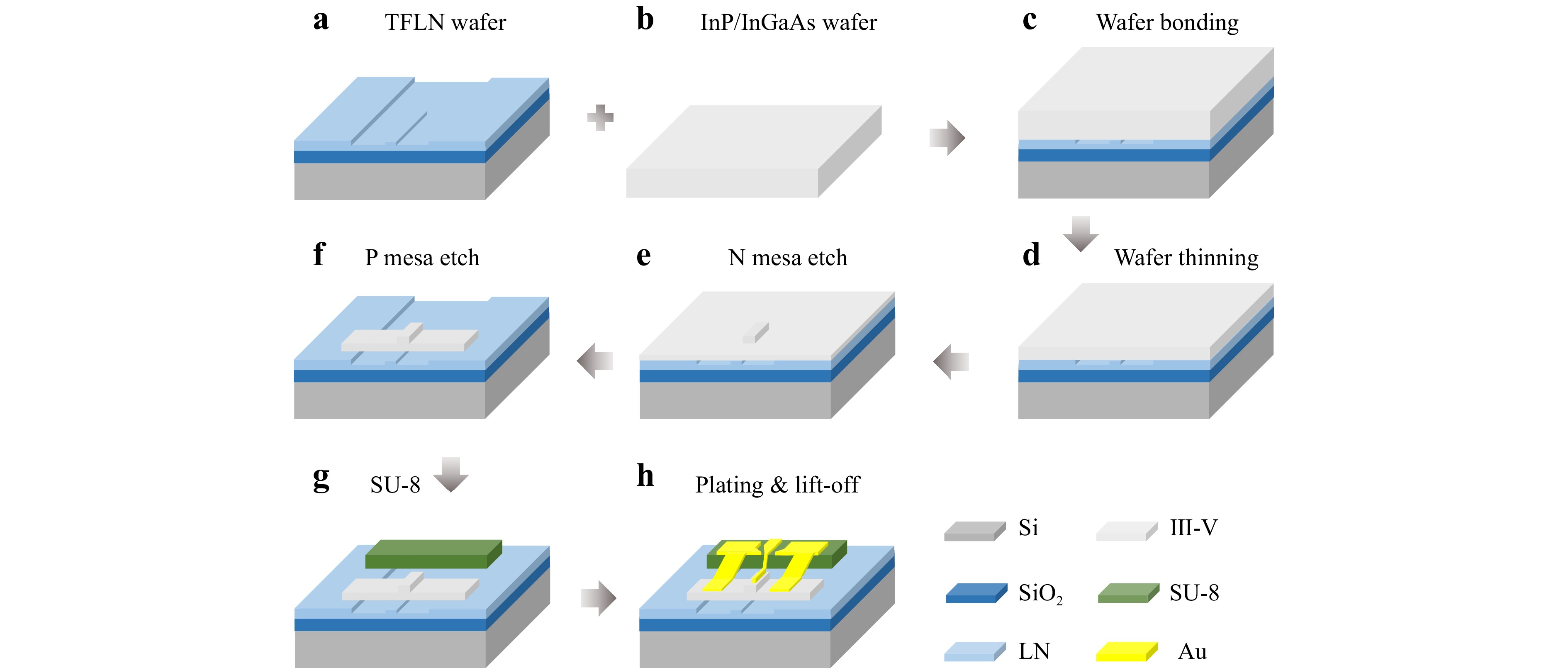
Fig. 1 The designed process flow used to fabricate the waveguide-coupled photodiodes on the TFLN platform. a TFLN wafer with pre-defined waveguide and passive components, b bare InP/InGaAs wafer, c InP/InGaAs wafer and TFLN wafer bonding, d InP/InGaAs wafer substrate removal, e N mesa etch, f P mesa etch, g SU-8 base for CPW pad, and h metal electroplating and lift-off.
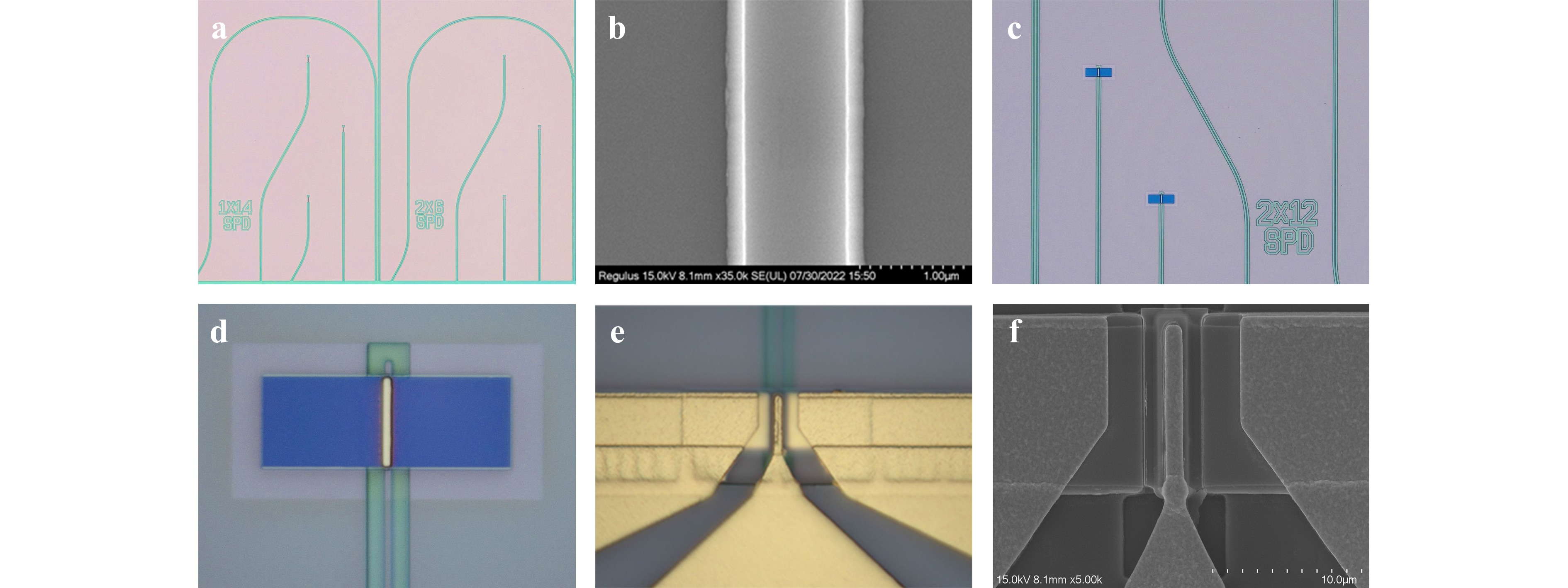
Fig. 2 Microscope a and SEM b images of the LN waveguide. c and d, microscope images of the devices after n-mesa and p-mesa etching. Microscope e and SEM f images of the fabricated photodiodes.
-
First, we measured the dark current of the fabricated PDs. Fig. 3a shows the dark current versus the bias voltage of the devices with the active areas of 2 μm × 6 μm – 2 μm × 14 μm. The typical dark current of the devices is approximately 1 nA at −4 V bias. Notably, the current at forward bias was relatively low due to the presence of the p-doped layer in the drift region. Next, the internal responsivity of the waveguide-coupled PDs was characterized. The fiber-to-waveguide coupling loss and waveguide loss were measured to calculate the internal responsivity of the devices. A lensed fiber with a spot size of 2.5 μm was used to couple the light into and out of the loopback waveguides near the target photodiodes. The coupling and waveguide propagation losses were approximately 7 dB. The photocurrent was measured by coupling light into the photodiode near the loopback waveguide. At the wavelength of 1,550 nm, the internal responsivities of the devices with lengths of 6 – 14 μm were 0.4, 0.48, 0.5, 0.54, and 0.55 A/W, considering the measured coupling and waveguide propagation losses, as shown in Fig. 3b. The measured responsivities of the devices were consistent with the simulated ones. When the PD length increased, the responsivity saturated due to the intrinsic absorption of the metal stack. The absorption of the metal stack can be mitigated by optimizing the thickness of the cladding layer.
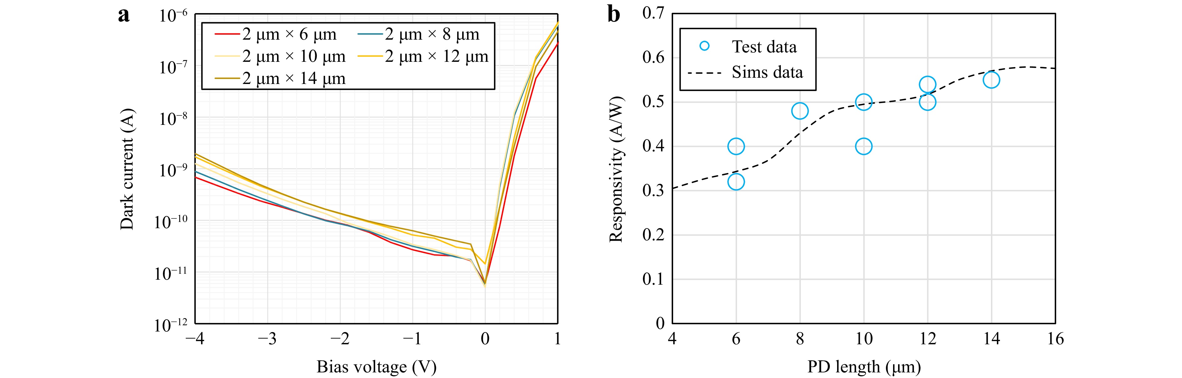
Fig. 3 a I–V curves of the devices with the active areas of 2 μm × 6 μm – 2 μm × 14 μm. b measured and simulated responsivities of the devices with lengths of 6 – 14 μm.
The S parameter of the devices was measured using a vector network analyzer with a frequency range of DC – 67 GHz. By fitting the measured S parameters to the equivalent circuit model, as shown in Fig. 4a, the resistance and capacitance of the devices were extracted. The measured and fitted S11 curves of the devices with active areas of 2 μm × 6 μm – 2 μm × 14 μm at −4 V bias voltage are presented in Figs. 4b–f. The physical parameters extracted from the measured S11 and the Lumerical 3D model are shown in Fig. 5. The fitted parameters of the devices with different active areas and lengths were consistent with the simulation results. The fabricated photodiodes on the TFLN platform exhibited low junction capacitance but a relatively large series resistance, dominated by the resistance on p-mesa.
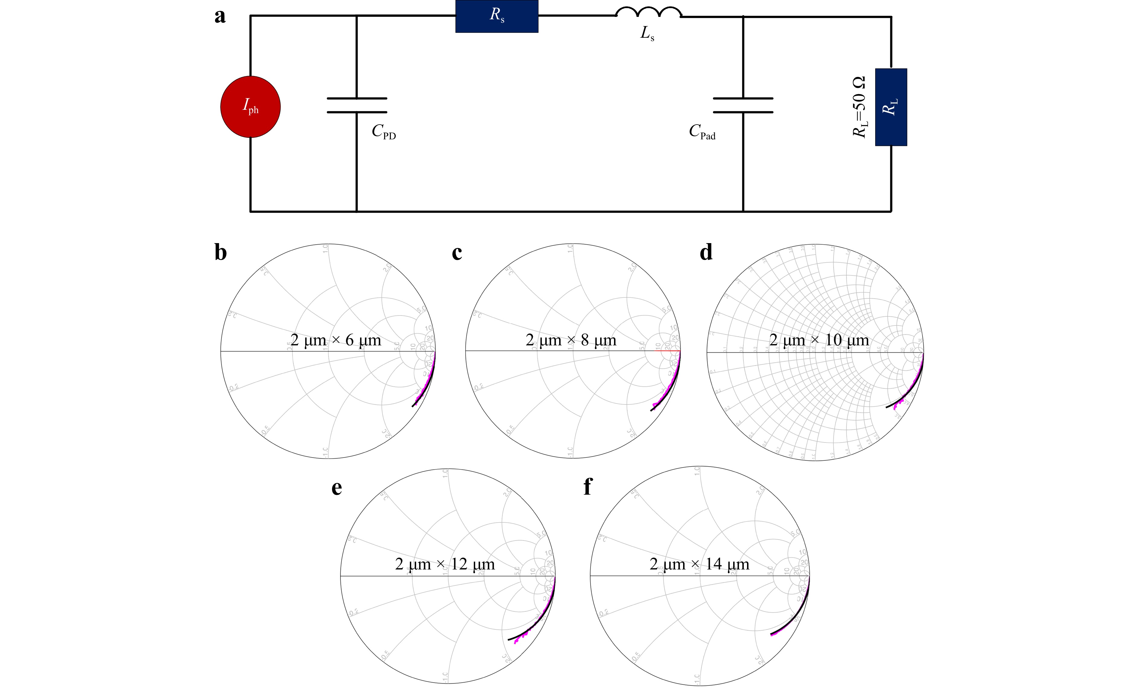
Fig. 4 a Equivalent circuit model of the devices for S11 fitting and frequency response simulation. Iph, CPD, Rs, Cpad, and Ls represents the frequency-dependent current source, junction capacitance, series resistance, and the capacitance and inductance of the CPW pattern, respectively. b–f Measured (red solid line) and fitted (black solid line) S11 curves (frequency range: 1 – 67 GHz) for devices with the active areas of 2 μm × 6 μm – 2 μm × 14 μm at -4 V bias voltage.
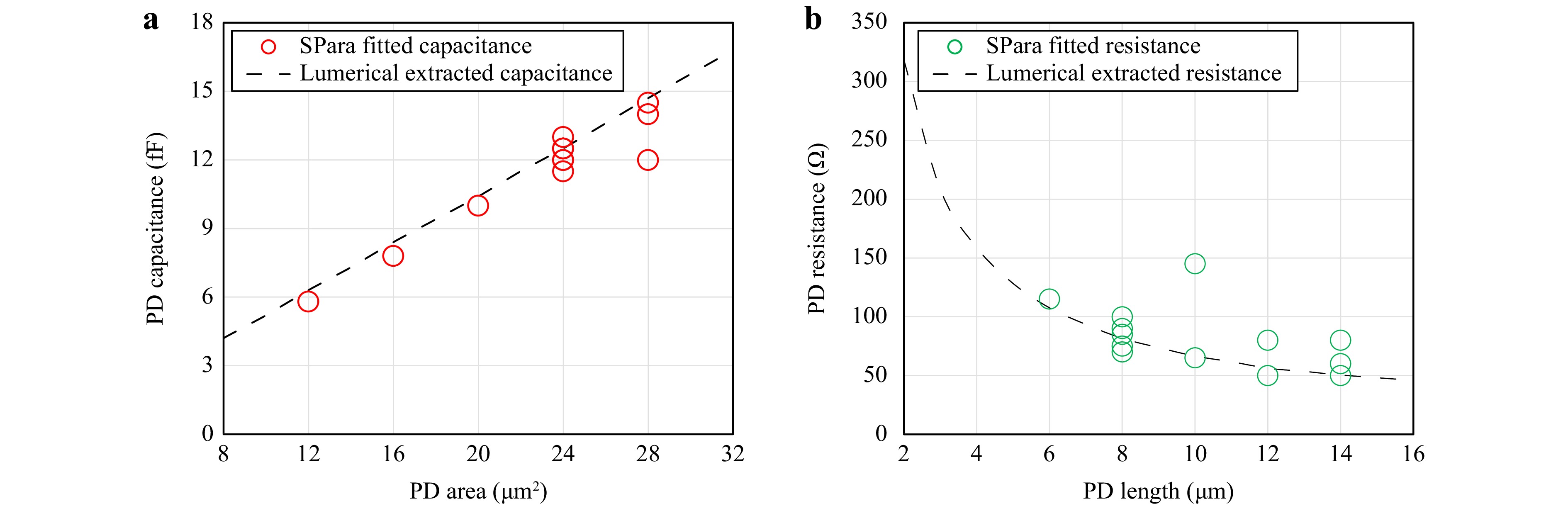
Fig. 5 PD capacitance a and resistance b extracted from the measured S11 parameter and the Lumerical 3D model.
The experimental setup shown in Fig. 6 was used to measure the frequency response of the devices. With RF probes in the frequency ranges DC – 67 GHz and 75 –110 GHz, we measured the RF power in the corresponding frequency bands. Figs. 7a–e shows the power responses of the devices with different active areas. The maximum bandwidths of the devices with the active areas of 2 μm × 6 μm, 2 μm × 8 μm, 2 μm × 10 μm, 2 μm × 12 μm, and 2 μm × 14 μm are 110, 105, 100, 101, and 97 GHz, respectively. Fig. 7f shows the simulated bandwidths (transit-time bandwidth, RC bandwidth, and total bandwidth) based on physical parameters extracted from the Lumerical 3D model and the measured bandwidths. Evidently, the measured bandwidths were consistent with the simulated results. The estimated carrier transit time was 2.9 fs, and the corresponding transit-time-limited bandwidth was 153 GHz. For the devices with active areas below 20 μm2, the bandwidth was limited by the carrier transit time. When the device area increased and became larger than 20 μm2, the bandwidth was limited by the RC constant.
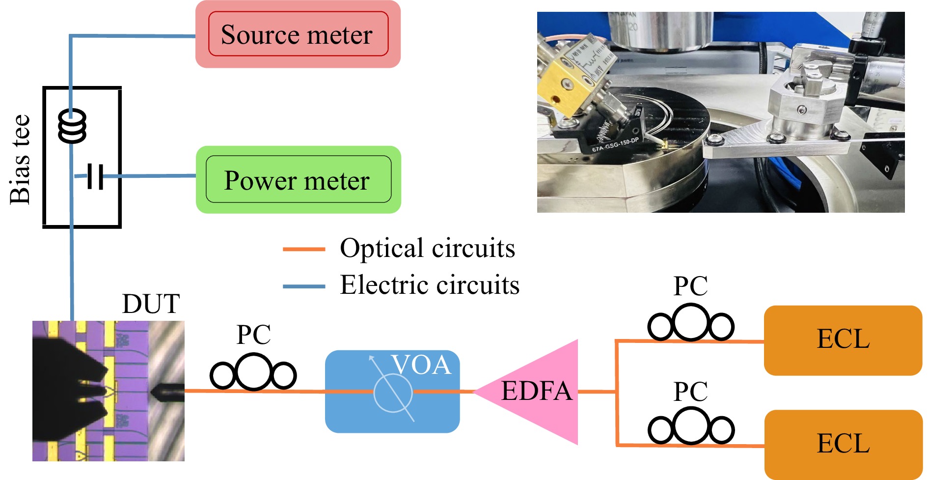
Fig. 6 Frequency response measurement setup. ECL: external cavity laser; PC: polarization controller; EDFA: Erbium-doped fiber amplifier; VOA: variable optical attenuator; DUT: device under test. The inset figure shows the experiment setup including bias tee, RF probe, fabricated chip, and lensed fiber.
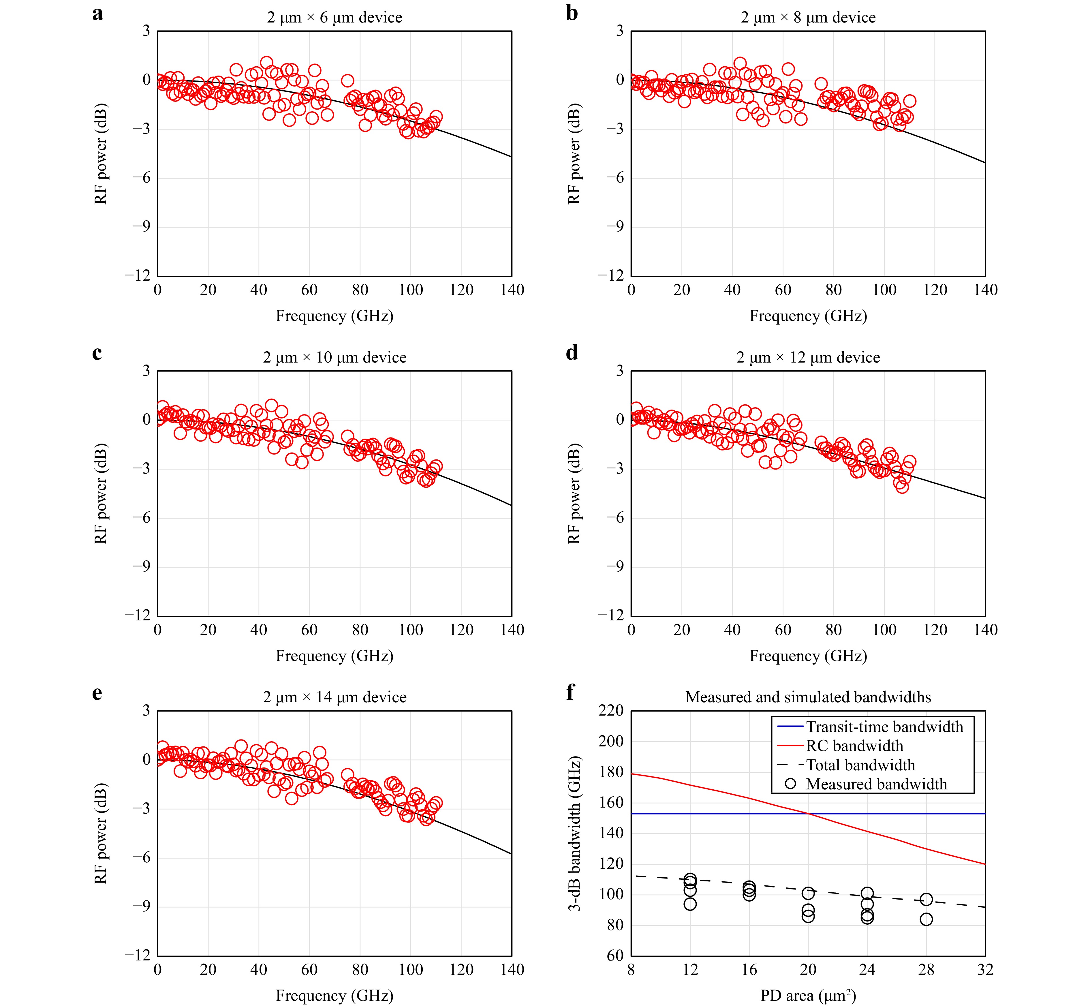
Fig. 7 Frequency responses of the devices with the active areas of a 2 μm × 6 μm, b 2 μm × 8 μm, c 2 μm × 10 μm, d 2 μm × 12 μm, and e 2 μm × 14 μm. f Transit-time-limited bandwidth (blue solid line), RC-limited bandwidth (red solid line), total bandwidth (black dash line), and measured bandwidth of the devices with various active areas (black circle).
To further verify the characteristics of the photodiodes, the devices were applied in the four-level pulse amplitude modulation (PAM4) data-receiving system, as shown in Fig. 8a. PAM4 signals with symbol rates of 10, 20, and 32 Gbaud were sent to the devices for demodulation, respectively. The eye diagrams and waveforms of the signals are presented in Figs. 8c–h. The transmission performance of these signals was evaluated by measuring the bit error rates (BERs). 131,072 data cycles were used as the transmitting signals, and error free transmission at 10, 20, and 32 Gbaud was achieved. In addition, the relationship between the BER and the received optical power of the 32 Gbaud PAM4 signal was studied and is shown in Fig. 8b. When the received optical power exceeded −16 dBm, the BER remained below the 20% soft-decision forward error correction (FEC) limit of 2.4 × 10⁻². Furthermore, when the power exceeded −10 dBm, the BER reached the levels below the 7% hard-decision FEC limit of 3.8 × 10⁻³. The fabricated photodiode on the TFLN platform showed the error-free reception of the PAM4 signals, which demonstrates its potential for the next-generation high-speed transmission systems.
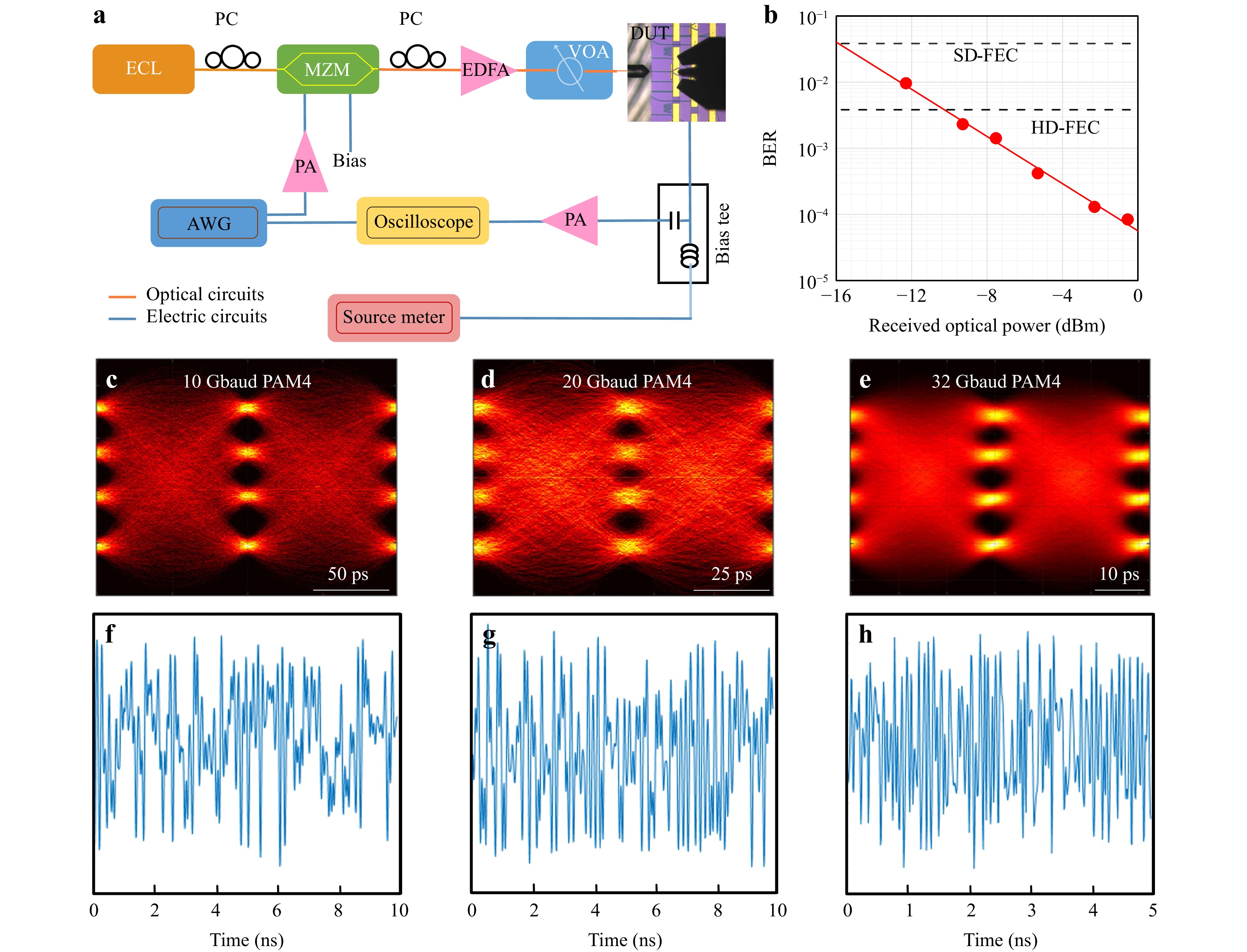
Fig. 8 a Intensity modulation and direct detection system setup. ECL: external cavity laser; PC: polarization controller; MZM: Mach-Zehnder modulator; EDFA: Erbium-doped fiber amplifier; DUT: device under test; AWG: arbitrary waveform generator. b Measured bit error rates (BERs) versus the received optical power for 32 Gbaud PAM4 signal. Eye diagrams c–e and measured waveforms f–h of the PAM4 signal with 10, 20, and 32 Gbaud.
-
This paper presents ultra-wideband waveguide-coupled MUTC photodiodes heterogeneously integrated on the thin-film lithium niobate platform. The bandwidths of the devices with active areas of 2 μm × 6 μm, 2 μm × 8 μm, 2 μm × 10 μm, 2 μm × 12 μm, and 2 μm × 14 μm were 110, 105, 100, 101, and 97 GHz, respectively. The bandwidth of the devices is limited by the transit time of the photo-generated carriers. The carrier transit time can be reduced by optimizing the thickness of the absorption layers and incorporating a diffusion block layer. Another factor limiting the device bandwidth is the large series resistance on p mesa. An InGaAs layer can be added as a p contact to reduce the contact resistance and thus, a larger RC-limited bandwidth. By following these practices, the device has the potential to boost the total bandwidth up to 200 GHz. The measured responsivities of the devices with lengths in the range of 6 – 14 μm were 0.4, 0.48, 0.5, 0.54, and 0.55 A/W. The intrinsic absorption of the metal stack sets the upper limit for the responsivity of the devices. An optimized, thicker cladding layer with a moderate doping level could mitigate the absorption of the metal stack and achieve higher responsivity. The devices were applied to a data transmission system, and the obtained results showed their ability to detect a 32 Gbaud PAM4 signal with high quality. It was demonstrated that the heterogeneously integrated photodiodes on TFLN platform have the potential to be applied in the next-generation high-speed transmission systems. This work paves the way to achieving massive-scale, multi-function, and high-performance TFLN photonic integrated circuits. Moreover, it holds a great promise for ultra-high-speed optical communications, high-performance integrated microwave photonics, and multi-function integrated quantum photonics.
-
The whole fabrication process of the heterogeneously integrated photodiode started from patterning LN waveguide and passive components by dry etching. A careful wet clean process was followed to ensure the cleanness of the TFLN wafer. Subsequently, a bare InP wafer was bonded onto the pre-patterned TFLN wafer. After wafer bonding, the InP substrate was mechanically thinned, followed by wet etching to remove the remaining part and expose the heavily doped InGaAs n-contact layer. N-mesa etch was performed to stop precisely at the InGaAsP p-contact layer by combining dry and selective wet etching. This step defined the size of the active region. The self-alignment method was applied in the fabrication process to ensure a precise alignment between the active region and the LN waveguide. P-mesa etching was performed using dry etching and selective wet etching to remove the InGaAsP above the LN wafer. To ensure the surface cleanness of the exposed LN wafer region, a wet chemical clean was performed. A 3-μm-thick SU-8 layer was deposited to form the base for the CPW pad. Metal electrodes with a GSG pad were formed by electroplating and lift-off. The wafer was finally diced into small chips, and the chips were then laterally polished.
-
In the frequency response test system (Fig. 6), a wavelength-tunable optical beat signal with 100% modulation depth was obtained using the heterodyne method, wherein the wavelength of one laser was fixed, while that of the other one was tuned. The polarization states of the two optical signals were controlled by two polarization controllers (PCs). An erbium-doped fiber amplifier (EDFA) and a variable optical attenuator (VOA) were used to adjust the optical power to the devices. The light was coupled into the waveguide through a lensed fiber with a spot size of 2.5 µm. The output RF signal of the photodiodes is accessed by the RF probe and transmitted to the power meter through the bias tee (SHF BT65R). The bias voltage was applied to the GSG pad through the bias tee.
For digital signal demodulation experiment, PAM4 signals with symbol rates of 10, 20, and 32 Gbaud were generated using the arbitrary waveform generator (AWG) with 25 GHz electrical bandwidth and 65 GSa/s sampling rate. The generated PAM4 signals were amplified by a power amplifier (SHF M827 B) and then applied to a 40 GHz Mach-Zehnder modulator (MZM). The output optical signal of the MZM was then amplified by an erbium-doped fiber amplifier (EDFA) and then detected by the fabricated device. The output RF signal of the device was amplified by a power amplifier (SHF M827 B) and sent to an oscilloscope with 33-GHz electrical bandwidth and 80-GSa/s sampling rate.
-
This work was supported by the National Key Research and Development Program (2022YFB2803800); Fundamental Research Funds for the Central Universities (2682022CX025).
Ultra-wideband Waveguide-coupled Photodiodes Heterogeneously Integrated on a Thin-film Lithium Niobate Platform
- Chao Wei1,
- Youren Yu1,
- Ziyun Wang1,
- Lin Jiang1,
- Zhongming Zeng2,
- Jia Ye1,
- Xihua Zou1,
- Wei Pan1,
-
Xiaojun Xie1, *, ,
 ,
, -
Lianshan Yan1, *, ,
- Light: Advanced Manufacturing 4, Article number: (2023)
- Received: 26 June 2023
- Revised: 17 August 2023
- Accepted: 24 August 2023 Published online: 12 September 2023
doi: https://doi.org/10.37188/lam.2023.030
Abstract: With the advantages of large electro-optical coefficient, wide transparency window, and strong optical confinement, thin-film lithium niobate (TFLN) technique has enabled the development of various high-performance optoelectronics devices, ranging from the ultra-wideband electro-optic modulators to the high-efficient quantum sources. However, the TFLN platform does not natively promise lasers and photodiodes. This study presents an InP/InGaAs modified uni-traveling carrier (MUTC) photodiodes heterogeneously integrated on the TFLN platform with a record-high 3-dB bandwidth of 110 GHz and a responsivity of 0.4 A/W at a 1,550-nm wavelength. It is implemented in a wafer-level TFLN-InP heterogeneous integration platform and is suitable for the large-scale, multi-function, and high-performance TFLN photonic integrated circuits.
Research Summary
Photodetection on Thin-film Lithium Niobate Platform: Ultra-wideband Heterogeneous Integrated Photodiodes
Thin-film lithium niobate (TFLN) technique has been widely adopted to develop various high-performance optoelectronics components due to its tight mode confinement and high nonlinear efficiency. However, TFLN platform, as a potential universal photonics integrated circuits (PICs) platform, faces the challenge that it lacks light source and photodetection natively. Xiaojun Xie and Lianshan Yan from Southwest Jiaotong University now report an ultra-wideband modified uni-traveling carrier photodiodes on the TFLN platform based on wafer-level heterogeneous integration technique. The fabricated device exhibited a 3-dB bandwidth of 110 GHz and a responsivity of 0.4 A/W at a wavelength of 1,550-nm wavelength. The device was applied to a data-receiving system and achieved an error-free reception of 32-Gbaud PAM4 signals. This work holds a great promise for massive-scale, multi-function, and high-performance TFLN photonic integrated circuits.
Rights and permissions
Open Access This article is licensed under a Creative Commons Attribution 4.0 International License, which permits use, sharing, adaptation, distribution and reproduction in any medium or format, as long as you give appropriate credit to the original author(s) and the source, provide a link to the Creative Commons license, and indicate if changes were made. The images or other third party material in this article are included in the article′s Creative Commons license, unless indicated otherwise in a credit line to the material. If material is not included in the article′s Creative Commons license and your intended use is not permitted by statutory regulation or exceeds the permitted use, you will need to obtain permission directly from the copyright holder. To view a copy of this license, visit http://creativecommons.org/licenses/by/4.0/.

 DownLoad: