


-
Scintillators that convert various types of high-energy radiation, including electromagnetic radiation and particle radiation, into ultraviolet-visible (UV-Vis) light have attracted extensive attention because of their broad application range in security inspection, nondestructive detection, medical imaging, and other fields1,2. Indirect detection using scintillators as the key components is a mainstream technology use for radiation detection3. Traditional commercial scintillators such as CsI:Tl4, Bi4Ge3O125, and (Lu, Y)2SiO56 have intense radioluminescence (RL); however, they still suffer from issues such as sluggish radiation transition dynamics, complex preparation processes, and high costs7,8. In recent years, self-trapped exciton (STE)-related lead-free metal halides have been studied extensively because of their high-emission efficiency, negligible self-absorption, lead-free characteristics, and flexible solution processibility9. However, the scintillation performance of all-inorganic lead-free halides remains to be addressed, especially in terms of spatial resolution and response time, compared with state-of-the-art scintillators. For instance, the photoluminescence (PL) lifetimes of Rb2CuCl3 and K2Cu(Cl, Br)3 are larger than 10 μs10,11, which limits their practical applications. Therefore, there is an urgent need to develop scintillators with comprehensive performance characteristics, such as high-emission efficiency and fast responses.
Hybrid organic–inorganic halides, which consist of large organic cations and isolated inorganic skeletons rich in heavy elements, have emerged as X-ray scintillators with excellent scintillation performance12,13. In terms of inorganic skeletons, low-dimensional hybrid cuprous halides can be broadly regarded as suitable candidates to replace the toxic lead ions (Pb2+) in the crystal structure with an eco-friendly cuprous ion (Cu+), which is desirable for scintillators with lead-free characteristics and self-absorption-free properties stemming from STE emission14,15. Regulating the composition, configuration, and size of organic ligands provides an opportunity to obtain excellent scintillation properties, including increased light-conversion efficiency, fast lifetime, and high-radiation stability16.
Compared with all-inorganic cuprous halides, the separation of the luminescent centers by the organic groups of hybrid cuprous halides enhances the confinement structure. This can promote the overlap of electron and hole wave functions, thus improving the photoluminescence quantum yield (PLQY) and scintillation response time. Furthermore, the fundamental bandgaps of these materials can be reduced by the rational chemical design of the organic ligands17. As is known, the light yield (LY, in photons per MeV) is one of the key parameters used to evaluate the scintillation performance, which can be expressed by the following equation: LY = (106/βEg)SQ, in which Eg represents the bandgap value (in eV), βEg represents the energy consumption for producing an electron-hole pair, and S and Q refer to the quantum efficiencies of transport and luminescence stage respectively18. According to this equation, a material with a low fundamental Eg value yields a high theoretical LY output, which is a precondition for achieving high-light yield scintillators. Based on our previous studies, we propose that the use of methyltriphenylphosphonium (MTP+) (which denotes [C19H18P]+) as the ligand is most likely to yield high-efficiency luminescent hybrid organic–inorganic cuprous halides. MTP+ was selected as the ligand because of its stable and bulky triphenyl structure, which may introduce a quantum confinement effect and endow the material with a high efficiency, fast emission, and short decay time. Large organic block groups provide enhanced stability and compatibility with the polymer matrix, making it easier to fabricate flexible composite films that match the geometry of complex objects.
In this study, zero-dimensional (0D) hybrid cuprous halide (MTP)2Cu4I6 single crystals (SCs) were synthesized and demonstrated an intense yellow emission peak at 618 nm with a large Stokes shift of 185 nm, a high PLQY of 99.9%, and a short fluorescence lifetime of 2.18 μs. Moreover, the (MTP)2Cu4I6 SCs achieved an LY of 43800 photons MeV−1 at an emission wavelength of 620 nm. In addition, the (MTP)2Cu4I6 SCs scintillators demonstrated superior detection performance with a good linear response ranging from 0.038 μGyair s−1 to 53.4 μGyair s−1 and a detection limit as low as 37.6 nGyair s−1. A flexible (MTP)2Cu4I6/polydimethylsiloxane (PDMS) composite scintillation film with dimensions of 30 mm × 30 mm × 1.0 mm was fabricated using a drop-coating approach. The high-spatial resolution was evaluated as 10.2 lp mm−1 when the modulation transfer function (MTF) is 0.2 for the flexible film, in which the planar and nonplanar X-ray imaging properties of a bent object were compared. Furthermore, (MTP)2Cu4I6 exhibits good stability under ambient conditions and X-ray irradiation.
-
High-quality (MTP)2Cu4I6 SCs were synthesized at 300 K using a facile antisolvent method, as shown in Fig. 1a. The detailed chemical synthesis route is described in the Materials and methods section. After a 24-h process, a batch of (MTP)2Cu4I6 SCs with a maximum length of 1.4 cm was successfully obtained. Needle-like yellow (MTP)2Cu4I6 SCs yielded intense yellow emission when exposed to 365 nm ultraviolet irradiation (Fig. 1b). The crystal structure and parameters of (MTP)2Cu4I6 were determined by SC X-ray diffraction (SC-XRD). It crystallizes in a monoclinic space group of R3c, with lattice parameters of a = 13.91 Å, b = 13.91 Å, c = 39.860 Å, α = 90°, β = 90°, γ = 120°, and V = 6680.9 Å3 belonging to the trigonal system (Table S1). Fig. 1c depicts a scheme of the (MTP)2Cu4I6 crystal structure in which purple octahedra correspond to [Cu4I6]2-, and orange and purple balls indicate I and Cu atoms, respectively. As shown, the photoactive sites, [Cu4I6]2- are isolated by MTP+ cations to form a 0D crystal structure (Fig. 1d). Large-volume cations favor the confinement effect, which increases the overlap of electron and hole wave functions and therefore promotes recombination19.
Fig. 1 a Schematic of the (MTP)2Cu4I6 crystal growth process. b Photograph of (MTP)2Cu4I6 crystals under natural light and 365 nm ultraviolet irradiation. c Crystal structure of (MTP)2Cu4I6. d Molecular structure of the MTP+ cation and configuration of the [Cu4I6]2− anion with normal thermal ellipsoids. e Experimental and theoretically calculated X-ray diffraction (XRD) patterns of (MTP)2Cu4I6.
The phase purity of (MTP)2Cu4I6 was confirmed using powder XRD. As shown in Fig. 1e, the measured intense diffraction peaks are consistent with the calculated results and can be attributed to the crystal planes of (MTP)2Cu4I6, indicating that (MTP)2Cu4I6 has a pure phase without secondary phase impurities. X-ray photoelectron spectroscopy (XPS) was used to investigate the elemental composition of the (MTP)2Cu4I6 (Fig. S1). Elemental XPS survey confirmed the presence of copper (Cu), iodine (I), and phosphorus (P) in the crystals (Fig. S1a). The peak correlated with Cu 2p can be well-fitted by the Gaussian equation, yielding a Cu 2p3/2 peak with a binding energy of 932.1 eV and a Cu 2p1/2 peak with a binding energy of 951.9 eV with a separation of 19.8 eV; these findings are consistent with the Cu+ ion (Fig. S1b)14,20. The XPS curves of I 3d contain the I 3d5/2 peak at 619 eV and the I 3d2/3 peak at 630.4 eV and have a separation of 11.4 eV; these findings are consistent with the I− ion (Fig. S1c)21. To evaluate the stoichiometry of (MTP)2Cu4I6, the quantitative composition of the high-resolution XPS spectra was examined (Table S2). The P: Cu: I molar ratio was 1.00: 2.08: 3.22, which is in good agreement with the stoichiometric value of (MTP)2Cu4I6. These results further indicate that the synthesized composition is consistent with the theoretical model.
To understand the electronic properties of (MTP)2Cu4I6, its band structure and density of states (DOS) were calculated using the density functional theory (DFT) calculations. As shown in Fig. 2a, the Cu orbitals contributed to the valence band, and the Cu and I orbitals contributed to the conduction band. The MTP+ cations have a negligible effect on the band edges, indicating a type-I band alignment (between the [Cu4I6]2− anions and the organic matrix) favored for efficient light emission22. The energy of the optical absorption onset resulting from excitonic absorption was 2.43 eV, as shown in the Tauc plot (Fig. S2). UV photoelectron spectroscopy (UPS) and inverse photoelectron spectroscopy (IPES) were performed on (MTP)2Cu4I6 to study the electronic properties of the sample surfaces. As shown in Fig. S3, the spectrum on the left side is the valence band from the UPS, whereas the spectrum on the right side is the conduction band from the IPES. For the (MTP)2Cu4I6, the valence band is evident and the valence band maximum (VBM) is −1.05 eV. The conduction band minimum (CBM) is 1.52 eV based on which an Eg of 2.57 eV is directly determined. This result is consistent with the optical bandgap obtained from the Tauc plot based on the absorption spectrum. Although the use of the generalized gradient approximation (GGA) method to calculate the bandgap typically tends to underestimate the value, this method can accurately determine the distribution of the electron DOS in both the conduction and valence bands. The DOS of Cu, I, C, and P elements with energy from −5 eV to 5 eV are shown in Fig. S4. The corresponding DOS of the elements Cu and I with energies from −1 eV to 1 eV are shown, indicating that the VBM of (MTP)2Cu4I6 consists of the antibonding states of Cu d orbitals, while the CBM is derived mainly from the bonding states of Cu s and I p orbitals (Fig. 2b, c). The s orbitals have a high degree of localization and large effective mass, leading to high-exciton binding energies, no collisions, and high-efficiency luminescence. The exciton binding energy (Eb) is usually calculated to evaluate exciton effects. The Eb of (MTP)2Cu4I6 is calculated to be 209.48 meV, according to the simplified Bethe–Salpeter equation Eb = μ*Ry/m0εr2, where μ* is the reduced exciton mass (μ* = me* × mh*/(me* + mh*)), Ry is the atomic Rydberg energy, and εr is the relative dielectric constant23. The calculation result also reveals that the εr is 4.69, and the me and mh values are 0.98 m0 and 16.48 m0, respectively.
Fig. 2 a Calculated band structure of (MTP)2Cu4I6. b Density of states (DOS) of Cu element. c DOS of I element.
PL and PL excitation (PLE) measurements were performed on the (MTP)2Cu4I6 crystals to explore their luminescence properties. As shown in Fig. 3a, the PL spectrum of (MTP)2Cu4I6 has a broad full-width-at-half-maximum (FWHM of ~209 nm) and a luminescence maximum of 618 nm with a sharp PLE peak at 456 nm. According to the DOS of (MTP)2Cu4I6 shown in Fig. 2b, the PLE spectrum can also be attributed to the charge transfer from the Cu s and I p orbitals (at the CBM) to the Cu d orbitals (at the VBM), and the intra-ionic transition of Cu+ ions. The UV-Vis absorption spectrum of (MTP)2Cu4I6 exhibited a single absorption peak at 433 nm below the band edge. In particular, the large Stokes shift of 185 nm (0.86 eV) indicates negligible self-absorption, which is characterized by a high-light-emitting efficiency. This large Stokes shift is attributed to the STE emission of (MTP)2Cu4I6. The self-trapping and relaxation processes of the excitons stimulated by the partial UV energy transfer to the lattice, resulted in a large energy difference and the generation of a large Stokes shift in the broadband emission. In addition, the emission of the (MTP)2Cu4I6 crystals possessed the Commission Internationale de l’Eclairage chromaticity coordinates of 0.474 and 0.501, which corresponded to yellow emission (Fig. S5). The PLQY of (MTP)2Cu4I6 was measured to be 99.9% using blank quartz as a reference; to the best of our knowledge, this is the highest PLQY reported to date for hybrid organic–inorganic metal halides (Fig. S6)13,24,25. Table S3 lists the PLQY of several previously reported cuprous halides. The high PLQY of (MTP)2Cu4I6 was attributed to both negligible self-absorption stemming from the large Stokes shift and the strong exciton restriction effect caused by the 0D structure26.
Fig. 3 a Ultraviolet-visible (UV-Vis) absorption, photoluminescence (PL), and PL excitation (PLE) spectra of (MTP)2Cu4I6. b Time-resolved PL spectra of (MTP)2Cu4I6. c Pseudo color map of the temperature-dependent PL spectra ranging from 260 K to 400 K of (MTP)2Cu4I6. d Integrated PL intensity as a function of the reciprocal temperature from 260 K to 400 K and the fitting curve of (MTP)2Cu4I6. e Temperature-dependent full-width-at-half-maximum and the fitting curve of (MTP)2Cu4I6. f Schematic of the self-trapped excitons (STE) luminescence of (MTP)2Cu4I6.
The photophysical properties of (MTP)2Cu4I6 SCs were characterized using time-resolved PL spectroscopy. The decay curve measured under 430 nm excitation at room temperature is shown in Fig. 3b and gives a single exponential PL lifetime of 2.18 μs. The short PL fluorescence lifetime contributes to a short afterglow of scintillators, which is a desirable property from the view of an ultrafast scintillation application. The several-microsecond lifetime of (MTP)2Cu4I6 is shorter than that of its all-inorganic counterparts. The well-fitted curves indicate that the exciton radiation composite channels are identical, verifying the presence of a single emitting center in the (MTP)2Cu4I6 crystal. The short PL lifetime is in line with those of cuprous halides including (Gua)3Cu2I5 (1.98 μs)27 and (TPA)CuI2 (5.25 μs)28, matching the decay time requirements of modern computed tomography (CT < 10 μs)29. The large Stokes shift and μs level fluorescence lifetime are consistent with the characteristics of STE emission30.
Temperature-dependent PL spectra were obtained to elucidate the underlying PL mechanism of (MTP)2Cu4I6 (Fig. 3c). The luminescence intensity gradually decreased as the temperature increased from 260 K to 400 K. In the cooling process, there was no emission peak splitting, which further verifies the presence of a single emitting center instead of multiple excited states in (MTP)2Cu4I6. Thermal quenching of the emission intensity was measured as a function of temperature to analyze the recombination process. The exciton activation energy (Ea) of (MTP)2Cu4I6 was obtained by fitting the Arrhenius formula (1)31 of the integrated PL intensity versus temperature:
$$ I(T) = \frac{{{I_{\text{0}}}}}{{1 + A\exp ( - {E_{\text{a}}}/{k_{\text{B}}}T)}} $$ (1) where Ea is the thermal activation energy, T is the test temperature, kB is the Boltzmann constant, and I0 is the integrated PL intensity at 0 K. As shown in Fig. 3d, the measured Ea of (MTP)2Cu4I6 is 322.9 meV, which is much higher than the thermal decomposition energy (26 meV) of binding excitons at 300 K and those of 3D perovskites32,33, which indicates that the exciton stability of (MTP)2Cu4I6 is high. High-exciton stability contributes to the thermal stability and high efficiency of fluorescence. The 0D crystal structure, and hence the low-electronic dimensionality and the confinement effect of the hybrid metal halides, contributes to the high Ea value.
The well-known Huang–Rhys factor (S factor) can be used to evaluate the formation tendency of STEs and can be derived from the temperature-dependent emission peak, which is obtained by fitting Eq. 234:
$$ {\text{FWHM}} = 2.36\sqrt S \hbar {\omega _{{\text{phonon}}}}\sqrt {\coth \left( {\frac{{\hbar {\omega _{{\text{phonon}}}}}}{{2{k_{\text{B}}}T}}} \right)} $$ (2) where FWHM is the full-width-at-half-maximum of PL spectra, S is the Huang–Rhys electron–phonon coupling parameter, $\hbar \omega $ is the phonon energy, kB is the Boltzmann constant, and T is the temperature. Fig. 3e shows that the S factor of (MTP)2Cu4I6 is 27.74, which is higher than the reported value for CsI (S = 12), indicating a strong electron–phonon coupling. This value presumably arises from the 0D structure and soft lattice of the material35, which tolerates more local polarization than the 3D structure of CsI. Thus, the stronger electron–phonon coupling in [Cu4I6]2− results in Jahn–Teller distortion and forms STEs36–38. The soft lattice and Jahn–Teller distortion of [Cu4I6]2− are the necessary conditions for the generation of STEs.
A configuration coordinate diagram was used to depict accurately STE formation and emission dynamics. As indicated by the vertical upward blue arrow, the ground state electrons transition to the excited state upon photoexcitation to form free carriers, which subsequently form free excitons with the release of exciton binding energy. During the formation of STEs, excited excitons and phonons undergo coupling interactions, internal conversion, and relaxation processes, which lead to lattice deformation and energy reduction. The STEs then transitioned back to the ground state, which was accompanied by radiation recombination and photon emission (Fig. 3f).
As the photoelectric effect (α∝ρZeff4 /E3) is the main interaction process of X-ray scintillation detection, the cross-sections for X-ray photons strongly depend on the atomic number of the X-ray scintillators26. The X-ray absorption coefficients of (MTP)2Cu4I6 and some conventional scintillators in the range of 0.001–100 MeV of photon energies according to the NIST XCOM photon cross-section database are shown in Fig. 4a. Owing to the composition of light atoms such as C, H, and P, the X-ray absorption coefficient of (MTP)2Cu4I6 is slightly lower than that of conventional scintillators such as CsI and LuAG:Ce. Nevertheless, (MTP)2Cu4I6 still has a satisfactory X-ray absorption capacity, which is higher than that of a representative organic scintillator, anthracene. Fig. S7 shows the absorption efficiency of (MTP)2Cu4I6, (MTP)2Cu4I6/PDMS (10% w/w), CsI, LuAG:Ce, and anthracene, as a function of thickness when the X-ray photon energy is 9 keV.
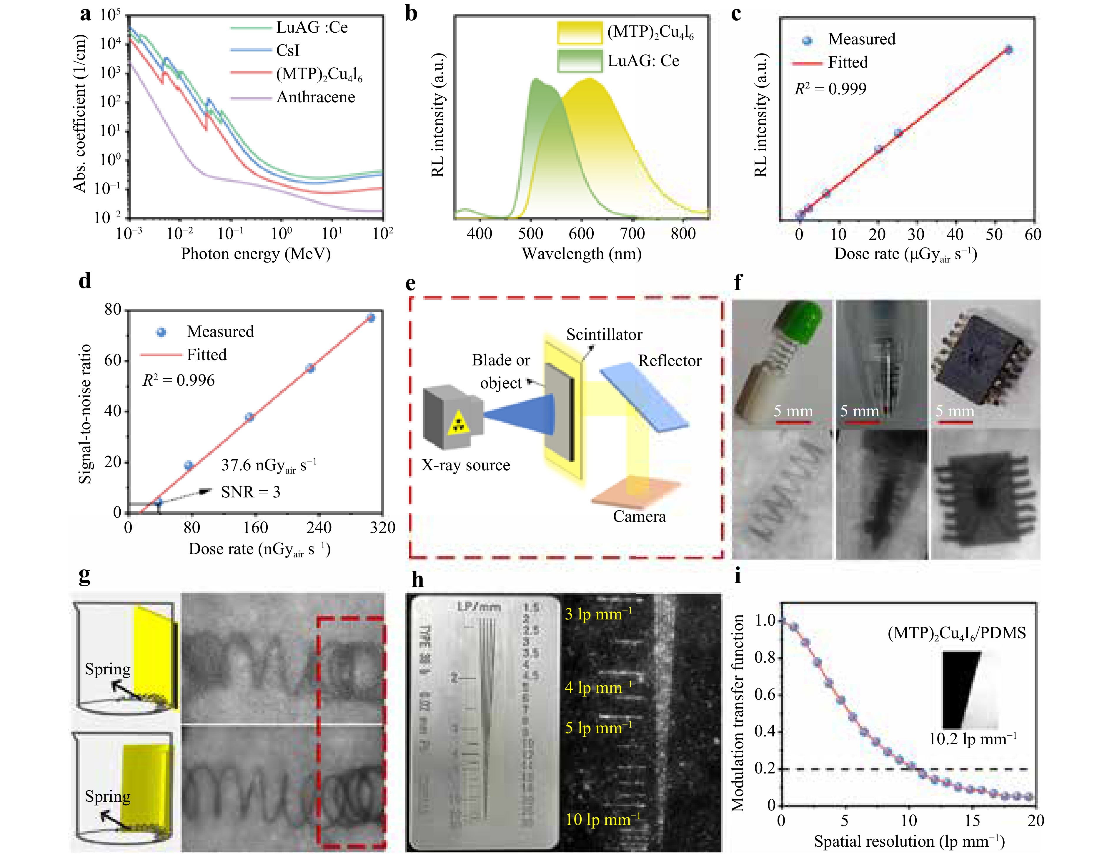
Fig. 4 a Absorption coefficients of (MTP)2Cu4I6, CsI, LuAG:Ce, and anthracene as a function of photon energy (from 1 keV to 100 MeV). b Radioluminescence (RL) spectra of (MTP)2Cu4I6 and LuAG:Ce under X-ray irradiation conditions. c Linear response of (MTP)2Cu4I6 covers a large range of four orders of magnitude from 0.038 μGyair s−1 to 53.4 μGyair s−1. d Signal-to-noise ratio (SNR) value versus the dose rates. e Illustration scheme of the X-ray imaging system. f Photographs under ambient light conditions and X-ray images of the objects including a metal spring encapsulated in a capsule, ballpoint pen, and a chip. g Schematic and X-ray images of a spring using planar and nonplanar (MTP)2Cu4I6/polydimethylsiloxane (PDMS) scintillator film adjacent to a beaker. h Photograph and X-ray image of a standard X-ray test-pattern plate. i Modulation transfer function (MTF) of the (MTP)2Cu4I6/PDMS composite film and the measured resolution (when the MTF value is 0.2). The inset shows the X-ray image of the tungsten edge used for MTF measurements.
To assess the scintillation properties, the RL spectrum of (MTP)2Cu4I6 was recorded under X-ray illumination conditions. As shown in Fig. 4b, the RL spectrum of (MTP)2Cu4I6 peaks at 620 nm, which is consistent with its PL spectrum, indicates that the PL process and the final stage of the scintillation process are similar39. In particular, a large Stokes shift is desirable for X-ray scintillators to avoid self-absorption because scintillators are very thick. Therefore, the benefit of the large Stokes shift in (MTP)2Cu4I6 is negligible self-absorption, thus achieving a high-light output efficiency, which has the potential to yield a high LY. An indirect approach was used to assess the X-ray scintillation LY of (MTP)2Cu4I6. The (MTP)2Cu4I6 SCs and reference scintillator LuAG:Ce with a reported LY value of 25000 photons MeV-1 were individually placed in an integrating sphere at a fixed distance from the X-ray source to unify the radiation dose and field. Compared with LuAG:Ce, the (MTP)2Cu4I6 SCs exhibited a much higher RL intensity with a broader linewidth. Comparing the fluorescence integral areas, the calculated LY of (MTP)2Cu4I6 was approximately 1.75 times that of LuAG:Ce. As a result, the LY of (MTP)2Cu4I6 was estimated to be 43800 photons MeV−1, which is comparable to that of reported cuprous halide scintillators (Table S3). The effective STE emission, quantum confinement effect, low bandgap, and high-crystal quality, are responsible for the high LY values.
To assess the linear response of the (MTP)2Cu4I6 scintillator for applications at different radiation dosages, the RL spectra of (MTP)2Cu4I6 were measured at different X-ray dose rates (Fig. S8). The (MTP)2Cu4I6 exhibited a good linear response (over four orders of magnitude) with X-ray dose rates ranging from 0.038 μGyair s−1 to 53.4 μGyair s−1 (Fig. 4c). The detection limit derived from the fitting curve in Fig. 4d is 37.6 nGyair s−1 when the SNR is 3, which was comparable with the reported cuprous halide scintillators (Table S3) and much lower than the 5.5 μGyair s−1 required for medical diagnoses40.
PDMS was selected as the matrix because of its high-radiation hardness, optical transparency, flexibility, and low-absorption coefficient in the visible-light range41. The (MTP)2Cu4I6/PDMS flexible scintillator film was prepared by dispersing ground (MTP)2Cu4I6 SCs powders in PDMS. Consequently, a large-sized (MTP)2Cu4I6/PDMS flexible scintillator film with dimensions of 30 mm × 30 mm × 1.0 mm was obtained. Photographs of (MTP)2Cu4I6 under natural light and UV excitation conditions can be found in Fig. S9. The favorable transparency of the scintillation film enables the pattern to be visible under natural light and UV excitation conditions. The UV-Vis absorption spectrum of the (MTP)2Cu4I6/PDMS composite film is shown in Fig. S10.
To verify the imaging ability of the large-area and intense X-ray-excited luminescent (MTP)2Cu4I6/PDMS composite film, we conducted an imaging experiment using a custom-made X-ray imaging system (Fig. 4e). A reflector is commonly used in scintillation detection systems to prevent the detection of electronics from risking X-ray radiation damage and to improve the field of view. Three different objects were placed between the X-ray source and (MTP)2Cu4I6/PDMS composite film to conduct a proof-of-concept experiment. The metal springs inside the opaque capsule, tip of the ballpoint pen, and the metal inside the internal circuitry of the chip were directly visualized without blurring (Fig. 4f). These results demonstrate the potential of the (MTP)2Cu4I6/PDMS composite film organic molecules as X-ray scintillator screens for radiography applications.
Because the (MTP)2Cu4I6/PDMS scintillator film had good flexibility, as shown in Fig. S11, a comparative experiment of planar and nonplanar X-ray imaging was performed according to the schematic in Fig. 4g. Similar to a traditional planar X-ray imaging setup, the scintillator film was placed behind a nonplanar object. As shown, the image of the bent spring exhibited distortion at the bend edges when planar X-ray imaging was used. When applied to non-planar X-ray imaging, a flexible scintillator film can be bent according to the curvature of the object and tightly attached to it. Thus, the spring was imaged more clearly by the nonplanar scintillator film, especially the bent edges of the spring, as indicated by the dashed-boxed region in the image. Notably, the bent edges of the spring are more clearly observed on the flexible detector than on its planar counterpart. Therefore, the exceptional flexibility of the flexible (MTP)2Cu4I6/PDMS scintillator film enables the clear curved surface imaging of nonplanar objects. Considering its excellent X-ray imaging abilities, the (MTP)2Cu4I6/PDMS scintillator film is a potential candidate for low-dose flexible X-ray detectors.
X-ray imaging of the standard test-pattern plate in Fig. 4h demonstrated that a spatial resolution greater than 10 lp mm−1 was clearly distinguished in the image. A tungsten plate was tilted at a certain angle to obtain X-ray images and quantify the spatial resolution (Fig. S12, 4i). The spatial resolution was determined to be 10.2 lp mm−1 when the MTF was 0.2, further confirming the high-spatial resolution of the (MTP)2Cu4I6/PDMS film. The spatial resolution of the (MTP)2Cu4I6/PDMS film is comparable to those of several previously reported metal halide scintillators (Table S4). Decreasing the thickness of the scintillator film can help improve the spatial resolution of X-ray imaging; however, a larger dose rate is always required to produce a sufficient scintillating light signal in practical X-ray imaging. Future improvements can be made by optimizing the balance between light scattering, light output, and thickness-dependent cross sections of X-rays.
Hybrid metal halides with natural confinement structures typically exhibit excellent stability. Accordingly, the thermal stability of the (MTP)2Cu4I6 scintillator, which is vital for practical applications, was investigated. Fig. S13 shows the thermogravimetric analysis (TGA) and differential scanning calorimetry (DSC) curves of (MTP)2Cu4I6. As shown, the TGA results demonstrate a negligible weight loss at 673 K, indicating the high thermal stability of (MTP)2Cu4I6. The melting point of (MTP)2Cu4I6 occurred at 403 K where there was an endothermic peak without mass loss. When the temperature exceeded the weight loss onset temperature at 684 K, two decomposition processes were likely to occur: 1) (MTP)2Cu4I6 → 2(MTP)I + 4CuI (at 763 K), and 2) decomposition of CuI (at 891 K)42. In addition, owing to the lattice stability provided by the organic cations, the (MTP)2Cu4I6 scintillator exhibited degradation-free XRD patterns and PL emission after storage in air for 60 d and under continuous X-ray irradiation conditions (Fig. 5). As shown in Fig. 5a, c, the crystal structure and PL intensity displays insignificant changes even after 60 d, suggesting long-term stability. As shown in Fig. 5b, d, after continuous ionization at a total dose of 789 mGyair, the XRD patterns become identical, and the PL intensity decreased to approximately 90% of its original value. Finally, the scintillation performance of the (MTP)2Cu4I6 composite films was tested using repeated X-ray irradiation to evaluate their photostability. As shown in Fig. S14, the emission intensity of the (MTP)2Cu4I6/PDMS film was stable even under cyclical X-ray excitation with a dose of 100 mGyair s−1, revealing high X-ray radiation resistance of (MTP)2Cu4I6 for scintillation applications.
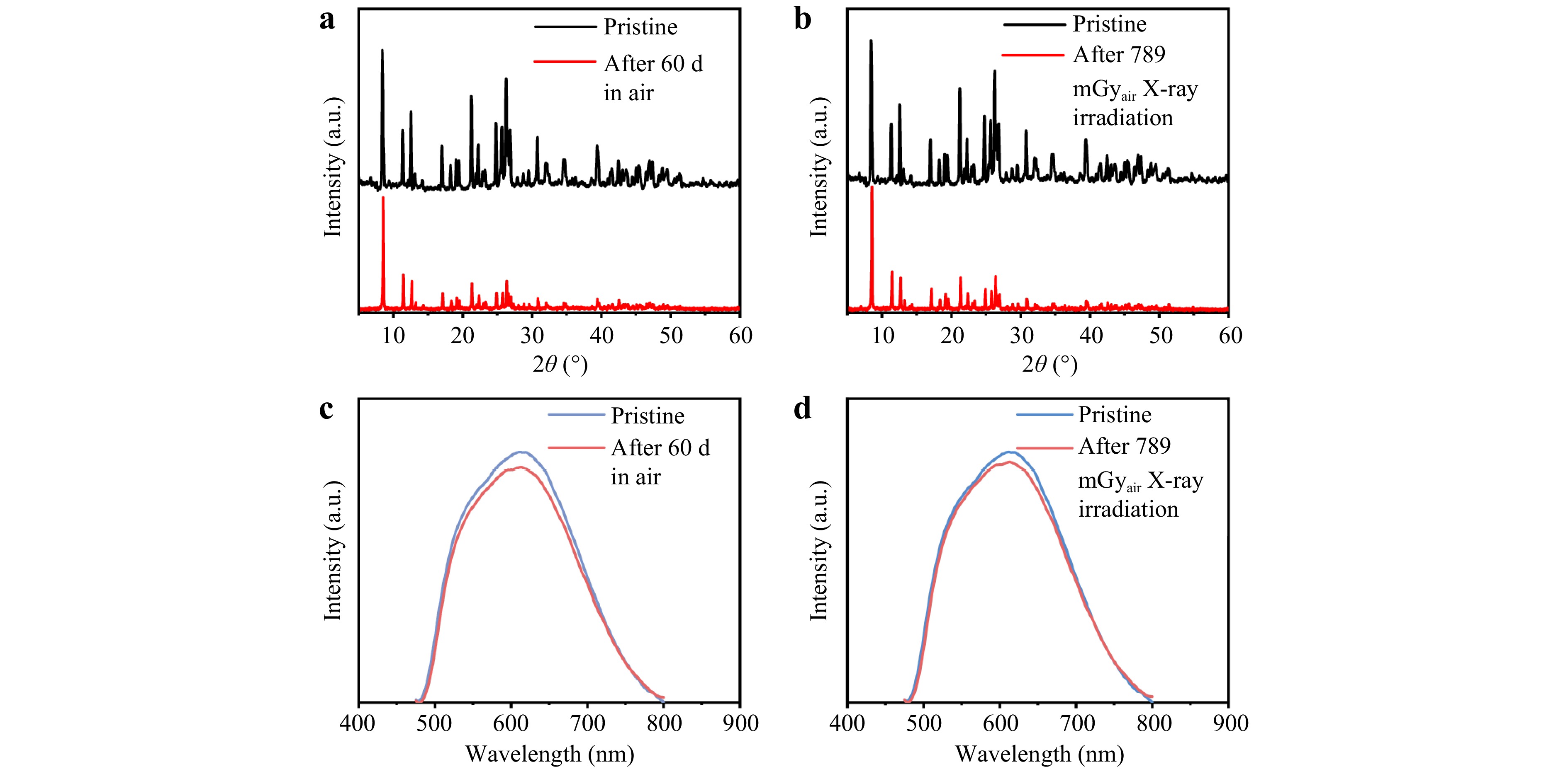
Fig. 5 a XRD patterns of pristine and (MTP)2Cu4I6 after 60 d of ambient storage. b XRD patterns of pristine and (MTP)2Cu4I6 after a total X-ray irradiation of 789 mGyair. c PL spectra of pristine and (MTP)2Cu4I6 after 60 d of ambient storage. d PL spectra of pristine and (MTP)2Cu4I6 after a total X-ray irradiation of 789 mGyair.
Although (MTP)2Cu4I6 has the aforementioned merits, some potential problems exist, especially in practical applications. Organic groups are known to a decrease the absorption coefficient of the material for X-rays. A generalized method used to solve this problem is to thicken the scintillation layer to achieve excellent detection properties, which, in turn cause a significant increase in pixel crosstalk of the photodetector matrix. Scattering by the matrix became particularly pronounced as the thickness of the membranes increased. The scattering problem in bulk CsI:Tl crystals can be resolved by fabricating pixelated scintillator arrays. A pixelated CsI:Tl scintillator array can be prepared using a pixelated matrix or vacuum thermal evaporation to grow CsI:Tl crystals with columnar structure43,44. The pixelated CsI:Tl scintillator array endows CsI:Tl with a higher light extraction efficiency than that of the bulk scintillator array. Similarly, a pixelated scintillator composite screen can be obtained by embedding the (MTP)2Cu4I6 scintillators into a pixelated template. In addition, (MTP)2Cu4I6 array scintillators can be prepared with an ordered arrangement of needle-like (MTP)2Cu4I6 crystals. In addition, the optical transparency of the film is a key factor in the light-extraction efficiency of scintillators, which is crucial for achieving high resolution. Owing to the inevitable scattering by the scintillator particles in the film, the optical transparency of the composite films was lower than those of the SCs. Optimized scintillator loading and uniformity can reduce scattering and improve the transparency of composite films. Therefore, future improvements can be achieved by optimizing the balance between light scattering, loading, and the thickness-dependent X-rays cross-sections.
-
In summary, we designed a 0D hybrid cuprous halide (MTP)2Cu4I6 and successfully prepared SCs using a solution method. This material showed intense yellow STE emission with negligible self-absorption and high PLQY outputs (up to 99.9%). The (MTP)2Cu4I6 scintillator showed strong RL and superior X-ray scintillation properties and yielded a high LY value (approximately 43800 photons MeV−1), good linear scintillation response range, and a low-detection limit. Moreover, the (MTP)2Cu4I6 SCs exhibited excellent thermal, atmospheric, and irradiation stabilities. In addition, an (MTP)2Cu4I6 scintillator was fabricated as a flexible (MTP)2Cu4I6/PDMS film with a large area of up to 9.0 cm2. The radiography prototype demonstrates a high-quality imaging ability that yields high-contrast X-ray images of objects and realizes a high-spatial resolution of 10.2 lp mm−1. This study demonstrates the potential applications of new cuprous halide scintillators for flexible X-ray imaging.
-
Materials: Cuprous iodine (CuI) (Adamas-Beta, 99%), methyltriphenylphosphonium iodide ((MTP)I) (Adamas-Beta, 98%), hydroiodic acid (HI) (Adamas-Beta, 55-57 wt.% solution in water), hypophosphorous acid (H3PO2) (Adamas-Beta, 50 wt.% solution in water), ethanol (EtOH) (Aladdin, 99%). The above materials were purchased from Shanghai Titan Technology Co. Ltd. Acetonitrile (ACN) (J&K Scientific, 99%) was purchased from Beijing J&K Scientific Reagent Co. Ltd. PDMS was purchased from Dow Chemical Company. All chemical materials and solvents were of reagent grade and used without further purification.
Synthesis of (MTP)2Cu4I6: The (MTP)2Cu4I6 SC was synthesized using the antisolvent method at 300 K. Specifically, 3.15 mmol cuprous iodide and 1.48 mmol methyltriphenylphosphonium iodide were dissolved in mixed solvents of 4 mL acetonitrile, 1 mL hydrogen iodide, and 100 μL hypophosphorous acid (to prevent oxidation of Cu+). The mixture was heated under 353 K for approximately 30 min to make it evenly dissolved. The solution was then filtered by a 0.22 μm filter membrane to remove impurities. The clear orange solution was then added to 15 mL of anhydrous ethanol, which finally became stratified. The vials were sealed to prevent external contamination and incubated at room temperature. After 24 h, (MTP)2Cu4I6 precipitated in the form of needlelike yellow crystals. The crystallized samples were washed with anhydrous ethanol and air dried. Subsequent characterizations of the crystal properties and testing of the detection properties were performed using the as-prepared SCs.
Fabrication of (MTP)2Cu4I6/PDMS film: First, the (MTP)2Cu4I6 crystals were ground in an agate mortar for 30 min to obtain powders. PDMS was then prepared by mixing the prepolymer with the curing agent in a mass ratio of 10:1. The ground (MTP)2Cu4I6 crystal powder and PDMS were mixed with a scintillator loading of 10% (w/w) and continuously stirred for 1 h to form a colloidal solution. Finally, the colloidal solution was dropped in a mold, vacuumed at room temperature for approximately 30 min to remove bubbles, and heated at 353 K for 3 h to form a flexible film.
Characterization: SC-XRD was measured using a Bruker D8 Venture X-ray diffractometer with Cu Kα radiation (λ = 1.5418 Å). Powder X-ray diffraction patterns were characterized using a Bruker D8 Advance X-ray diffractometer with Cu Kα radiation (λ = 1.5418 Å). The calculated powder diffraction patterns were obtained using the VESTA software program. XPS was performed on a Shimadzu AXIS Supra+ instrument with data analysis using the Avantage software program. TGA was performed using a Netzsch STA 449 F5 thermal analyzer in the temperature range of 303–1073 K under Argon atmosphere conditions. UV-Vis absorption spectra were obtained using a Hitachi UH4150 UV-Vis spectrophotometer in the wavelength range of 250–800 nm in steps of 1 nm. The PL and PLE spectra were obtained using an Edinburgh FLS1000 fluorescence spectrometer with a xenon lamp as the excitation source. Time-resolved PL were performed using an Edinburgh FLS1000 fluorescence spectrometer equipped with a laser. The average lifetime was obtained using exponential fitting. PLQY was determined by incorporating an integrating sphere into a Hamamatsu C9920-02G spectrofluorometer. The temperature-dependent PL emission spectra were recorded using an Edinburgh FLS1000 fluorescence spectrometer. The UPS and IPES spectra were measured using an ESCALAB QXi instrument.
RL spectroscopy and LY measurements: The RL spectra were collected using a MOXTEK MAGPRO TUB00154-9I-06 X-ray tube. LuAG:Ce with a known LY of 25000 photons MeV−1 was used for the reference scintillator to estimate the LY of (MTP)2Cu4I6 SC. Both were standardized to the same dimensions. The (MTP)2Cu4I6 SC and LuAG:Ce reference scintillators were placed in the same position as the X-ray source to acquire the RL spectra. To calculate LY, the X-ray absorption efficiency (AE) was first calculated using Eq. 3:
$$ {\text{AE}}\left( {\text{%}} \right) = \left( {1 - {e^{{\mu _{\text{L}}}{\text{t}}}}} \right) \times 100{\text{%}} $$ (3) where μL is the linear attenuation coefficient, and t is the thickness. The X-ray AEs of the (MTP)2Cu4I6 SC and LuAG:Ce are shown in Fig. S7, and were calculated to be 0.999 and 1 at a thickness of 1 mm, respectively. The measured integrated counts (ICs) of the RL spectra were individually normalized for LY calibration using Eq. 4:
$$ {\text{I}}{{\text{C}}_{{\text{normalized}}}} = \frac{{{\text{I}}{{\text{C}}_{{\text{measured}}}}}}{{{\text{AE}}\left( {\text{%}} \right)}} $$ (4) The LY of the sample can be calculated using Eq. 5:
$$ \frac{{{\text{L}}{{\text{Y}}_{{\text{sample}}}}}}{{{\text{L}}{{\text{Y}}_{{\text{LuAG:Ce}}}}}} = \frac{{{\text{I}}{{\text{C}}_{{\text{normalized}}}}\left( {{\text{sample}}} \right)}}{{{\text{I}}{{\text{C}}_{{\text{normalized}}}}\left( {{\text{LuAG:Ce}}} \right)}} $$ (5) X-ray imaging: We used at TUCSEN Cooled B&W complementary metal-oxide semiconductor (CMOS) camera FL 20BW to capture photographs of the X-ray-excited luminescence. The equipment was placed in a lead box. The images were captured by a CMOS camera under an X-ray tube operated at 50 kV and 200 μA with different exposure times.
DFT calculations: The (MTP)2Cu4I6 model was constructed according to XRD analysis. Both geometric structural optimization and electronic structure calculations were performed based on first-principles calculations. VASP code was employed in conjunction with the projector-augmented wave method45. The exchange-correction interaction is described by the Perdew (Burke) Ernzerhof functional according to the GGA46. The van der Waals interactions were corrected using the Grimme D2 method47. The cutoff energy was set at 400 eV. The convergence criteria for total energy and residual atomic forces were 10−5 eV/atom and 0.01 eV/Å, respectively. The Monkhorst–Pack k-point mesh in the Brillouin zone was set to be Γ-centered with a k-spacing of ~0.015 Å−1.
-
This work was financially supported by the National Natural Science Foundation of China (62374128), Guangdong Basic and Applied Basic Research Fund (2023A1515030084), and the Key Research and Development Program of Shaanxi Province (Grant 2024GX-YBXM-512). This research was also supported by the Open Project Program of Wuhan National Laboratory for Optoelectronics (2022WNLOKF004), Qin Chuangyuan Innovation and Entrepreneurship Project (QCYRCXM-2022-316), Fundamental Research Funds for the Central Universities, and the Fund of Innovation Centre for Radiation Application (KFZC2023020902); it was also supported by the Fund of the State Key Laboratory of Solidification Processing in NPU (SKLSP202406), Postdoctoral Fellowship Program of CPSF under Grant Number (GZB20230673), and by the Key Research Projects of Higher Education Institutions in Henan Province (24A140020).
Large-area, high-resolution, flexible x-ray scintillator film based on a novel 0d hybrid cuprous halide
- Light: Advanced Manufacturing , Article number: (2025)
- Received: 11 June 2024
- Revised: 24 April 2025
- Accepted: 29 April 2025 Published online: 30 October 2025
doi: https://doi.org/10.37188/lam.2025.044
Abstract: X-ray scintillation detectors play an irreplaceable role in medical imaging, security inspections, and nondestructive detection. Recently, all-inorganic lead-free metal halide scintillators have attracted attention for addressing the drawbacks of lead-halide perovskites, such as severe self-absorption and toxicity. Nevertheless, high-resolution, flexible, and cost-effective lead-free scintillators are desirable for X-ray imaging applications. In this study, we designed a zero-dimensional hybrid cuprous halide, (MTP)2Cu4I6 (MTP+ represents [C19H18P]+), and synthesized single crystals. (MTP)2Cu4I6 shows intense yellow emission (618 nm) and a large Stokes shift of 185 nm, almost eliminating the effect of self-absorption. As a result, (MTP)2Cu4I6 exhibited a near-unity photoluminescence quantum yield (99.9%) with a light yield of 43800 photons per megaelectron volt. Moreover, (MTP)2Cu4I6 demonstrates an impressive detection performance with a fast response time of 2.18 μs, a good linear response ranging from 0.038 μGyair s−1 to 53.4 μGyair s−1, and a low detection limit of 37.6 nGyair s−1. In a conceptual experiment, large-area flexible (MTP)2Cu4I6/polydimethylsiloxane (PDMS) scintillation films were fabricated to investigate their X-ray imaging performance. The (MTP)2Cu4I6/PDMS film exhibits a high-spatial resolution of 10.2 lp mm−1 when the modulation transfer function is 0.2 and superior flexible detection performance. The short lifetime, high-light yield, low toxicity, and low cost of (MTP)2Cu4I6 facilitate the development of next-generation X-ray scintillators.
Research Summary
X-ray scintillators: A flexible, lead-free alternative for high-resolution imaging
A lead-free scintillator single crystal that achieves high-resolution X-ray imaging shows potential in high performance X-ray detection and flexible detectors fabrication. X-ray scintillation detectors are vital for medical imaging and security inspection, yet lead-free, high-performance alternatives to toxic lead-halide perovskites are needed for X-ray imaging. Jingjing Chang’ group from China’s Xidian University reports a novel zero-dimensional hybrid cuprous halide scintillator, (MTP)₂Cu₄I₆, (MTP+ = [C19H18P]+), which exhibits intense yellow emission with a near-unity photoluminescence quantum yield. The material demonstrates exceptional detection performance, including a fast response time, a broad linear response, and an ultra-low detection limit. Flexible films achieve special resolution as high as 10.2 lp mm-1 which sustain the excellent X-ray imaging property under bending. With low-toxicity and cost-effectiveness, this material surely fosters the development of next-generation X-ray scintillators and improves medical and security imaging.
Rights and permissions
Open Access This article is licensed under a Creative Commons Attribution 4.0 International License, which permits use, sharing, adaptation, distribution and reproduction in any medium or format, as long as you give appropriate credit to the original author(s) and the source, provide a link to the Creative Commons license, and indicate if changes were made. The images or other third party material in this article are included in the article′s Creative Commons license, unless indicated otherwise in a credit line to the material. If material is not included in the article′s Creative Commons license and your intended use is not permitted by statutory regulation or exceeds the permitted use, you will need to obtain permission directly from the copyright holder. To view a copy of this license, visit http://creativecommons.org/licenses/by/4.0/.

 DownLoad: