





-
Micro-light-emitting diodes (micro-LED) are widely recognized as the most promising technology for the next-generation display industry, especially for augmented/virtual reality (AR/VR) head-mounted displays (HMDs), also known as near-eye displays. Contemporary near-eye displays demand stringent performance metrics, including ultrahigh resolution, high refresh rates, exceptional brightness, high contrast ratios, and robust environmental reliability1–19. GaN-based micro-LEDs exhibit super efficiency, reliability, and brightness in the blue and green spectral region compared to quantum dot micro-LEDs, and hold great potential to replace AlGaInP red micro-LEDs owing to their milder efficiency degradation for ultra-small pixels20–22.
Micro-LED displays on CMOS backplanes have been extensively investigated over the past decades23–31. Flip-chip bonding, the most prevalent method for integrating micro-LED pixels onto CMOS backplanes via metal bumps (e.g., Au-Au, Au-Sn, or In-In), has been widely utilized32 to realize high-resolution, high-PPI micro-displays for AR/VR applications. However, flip-chip bonding requires exceptional precision in solder bump dimensional tolerances, topographical uniformity, and sub-micron alignment accuracy for high pixel density (HPD) display. While the horizontal configuration of flip-chip bonded micro-LED reduces the effective lighting area due to non-emissive peripheral regions occupied by n-GaN cathode electrodes33, hindering pixel density scaling within a given display area. In contrast, the wafer bonding method directly bonds the micro-LED epi-wafer to the CMOS wafer before pixelation, enabling the vertical configuration of micro-LED to be defined from the wafer's backside. The size of micro-LED pixels is determined by the precision of photolithography, which facilitates higher pixel density. To date, the largest reported size of micro-LED micro-displays is 0.69 inches34, the maximum reported PPI of such displays is 6,77335. In the current micro-display landscape, there is a notable inverse correlation between pixel density and panel size23–31. This trade-off creates a significant barrier for applications that require both high resolution and an expanded active area. Although wafer bonding can address these technical bottlenecks to enable micro-LED displays with higher PPI, it still faces challenges such as pixel defects or uneven brightness, which are typically caused by the combined effects of driving substrate performance, driving algorithms, and chip manufacturing processes. Broadly speaking, current micro-LED technology still remains immature in terms of epitaxial materials, fabrication processes, and driving circuitry. There are very few reports on the brightness uniformity of micro-LED displays, a critical parameter for their practical deployment in commercial applications.
In this work, we demonstrate the heterogeneous integration of green micro-LED with Si CMOS backplanes using a wafer-bonding approach. The resulting display array features a high resolution of 1,472 × 1,104 pixels (1,814 PPI) with a 14 µm pixel pitch. To realize high brightness and emission uniformity across the entire display screens, we combined a high-consistency pixel driver design with a robust fabrication process specifically optimized to mitigate wafer bowing, surface planarity, and backside etching damage. Circuit simulations verify the precision of this approach, showing exceptional current consistency (Monte Carlo 3σ/μ=0.2%) and linearity (DNL/INL <0.004 LSB). Consequently, the display achieves a peak luminance exceeding 20,000 cd·m−2 with 90% uniformity at 0.5 A·cm−2, while maintaining a wide viewing angle (>120°) and 8-bit grayscale capability. These results validate the scalability of our heterogeneous integration approach, highlighting its potential for industrial-scale manufacturing of next-generation near-eye display systems.
-
The CMOS backplane was custom-designed to control the brightness of each pixel within the display screen by outputting precise currents. Fig. 1a presents the driver architecture of high-resolution micro-displays which employs a hybrid architecture combining on-chip and external driving systems. The on-chip driver employs a digital pulse-width modulation (PWM) scheme, integrating a pixel array, direct current to direct current (DC-DC) converters, a low dropout regulator (LDO), an inter-integrated circuit (I2C) interface, temperature sensors, and a high-speed low voltage differential signaling (LVDS) interface. In this design, pixel illumination duration within a single frame is dynamically adjusted by digital PWM scanning according to grayscale data, mitigating luminance discontinuities arising from the nonlinearity of the current-luminance characteristic of micro-LED. Notably, unlike analog driving methods requiring continuous voltage modulation, the digital approach utilizes two discrete voltage levels (maximum and minimum current) selected from the steep current-voltage (I-V) curve of micro-LED. This strategy effectively eliminates grayscale inaccuracies inherent to analog modulation while improving display uniformity. Grayscale modulation is accomplished within 8 subframes, where each subframe adopts a rolling shutter scanning method. Each row is sequentially scanned with binary-weighted pulses. The driver system processes display data through the following stages: first, the data is converted into an appropriate format and stored in the data random-access memory (RAM), then, a subspace scanning module generates synchronized subspace codes, weight codes, and blanking codes. The pixel matrix address decoder produces corresponding row/column addresses based on these subspace codes, and the addresses are then transmitted to the pixel matrix decoding circuitry. Simultaneously, the RAM controller extracts target display data via address-weight code pairs and transfers it to the pixel matrix data latches, completing the frame rendering cycle. The insets in Fig. 1b illustrate the circuit and layout of the pixel, which is based on static random-access memory (SRAM) and maintains bistable '0'/'1' states with low leakage. The simulated results in Fig. 1b demonstrate a good linearity between grayscale (0−255) and average pixel current across the full brightness range when adjusted by PWM. Both differential non-linearity (DNL) and integral non-linearity (INL) are below 0.004 LSB across all grayscales in Fig. 1c, indicating exceptional sub-LSB current precision to enable accurate grayscale control (8-bit grayscale), a linear response for low-grayscale fidelity, and robust circuit design that mitigates process variations (e.g., transistor mismatch). Monte Carlo simulations of 200 pixels (Fig. 1d) show a standard deviation (σ) of 687 pA at a mean pixel current (μ) of 1 μA. The ratio of three times standard deviation to mean (3σ/μ) reveals that 99.7% of pixel currents are within ±0.2% of the mean value, demonstrating excellent pixel current consistency. The pixel current deviation across the whole active area is less than 10% at a full-screen current of 0.5 A (Fig. 1e), indicating good brightness uniformity across the whole display screen.
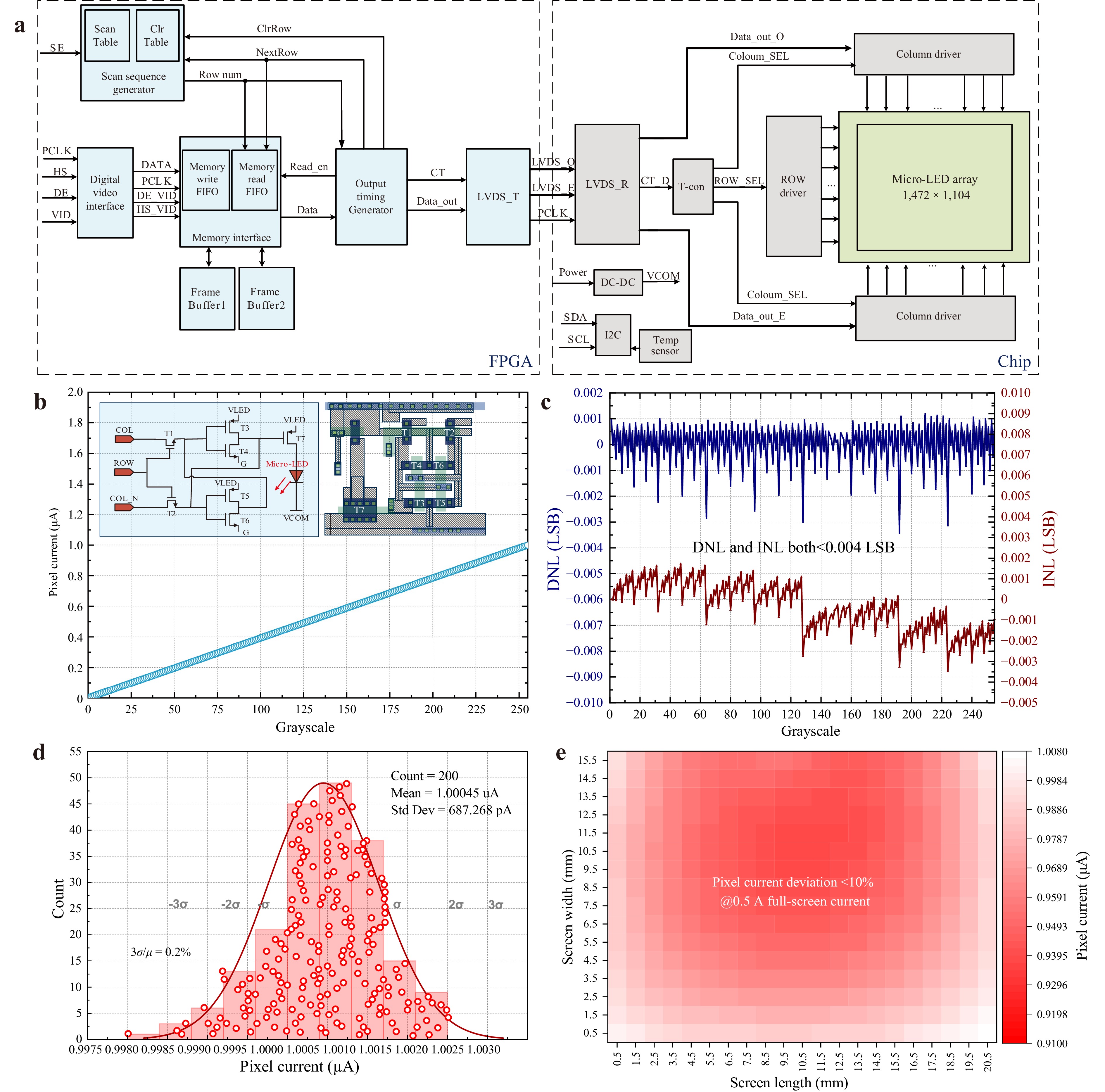
Fig. 1 Design of driver and simulations of CMOS driving capabilities. a Driving circuit architecture of the high-resolution micro-LED displays with grayscale generation via PWM method. b SRAM-based pixel circuit and layout with output current linearly varying over 0−255 grayscale levels. c DNL and INL simulation based on an individual pixel at 1 µA, both less than 0.004 LSB, indicating excellent linearity of the current. d Monte Carlo simulation for pixel current uniformity with standard deviation (σ) of 687 pA at a mean pixel current (μ) of 1 μA, indicating excellent pixel-level consistency of the current output without mura. e Simulation of pixel array currents across different regions on the CMOS backplane with uniformity greater than 90%.
-
The heterogeneous integration of the fabricated GaN-based green micro-LED array on a custom Si CMOS platform is achieved by wafer bonding scheme. From a process perspective, the primary objective is to minimize pixel-level imperfections, such as leakage current and defects, through precise measurement and optimized control at each manufacturing step. The optimized key parameters for wafer bonding (temperature: 280 °C, pressure: 8,000 kgf) are adopted, which effectively alleviates interfacial stress and thermal mismatch (Inferior data can be found in Fig. S2 and Fig. S3 in Supplementary information). This effort ultimately supports the achievement of high brightness and superior uniformity in micro-LED micro-displays, with the pixel yield reaching 93.24%. Detailed estimation can be found in Fig. S1 in Supplementary information.
Fig. 2a shows the fabrication schematic of the micro-LED display screen. Fig. 2b depicts the layout of the micro-LED display, involving micro-LED arrays (1,472 × 1,104), pixel circuit arrays, and peripheral circuits. First, a layer of 100 nm thick indium tin oxide (ITO) was deposited on the surface of p-GaN as a current spreading layer by electron beam evaporator (EBE) and annealed to form good p-type ohmic contact. A total thickness of 500 nm Au-Sn metal is deposited on the surface of the p-GaN layer and the interconnect pads of the CMOS panel, respectively. Then the 4-inch LED wafer and the CMOS backplane were well bonded. The low bonding void ratio, indicating uniform interfacial adhesion and high-quality bonding integrity, is confirmed through the scanning acoustic microscopy (SAM) image in Fig. 2c, where the white bubbles represent the bonding voids. This high-quality wafer bonding can be attributed to the low bow values (typically <50 μm) and few surface particles for both 4-inch LED wafer and CMOS backplane. After examining the wafer bonding quality, we carry out a laser lift-off (LLO) process to remove the sapphire substrate of the LED wafer. Notably, the energy density must be carefully controlled by laser beam shaping to achieve uniform energy distribution of the laser spot, thereby effectively reducing interfacial microcracks and residual stress generated during the LLO process36. After removing the sapphire substrate, micro-LED array was patterned from the LED n-side by stepper lithography and ICP etching. A 200-nm SiO2 layer was deposited via atomic layer deposition (ALD) as the pixel sidewall passivation layer. This layer reduces current leakage caused by dry etching and separates the pixel sidewalls from metal particles during the subsequent ion beam etching (IBE) for patterning Au-Sn bonding metals. Fig. 2d shows the top-view SEM image of micro-LED pixels in a square array with a pitch of 14 μm. We use a focused ion beam (FIB) to cut a single pixel and examine its cross-sectional morphology, as shown in Fig. 2e. The cross-section of the pixel mesa sidewalls exhibits a tilted angle of approximately 57.2°. Additionally, the scanning transmission electron microscopy (STEM) high-angle annular dark field (HAADF) image displayed in Fig. 2f demonstrates clear interfaces both within InGaN/GaN MQWs and within the superlattices, indicating the active region remains undamaged after bonding to the CMOS backplane. Fig. 2g confirms Al metal as the CMOS electrodes while W metal as vertical electrical interconnected wires. The spin-on-glass (SOG) resist is spin-coated on the wafer to fill the gaps between pixels for reliable insulation and surface planarization. Windows are opened on the mesa by removing SOG and SiO2 layers for the subsequent magnetron sputtering of ITO thin films, thereby enabling a common-cathode interconnection across all the micro-LED array. Additionally, interdigitated metal electrodes are fabricated on ITO to improve the current spreading uniformity across the full display screen. Finally, the display screen is wire-bonded onto a printed circuit board (PCB) and connected to a field-programmable gate array (FPGA) control board, details of which will be described in subsequent sections. Fig. 2h shows a 4-inch wafer that integrated multiple micro-LED chips with a display size of 0.99 inches. Fig. 2i is the actual picture of the micro-LED display with all pixels on.
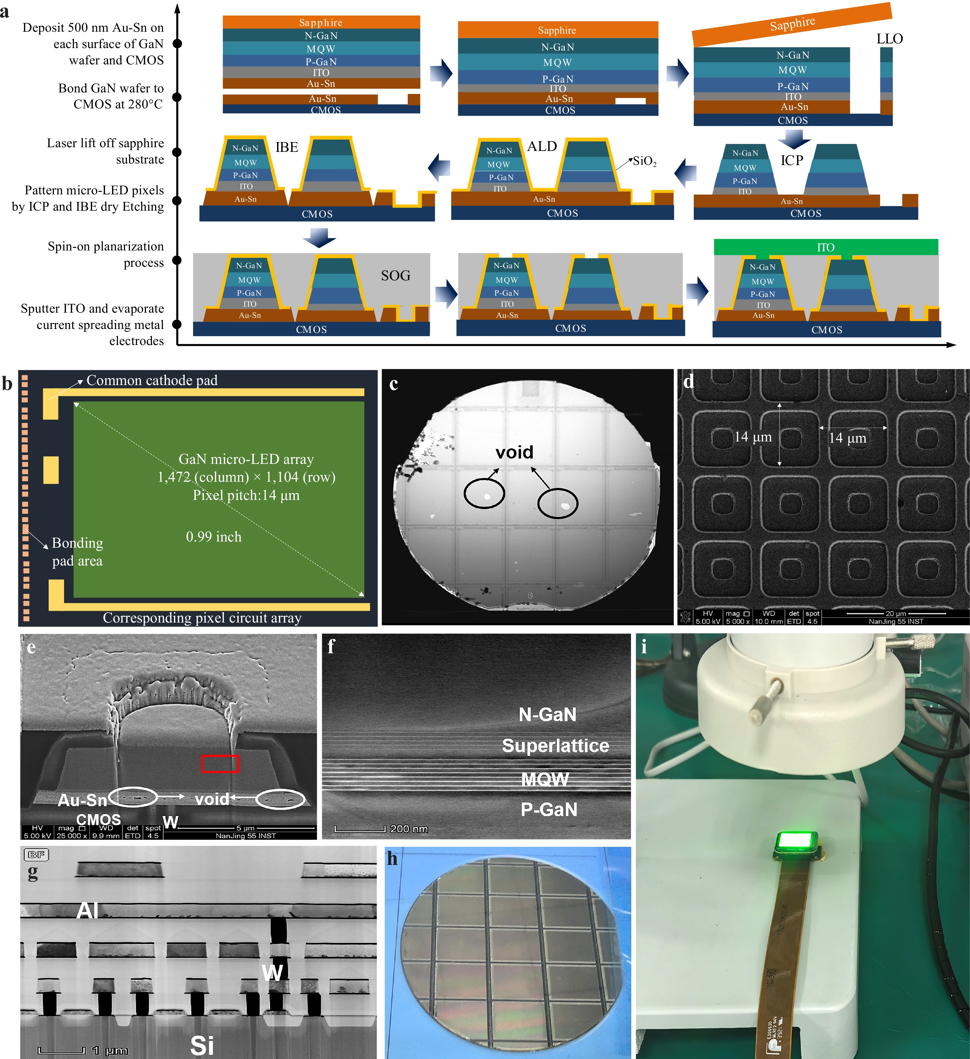
Fig. 2 Fabrication and corresponding process inspections. a Fabrication process of GaN micro-LED heterogeneous integration on Si-based CMOS. b Layout of the micro-LED display. c SAM image of the bonded LED epi-wafer and CMOS wafer. d Top-view SEM image of the micro-LED array. e Cross-section FIB-SEM image of an individual micro-LED. f STEM HAADF cross section image of LED epitaxy and g CMOS. h Photograph of a 4-inch wafer that integrates multiply 0.99-inch green micro-LED displays. i The micro-LED displaying with all pixels on.
Given that the brightness uniformity of a micro-LED display screen is influenced by multiple factors—including the CMOS backplane, compensation algorithms, and process variations—its assessment necessitates a holistic strategy. Consequently, both in-process testing of the optoelectronic properties of the micro-LED and post-manufacturing evaluation of the full display performance must be implemented for a complete analysis. Here we design and fabricate a process monitoring test module bonded on a silicon backplane to evaluate pixel-level leakage currents during micro-LED array integration with the CMOS backplane. Electrical measurements are performed using a probe station after the ICP etching step depicted in Fig. 2a, when the mesa is etched without passivation layer on the micro-LED array. The negative probe is positioned on the mesa top surface, namely n-GaN layer, while the positive probe is placed on the Au bonding layer within the isolation trench.
Fig. 3a shows the I-V characteristics of an individual micro-LED in linear and log scales. The inset plots the reverse saturation current of 50 micro-LEDs at −5 V varies from 0.1 pA to 18.6 pA, indicating a typical low leakage current. Fig. 3b illustrates outstanding electrical uniformity within the micro-LED array, exhibiting a maximum forward current difference of 0.5 μA at 2.6 V and a forward voltage difference of 0.17 V at 1 μA, respectively. This prepared process monitoring test vehicle enables real-time extraction of pixel-level leakage currents during etching step optimization, thereby significantly reducing post-fabrication yield loss of the micro-LED array. In Fig. 3c, the light output power (LOP) shows a linear increase from 0 A to 0.379 A (with a slope of 176.6 mW·A−1), followed by a continued increase at a reduced slope (67.5 mW·A−1) up to 0.625 A, reaching 82.6 mW. The custom-designed CMOS driver can deliver a maximum current of 2 A to the micro-LED display under full-load conditions. Although it enables a theoretically higher LOP, practical factors, such as optimal operating efficiency, thermal management, FPGA control board load capacity, derating strategies, etc., must be considered. Therefore, we limit the total current of the micro-LED display screen to a maximum of 1 A by the driver algorithm code, equivalent to a current density of about 1.25 A·cm−2, to meet the demand of 100-step brightness calibration. The external quantum efficiency (EQE) of the entire micro-LED display screen is calculated from the LOP and plotted in Fig. 3c. The maximum EQE of the whole screen reaches 7.68% at 0.389 A·cm−2 with all pixels on, exceeding the reported 4% at 1.35 A·cm−2 in prior work25. An efficiency droop is observed to reach 6.04% at 0.728 A·cm−2 with the continuously increasing current. This low peak current density indicates that Shockley-Read-Hall (SRH) recombination37–39, dominant under low current densities conditions, is successfully suppressed in our micro-LED array on CMOS, comparable to the previously reported results24. Fig. 3d records the electroluminescence (EL) spectra of the micro-LED display screen with injection currents, showing a full width at half maximum (FWHM) ranging from 35.9 nm to 37.8 nm. The peak wavelength and dominant wavelength were extracted and are shown in Fig. 3e, both of which present a red-shift behavior with the increasing current density. Typically, peak wavelength would be expected to exhibit a blue shift at high current densities, as the polarized electric field is screened by injected carriers, suppressing the quantum confined stark effect (QCSE)34,40,41. This opposite red-shift behavior is attributed to self-heating within the CMOS backplane and micro-LED stack, a phenomenon previously reported in integrated micro-LED displays. Importantly, the broader FWHM under high current densities further confirms the presence of the thermal heating effect in our micro-LED display34,42,43 after taking the causes of current crowding effect, QCSE, nonradiative recombination into consideration4,37. Additionally, thermal heating contributes to the non-linear LOP increase, directly leading to the EQE droop observed in Fig. 3c. Therefore, these findings highlight thermal management as a critical challenge for the integrated micro-LED display screen. Fig. 3f shows the CIE 1931 coordinates (x, y) of the micro-LED display screen at various current densities. The coordinates (x, y) move from (0.2282, 0.7033) to (0.2621, 0.6921) as the current density rises from 0.006 A·cm−2 to 0.703 A·cm−2, with x-coordinate increasing by 0.0339 and y-coordinate decreasing by 0.0112. Notably, this detectable chromaticity shift is quite small, which is below the threshold of visual perceptibility.
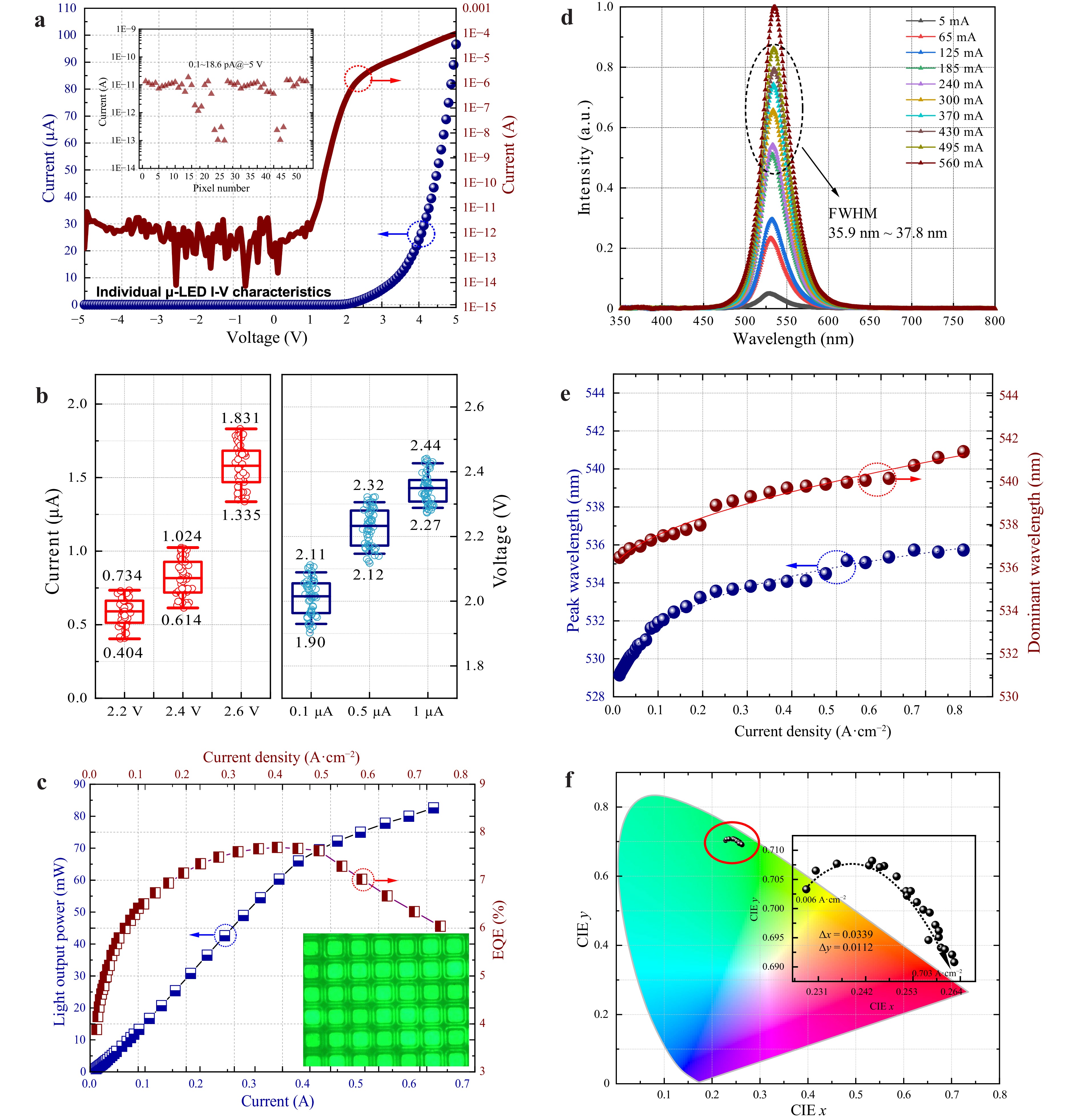
Fig. 3 Optoelectronic performance of micro-LED. a The I-V characteristics of an individual micro-LED pixel in linear scale and log scales. Inset is the leakage currents at −5 V of 50 individual micro-LEDs, varying from 0.1 to 18.6 pA. b Boxplots of injection current and operation voltage of 50 individual micro-LEDs, highlighting excellent electrical uniformity across the micro-LED array. c LOP and EQE of the entire micro-LED display screen versus total injection current and current density respectively. Inset is the emission uniformity image with all pixels on. d The EL spectra of the micro-LED display screen with increasing injection currents, showing a FWHM ranging from 35.9 nm to 37.8 nm. e Peak wavelength and dominant wavelength extracted from the EL spectra, demonstrating the red-shift behavior with the increasing current density. f CIE 1931 coordinates (x, y) of the micro-LED display screen at various current densities.
-
A micro-display with high display uniformity is fabricated via a CMOS driving backplane featuring high current uniformity and a high-efficiency micro-LED process. To characterize the display performance of the CMOS-driven micro-LED display, we use a portable photoelectric measurement system (POMS) to evaluate the average areal brightness (Lave), the in-plane brightness uniformity (Uin-plane) and viewing-angle-dependent brightness characteristics of the micro-LED display (inset of Fig. 4a). We observe an increasing Lave with rising current density, reaching a peak brightness of 20,282 cd·m−2 at 0.5 A·cm−2 (Fig. 4a), which closely mirrors the trend of EQE behavior in Fig. 3c. We attributed the Lave drop to self-heating within the CMOS backplane and micro-LED stack as discussed above. The Uin-plane, calculated as Lmin/Lmax, remains nearly stable at about 90% within the current density range from 0.25 A·cm−2 to 0.5 A·cm−2, which agrees well with the previous CMOS simulation results. The brightness mapping across the whole micro-LED display screen in Fig. 4b exhibits an excellent Uin-plane of 90.12% at 0.5 A full-screen current. Under low-current conditions, stochastic voltage fluctuations across pixels (Fig. 3b) cause some pixels to remain off or exhibit suboptimal luminance, leading to larger brightness difference and low Uin-plane in Fig. 4a at low current densities. This low uniformity is mitigated as current density increases, a phenomenon driven by two factors: first, pixel EQE improves with higher current, as shown in Fig. 3c; second, bright pixels partially compensate for dimmer ones via optical crosstalk. However, with the continuous current increase, thermal effects impede further enhancement of brightness, leading to a certain degree of degradation in the brightness efficiency and uniformity of the display.
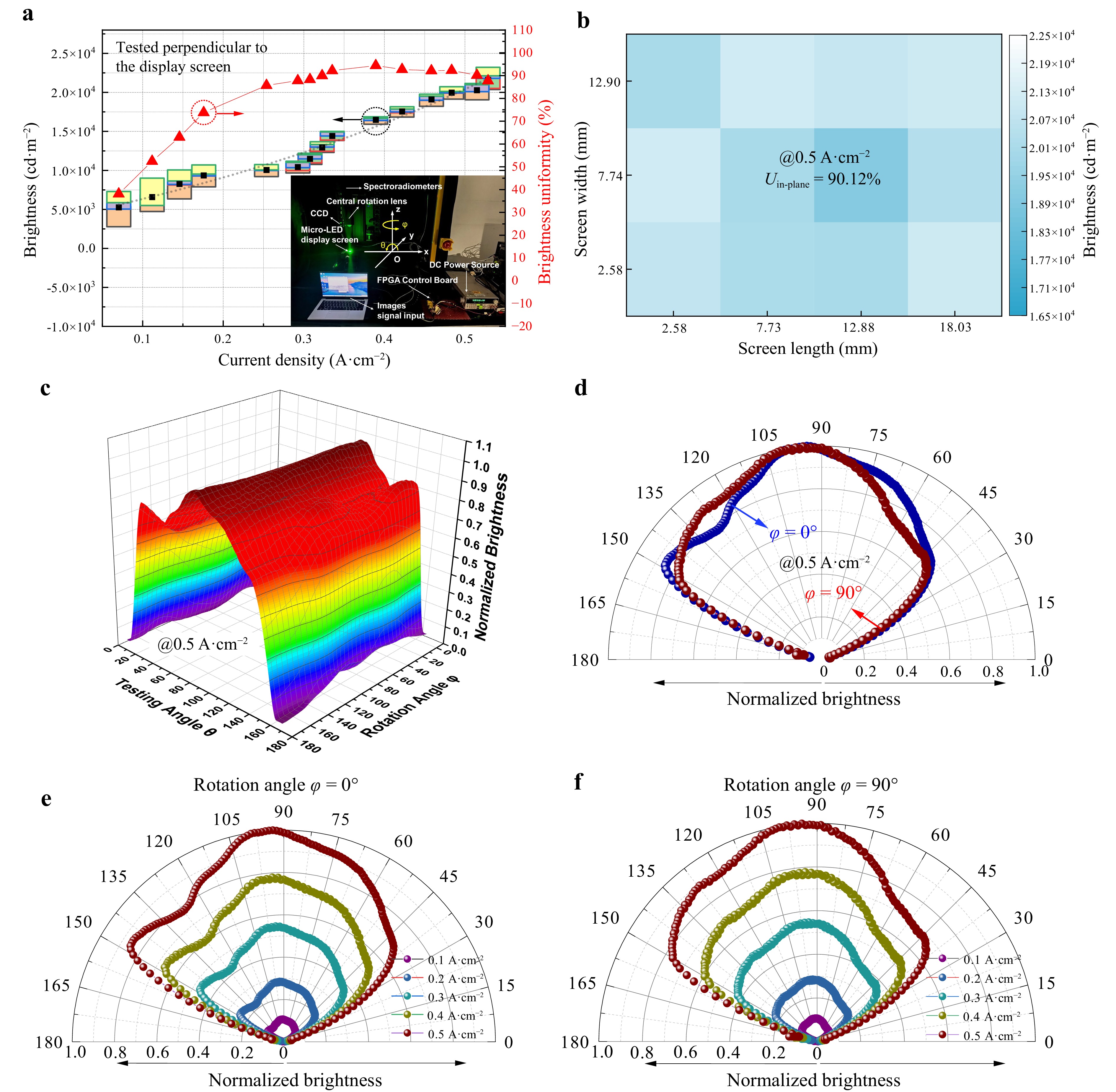
Fig. 4 Display performances of the micro-display screen. a Lave with its corresponding fitting curve and Uin-plane for the entire micro-LED display screen as a function of current density. Inset is the measurement setup to evaluate Lave, Uin-plane, and the viewing-angle-dependent brightness characteristics. b The brightness mapping across the whole micro-LED display screen, exhibiting an excellent Uin-plane of 90.12% at 0.5 A·cm−2. c 3D plot of brightness angular spatial distribution under the current density of 0.5 A·cm−2. d The far-field brightness distribution of the micro-LED display versus horizontal and vertical viewing angles at 0.5 A·cm−2. e The angular dependence of brightness as a function of current density in horizontal direction, measured in a with the rotation angle φ = 0°. f The angular dependence of brightness as a function of current density in vertical direction, measured in a with the rotation angle φ = 90°.
The angular dependence of brightness is a key performance metric for near-eye display applications. Fig. 4c presents 3D plot of brightness angular spatial distribution, measured by POMS using a central rotation lens that incrementally rotated around rotation angle φ and varied testing angle θ at 1° angular resolution (0°−180° for φ, 10°−170° for θ). The far-field brightness distribution of the micro-LED display versus horizontal and vertical viewing angles at 0.5 A·cm−2 in Fig. 4d exhibits nearly identical brightness angular distribution and luminous intensity in both directions. Fig. 4e, f show the angular dependence of brightness as a function of current density in horizontal direction (φ = 0°) and vertical direction (φ = 90°) respectively, indicating high brightness uniformity across 120° viewing angle. Notably, in this work, we do not introduce micro-lens or meta-surface structures44–46 to control the viewing angle and angular brightness distribution, which may be utilized for further optimization.
Fig. 5a displays images of "Nanjing University (NJU) emblem", the scene and diverse grayscale levels, demonstrating high pixel yield and precise grayscale control. The fabricated micro-LED display achieves 8-bit grayscale via the designed CMOS driver, enabling 256 grayscale levels for image rendering. Additionally, we demonstrate a supplementary video at 60 frames per second (fps) for our micro-LED display, showcasing its 60 Hz refresh rate capability. Remarkably, the hardware is capable of supporting higher refresh rates, such as 90 Hz and 120 Hz. Fig. 5b benchmarks the micro-LED displays versus both pixels per inch and size in inches, revealing the capability of our fabricated micro-LED display with remarkable pixel quantity to provide more information with higher resolution.
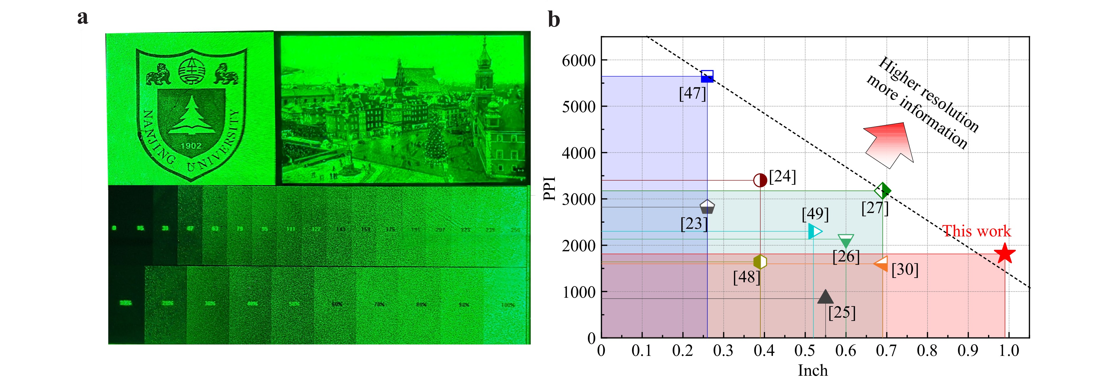
Fig. 5 Demonstration and comparison of the micro-display screen. a Images including "Nanjing University (NJU) emblem", the scene, and the details on grayscale levels displayed on the CMOS-driven micro-LED display screen. b Benchmarks of the CMOS-driven micro-LED displays: PPI vs size (in inches) plots. Our fabricated micro-LED display shows remarkable pixel quantity. The upper right corners refer to the micro-displays of higher resolution with more information.
Here, the ultra-high brightness reported in Ref. 24,27,30 originates from the individual-pixel measurements, which is overestimated compared to the whole display screen measurements. For an individual pixel, the active emission area is defined as the pixel itself, whereas for a display screen, the active emission area includes both emissive pixels and non-emissive gap area. This leads to a lower areal brightness value in calculations for display panels. Here, we emphasize areal brightness (i.e., brightness per unit panel area), which is a critical metric for practical micro-display applications.
As shown in Table 1, references report brightness data at a given current density. Assuming an approximately linear correlation between brightness and current density, we normalize the current density to 1 A·cm−2 for fair comparison. Quantitative analysis indicates that the 0.99-inch micro-LED in this work achieves the highest areal brightness. Accordingly, upon comprehensive comparison with the reported works, our 0.99-inch micro-LED display exhibits the largest active display area, together with the highest areal brightness and best brightness uniformity. Notably, achieving high pixel yield and good brightness uniformity becomes increasingly challenging with increasing pixel count and display size. This excellent display performance further verifies the effectiveness of our strategy in controlling pixel yield and suppressing the IR drop during device operation.
Reference Size (inch) Resolution Active area (mm2) Brightness (cd·m−2) Brightness uniformity This work 0.99 1,472 × 1,104 318.5 a 20,282 @0.5 A·cm−2 90.12%@0.5 A·cm−2 23 0.26 640 × 360 18.7 N/A N/A 24 0.39 1,024 × 768 44 b 1.7 × 10⁶ @4,211 A·cm−2 N/A 25 0.55 400 × 240 86.4 c 8,300 @0.61 A·cm−2 N/A 26 0.6 1,024 × 768 113.2 d 9.85 @2.46 A·cm−2 N/A 27 0.7 1,920 × 1,080 132.7 e 3.07 × 10⁴ @277.8 A·cm−2 N/A 30 0.69 960 × 540 132.7 f 6.5 × 10⁵ @1,000 A·cm−2 N/A 47 0.26 1,080 × 960 21 g 4 × 10⁵ @100 × 100 pixel N/A 48 0.39 512 × 384 44.2 c 10,591.8 @2.1 A·cm−2 50.79% @2.1 A·cm−2 49 0.52 1,056 × 586 72.2 c 6.7 × 10⁴ @3.7 A·cm−2 59.3% @3.7 A·cm−2 a Typical value of the whole display screen; b Measured value of an individual green micro-LED; c Maximum value of the whole display screen; d Calculated based on the relevant data presented in Ref. 26; e Measured value of an individual blue micro-LED; f Measured value of an individual red micro-LED; g The current corresponding to the brightness of this array is not specified in Ref. 47. Table 1. Display performance comparison of the micro-LED display screen.
-
In summary, we have successfully demonstrated a high-resolution and high-brightness uniformity 0.99-inch micro-LED display with exceeding 1.62 million pixels by the heterogeneous integration of green GaN-based micro-LEDs on custom Si CMOS platform. The superior performance of this device is attributed to the synergistic optimization of circuit architecture and fabrication process. Specifically, the driving circuitry achieves state-of-the-art linearity with DNL and INL below 0.004 LSB, ensuring precise current regulation across the entire array. Furthermore, by systematically mitigating interfacial stress and thermal mismatch, we effectively suppressed bonding void formation, wafer bowing. As a result, the display delivers a peak brightness exceeding 20,000 cd·m−2 and a high brightness uniformity of 90.12%. The viewing angles are as wide as 120° in both horizontal and vertical directions. This display prototype demonstrates full compliance with key target specifications for engineering applications, thereby paving the way for the future development of micro-LED technology in near-eye display.
-
We performed circuit simulations using Cadence. Firstly, for the pixel circuit simulation, we fitted the I-V characteristics of the LED and constructed a model file based on a piecewise high-order function, which was incorporated into the pixel circuit for simulation. A frame period was set to 60 Hz (16.6 ms), and each frame was divided into 8 subframes by weight corresponding to the input 8-bit data. A data bit with the corresponding weight of 1 indicates that the pixel circuit is turned on during that subframe, and vice versa. Data ranging from 00 to FF was applied at the input for simulation, and the average current flowing through the LED within one frame was statistically analysed, yielding the simulation results shown in Fig. 1a. The current values through the LED were sampled and calculated using the DNL and INL functions in Cadence Calculator, resulting in the results presented in Fig. 1b. Secondly, for the uniformity simulation, the Monte Carlo simulation tool in Cadence was utilized to simulate the current through the LED, with a sample size of 200 and static parameter mismatch selected. The simulation yielded the results in Fig. 1c. A complete row-column circuit was constructed, and distributed parasitic resistances were added to the power supply and common cathode power supply of the pixel array. A total of 256 points were uniformly selected across the entire pixel array, and the current of these 256 pixels was simulated and statistically analysed, resulting in the results shown in Fig. 1d.
-
After epitaxial growth, the wafer is coated with ITO (100 nm) onto p-GaN by EBE and annealed in N2 ambience at 550℃ for 480 seconds by rapid thermal annealer (RTA), and then a 500 nm thick Au/Sn metal stack layer is deposited by EBE on the surface of the p-GaN layer and the interconnect pads of the CMOS panel, respectively, which are well bonded at a temperature of 280 ℃ and a pressure of 78 kN for 1 hour. The epitaxial sapphire substrate is then removed using a laser LLO process using LLO System (model: 10LALL005CB) by Maxwell Technology (Zhuhai) Co., Ltd, which utilized a 266-nm laser with an energy density of 220 mJ·cm−2 and a pulse frequency of 200 kHz. High resistance buffer layer is removed by immersion in a 10% dilute hydrochloric acid solution at 25 °C for 10 min. GaN mesa is achieved through photolithography with a stepper lithography machine (NSR-2205i11, Nikon) and etching processes using BCl3/Cl2 gas with ICP. 200 nm SiO2 was further deposited using ALD (TFS 200, Beneq). The Au-Sn bonding metal is patterned by IBE with the subsequent SOG resist spin-coated on the wafer. After opening the window on the top of mesa, current spreading layer (100 nm ITO) is deposited onto n-GaN layer by sputter without annealing, and then a 1.5-μm thick Ti/Pt/Au/Ti metal stacks layer is deposited as common cathode electrode by EBE. Finally, the display screen was wire-bonded onto a PCB by wire bonder (BJ855, HESSE).
-
The optical images of the micro-LED were characterized through a microscope (Zeiss Axio Scope A1) and a camera of pura 70 pro. The SEM images were characterized by the field-emission SEM (Regulus SU8230). The cross-section image was obtained by FIB-SEM (Quanta 3D FEG). The STEM HAADF images were acquired with a transmission electron microscope (Talos F200X). The optoelectronic performance characterization was conducted using a self-built probe station (Everbeing) with a Keithley 2636B for current source, and a spectrometer (Ocean Insight QEpro) with a Keithley 2400 for current source. The display performance of the micro-display screen was measured using the POMS system. A central rotation lens equipped with a CCD, aligned with the display surface normal, was incrementally rotated in horizontal (θ//) and vertical (θ⊥) directions at 1° angular resolution. A goniometric imaging colorimeter (Vantage-6100UL) collected emission from the micro-LED display, with data transmitted to a computer for post-processing. In order to more accurately evaluate the perceived brightness values of micro-LED screen, the luminance meter was positioned at a minimum distance of 55 mm from the measured surface, thereby integrating the non-illuminated areas between pixels into the measurement.
-
This work was supported by the National Key Research and Development Program of China (2024YFB3613000), the National Nature Science Foundation of China (62274083, T2221003, 62474087, 624B2064), Natural Science Foundation of Jiangsu Province (BK20232042, BK20232024), China Postdoctoral Science Foundation under Grant (BX20240164), the Fundamental Research Funds for the Central Universities (XJ2024005803), Collaborative Innovation Center of Solid-State Lighting and Energy-Saving Electronics. We also thank Chongqing Konka Optoelectronics Technology Co., Ltd for some manufacturing process support.
Towards high-resolution and high-brightness uniformity near-eye display: heterogeneous integration of GaN-based micro-LED on a custom Si CMOS platform
- Light: Advanced Manufacturing , Article number: 103 (2026)
- Received: 16 December 2025
- Revised: 31 May 2026
- Accepted: 21 June 2026 Published online: 29 June 2026
doi: https://doi.org/10.37188/lam.2026.103
Abstract: Micro-light-emitting diode (micro-LED) displays are prime candidates for near-eye displays, where increasing the panel diagonal at a fixed pixel density is essential to expand the field of view. However, scaling the active area while maintaining luminance homogeneity presents a challenge, primarily due to the pixel-to-pixel current variation in CMOS driven and process-induced non-uniformities in LED arrays. Here we address this trade-off by combining per-pixel current regulation with an optimized fabrication flow in a heterogeneous integration strategy that couples green GaN-based micro-LED with a custom Si CMOS backplane via wafer bonding. The resulting 0.99-inch prototype (1,472 × 1,104 pixels, 14 µm pitch, 1,814 PPI) exhibits >90% brightness uniformity across the active area, peak luminance exceeding 20,000 cd·m−2, a wide viewing angle (>120°), and excellent electrical consistency. These results demonstrate that our heterogeneous integration approach can chart a path toward larger, uniform, and power-efficient micro-displays.
Research Summary
Optoelectronics: Heterogeneous Integration Empowers High-performance micro-displays
Larger and brighter micro-LED screens could help make future augmented-reality glasses feel more immersive, but keeping every tiny pixel equally bright becomes difficult as the display grows. Small differences in the electronic driving circuit and in the LED fabrication process can make some areas appear brighter or dimmer than others. Zhe Zhuang from China’s Nanjing University and colleagues now report combining green GaN micro-LEDs with a custom silicon CMOS backplane through wafer bonding to precisely control the current for every individual pixel. They also improve the manufacturing process to reduce variations across the display. The resulting prototype shows highly uniform brightness across a relatively large active area while maintaining strong light output and a wide viewing angle. This work offers a practical route toward larger, clearer, and more energy-efficient micro-displays for next-generation near-eye devices.
Rights and permissions
Open Access This article is licensed under a Creative Commons Attribution 4.0 International License, which permits use, sharing, adaptation, distribution and reproduction in any medium or format, as long as you give appropriate credit to the original author(s) and the source, provide a link to the Creative Commons license, and indicate if changes were made. The images or other third party material in this article are included in the article′s Creative Commons license, unless indicated otherwise in a credit line to the material. If material is not included in the article′s Creative Commons license and your intended use is not permitted by statutory regulation or exceeds the permitted use, you will need to obtain permission directly from the copyright holder. To view a copy of this license, visit http://creativecommons.org/licenses/by/4.0/.

 DownLoad: