
2023 Vol. 4, No. 4
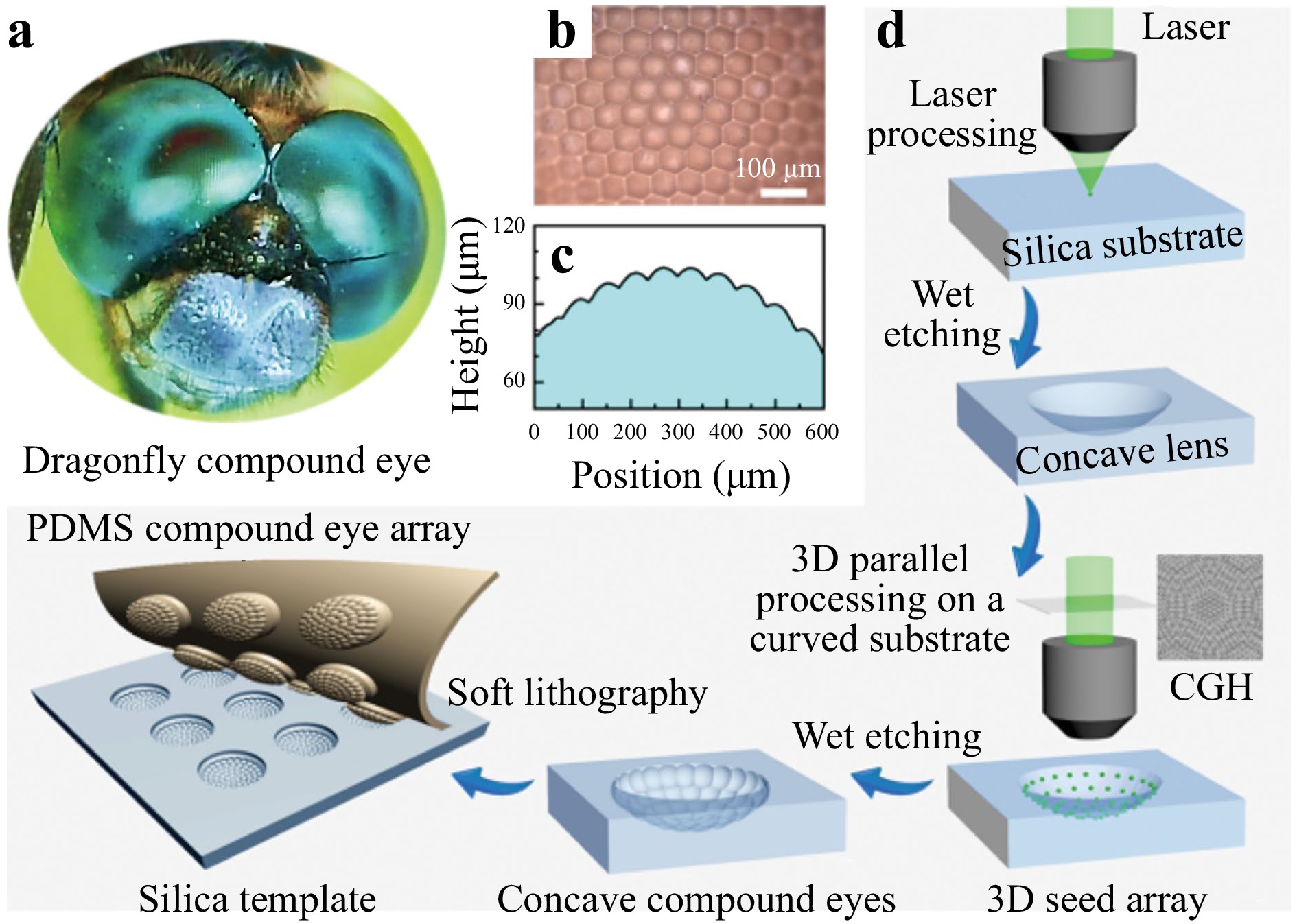
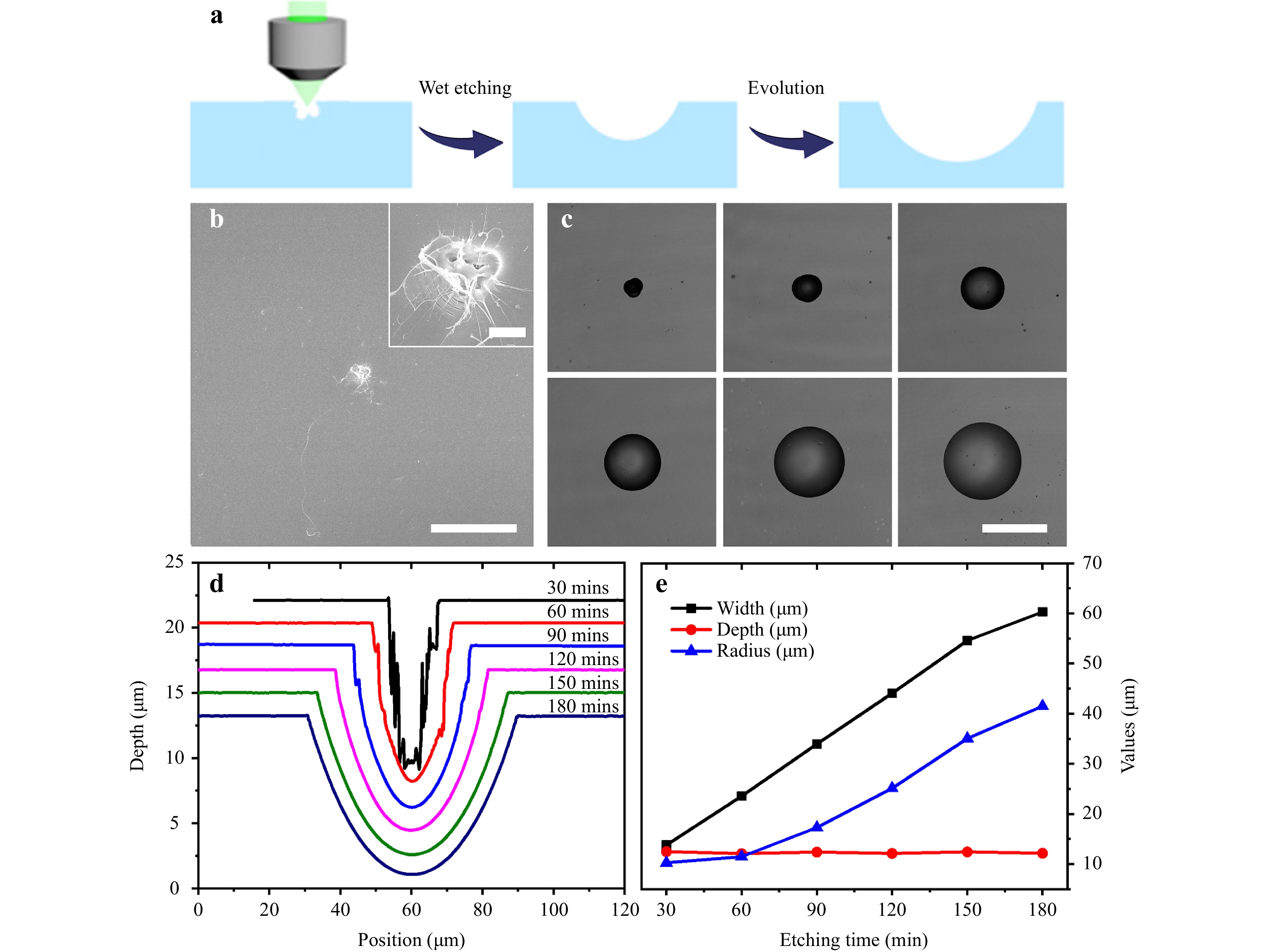
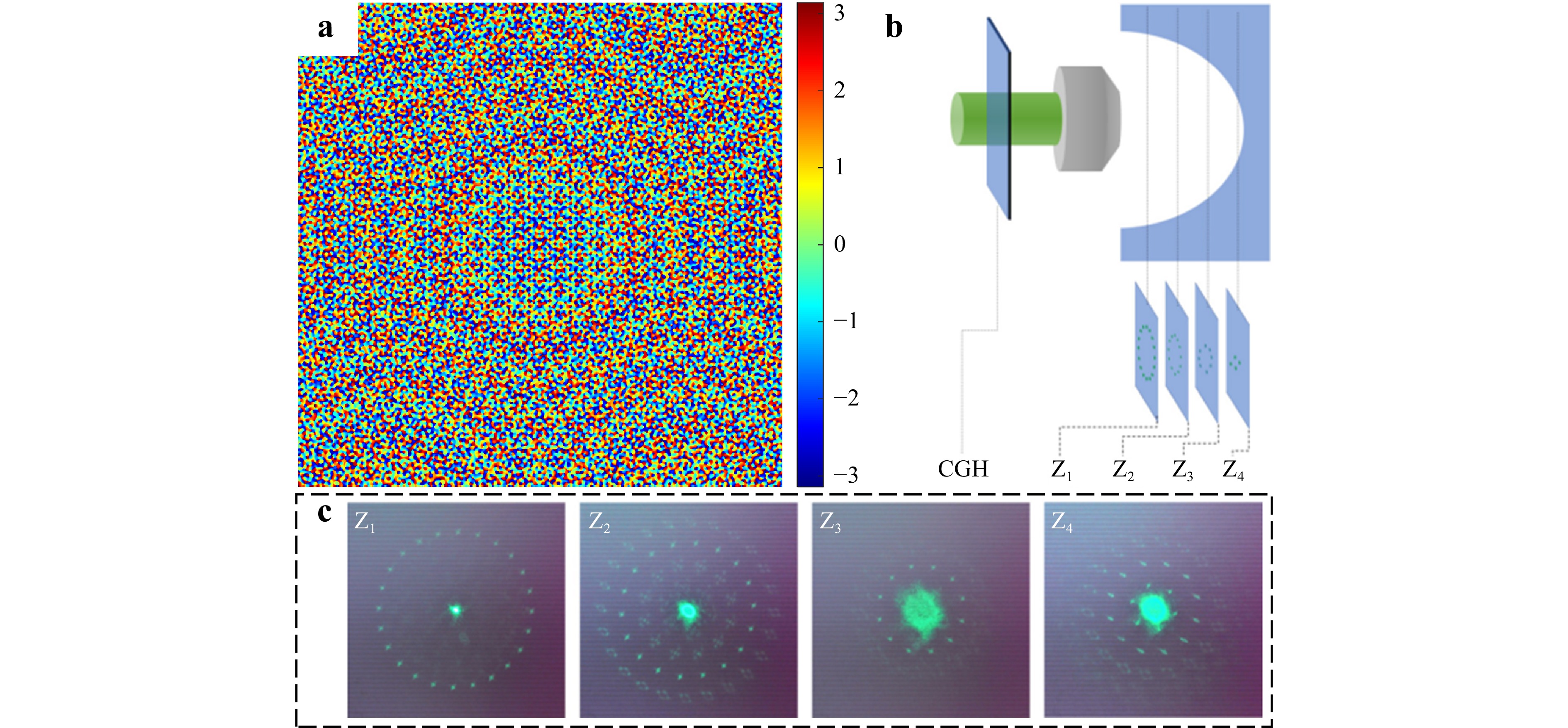
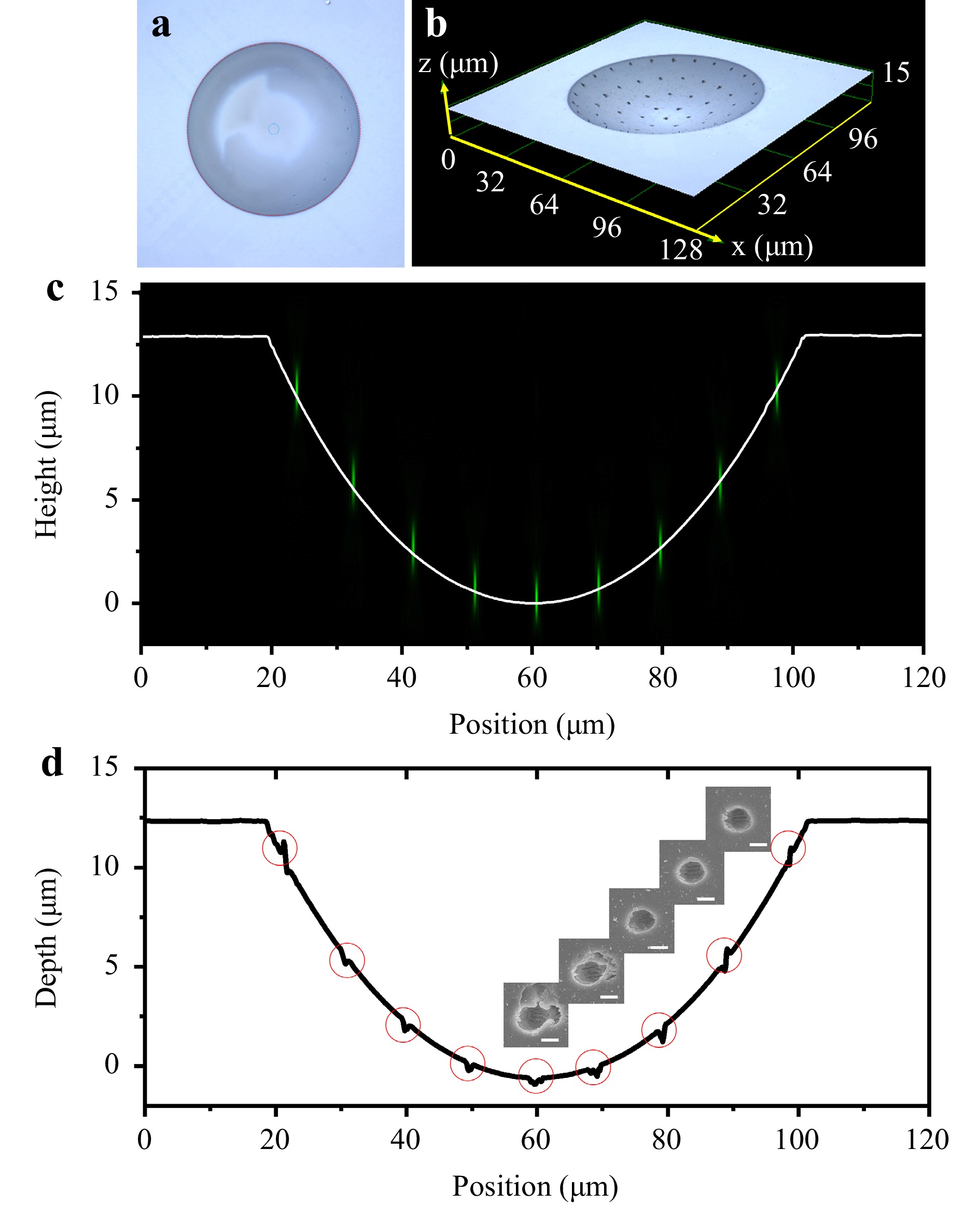
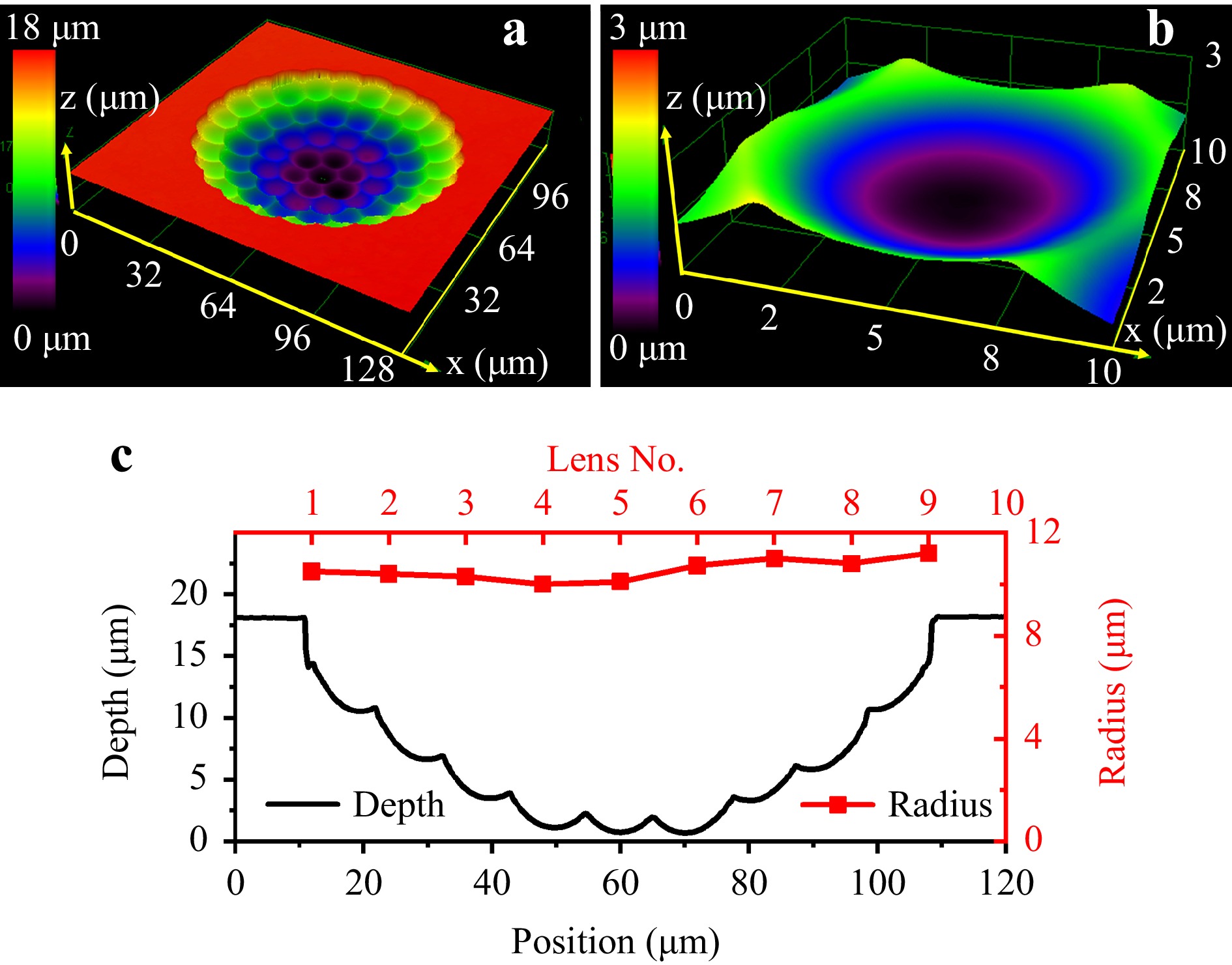
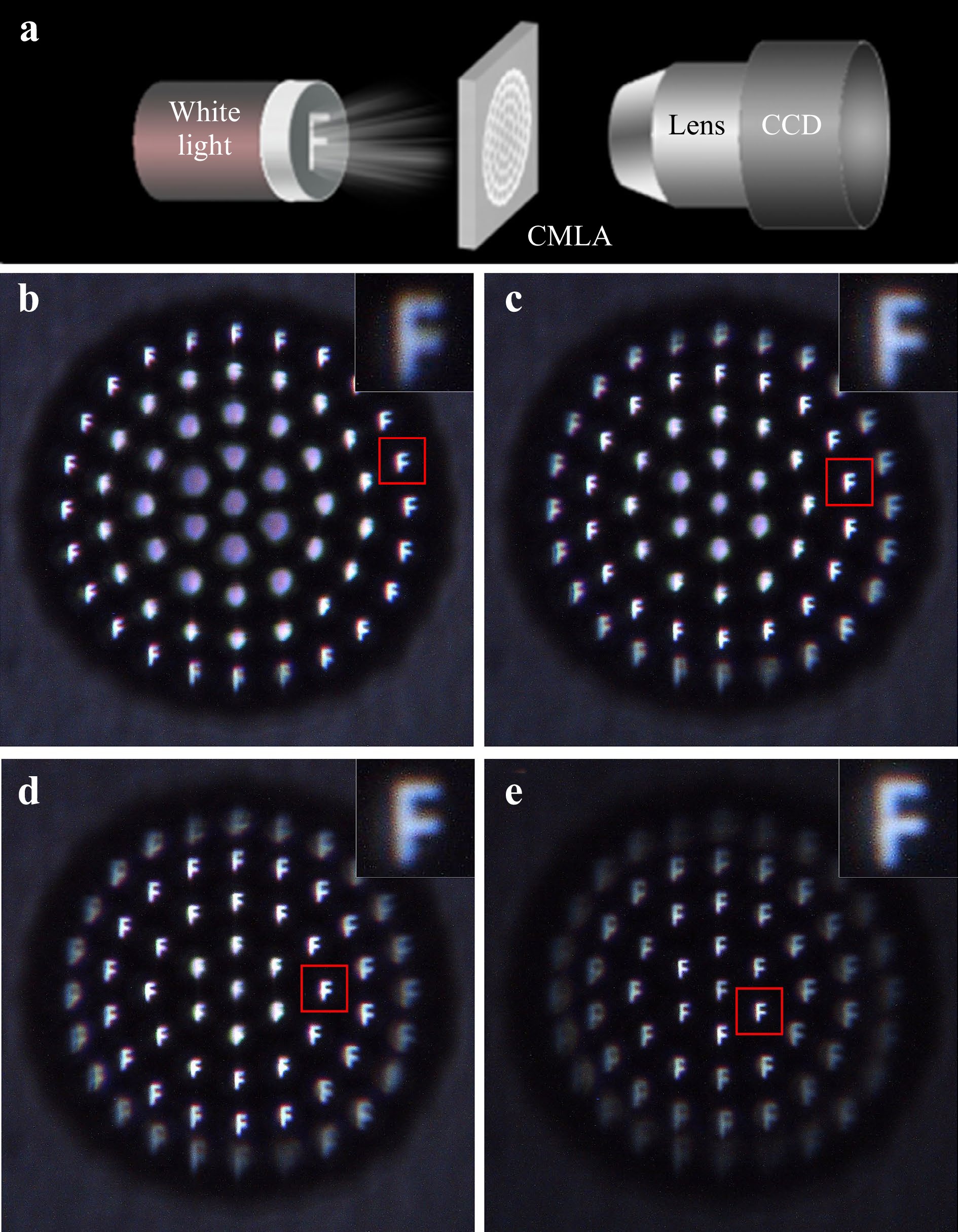
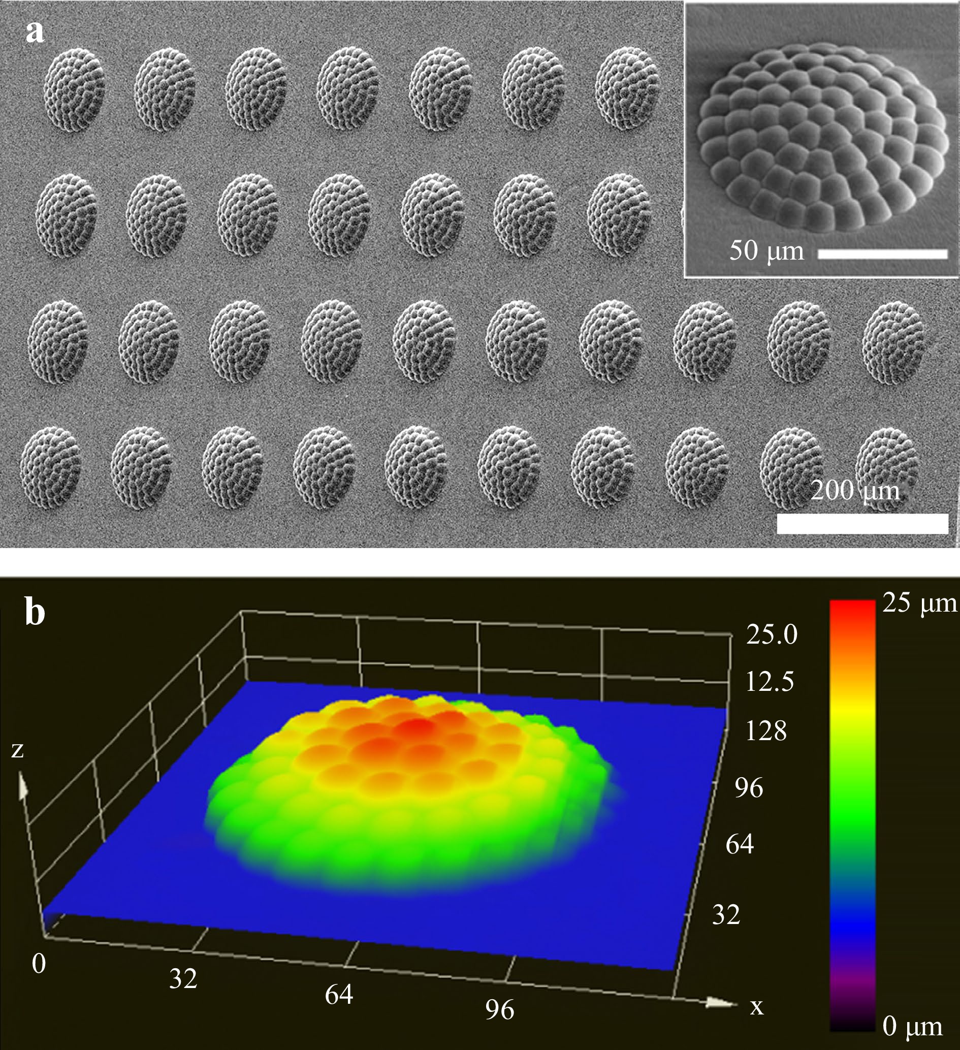
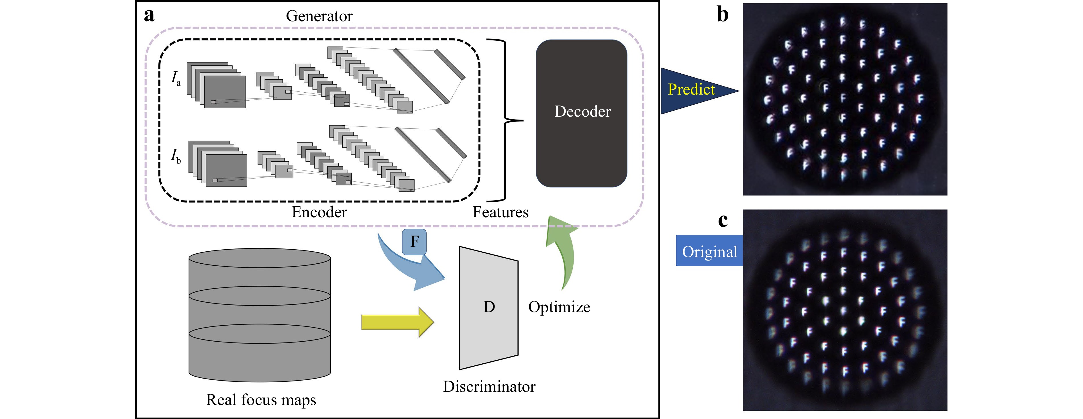
The demand for fast optical image acquisition without movable optical elements (e.g., for self-driving car technology) can be met using bioinspired 3D compound eyes. 3D laser processing strategies enable designable 3D structuring but suffer from low fabrication efficiency, which significantly limits their applications in producing complex 3D optical devices. Herein, we demonstrate a versatile yet simple wet-etching-assisted holographic laser fabrication method for the development of 3D compound eyes. Artificial compound μ-eyes can be readily fabricated by programming a 3D spot array for the parallel ablation of a curved fused silica surface, followed by controllable etching in a hydrofluoric (HF) acid solution. A 3D-concave-lens array made on a curved surface over an area of 100 μm cross-section with each lenslet of 10 μm radius was fabricated with high fidelity and excellent imaging/focusing quality. The resultant 3D-concave-lens can serve as a hard template for the mass production of soft compound eyes through soft lithography. Additionally, using a generative adversarial network (GAN)-based deep learning algorithm, image restoration was conducted for each lenslet, which retained a large field of view and significantly improved image quality. This method provides a simple solution to the requirements of compound μ-eyes required by Industry 4.0.
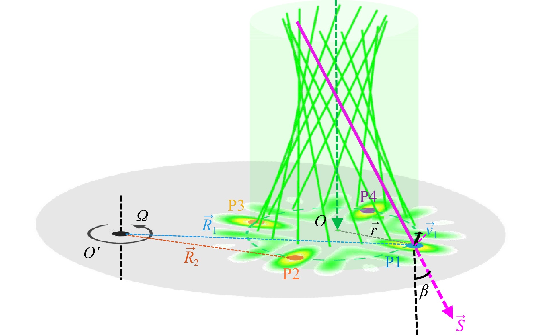
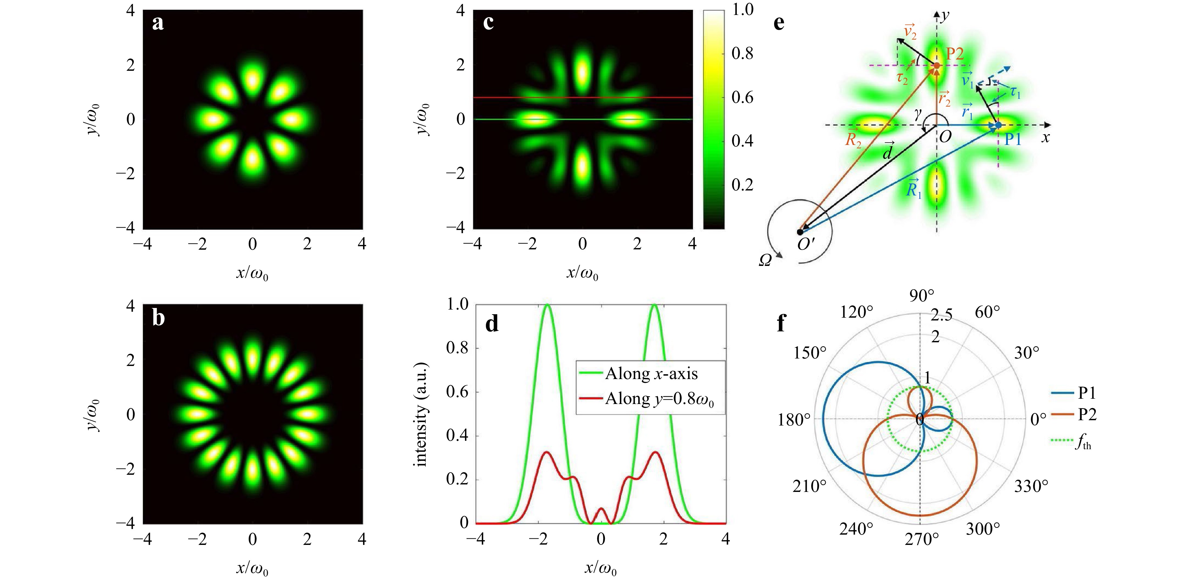
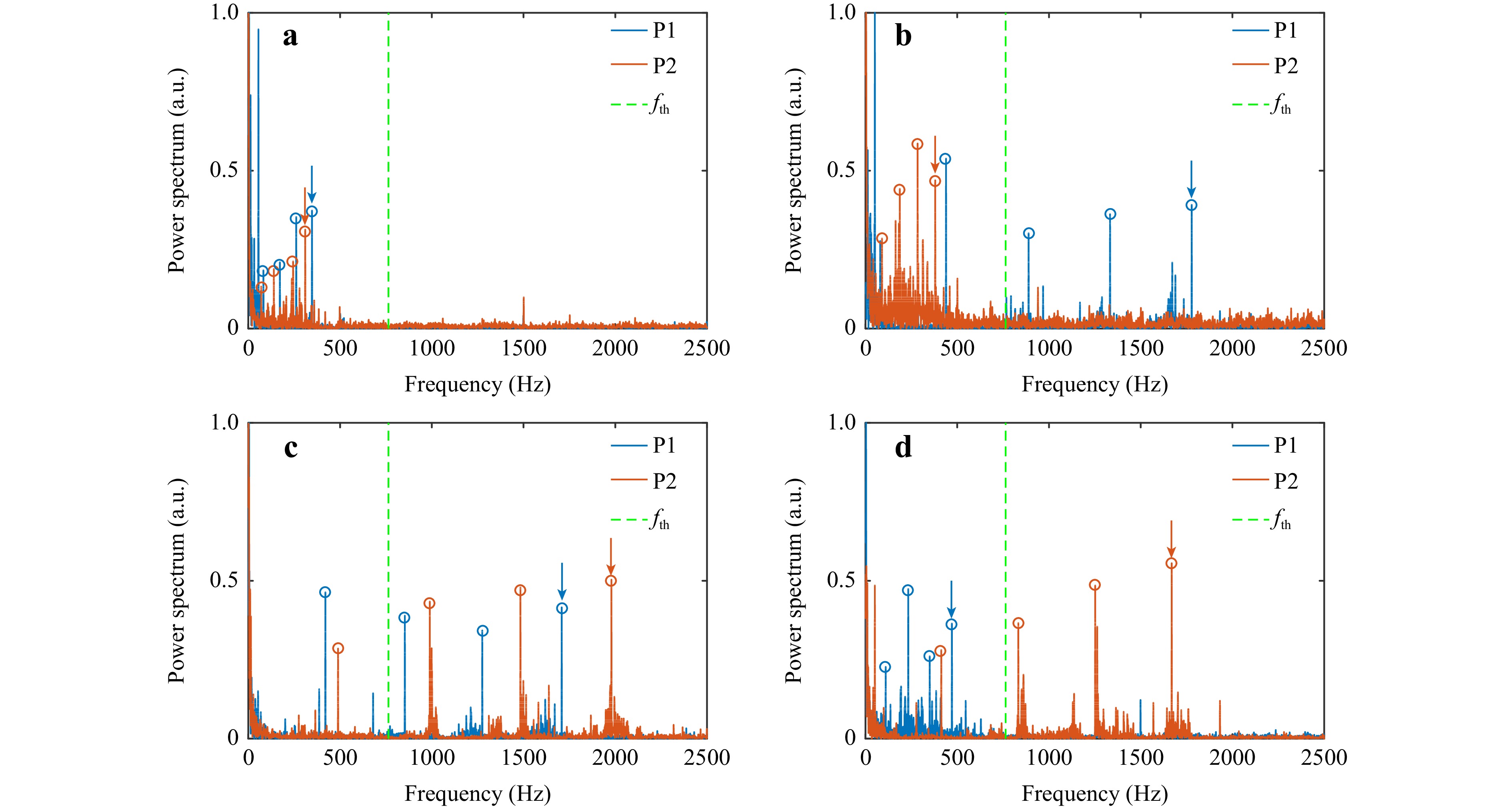
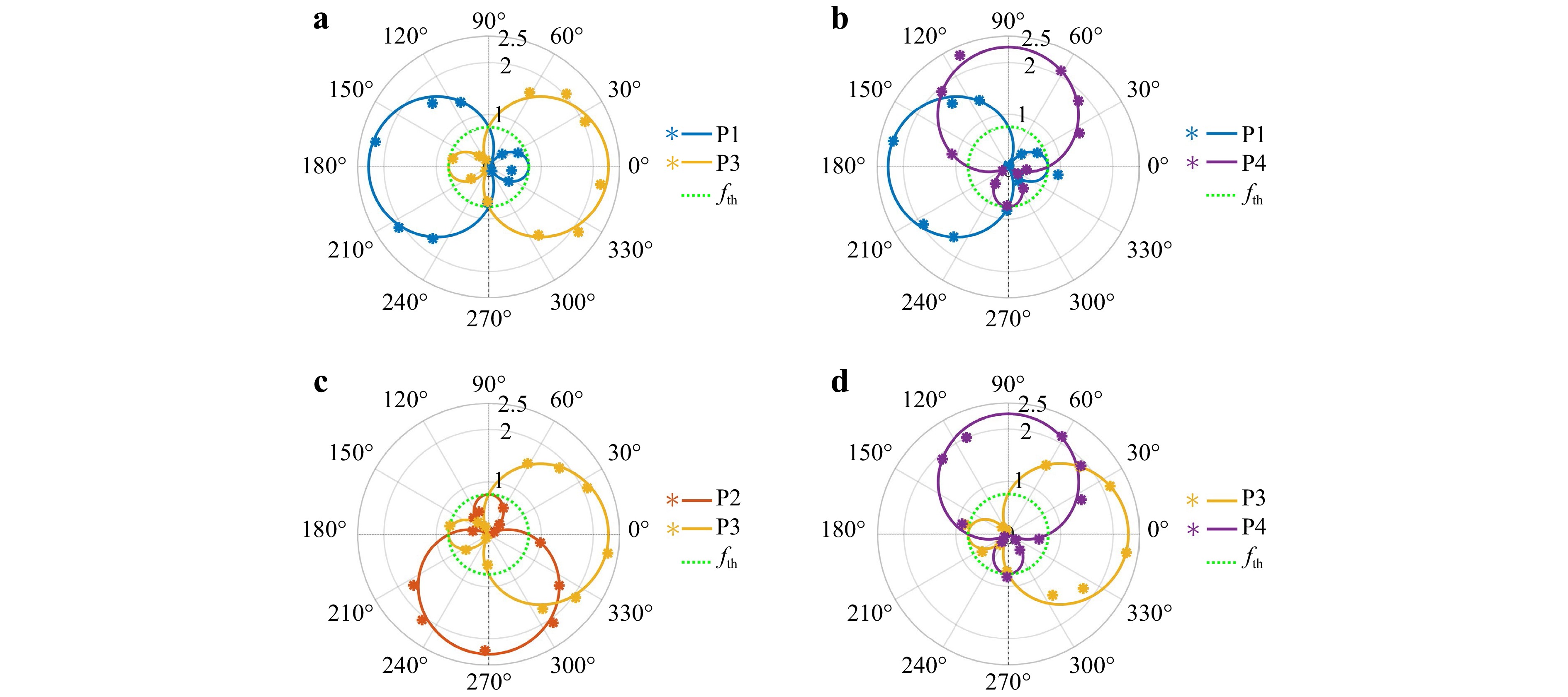
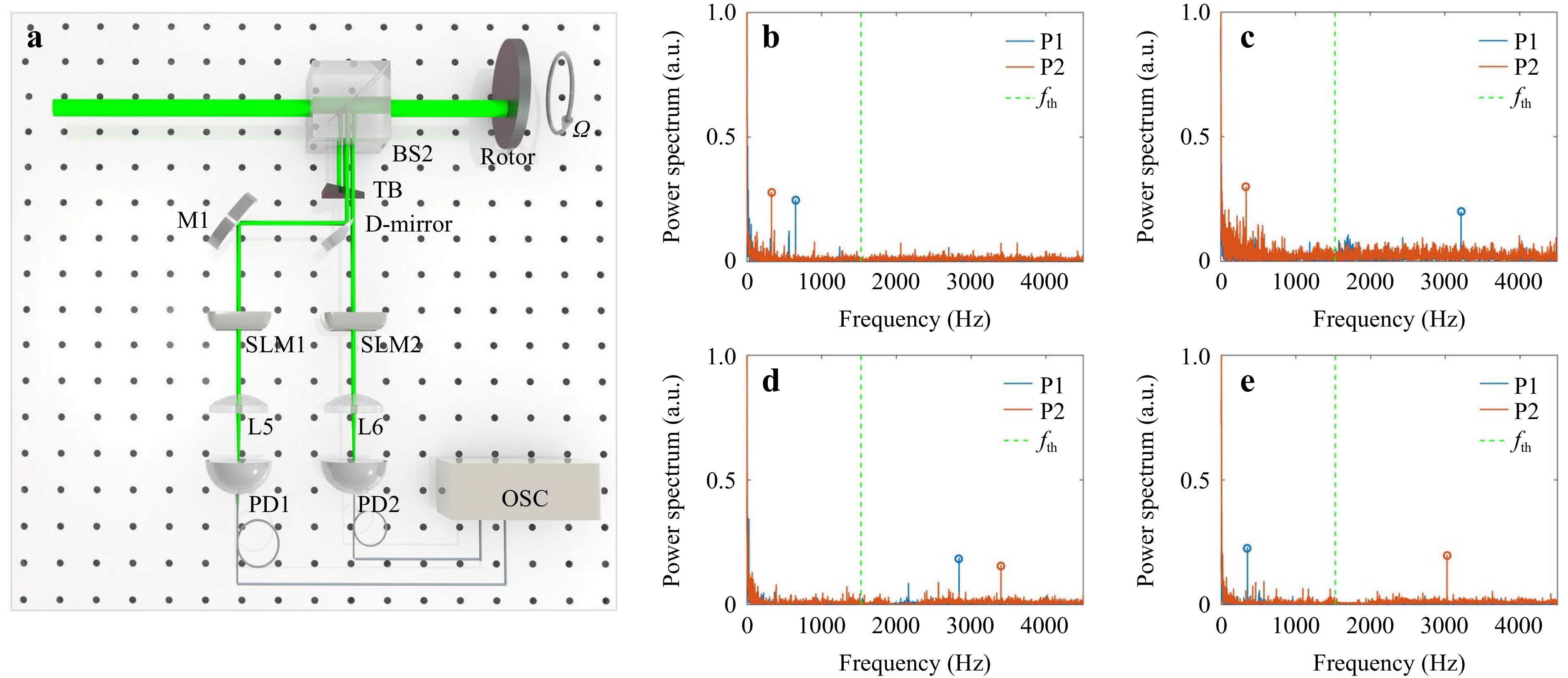
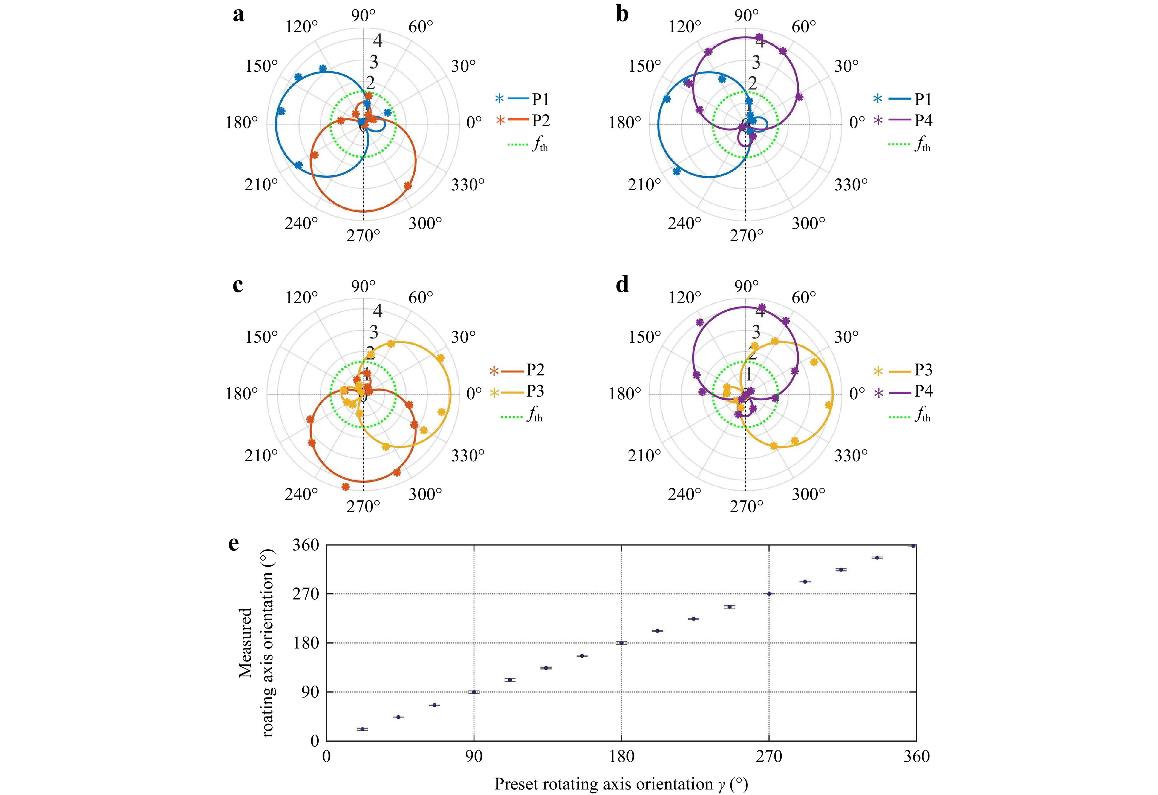
Probing the axis of a rotator is important in astrophysics, aerospace, manufacturing, machinery, automation, and virtual reality, etc. Existing optical solutions commonly require multiple sequential measurements via symmetry-broken light fields, which make them time-consuming, inefficient, and prone to accumulated errors. Herein, we propose the concept of a dual-point noncoaxial rotational Doppler effect (DNRDE) and demonstrate a one-shot detection technique to solve this problem. An on-demand synthetic orbital angular momentum (OAM) light beam impinges on a rotating scatterer surface, supporting dual-point rotational Doppler shifts, in which the information of the rotating axis is acquired by comparing these two frequency shifts with a prescribed threshold. The existence of arbitrary dual-point Doppler shifts enables the one-time direct identification of rotating axis orientations, which is fundamentally inaccessible in single-point detection. This robust detection technique is compatible with generalised synthetic OAM light fields by utilising optical modal filters. Compared with traditional approaches, our DNRDE-driven detection approach exhibits a four-fold enhancement in measurement speed, higher energy efficiency, and superior accuracy with a maximal absolute measurement error of 2.23°. The proposed dual-point detection method holds great promise for detecting rotating bodies in various applications, such as astronomical surveys and industrial manufacturing.
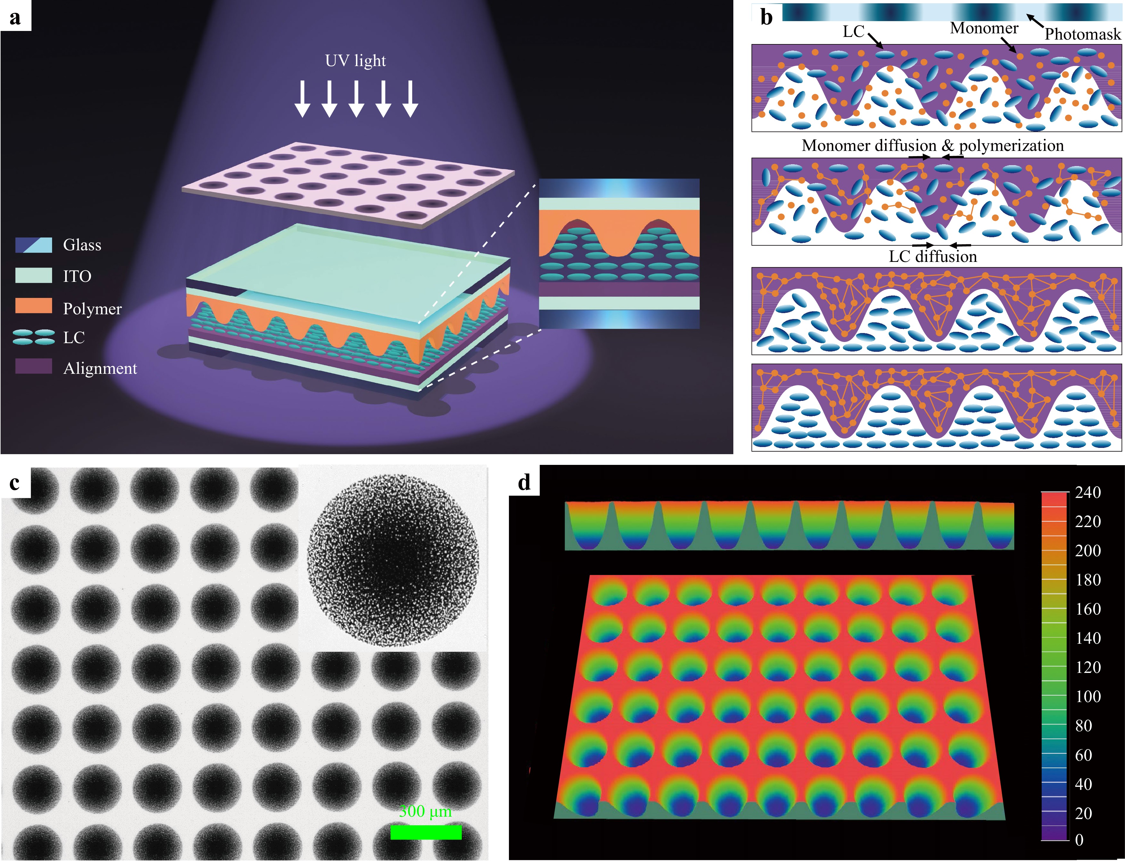
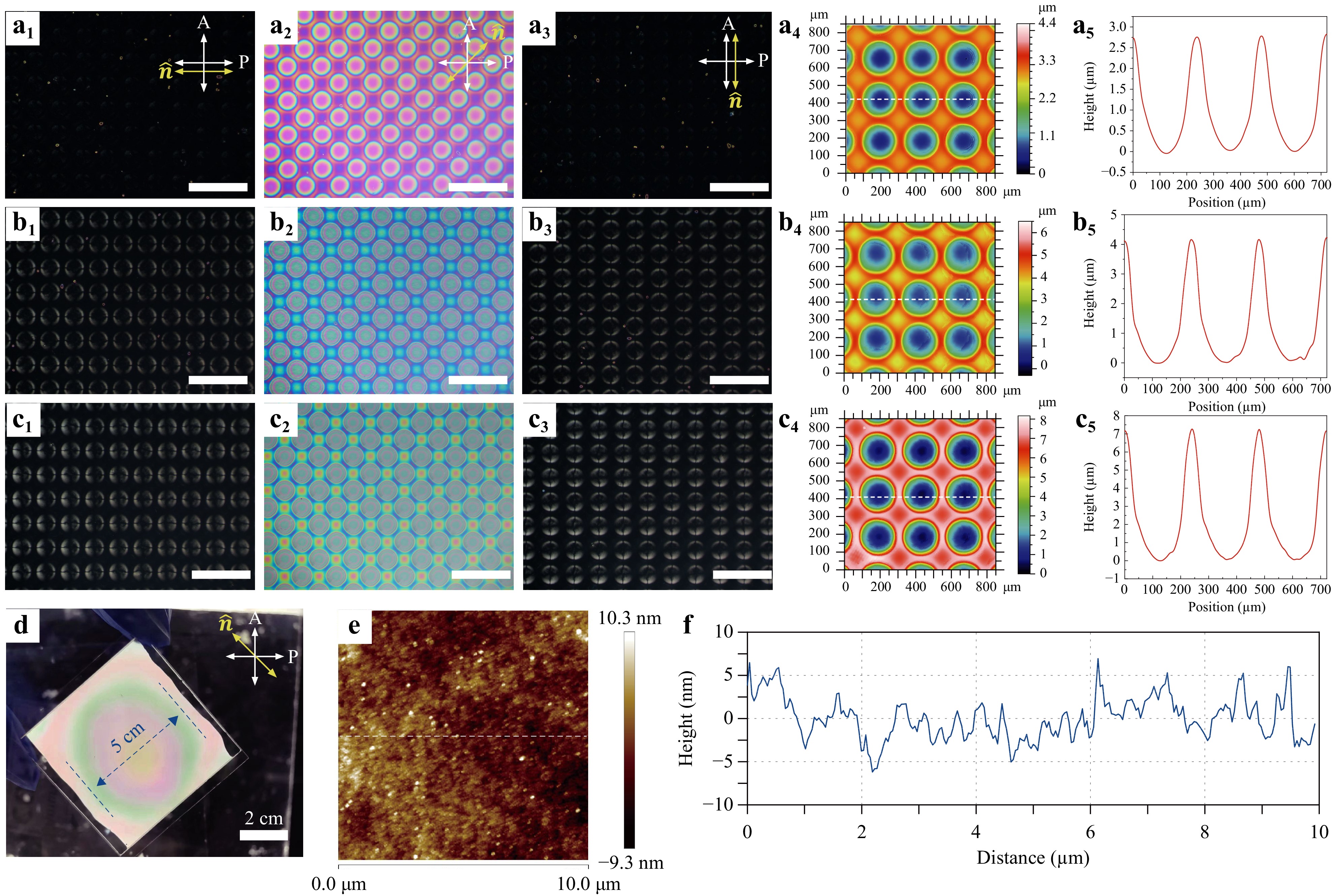
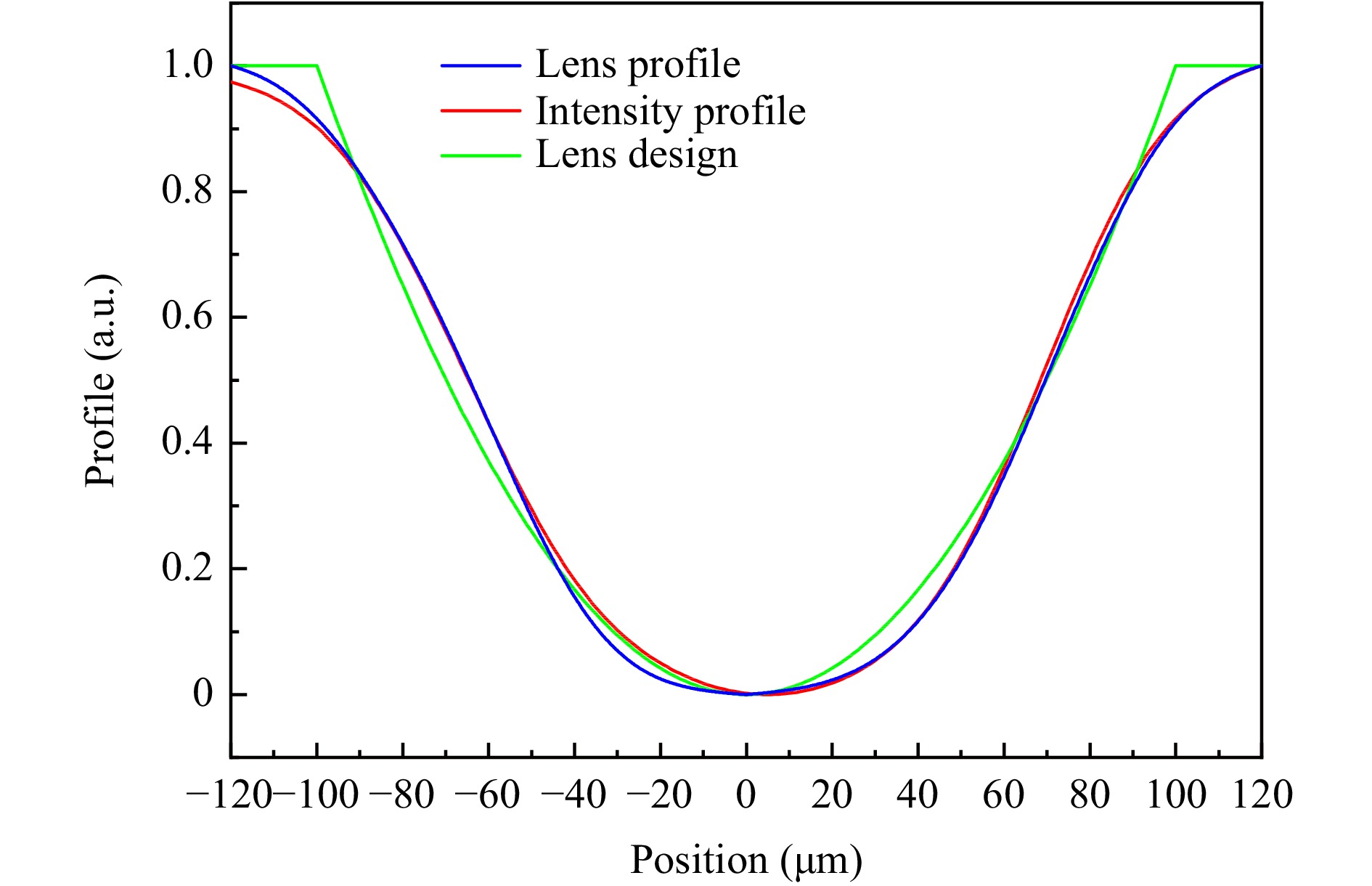
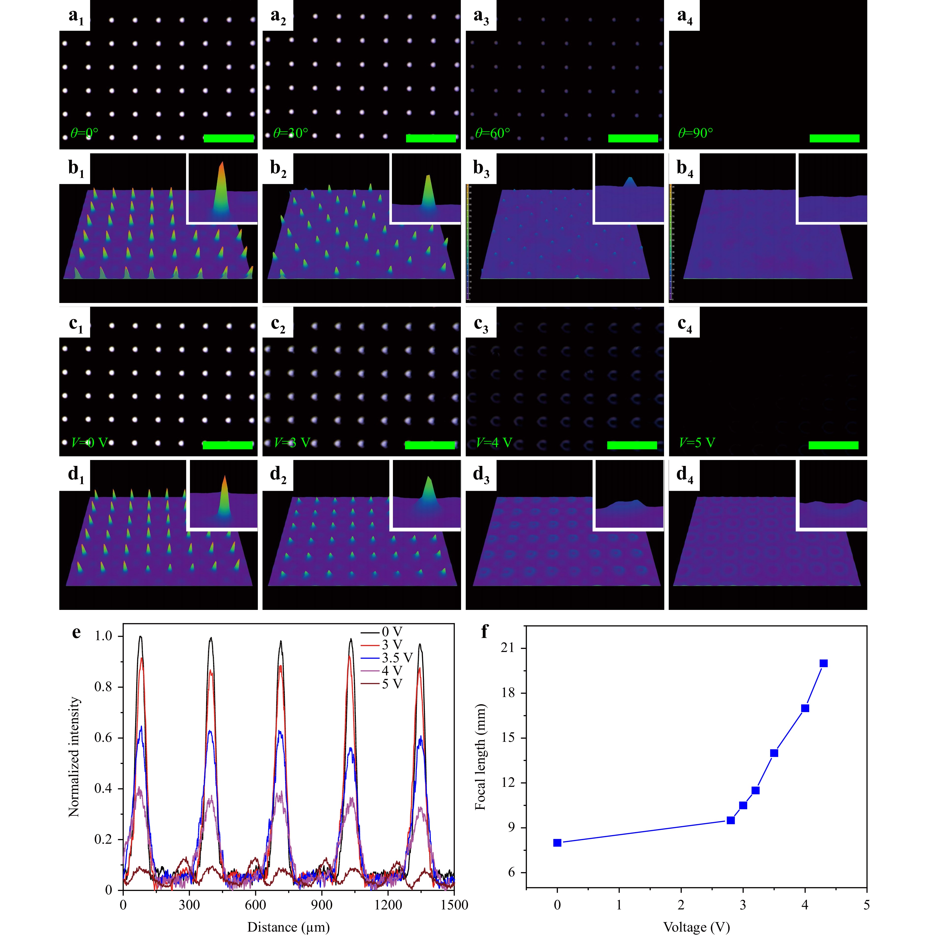
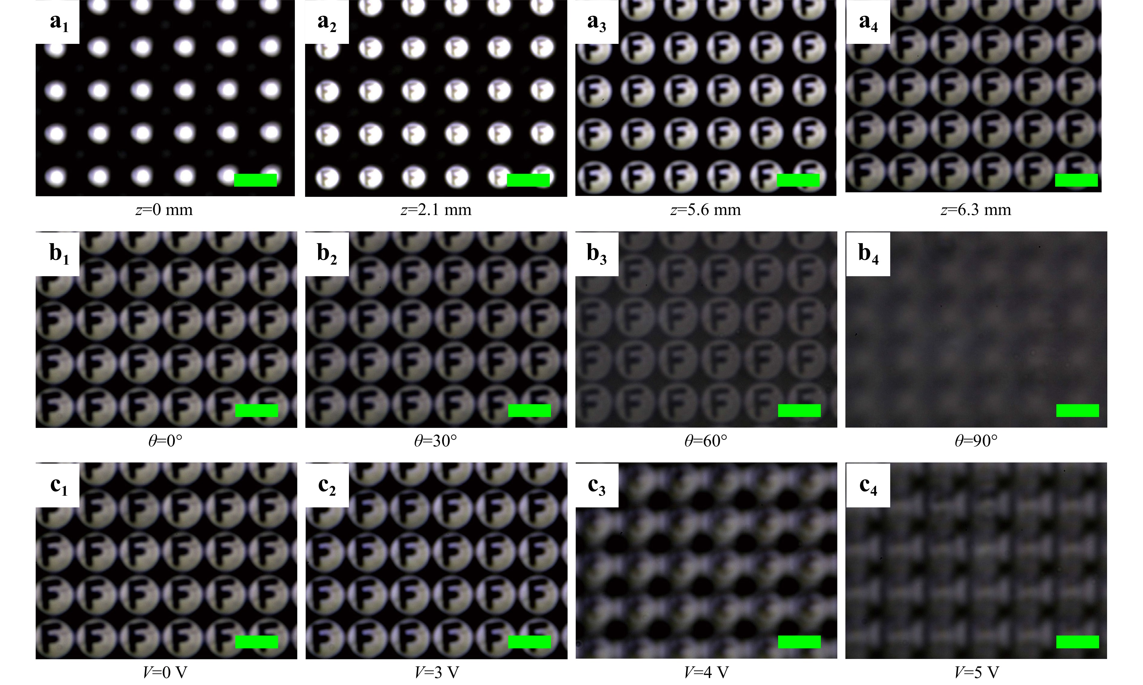
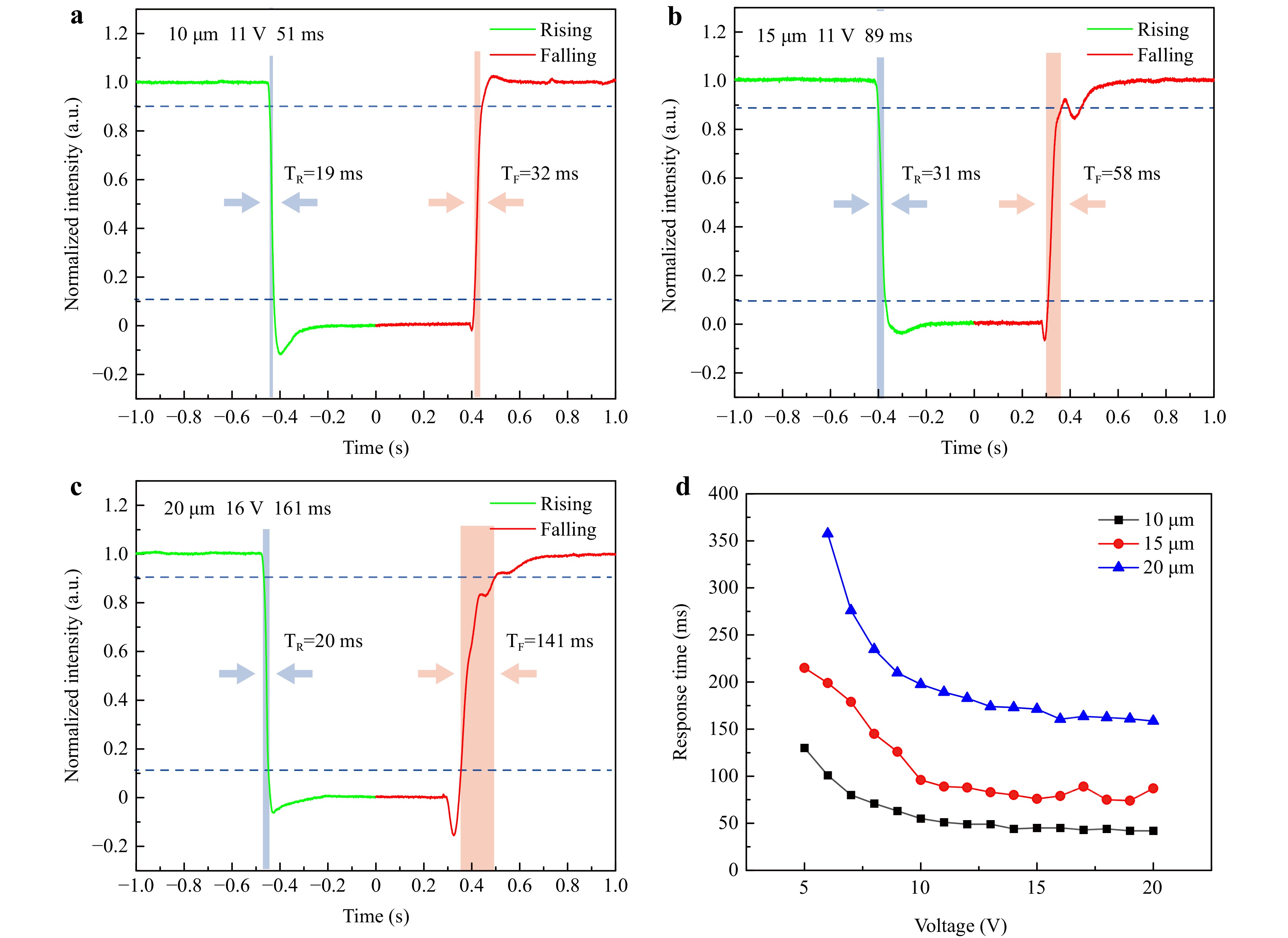
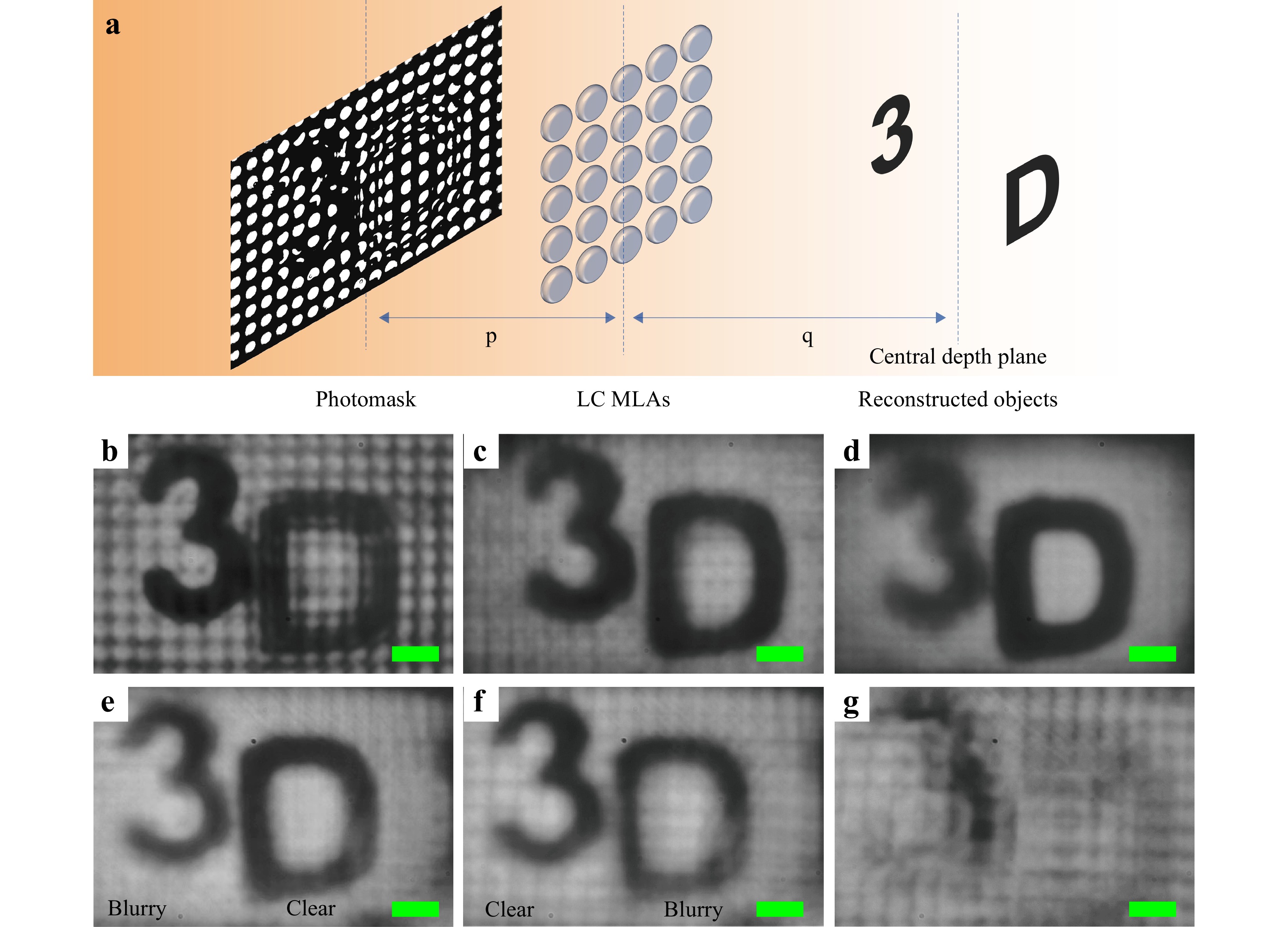
Microlenses or arrays are key elements in many applications. However, their construction methods involve multiple fabrication processes, thereby increasing the complexity and cost of fabrication. In this study, we demonstrate an optically anisotropic, electrically tunable liquid crystal (LC) microlens array using a simple, one-step fabrication method. The microlens array is formed via photopolymerization-induced phase separation inside a polymer/LC composite. It possesses both polarization-dependent and electrically tunable focusing and imaging properties. Without applying voltage, the microlens array has a natural focal length of 8 mm, which is a result of its inherent gradient refractive index profile. Upon applying voltage above the threshold, the LC molecules reorient along the electric field direction and the focal length of the microlens array gradually increases. Based on its superior properties, the microlens array is further used for integral imaging applications, demonstrating electrically tunable central depth plane. Such LC microlens arrays could find numerous potential applications owing to their advantageous features of being flat, ultra-thin, and tunable, including 3D displays, optical interconnects, and more.
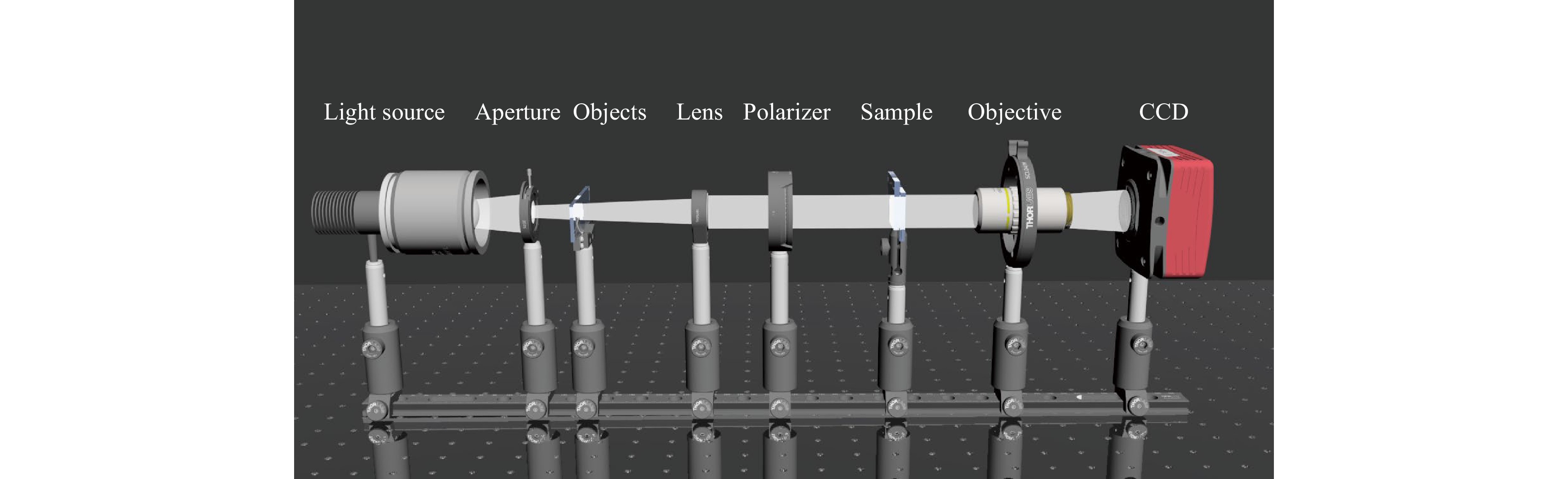
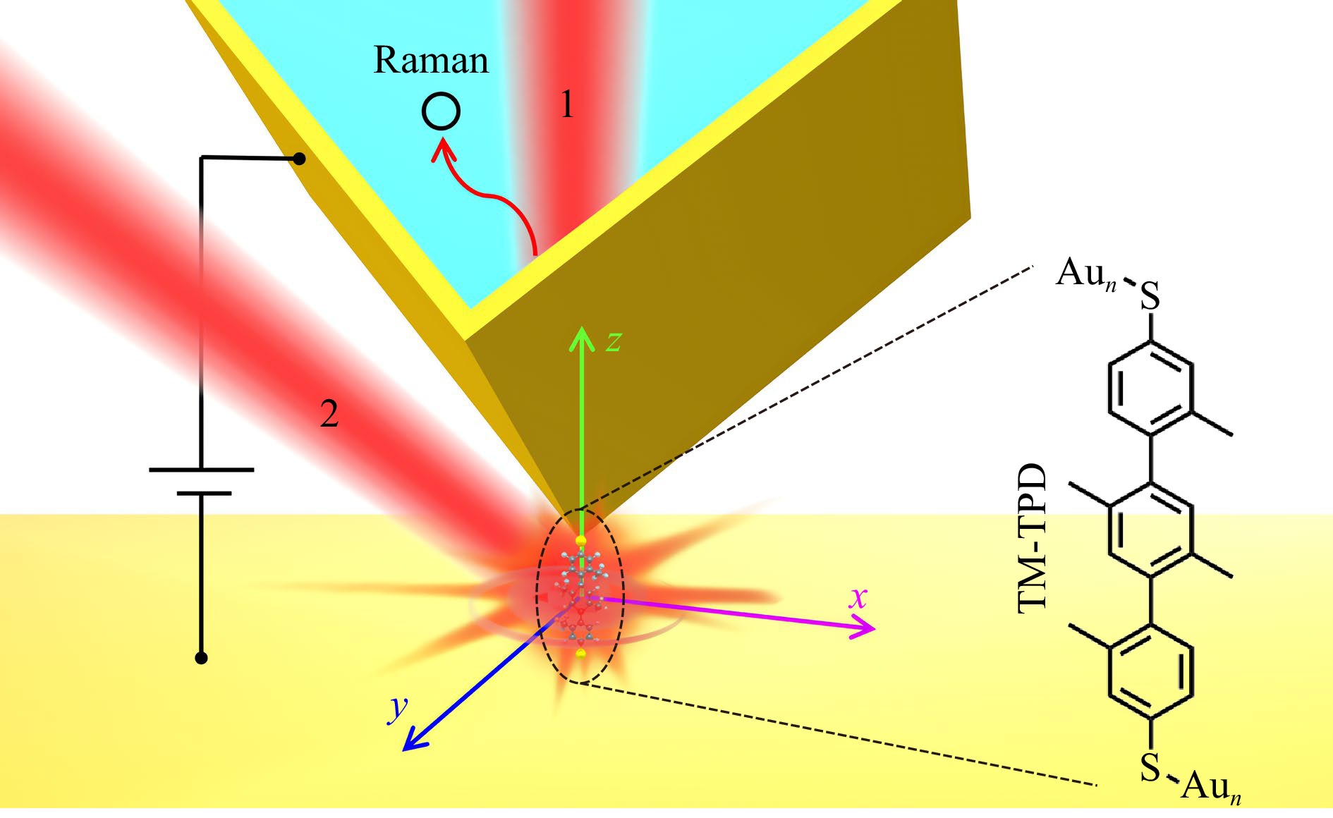
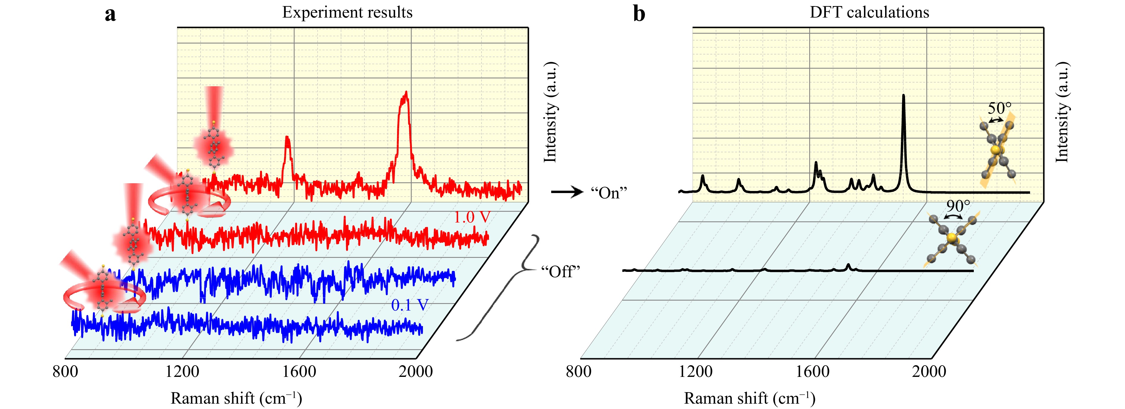
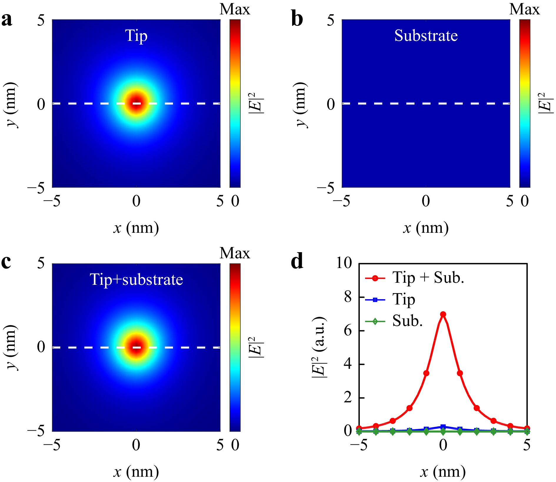
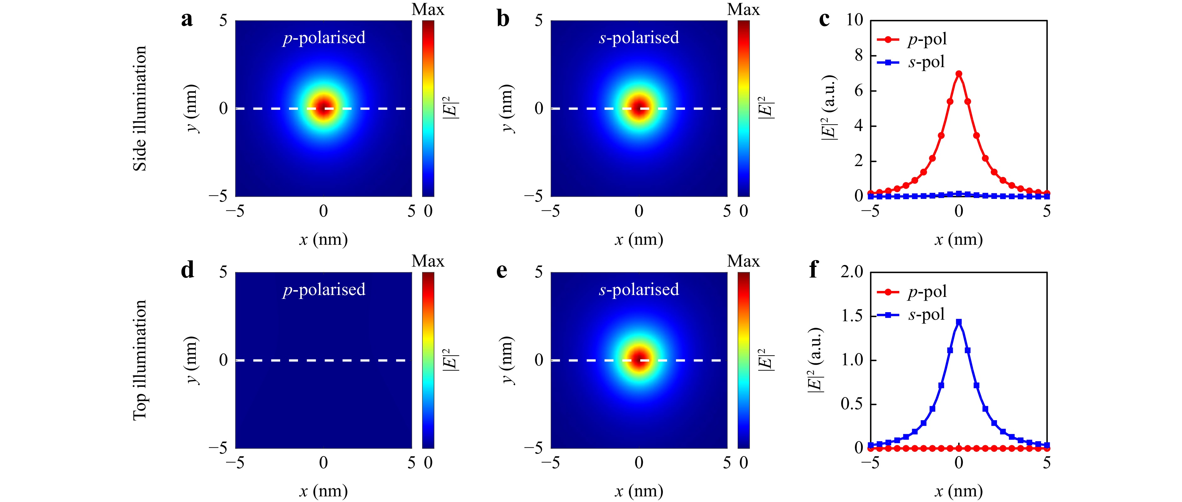
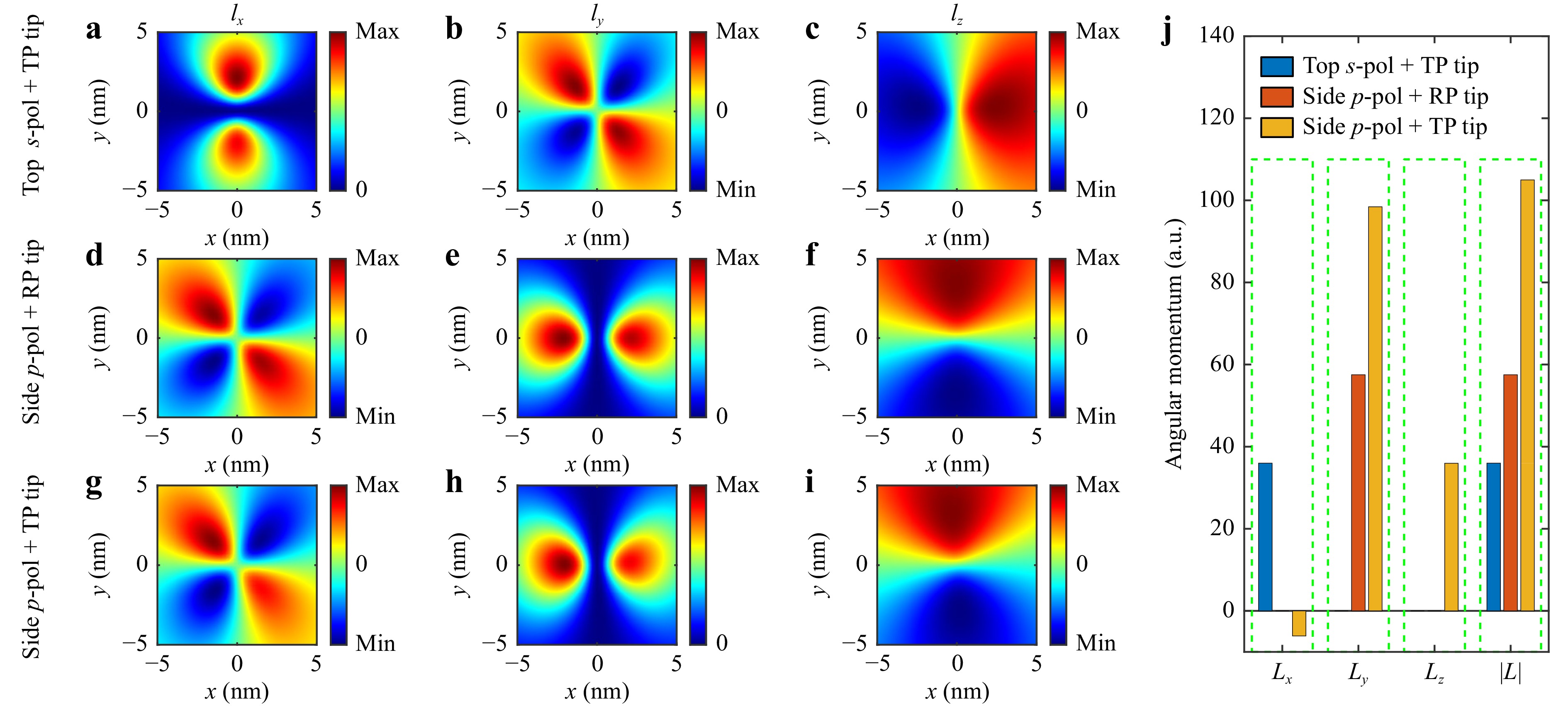
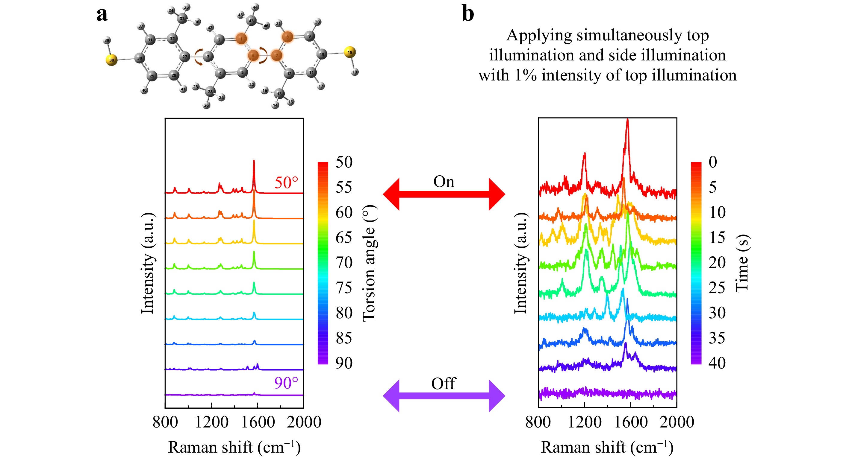
The role of molecular junctions in nanoelectronics is most often associated with electronic transport; however, their precise characterisation hinders their widespread development. The interaction of light with molecular junctions is a supplementary factor for the development of molecular switches, but it has rarely been addressed. The influence of light interaction with molecular junctions on the response of molecules in the near field was demonstrated by properly characterising the optical angular momentum at the junctions. Consequently, the molecular switching dynamics were observed in the Raman signatures of the conducting molecules. The illumination geometry and voltage applied to the junction were changed to demonstrate numerically and experimentally how the Raman intensity can be turned ON and OFF with a difference of nearly five orders of magnitude. These molecular-scale operations result from the combined interaction of a current-induced electronic rearrangement in the molecular junction and a plasmonically enhanced electromagnetic field near the tip of the junction. This study of the effect of optical angular momentum on the near field of the molecular junction shows significant potential for the development of molecular electronics.
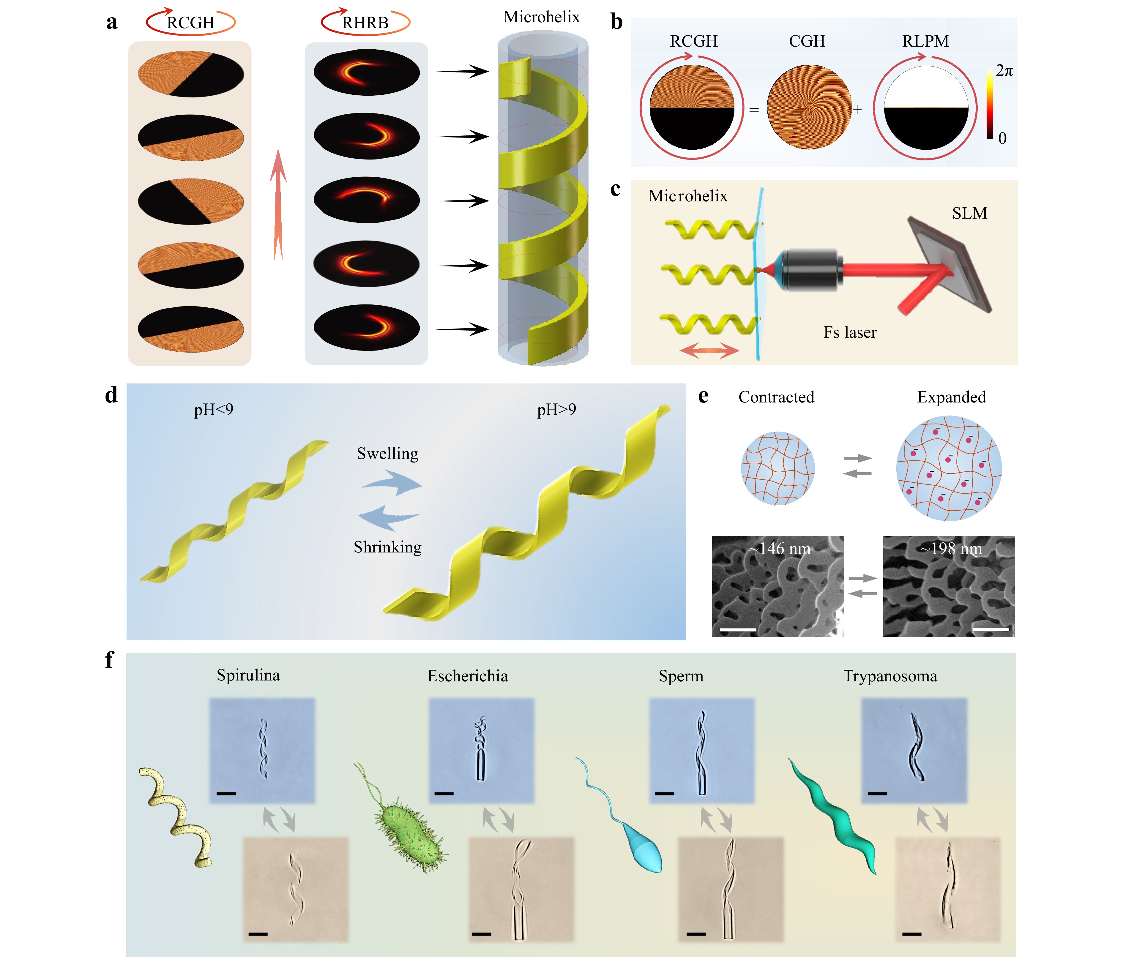
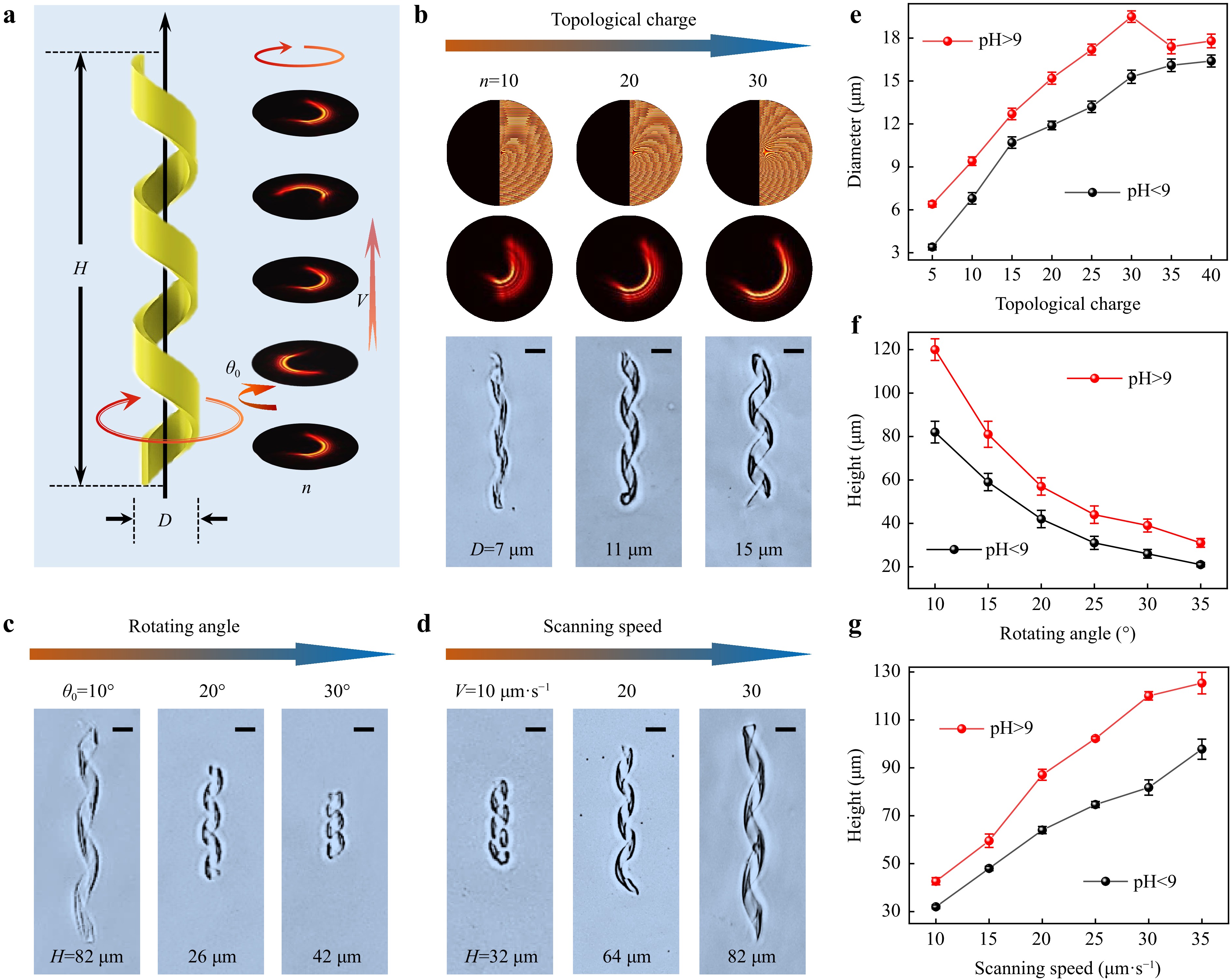
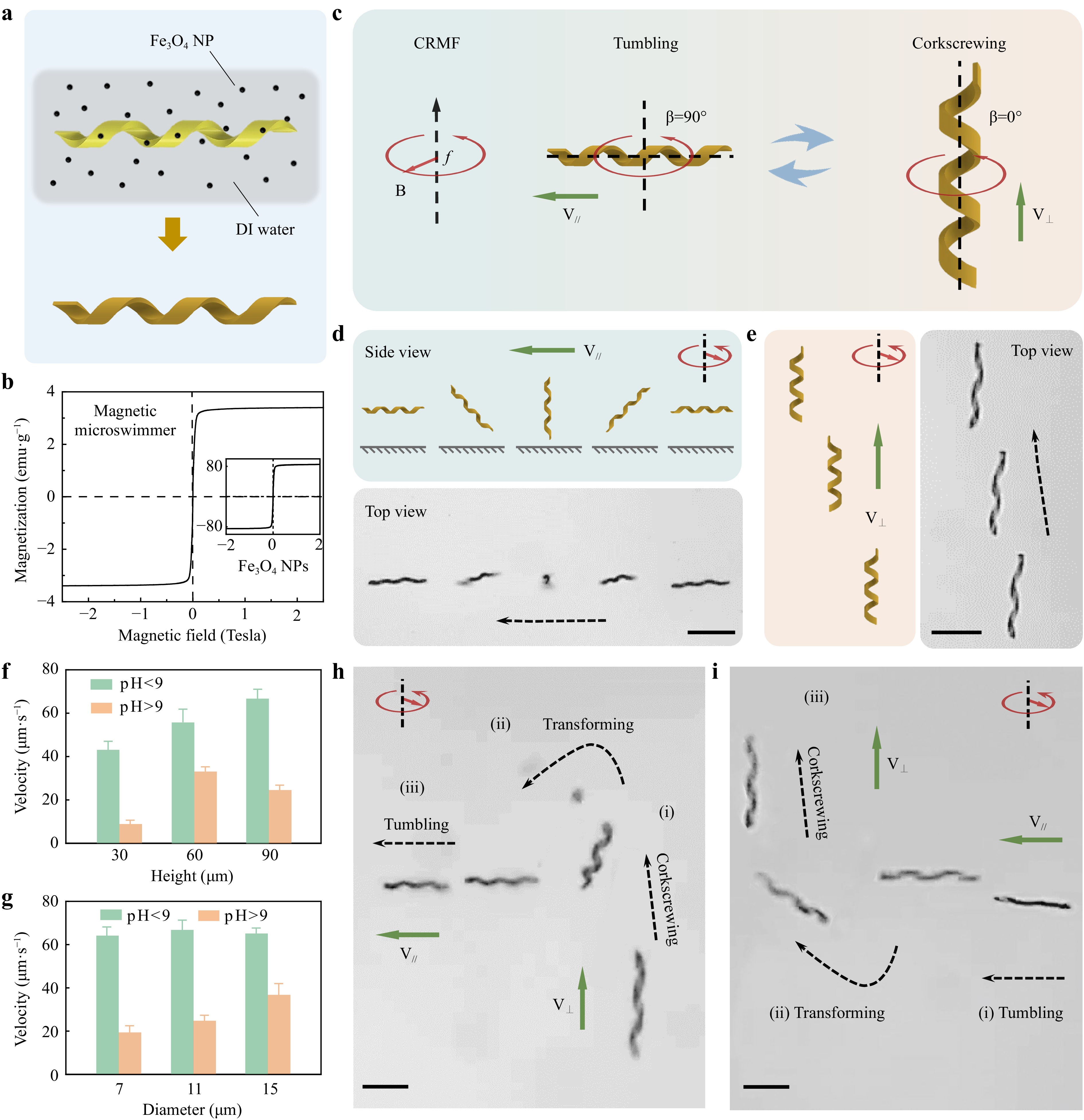
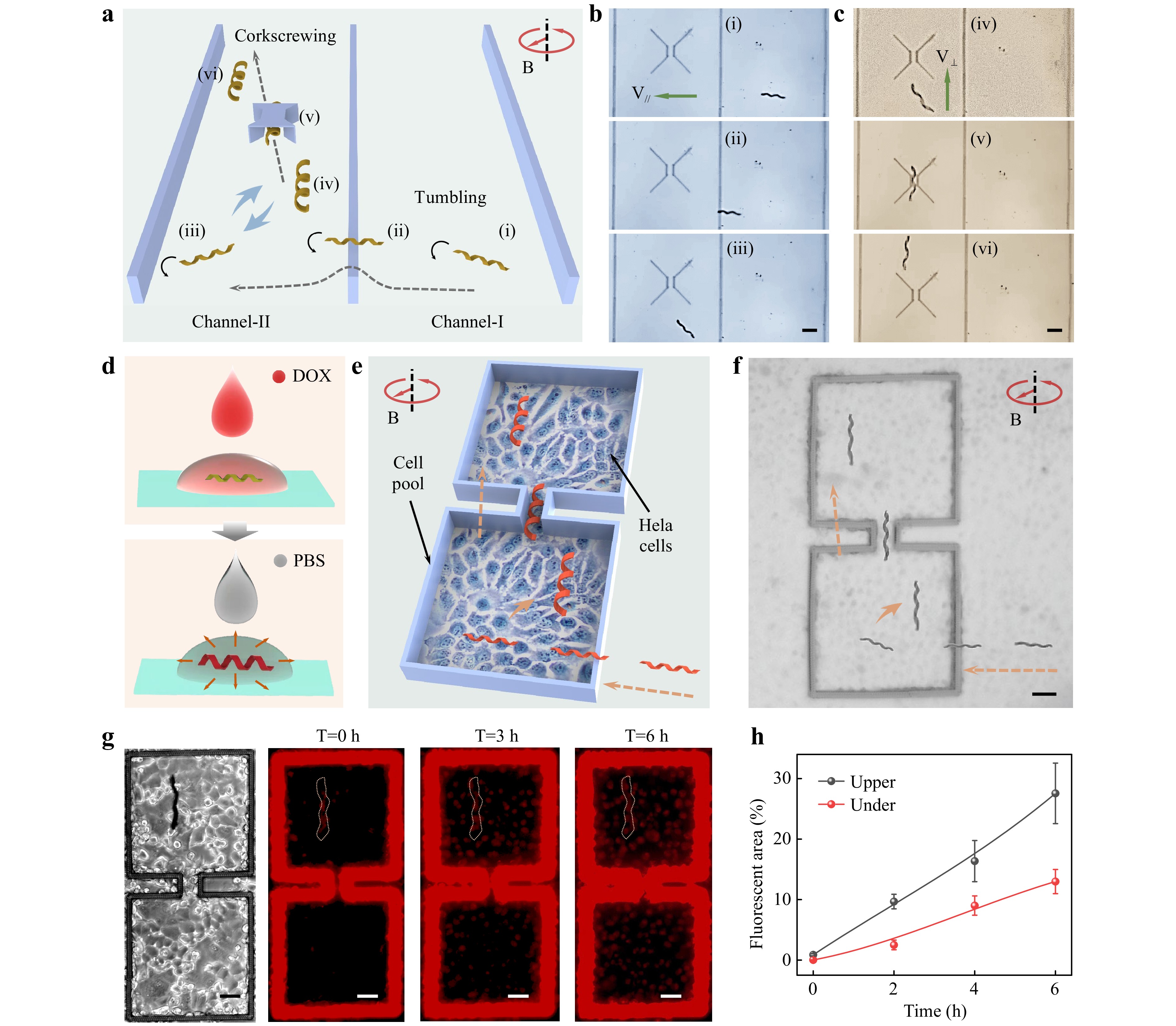
Artificial helical microswimmers with shape-morphing capacities and adaptive locomotion have great potential for precision medicine and noninvasive surgery. However, current reconfigurable helical microswimmers are hampered by their low-throughput fabrication and limited adaptive locomotion. Here, a rotary holographic processing strategy (a helical femtosecond laser beam) is proposed to produce stimuli-responsive helical microswimmers (<100 μm) rapidly (<1 s). This method allows for the easy one-step fabrication of various microswimmers with controllable sizes and diverse bioinspired morphologies, including spirulina-, Escherichia-, sperm-, and Trypanosoma-like shapes. Owing to their shape-morphing capability, the helical microswimmers undergo a dynamic transition between tumbling and corkscrewing motions under a constant rotating magnetic field. By exploiting adaptive locomotion, helical microswimmers can navigate complex terrain and achieve targeted drug delivery. Hence, these microswimmers hold considerable promise for diverse precision treatments and biomedical applications.
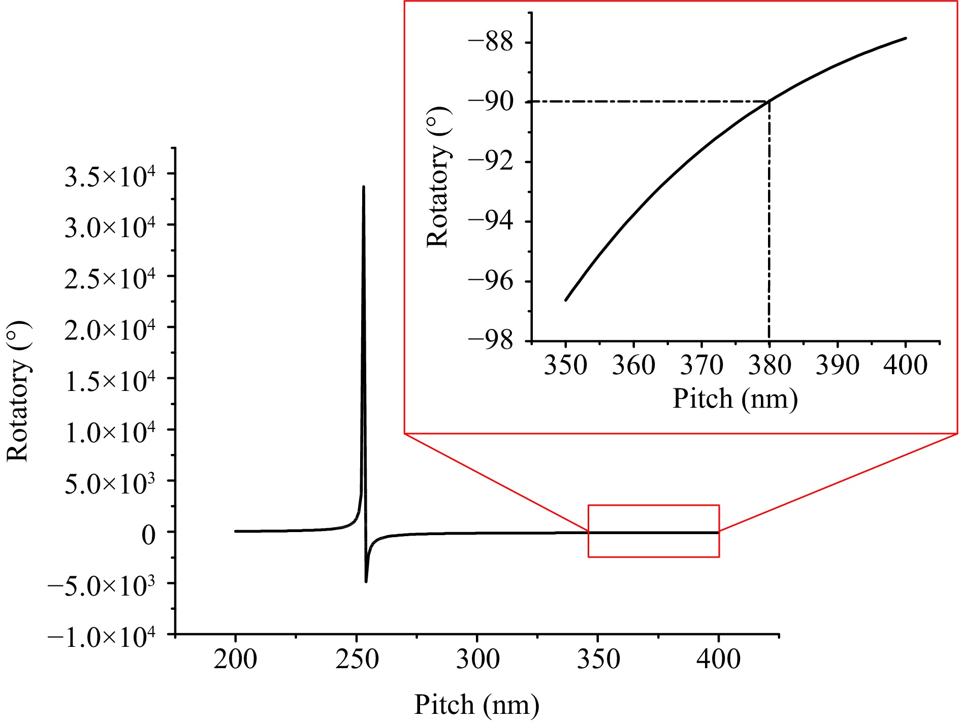
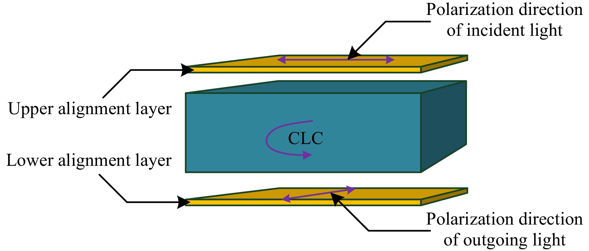
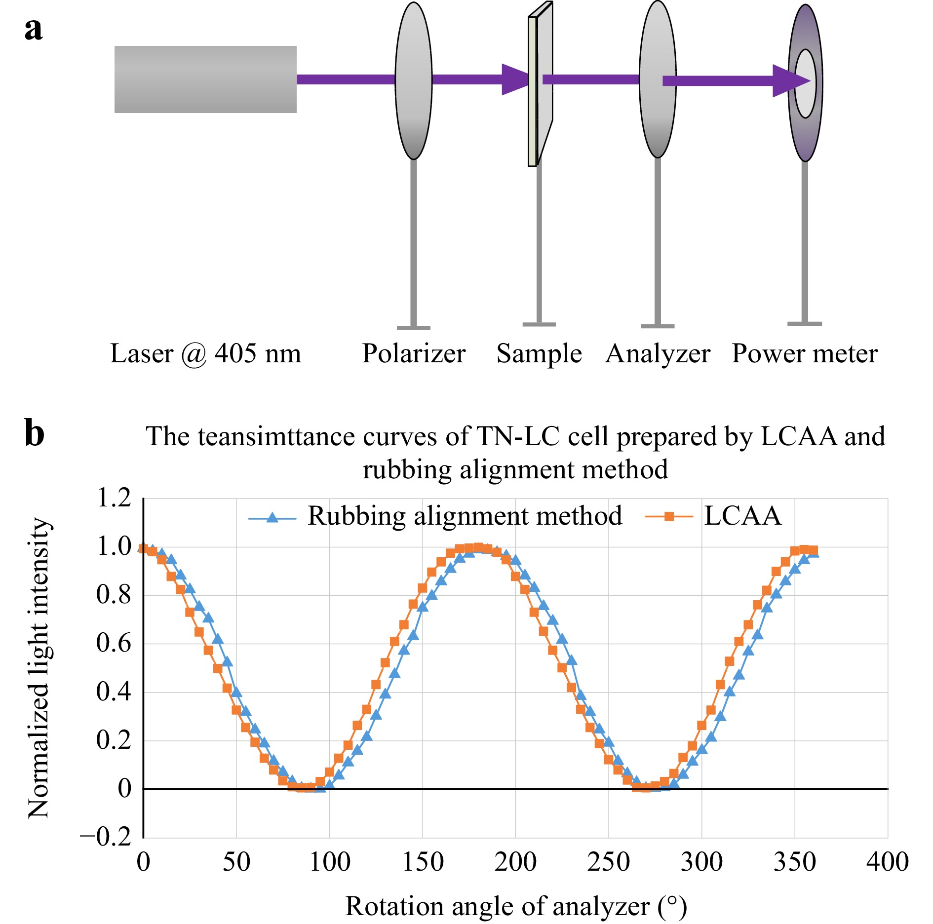
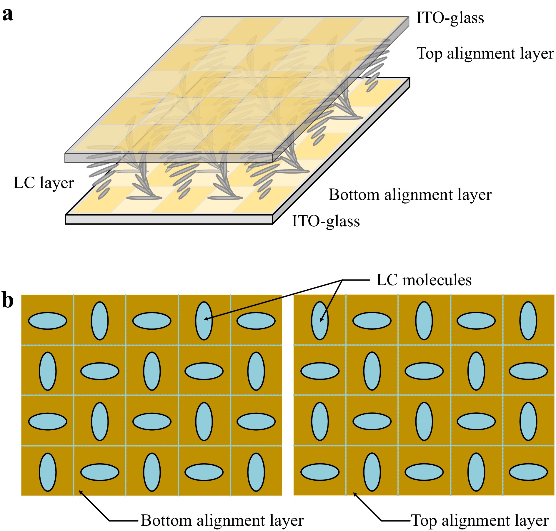
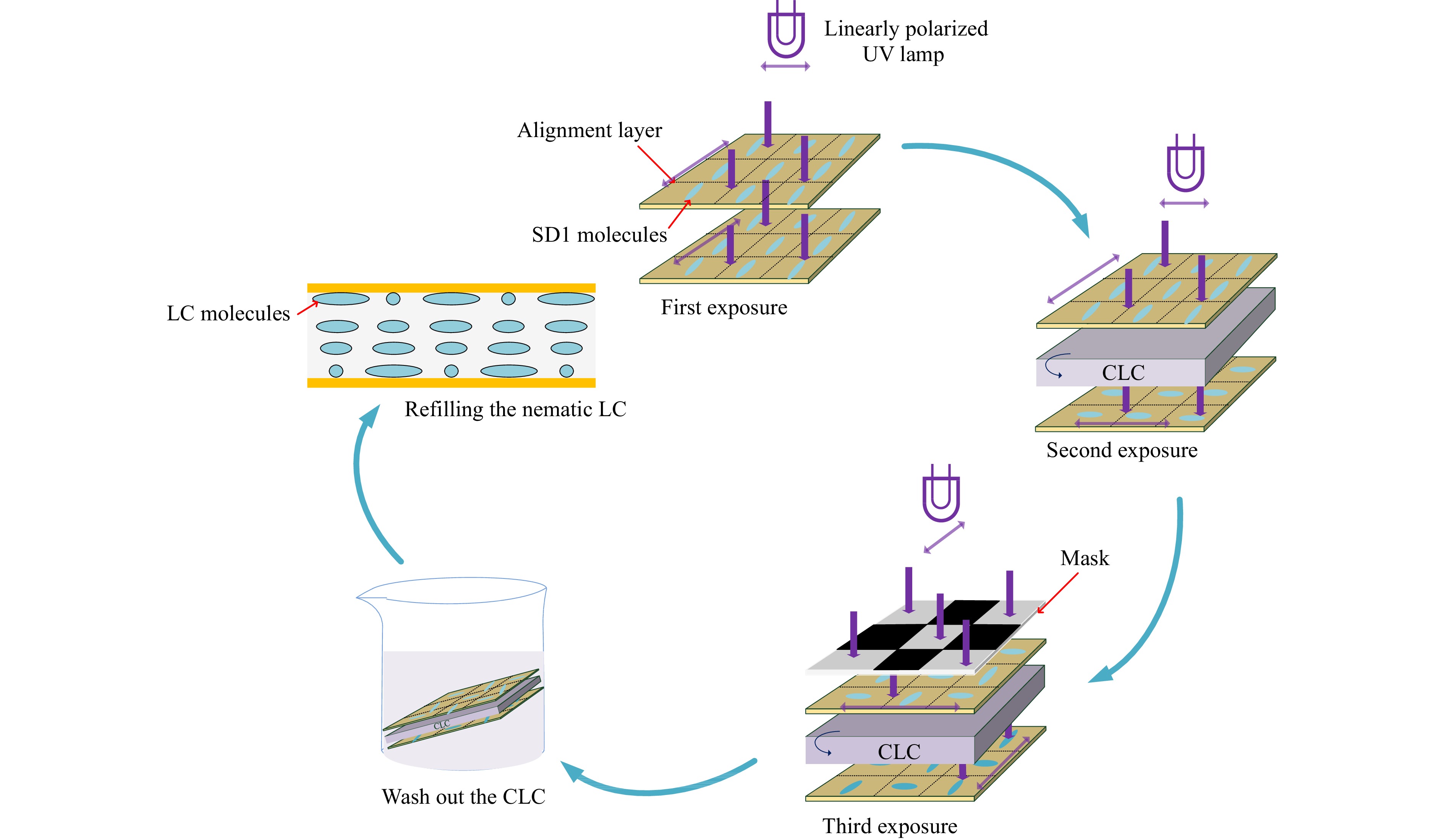
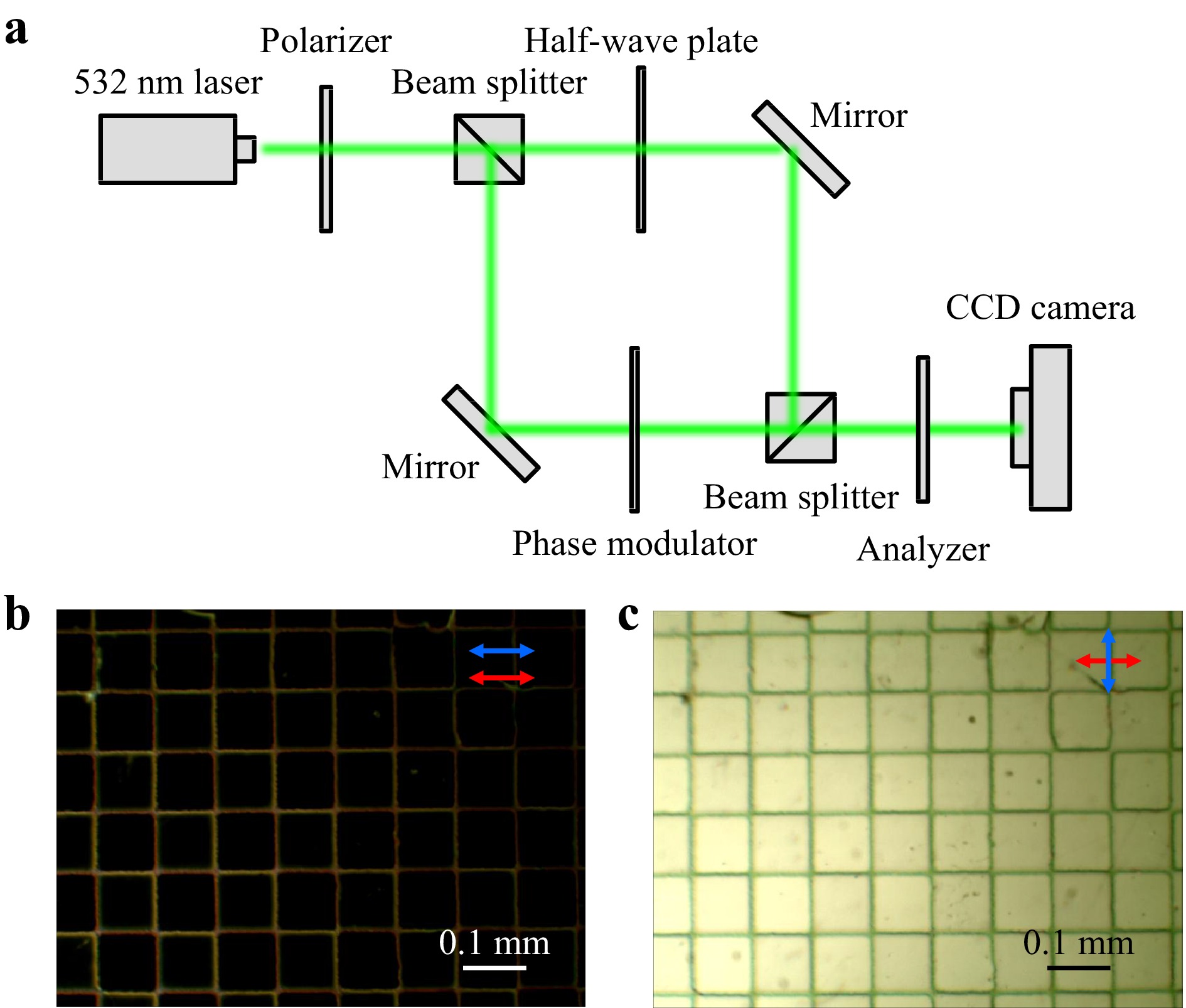
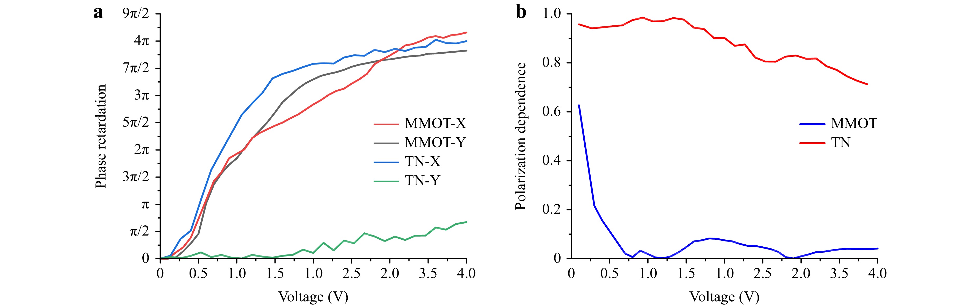
Polarization-independent liquid-crystal (LC) phase modulators can significantly improve the efficiency and reduce the complexity of optical systems. However, achieving good polarization independence for LC phase modulators with a simple structure is difficult. A light-controlled azimuth angle (LCAA) process based on the optical rotatory effect of cholesteric liquid crystals (CLC) was developed for fabricating single-layer, multi-microdomain, orthogonally twisted (MMOT) structures. The developed LC phase modulator with a single-layer MMOT structure may have a low polarization dependence with a large phase depth. This device shows good potential for applications in optical communications, wearable devices, and displays.
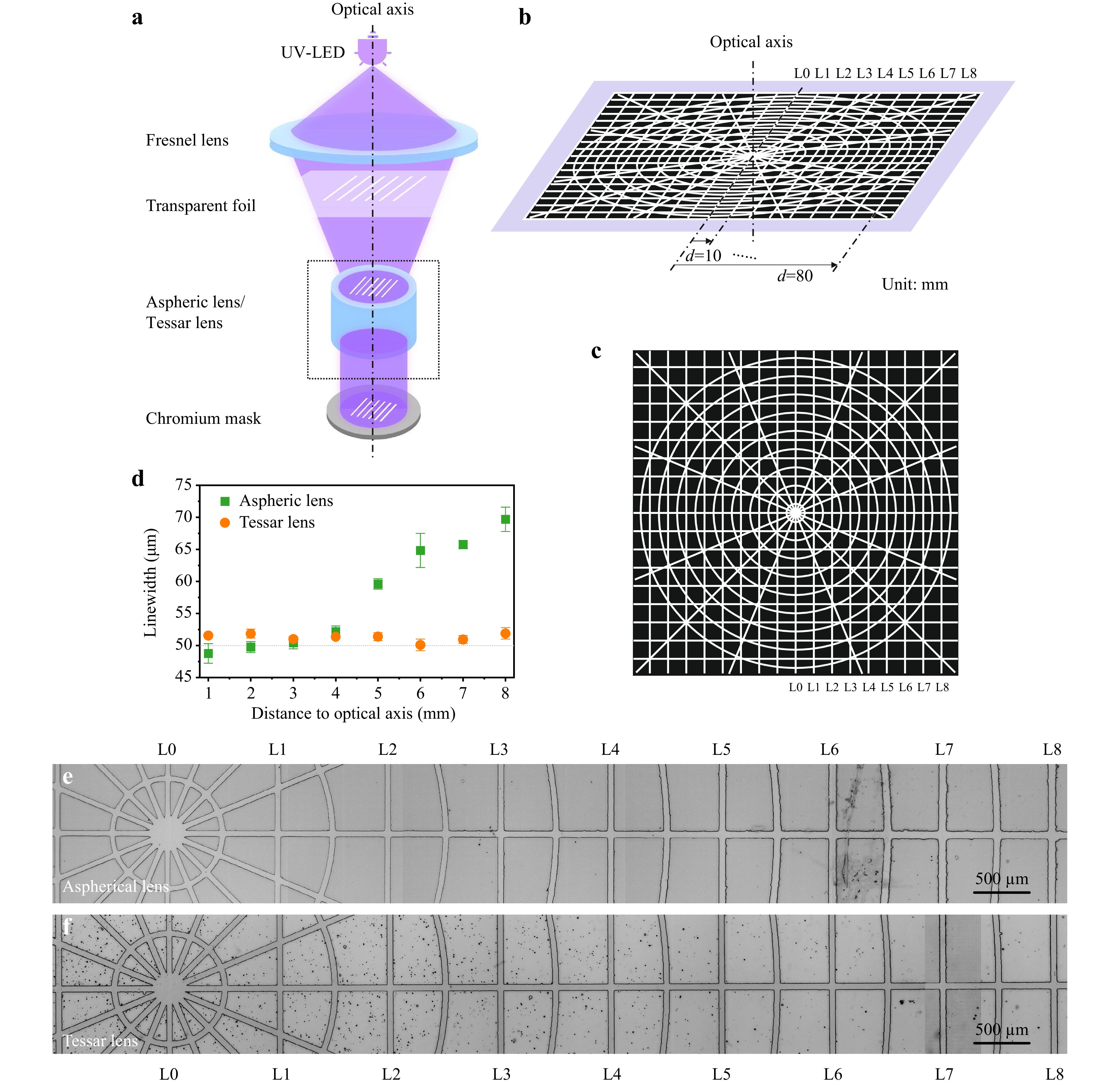
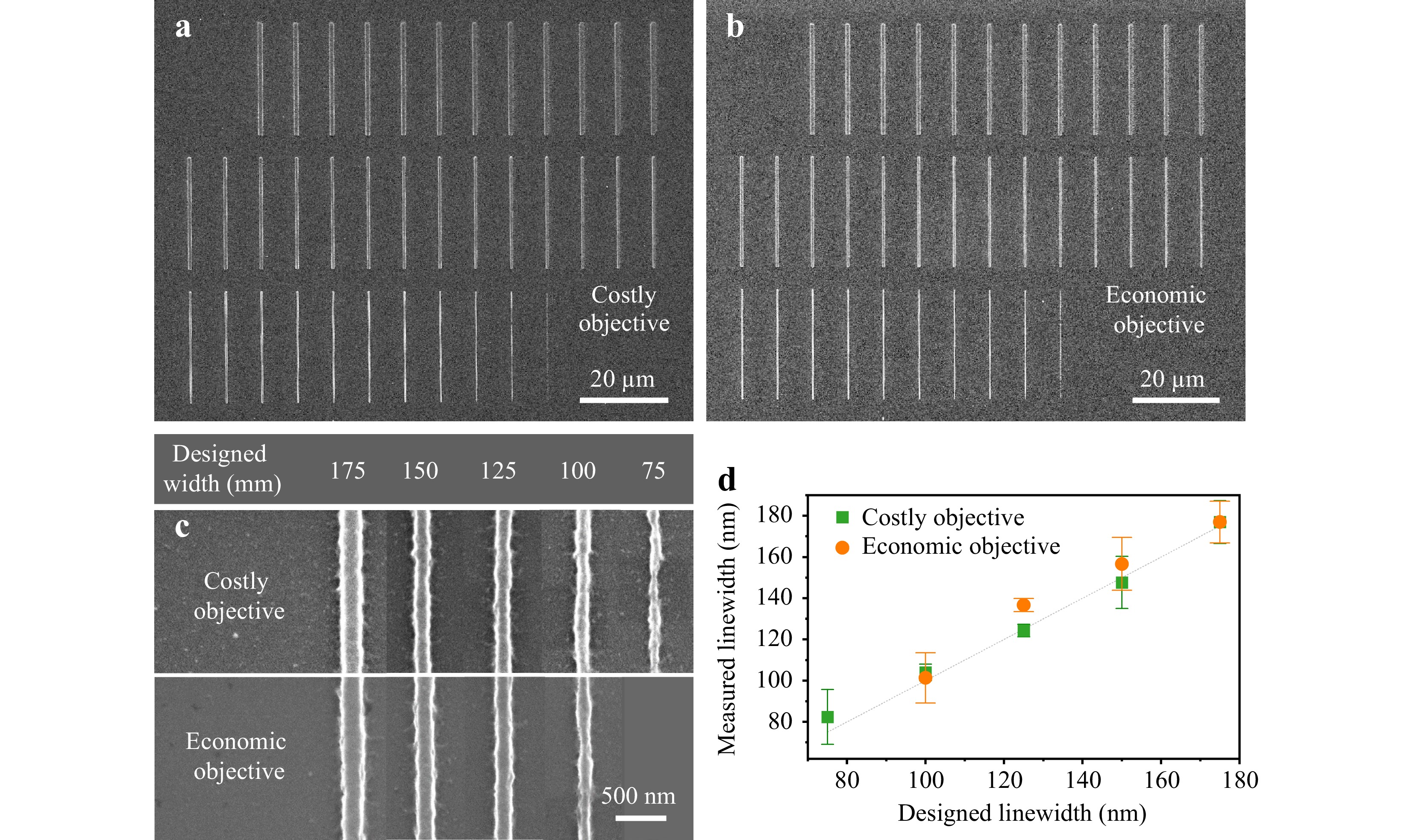
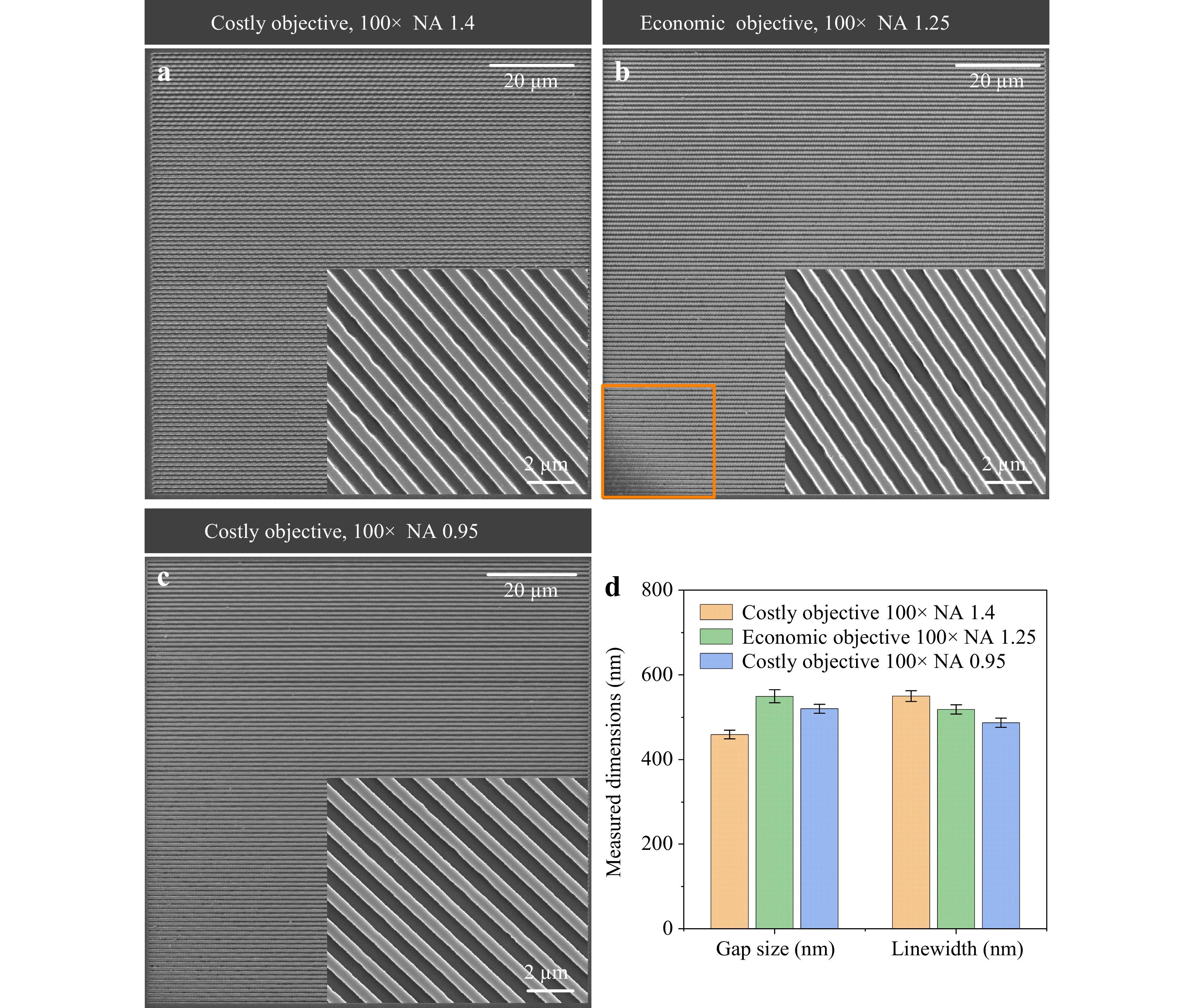
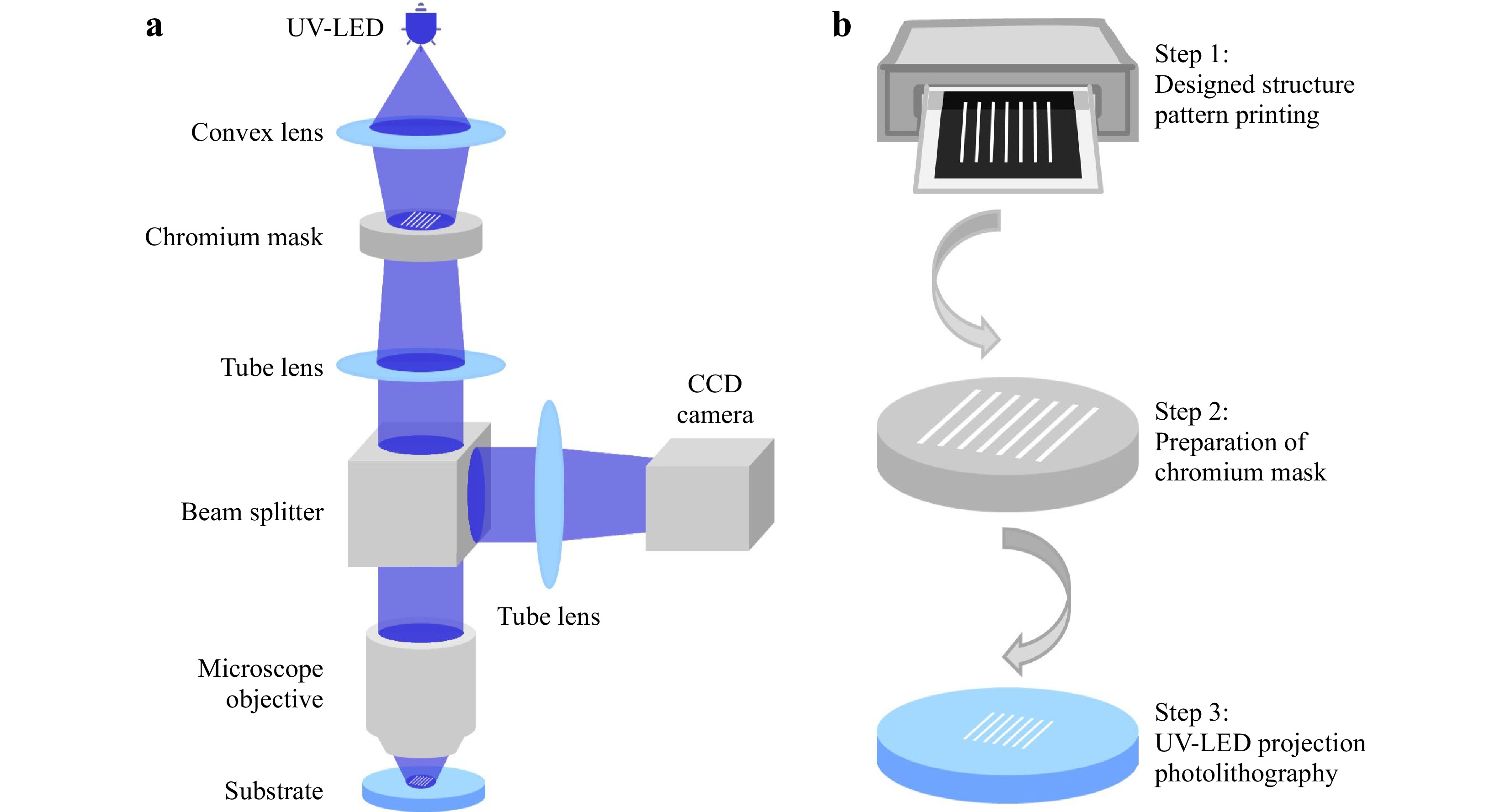
The demand for miniaturization and integration of optical elements has fostered the development of various micro- and nanofabrication technologies. In this work, we developed a low-cost UV-LED-based microscope projection photolithography system for rapid and high-resolution fabrication. This system can be easily implemented using off-the-shelf components. It allows for micro- and nanostructuring within seconds. By optimizing the process, a minimum feature size down to approximately 85 nm was successfully realized. In addition, investigations on fabrication of the same structures using both costly and economic microscope objectives were performed. Feature sizes below 100 nm can be stably achieved. The demonstrated approach extends the technology capabilities and may find applications in fields such as nanophotonics, biophotonics sensing and material science.
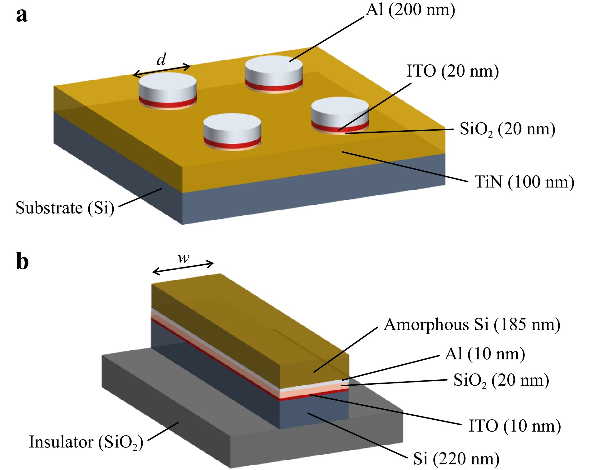
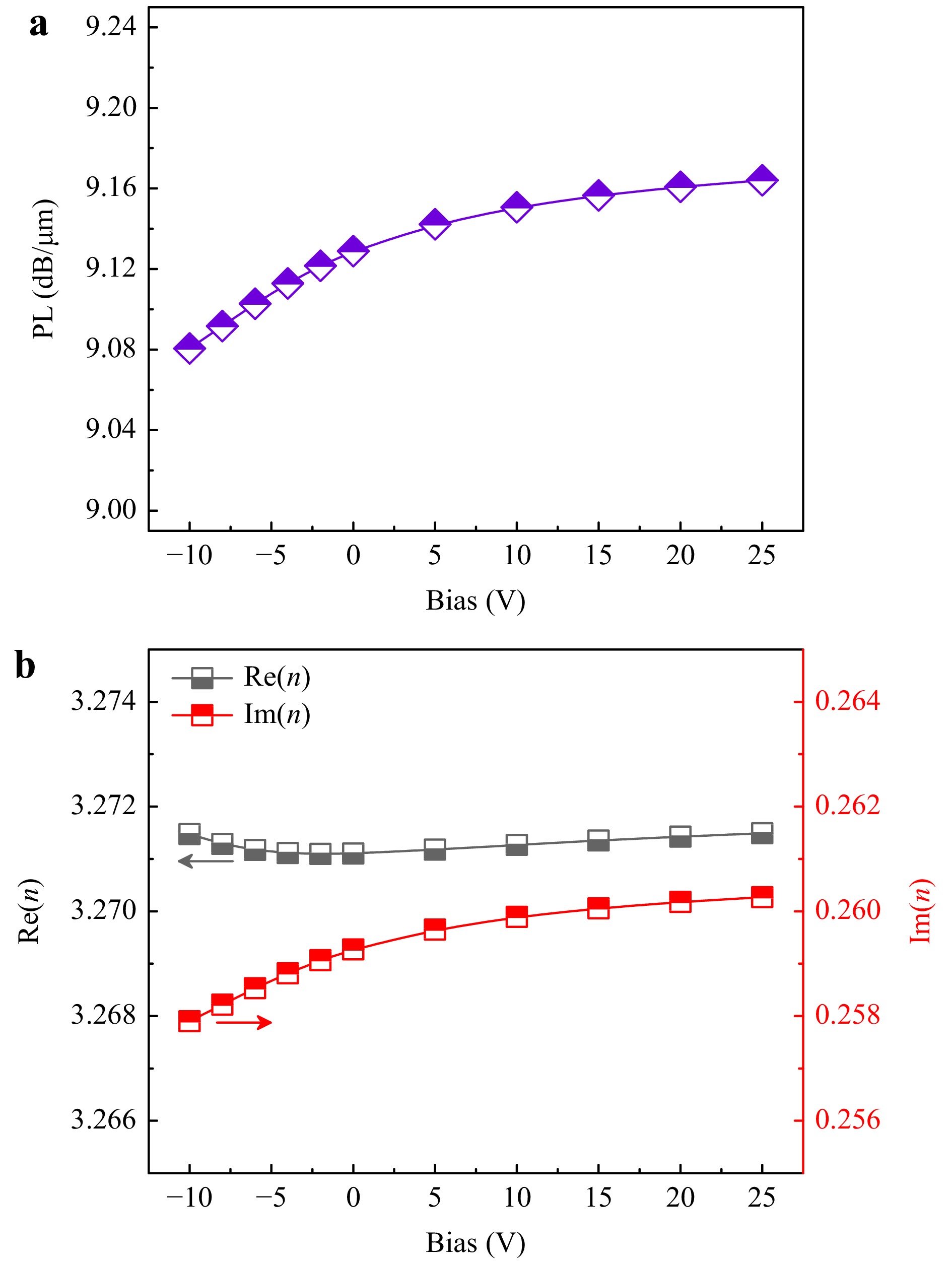
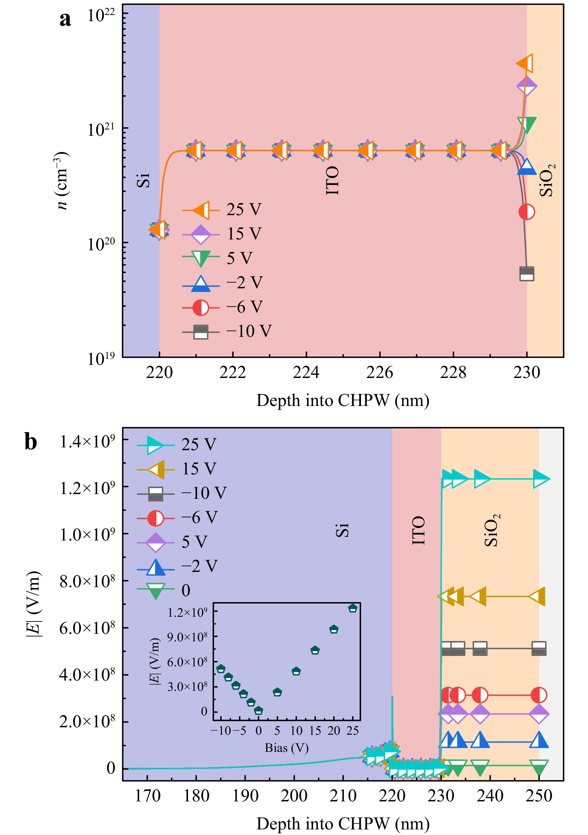
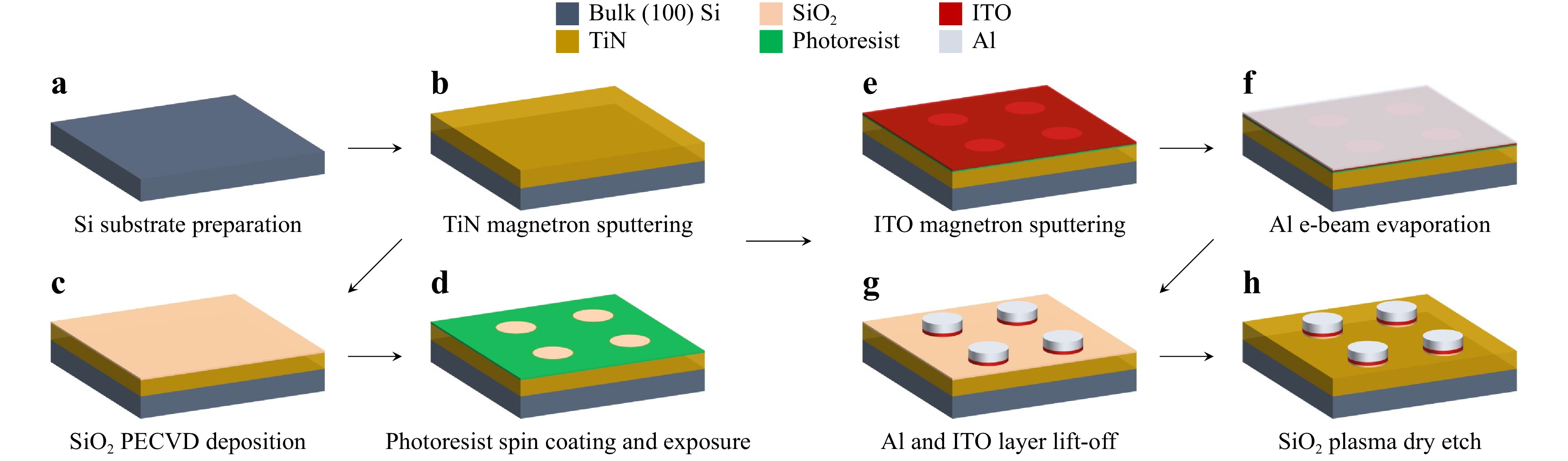
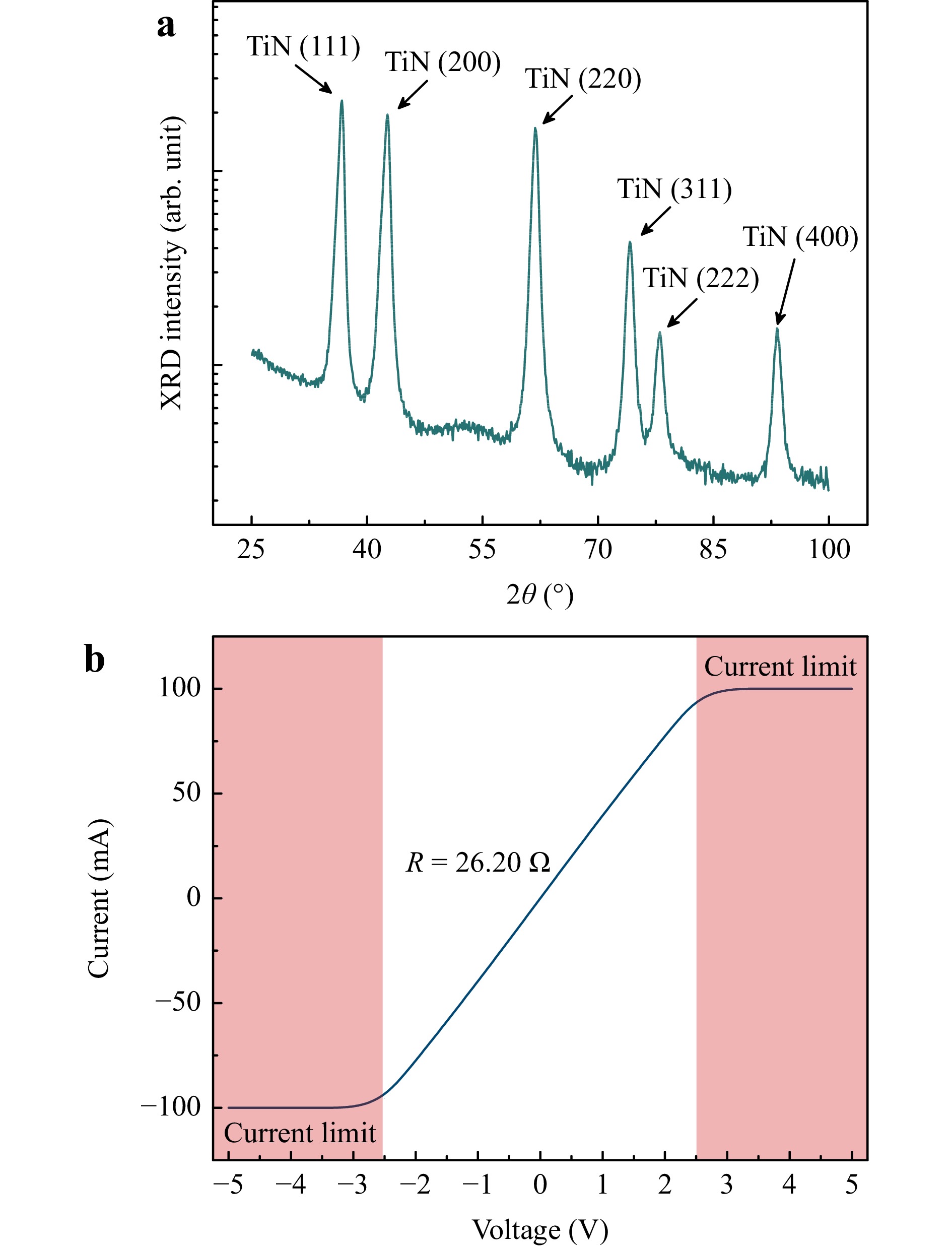
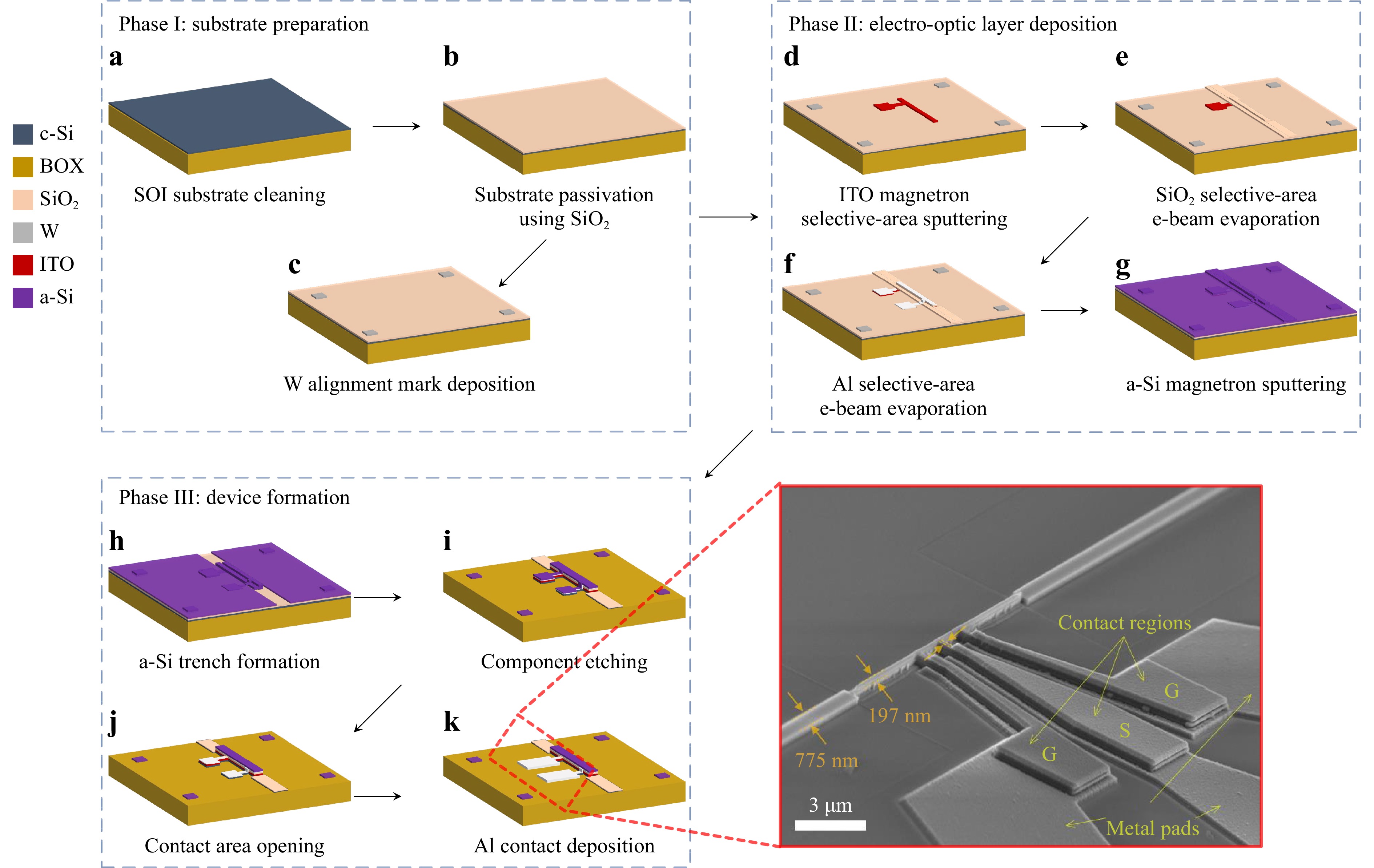
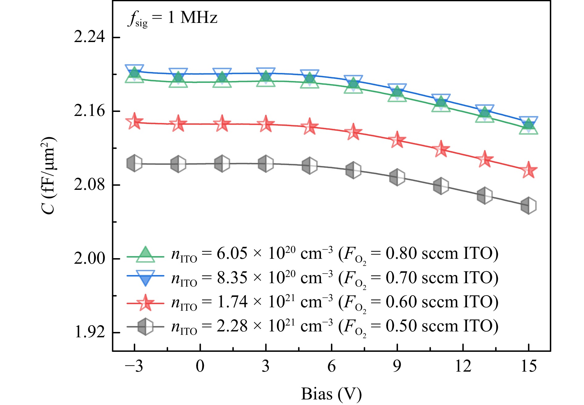
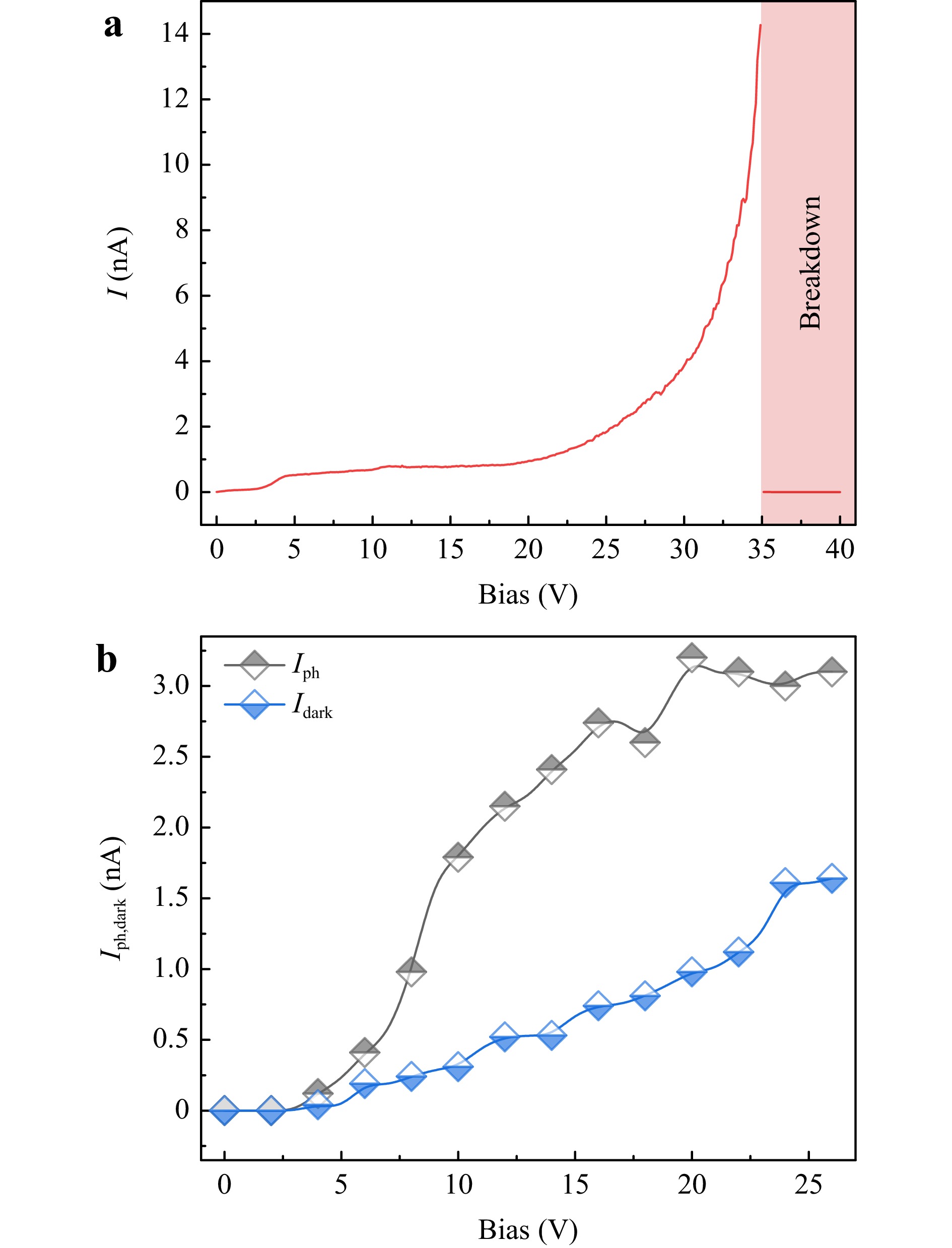
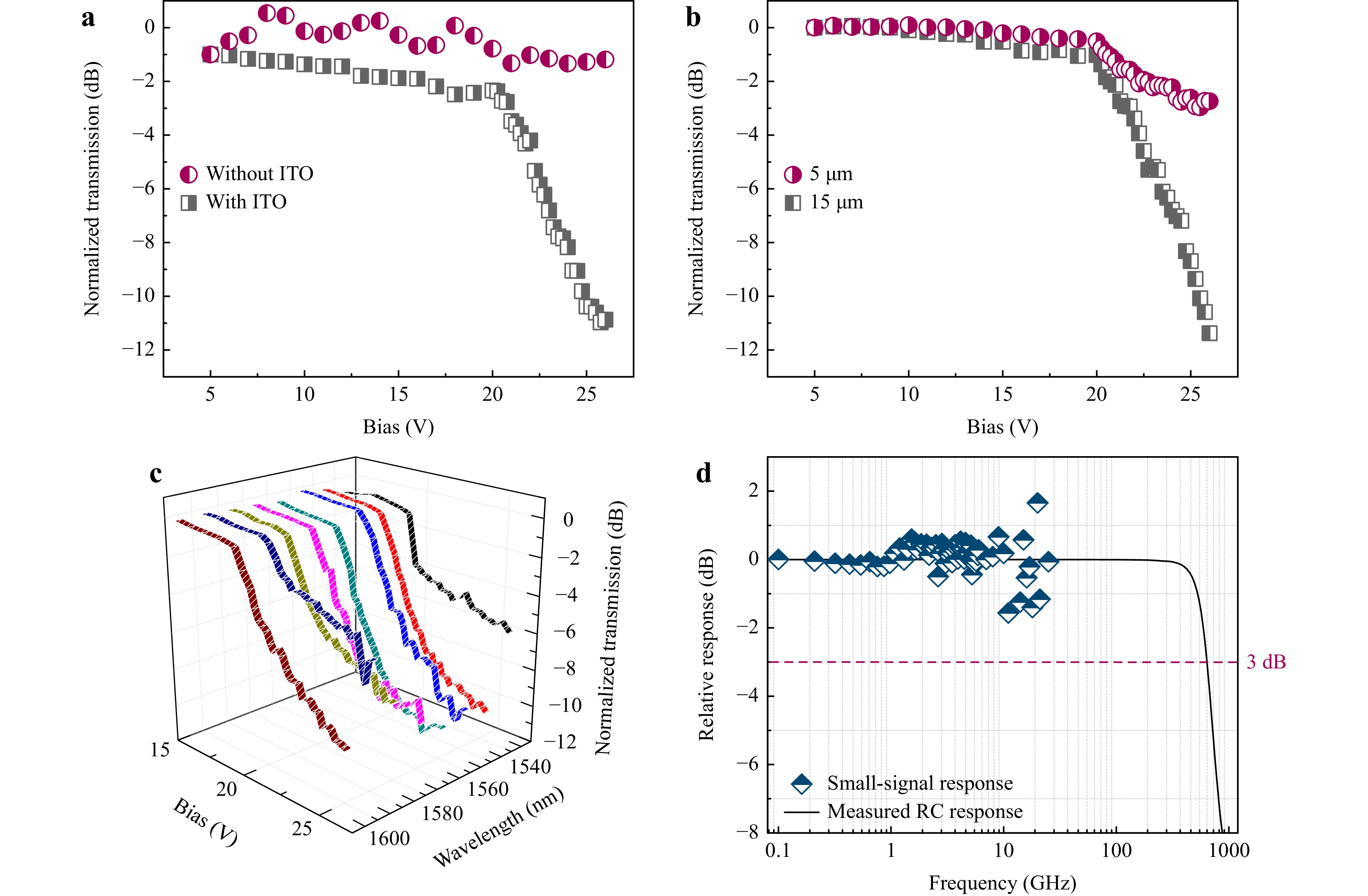
By taking advantage of the absence of diffraction limit restrictions in plasmonic structures, strong modal confinement is made possible, paving the way for improved optical processes and miniaturized photonic circuit integration. Indium tin oxide (ITO) has emerged as a promising plasmonic material that serves as a relatively low-carrier density Drude metal by its electro-optic tunability and versatility as an integrative oxide. We herein demonstrate the facile integration of SiO2/ITO heterointerfaces into metal–insulator–semiconductor (MIS) electro-optic structures. The first MIS device employs a SiO2/ITO heterostructure grown on thin polycrystalline titanium nitride (poly-TiN) and capped at the ITO side with thin aluminum (Al) film contact electrode. The TiN interlayer acts as a bottom electrode, forming a metal–insulator–semiconductor-metal (MISM) heterojunction device, and grows directly on (100)-oriented silicon (Si). This MISM device enables one to examine the electrical properties of semiconductive ITO layers. The second MIS device incorporates a semiconductive ITO layer with a SiO2 dielectric spacer implemented on a silicon-on-insulator (SOI) platform, forming a graded-index coupled hybrid plasmonic waveguide (CHPW) modulator. This device architecture represents a crucial step towards realizing plasmonic modulation using oxide materials. The CHPW device performance presented herein provides a proof-of-concept that demonstrates the advantages offered by such device topology to perform optical modulation via charge carrier dispersion. The graded-index CHPW can be dynamically reconfigured for amplitude, phase, or 4-quadrature amplitude modulation utilizing a triode-like biasing strategy. It exhibited extinction ratio (ER) and insertion loss (IL) levels of around 1 dB/μm and 0.128 dB/μm, respectively, for a 10 μm waveguide length.
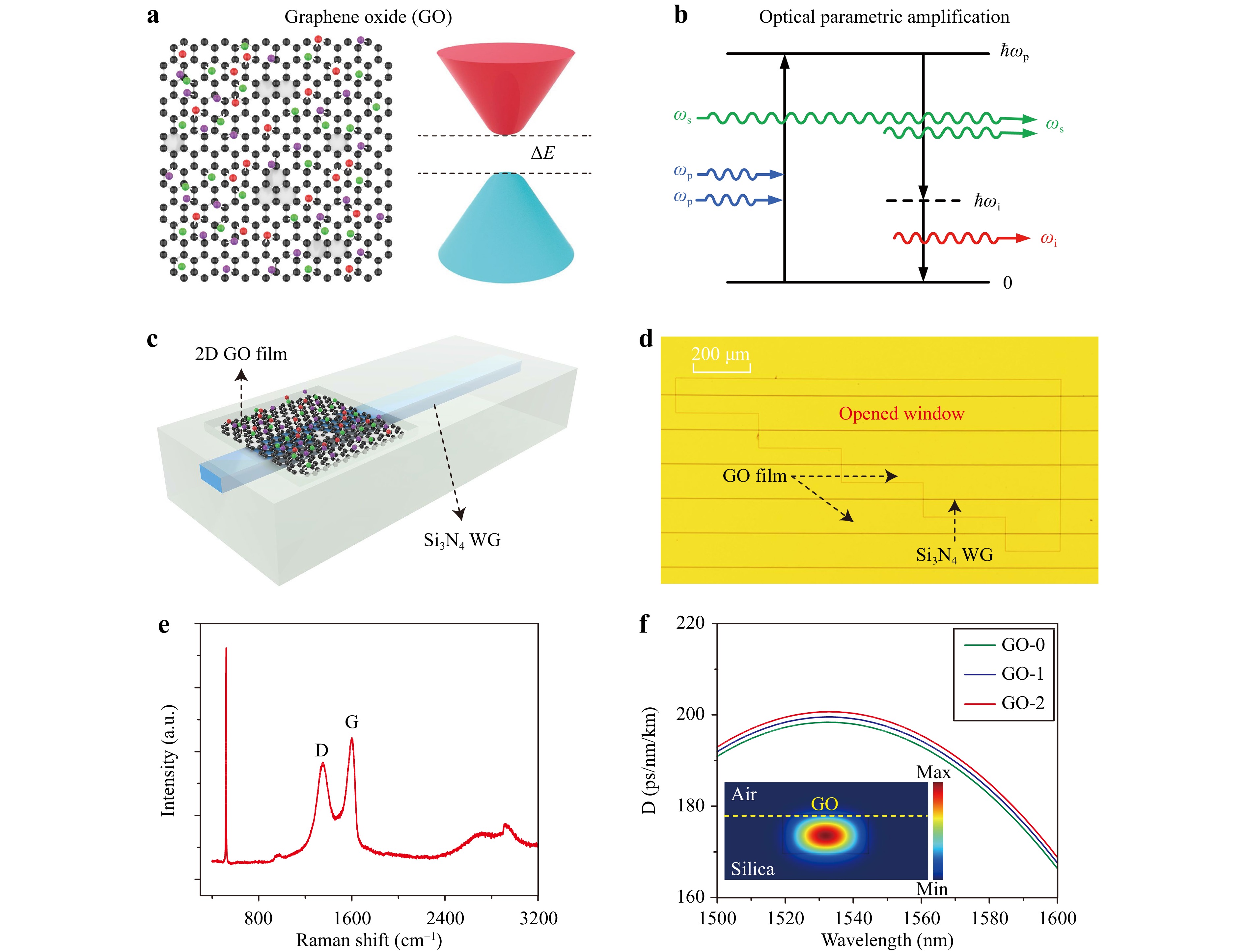
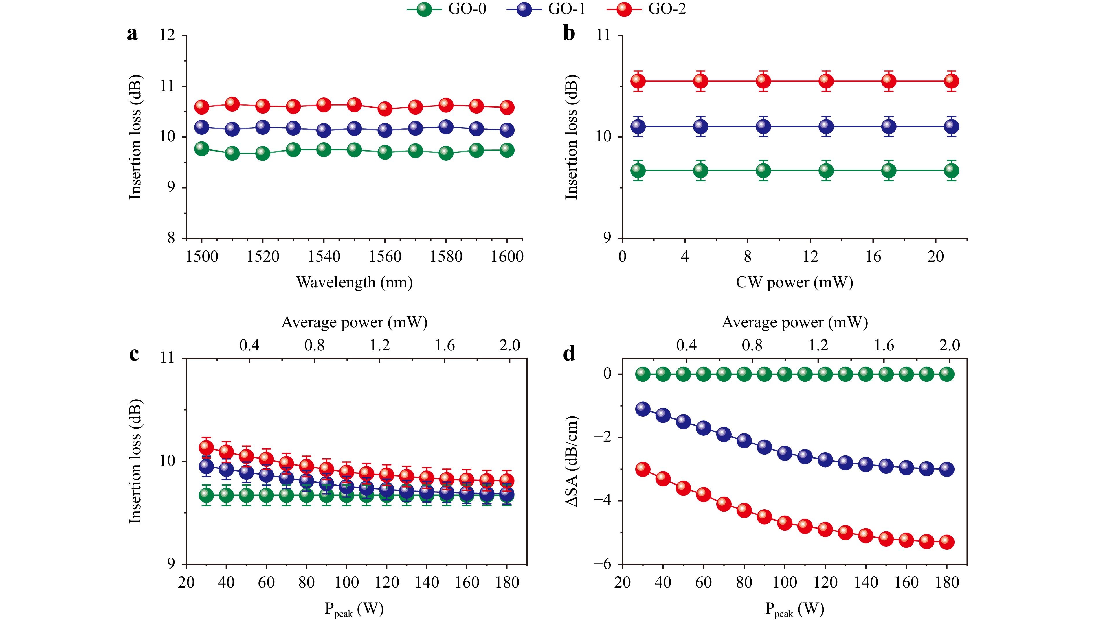
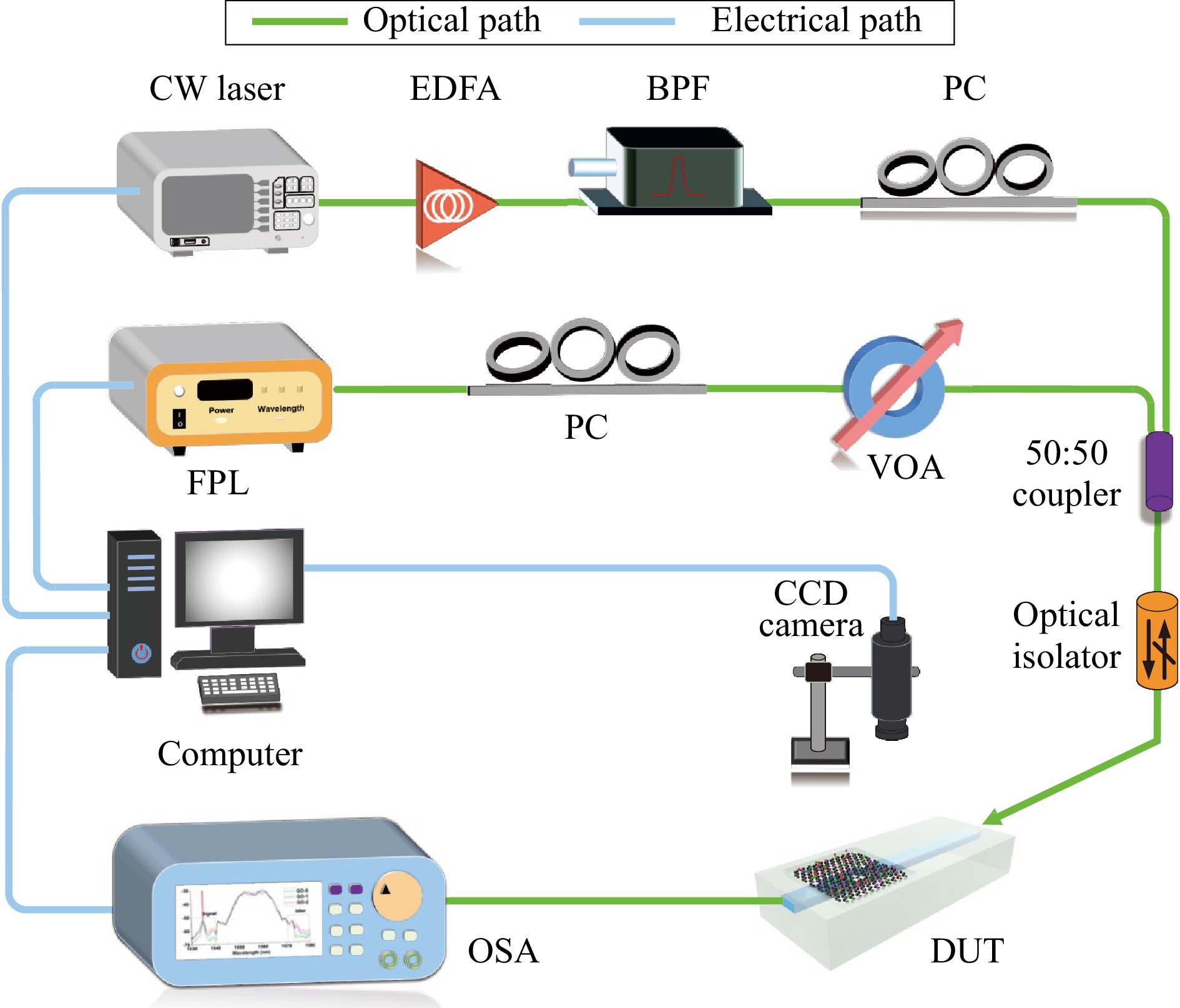
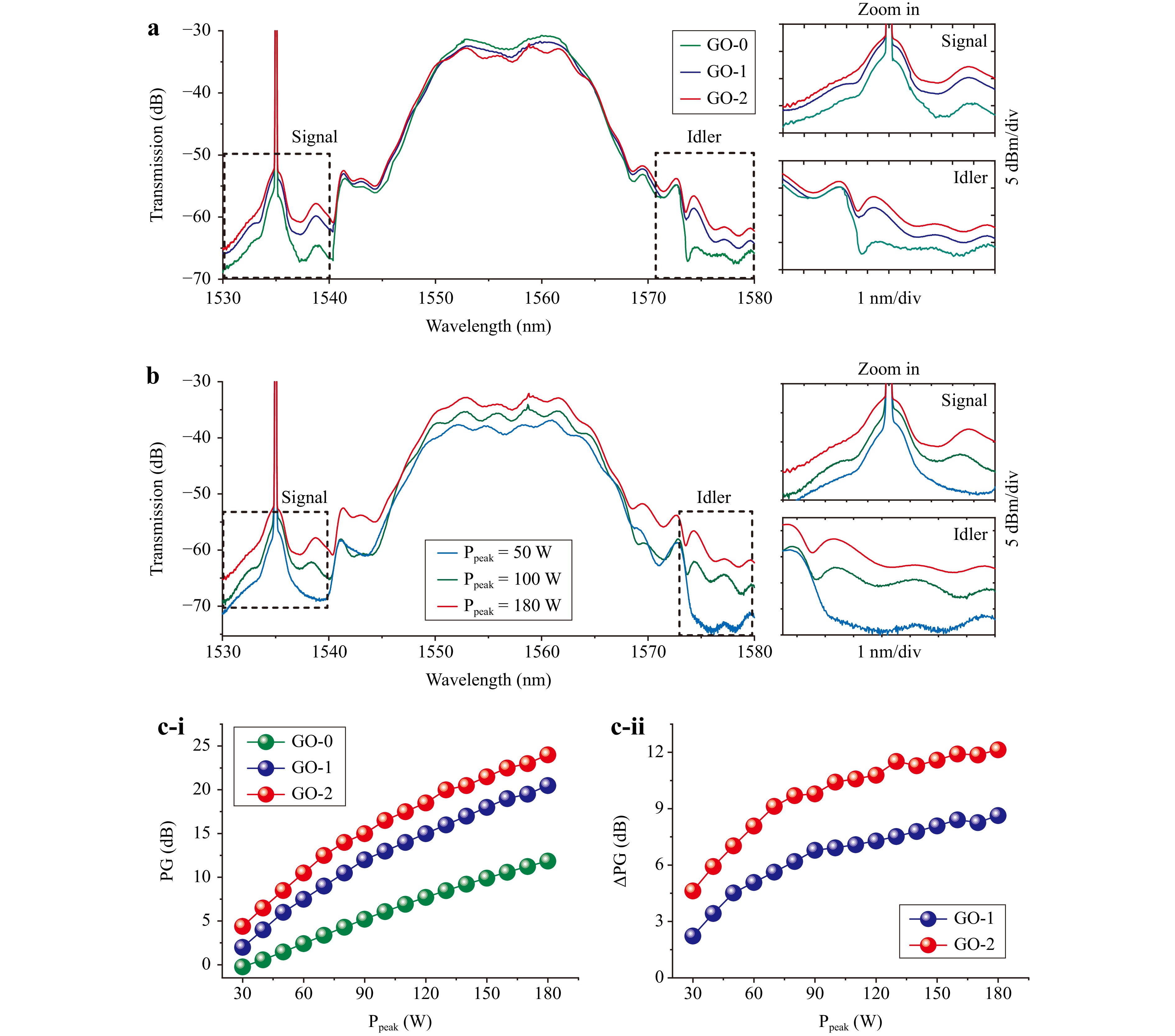
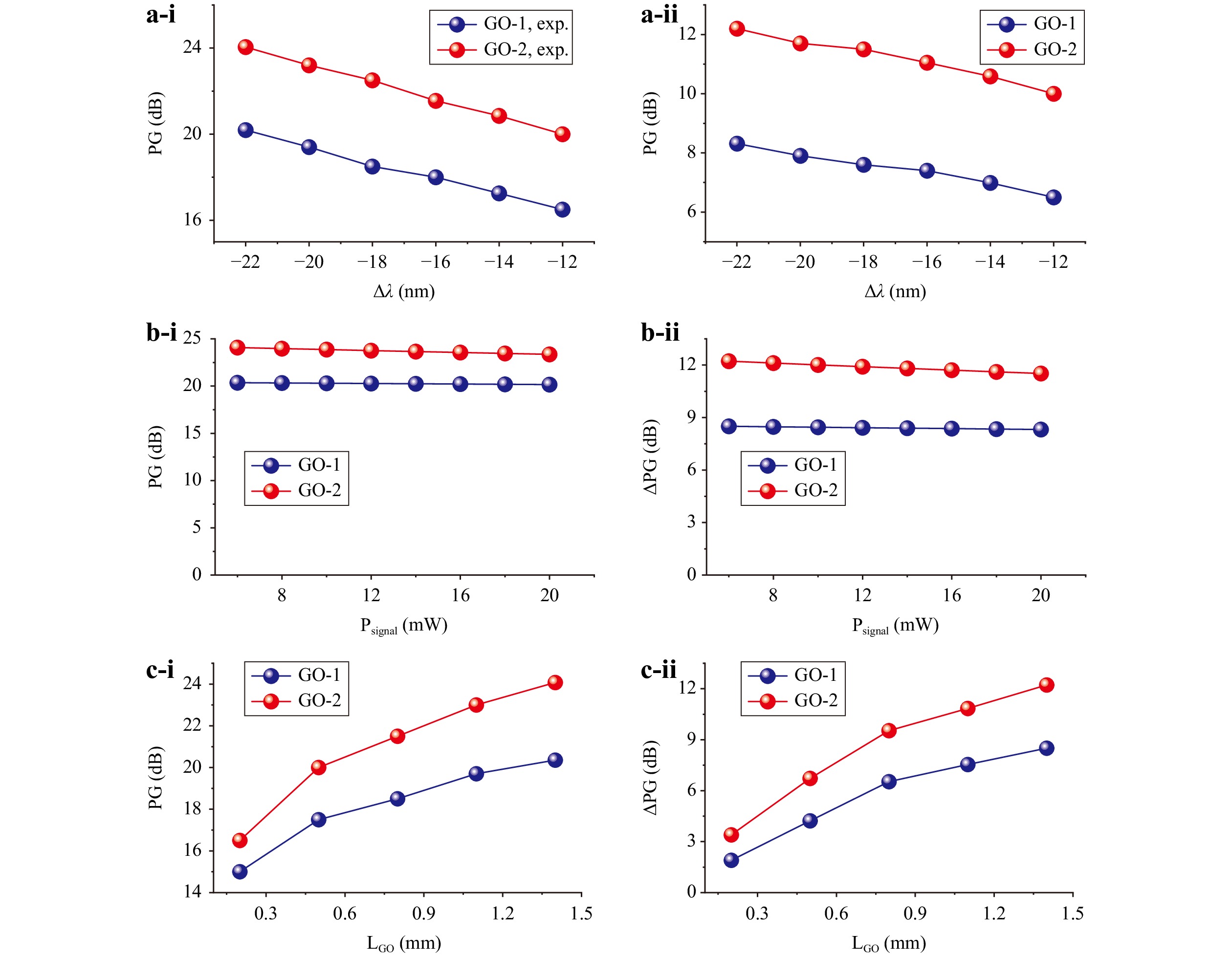
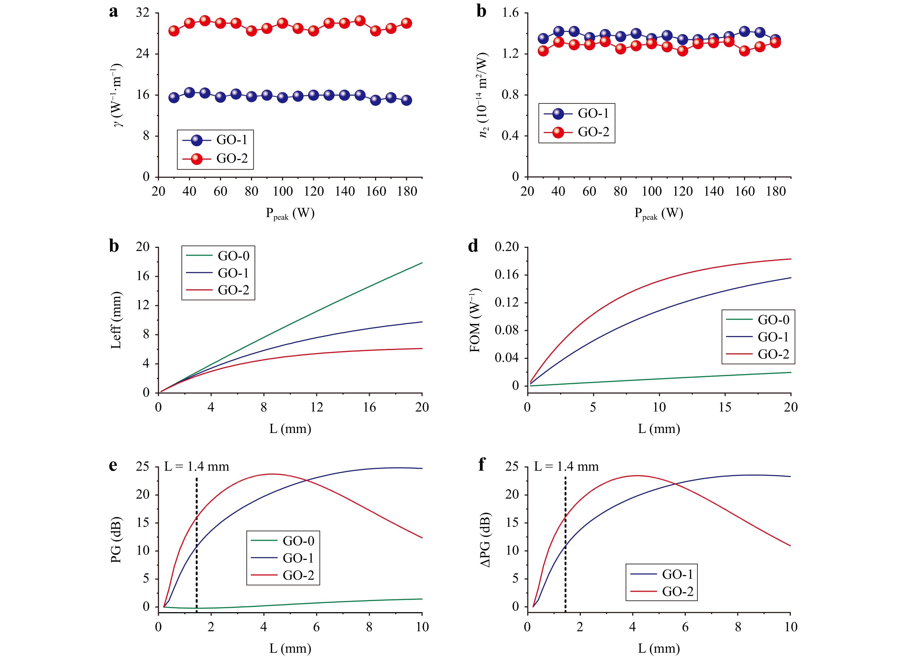
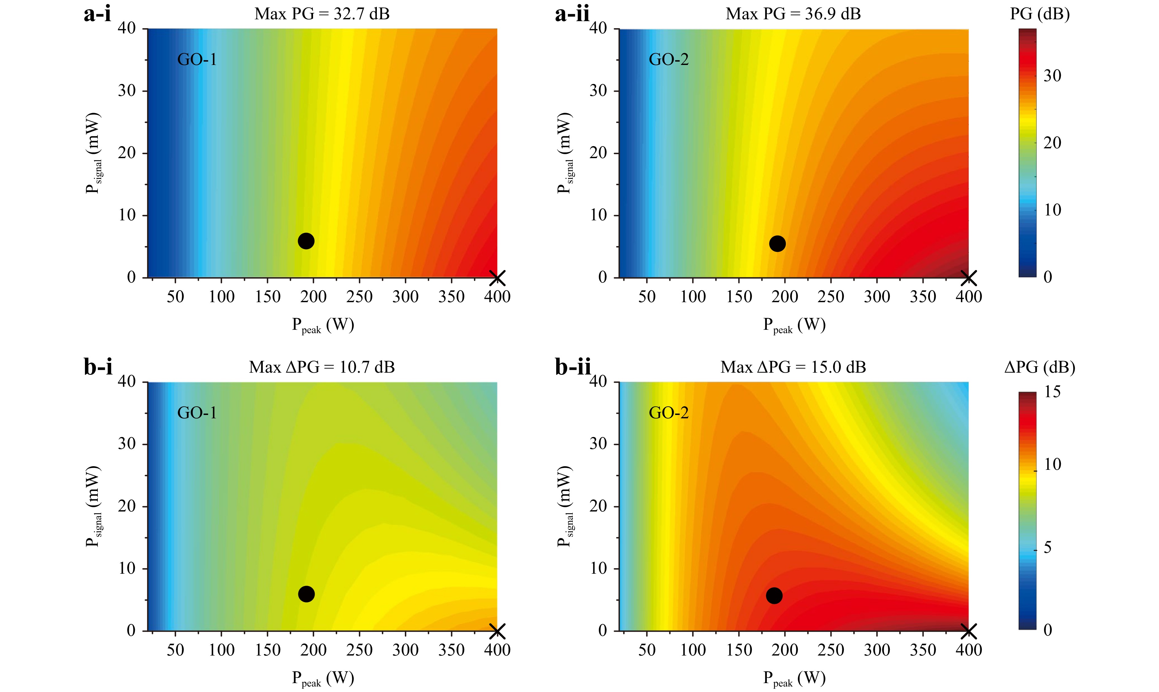
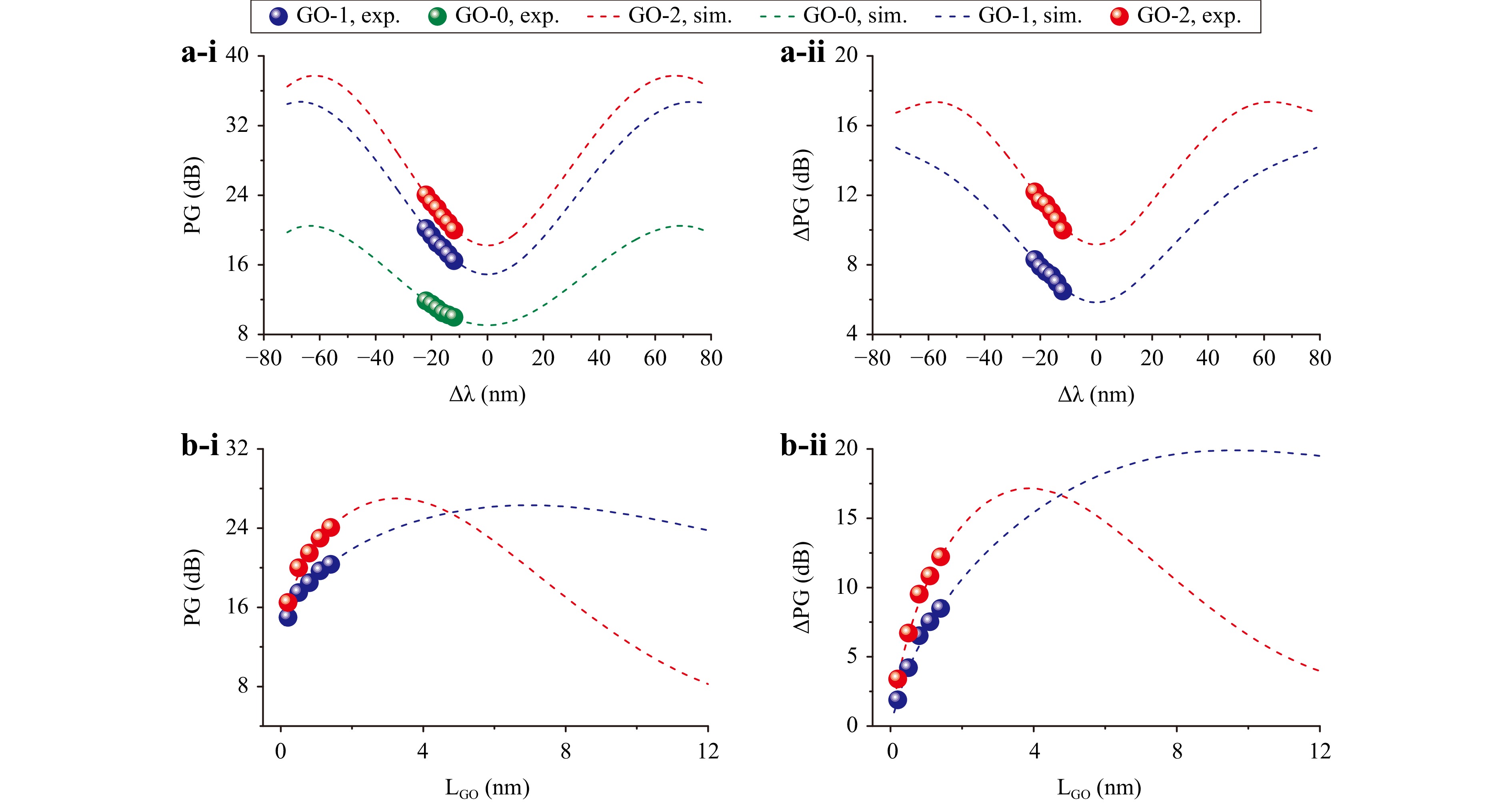
Optical parametric amplification (OPA) represents a powerful solution to achieve broadband amplification in wavelength ranges beyond the scope of conventional gain media, for generating high-power optical pulses, optical microcombs, entangled photon pairs and a wide range of other applications. Here, we demonstrate optical parametric amplifiers based on silicon nitride (Si3N4) waveguides integrated with two-dimensional (2D) layered graphene oxide (GO) films. We achieve precise control over the thickness, length, and position of the GO films using a transfer-free, layer-by-layer coating method combined with accurate window opening in the chip cladding using photolithography. Detailed OPA measurements with a pulsed pump for the fabricated devices with different GO film thicknesses and lengths show a maximum parametric gain of ~24.0 dB, representing a ~12.2 dB improvement relative to the device without GO. We perform a theoretical analysis of the device performance, achieving good agreement with experiment and showing that there is substantial room for further improvement. This work represents the first demonstration of integrating 2D materials on chips to enhance the OPA performance, providing a new way of achieving high performance photonic integrated OPA by incorporating 2D materials.
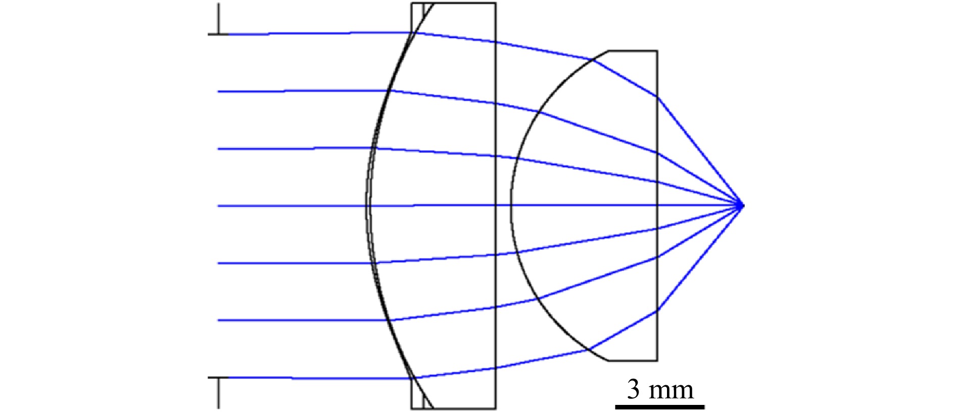
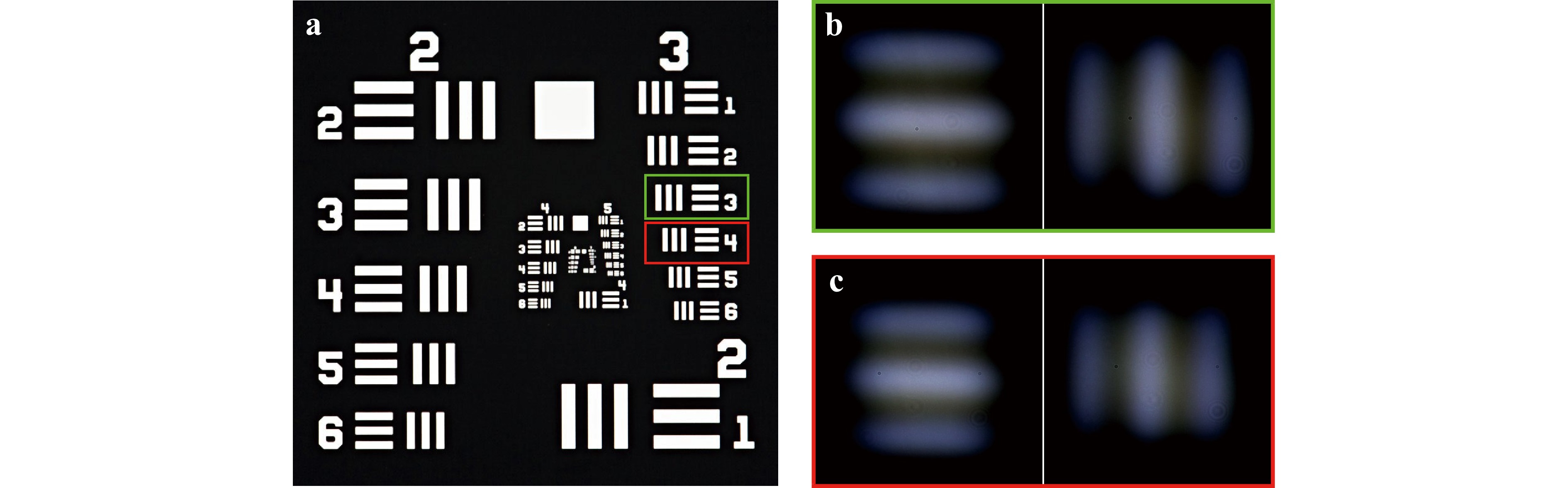
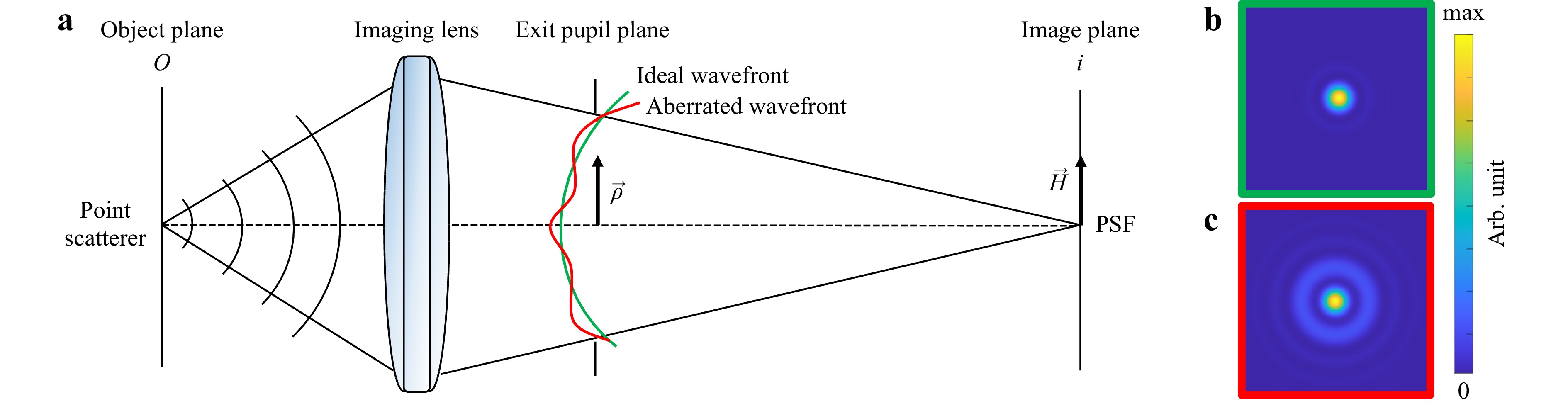
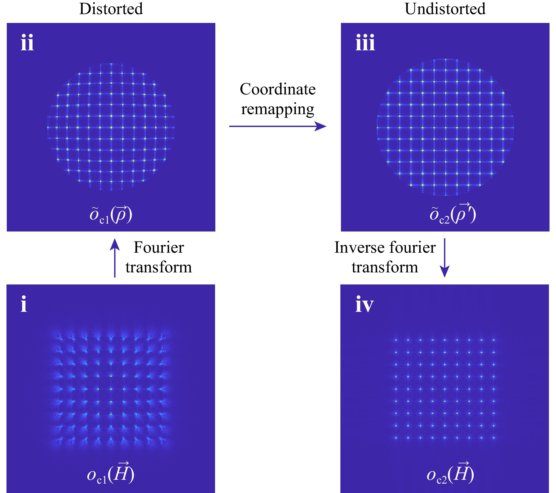
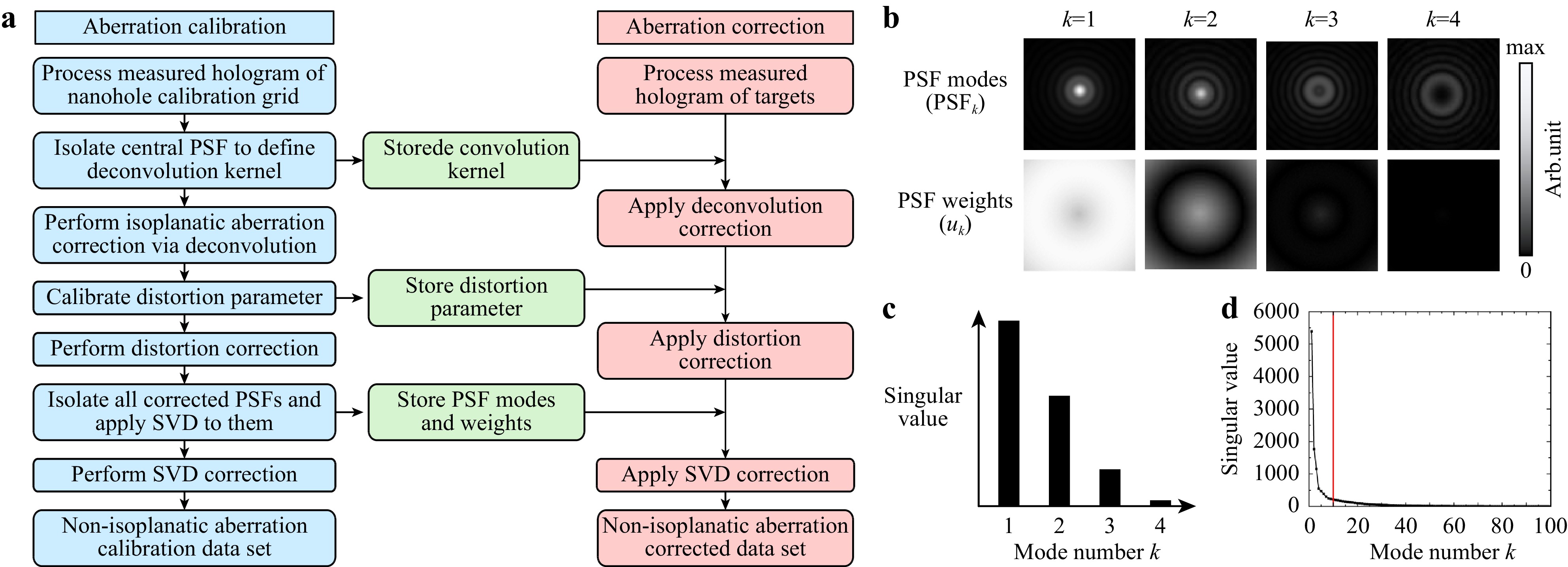
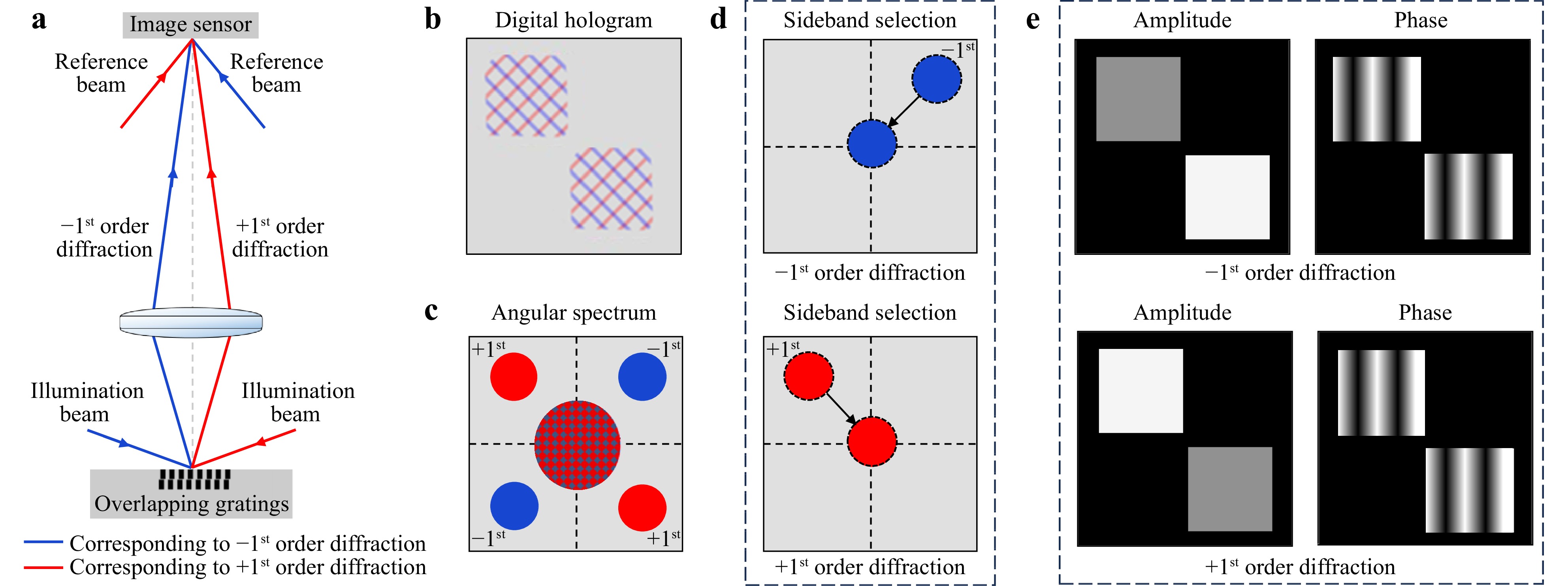
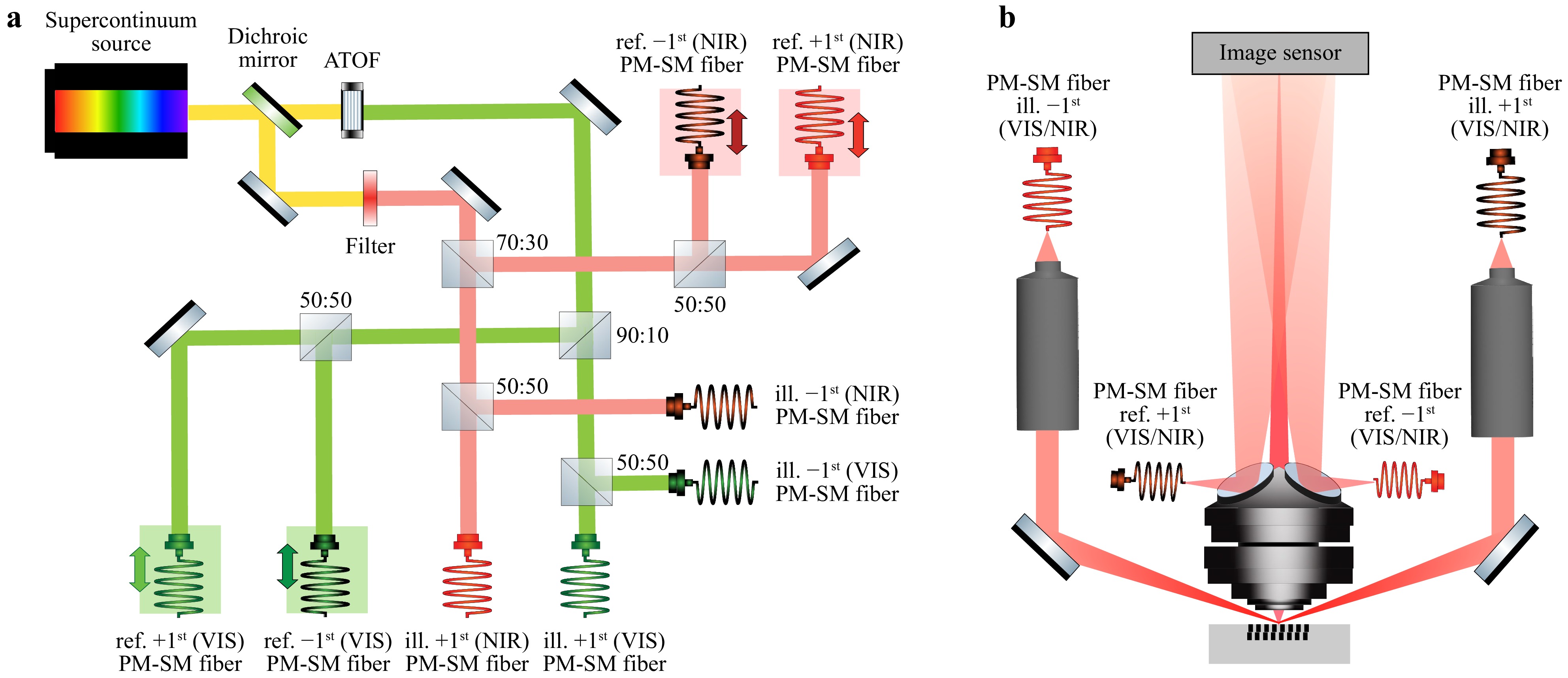
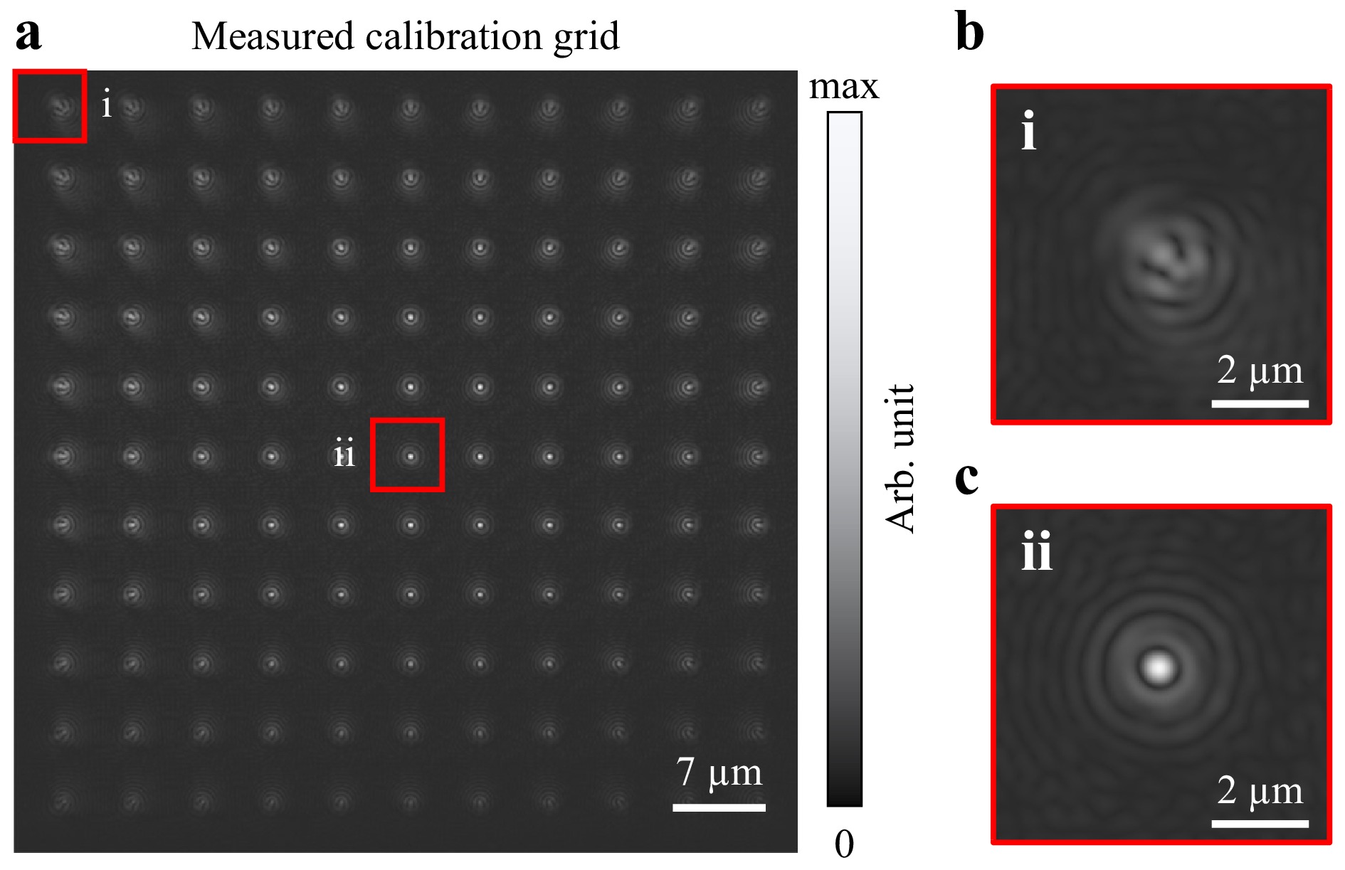
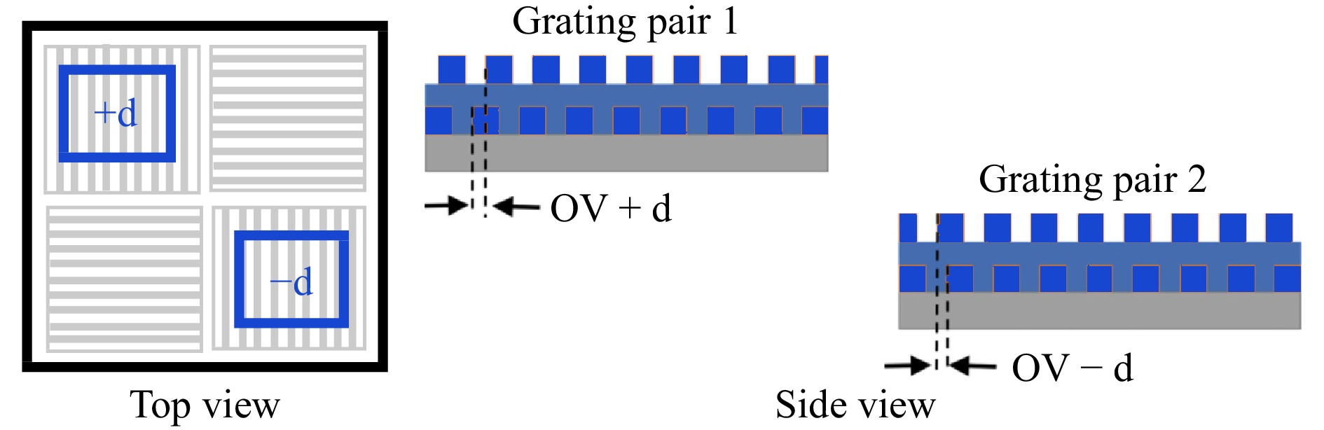
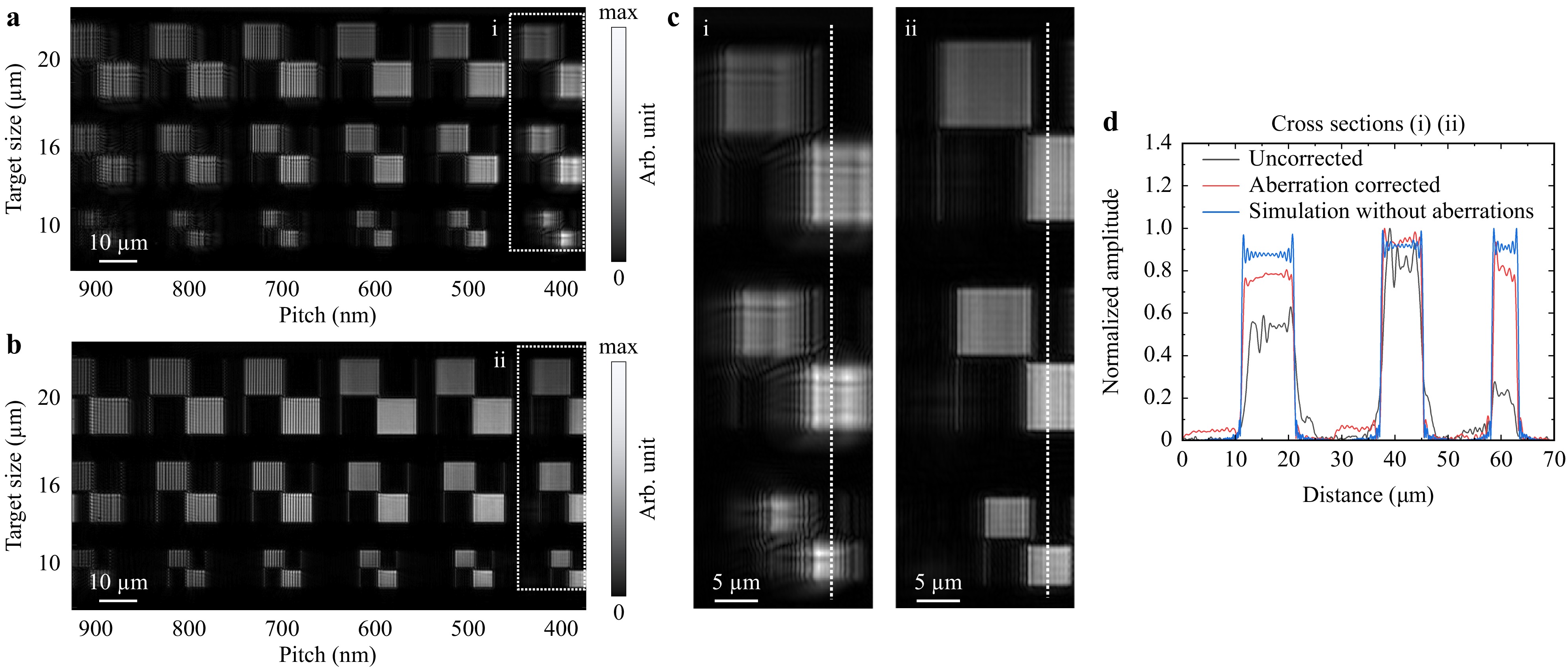
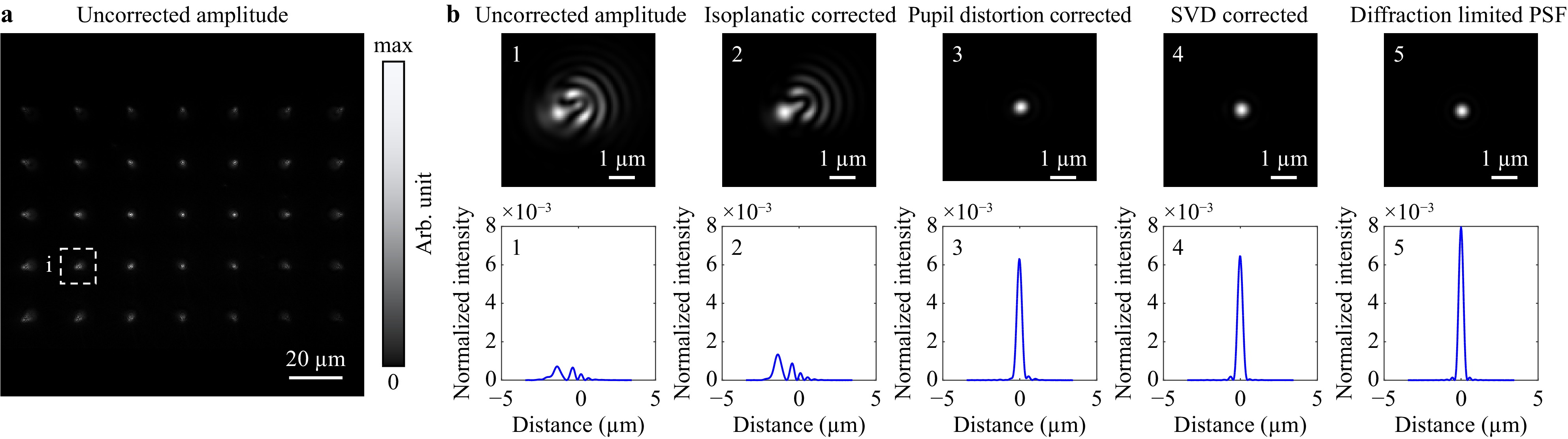
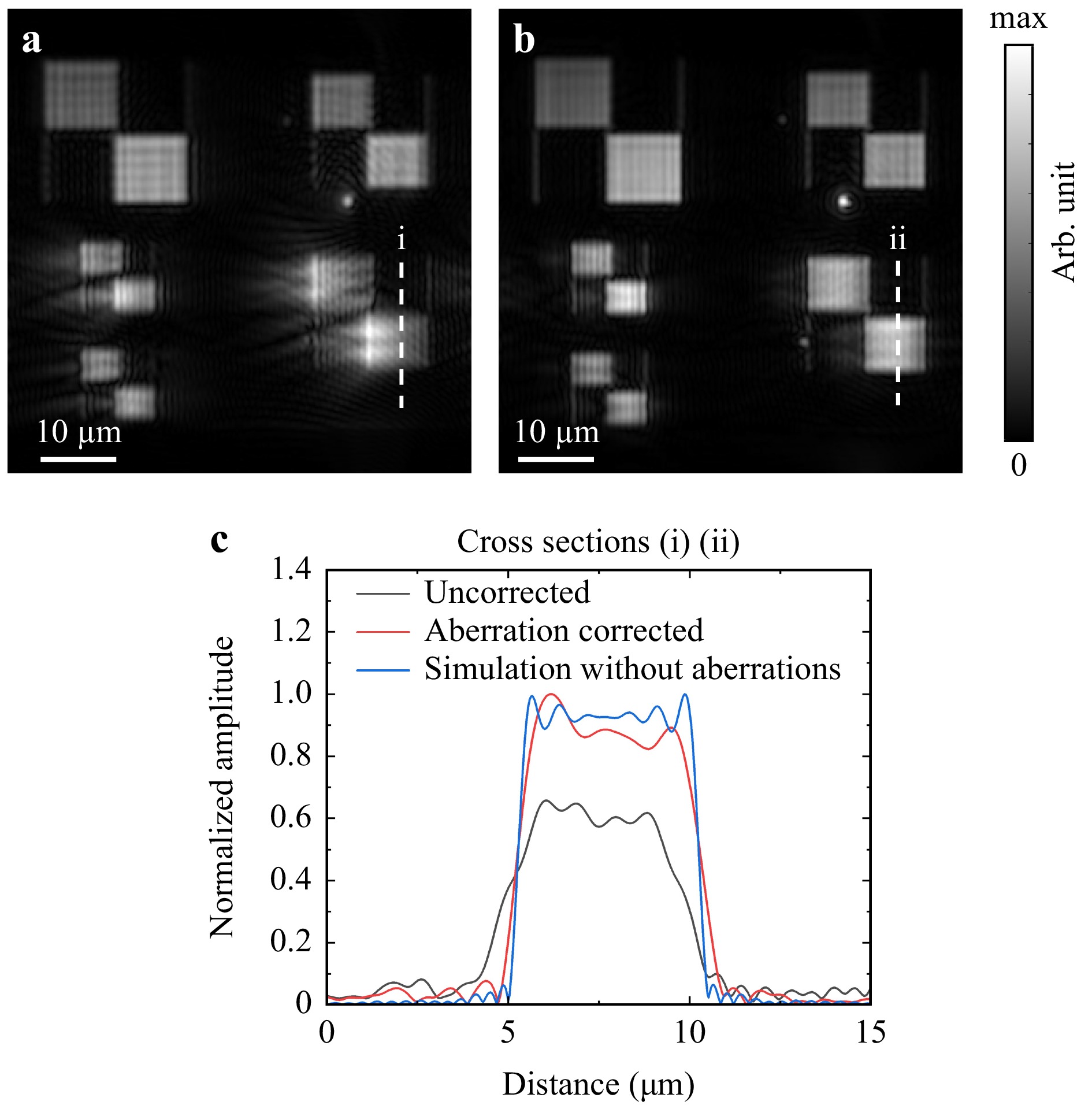
In the semiconductor industry, the demand for more precise and accurate overlay metrology tools has increased because of the continued shrinking of feature sizes in integrated circuits. To achieve the required sub-nanometre precision, the current technology for overlay metrology has become complex and is reaching its limits. Herein, we present a dark-field digital holographic microscope using a simple two-element imaging lens with a high numerical aperture capable of imaging from the visible to near-infrared regions. This combination of high resolution and wavelength coverage was achieved by combining a simple imaging lens with a fast and accurate correction of non-isoplanatic aberrations. We present experimental results for overlay targets that demonstrate the capability of our computational aberration correction in the visible and near-infrared wavelength regimes. This wide-ranged-wavelength imaging system can advance semiconductor metrology.
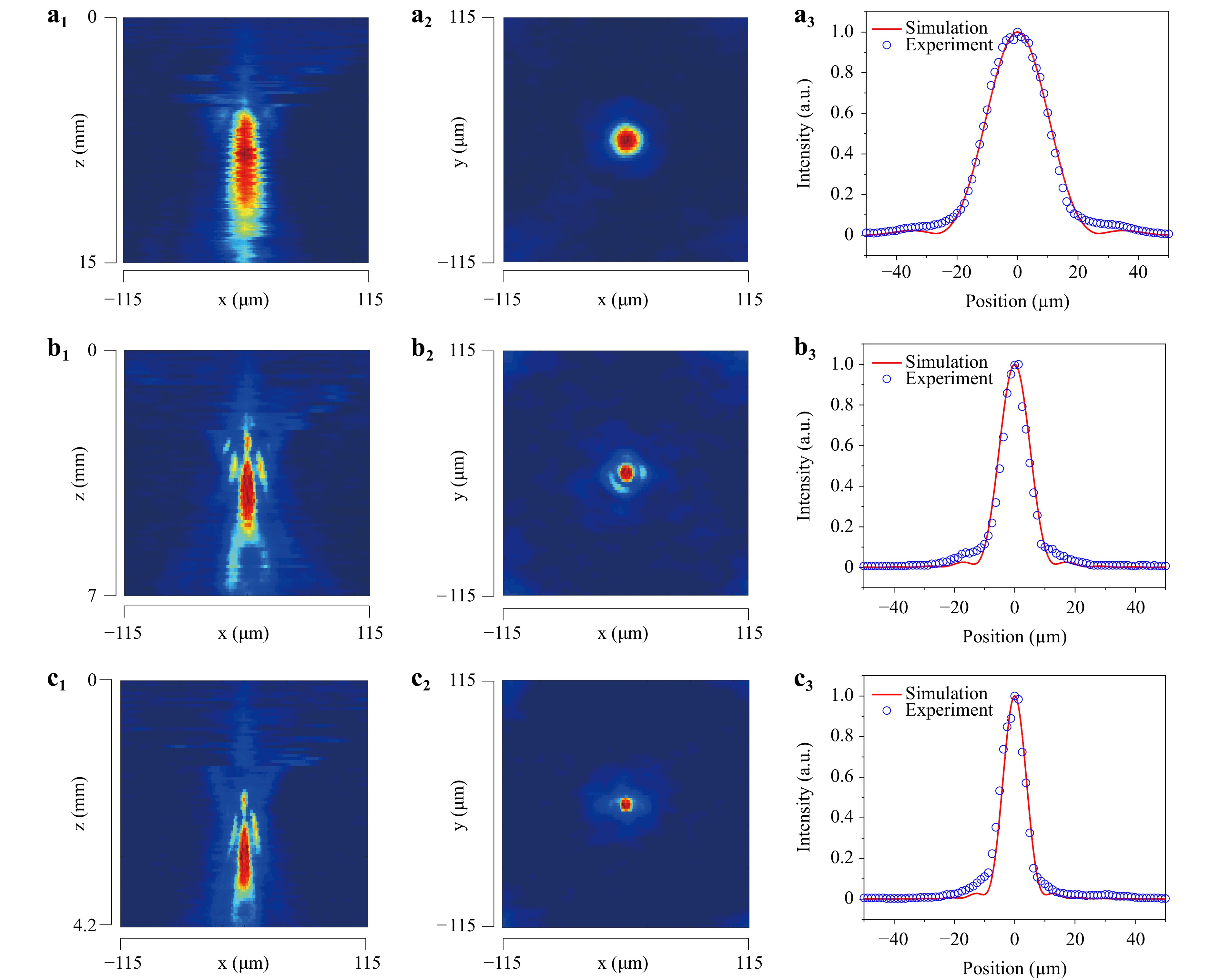
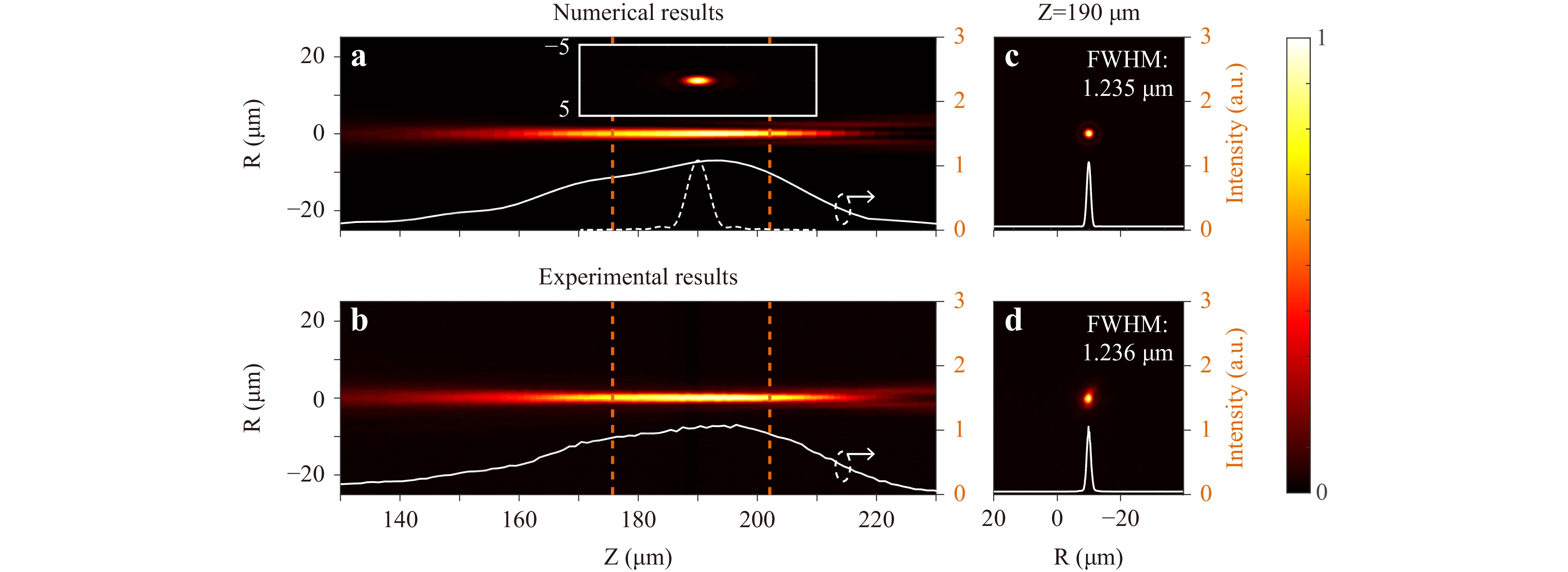
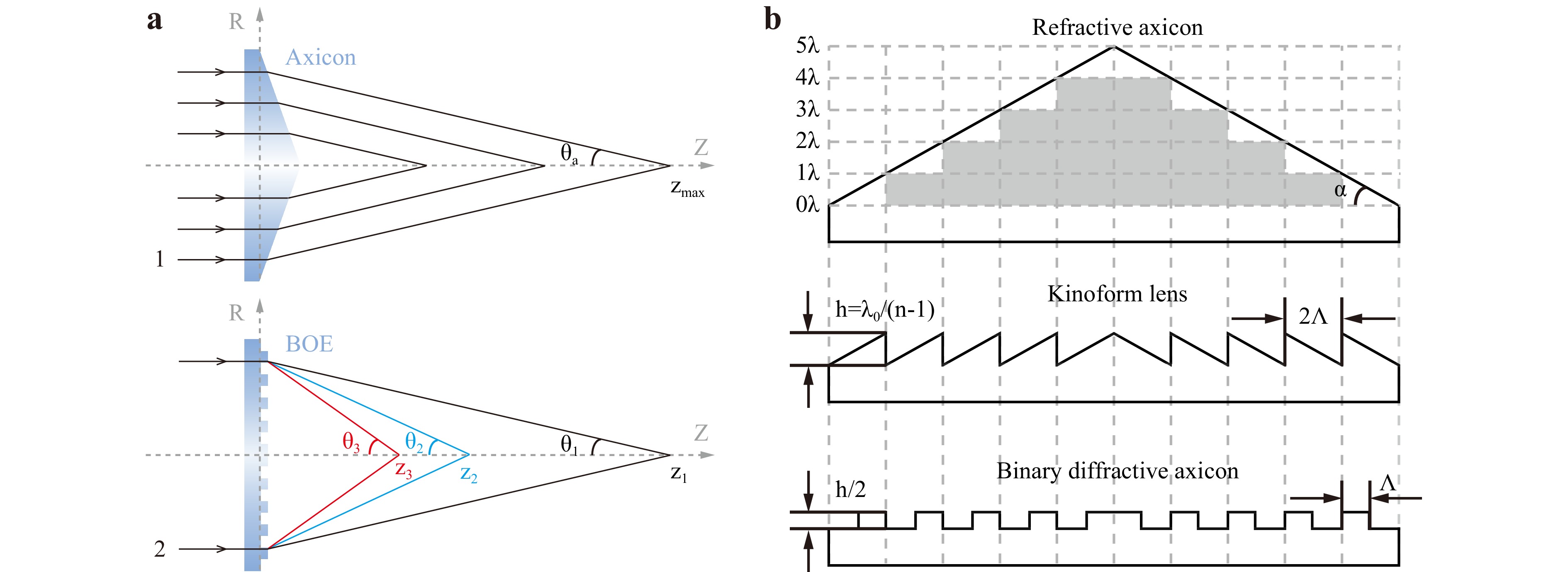
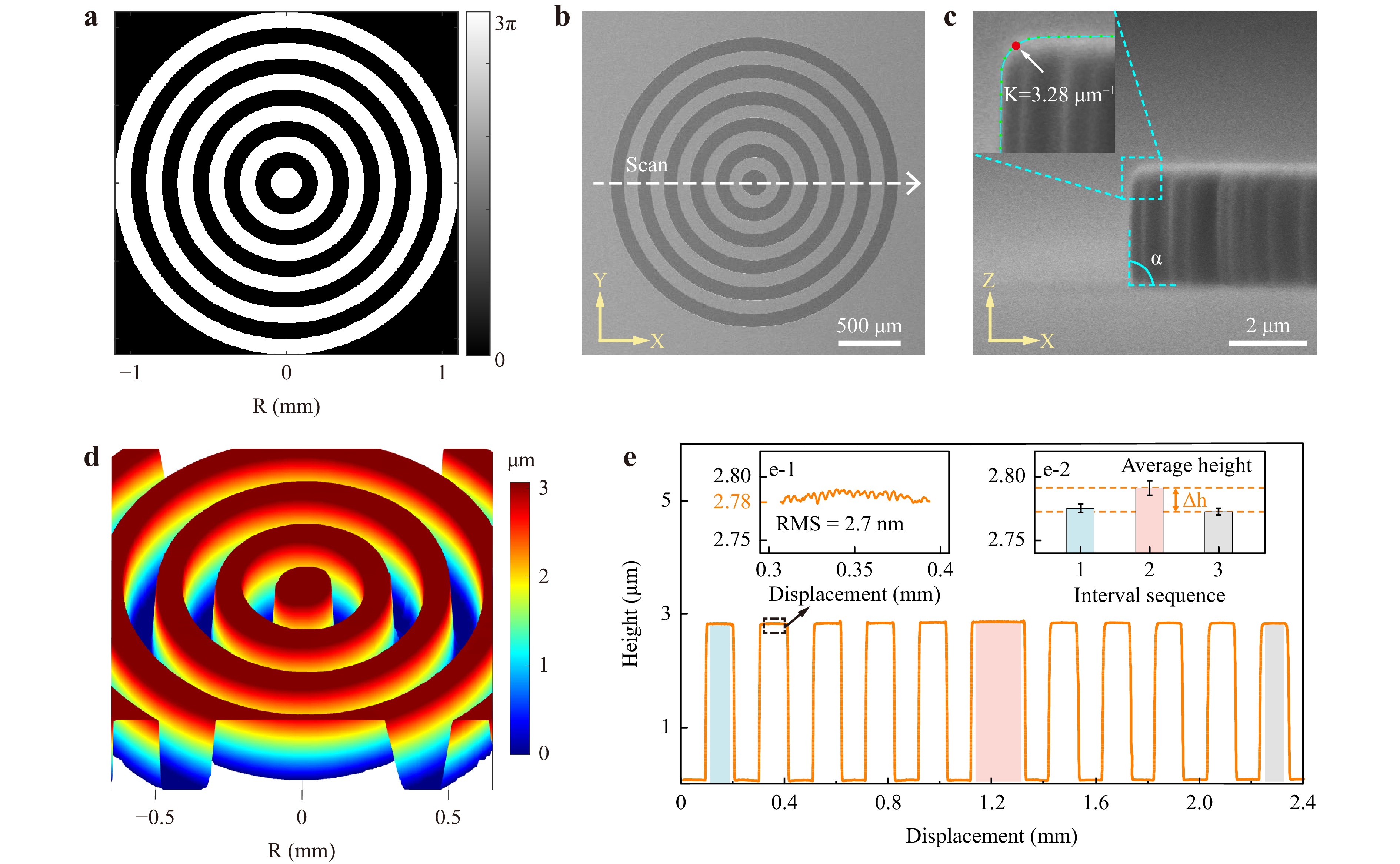
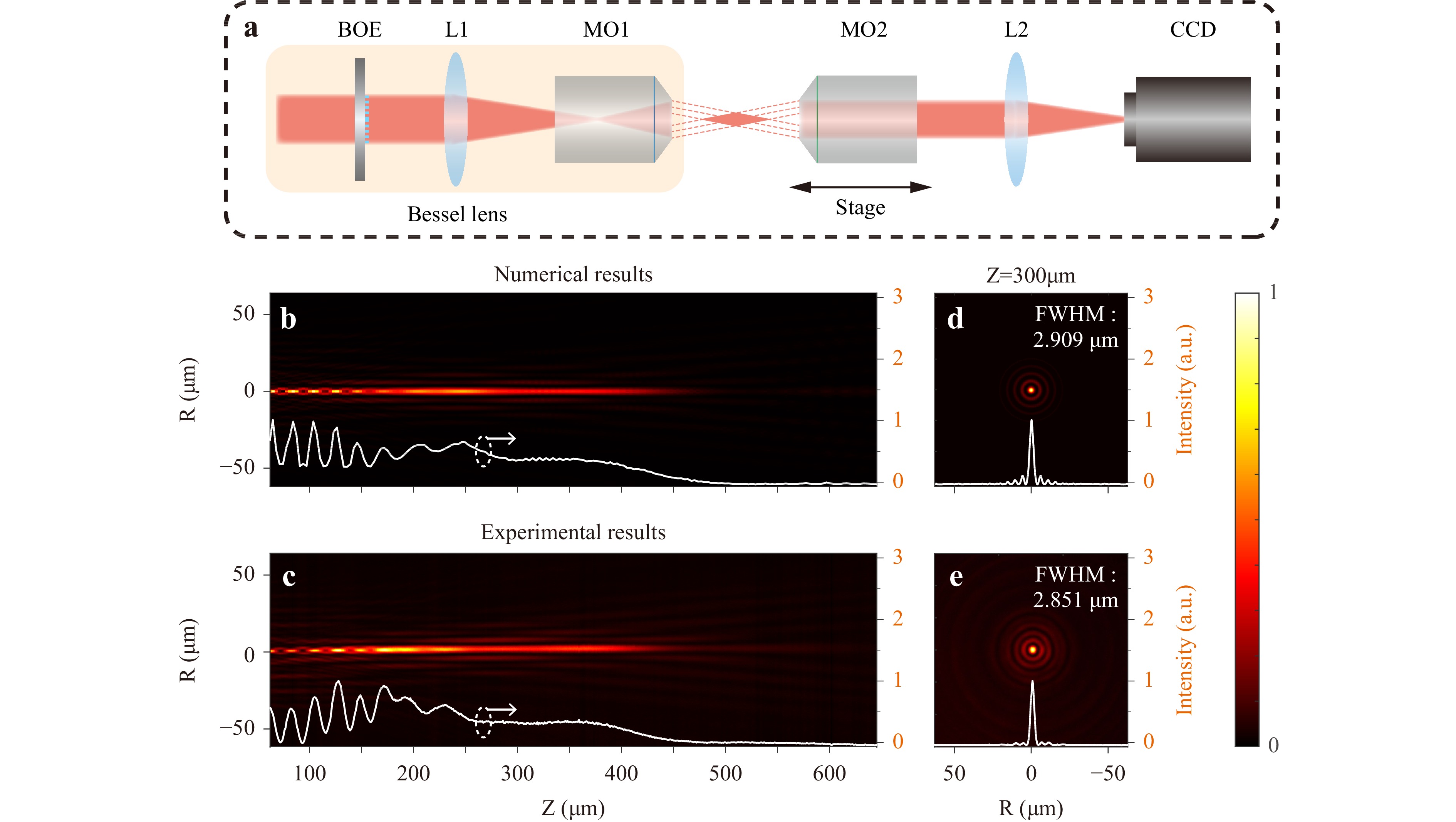
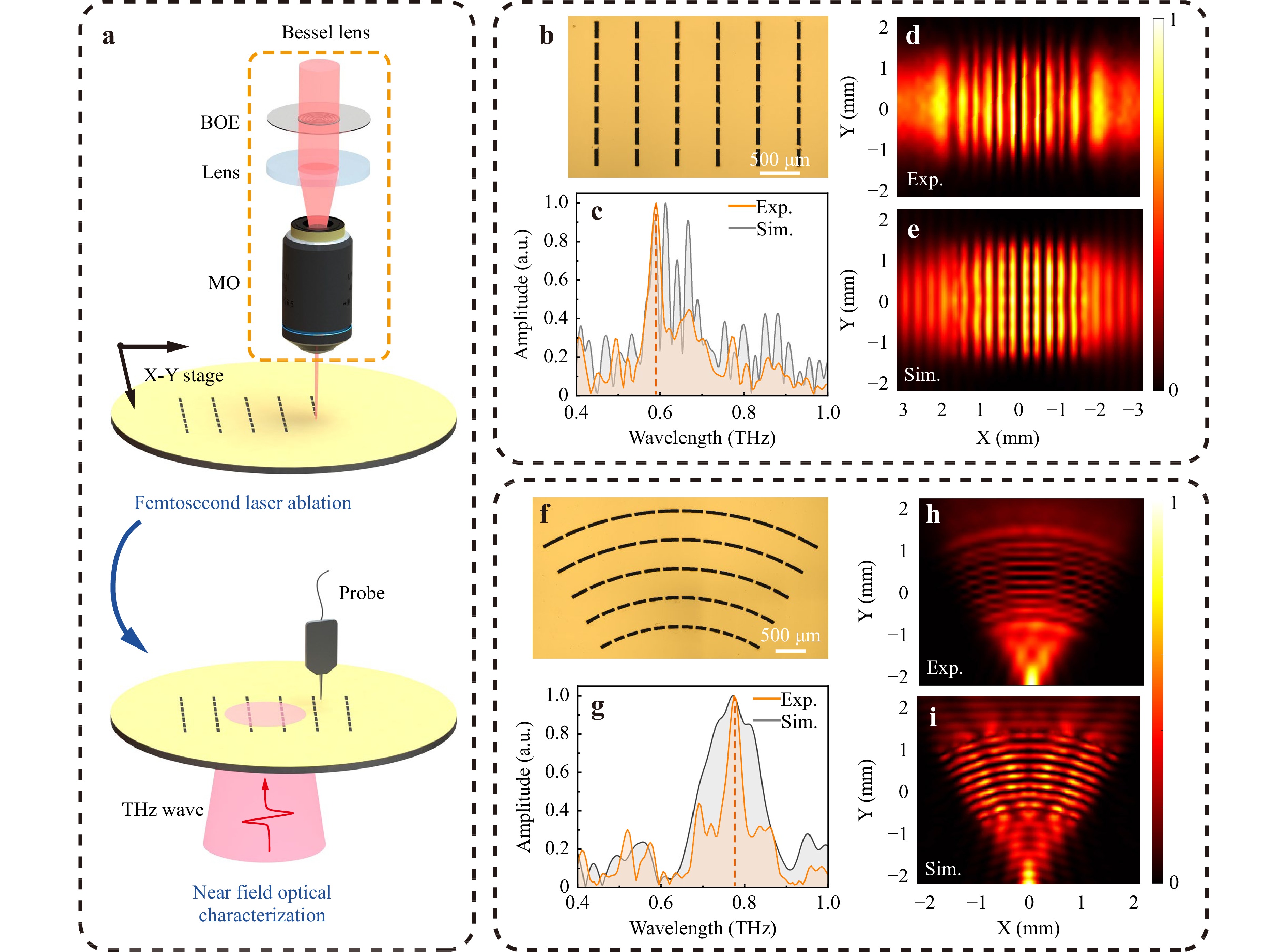
Bessel beams have multiple applications owing to their propagation-invariant properties, including particle trapping, optical coherence tomography, and material processing. However, traditional Bessel-beam shaping techniques require bulky components, which limits the development of miniaturized optical systems for integration with other devices. Here, we report a novel femtosecond laser direct writing strategy for fabricating mesoscale (from submicrometer to subcentimeter) binary optical elements with microscale resolution. This strategy utilizes femtosecond beams with a long focal depth to increase throughput while reducing the constraints on critical sample positioning. As a demonstration, we manufactured and characterized a 2.2 mm diameter binary axicon. The experimentally measured quasi-Bessel beam intensity distribution and the numerical results were remarkably consistent, demonstrating a suitable tradeoff between the overall size, efficiency, and structural fidelity. Furthermore, a compact Bessel lens containing binary axicons was constructed and successfully used for femtosecond laser mask-less ablation of periodic grating-type surface plasmon polariton excitation units. The demonstrated approach shows significant potential for fabricating customizable integrated optical components.
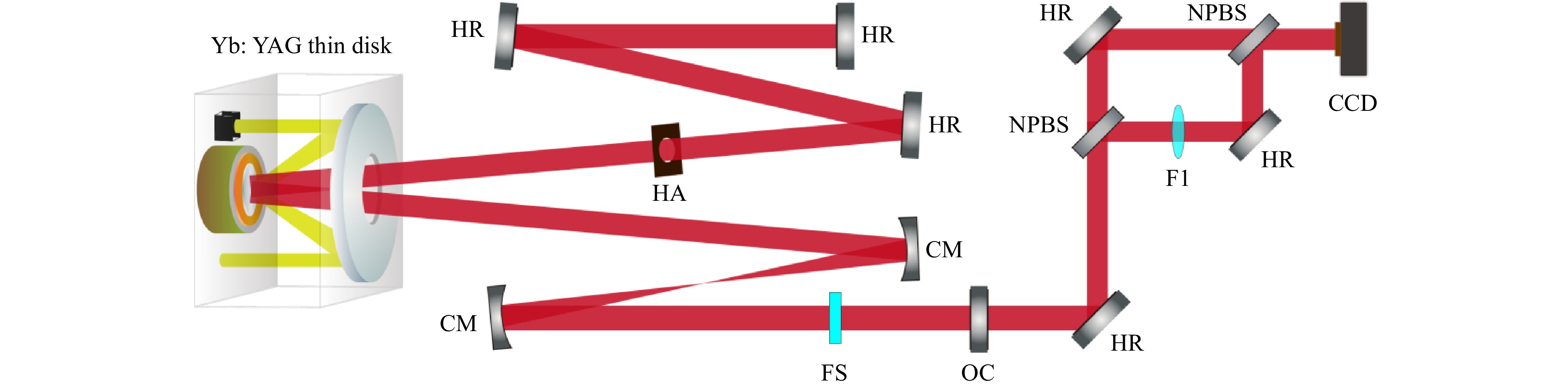
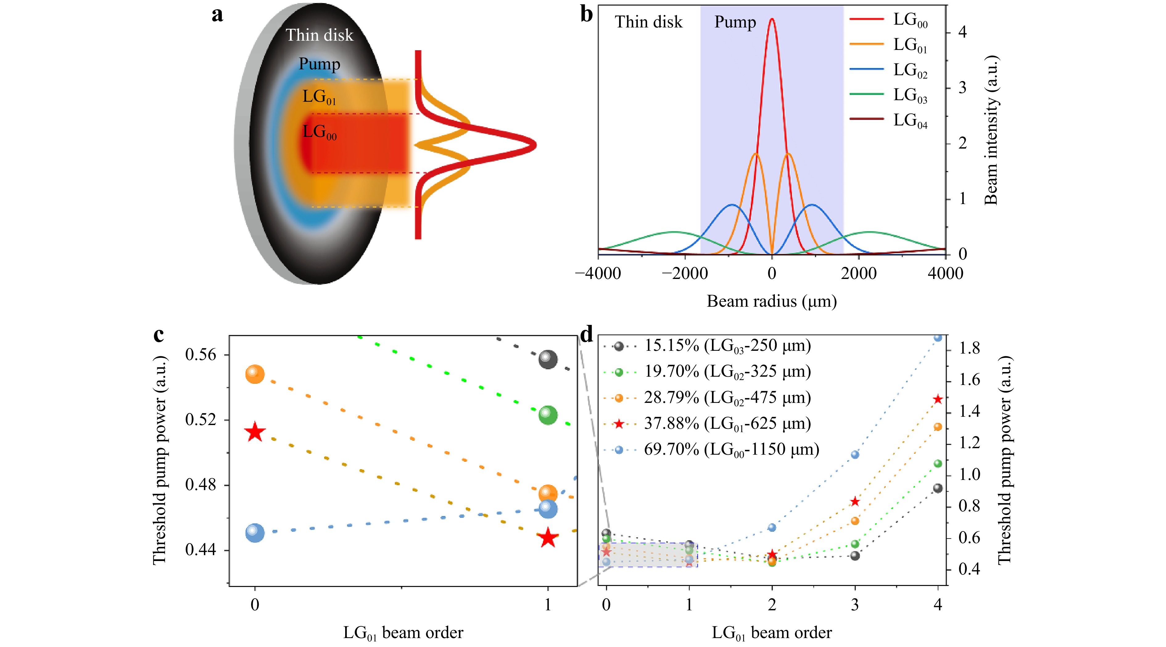
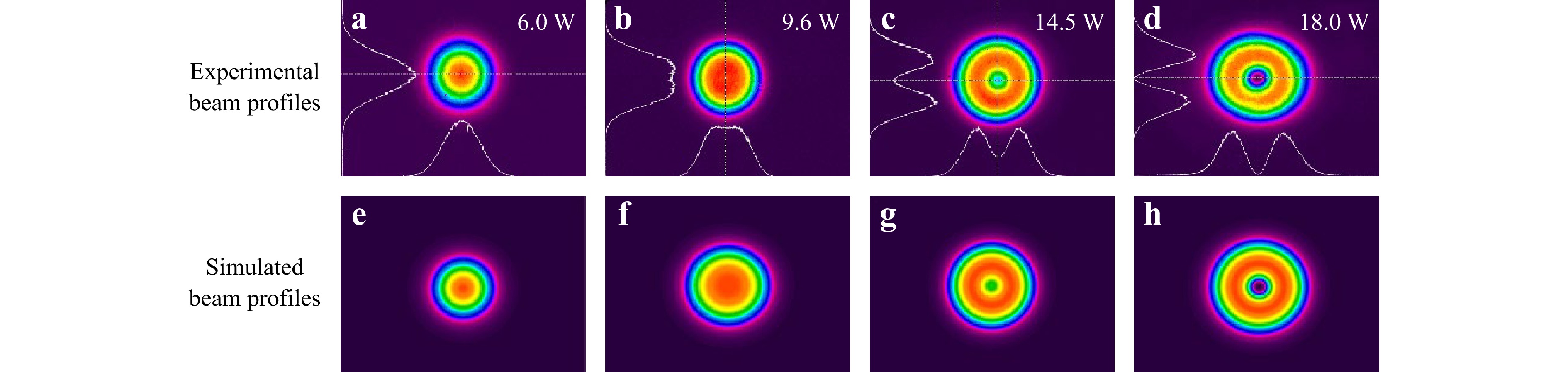
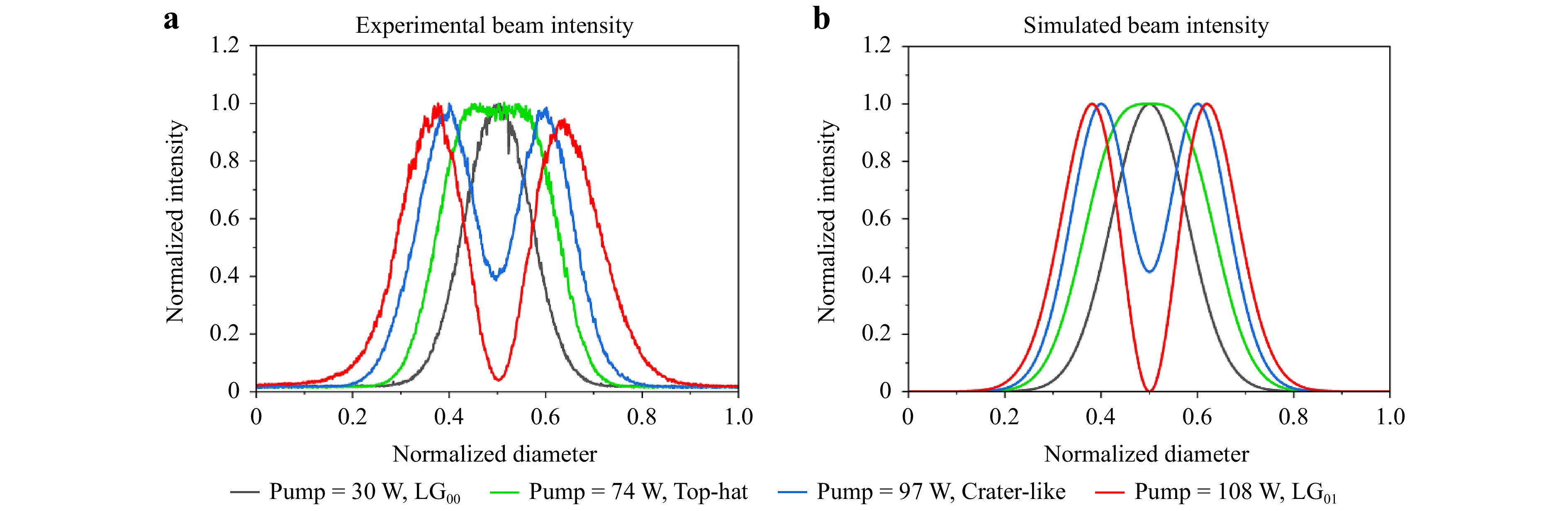
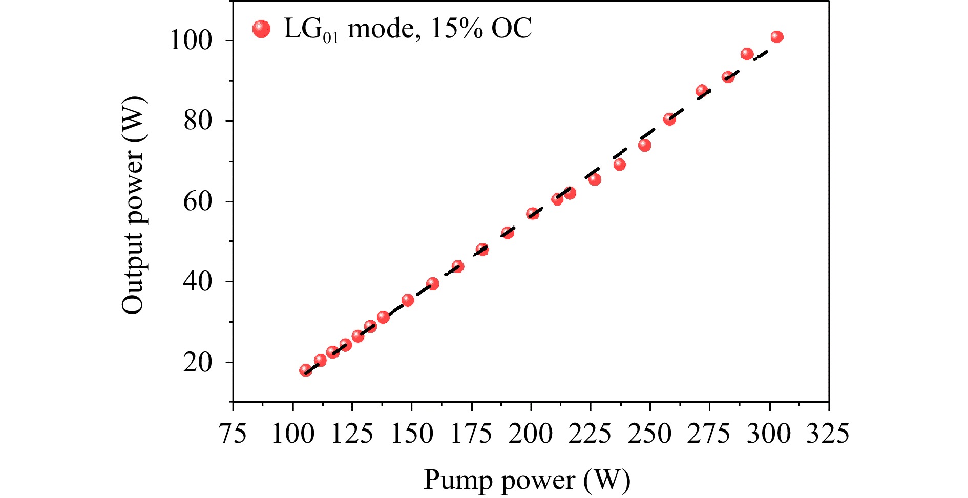
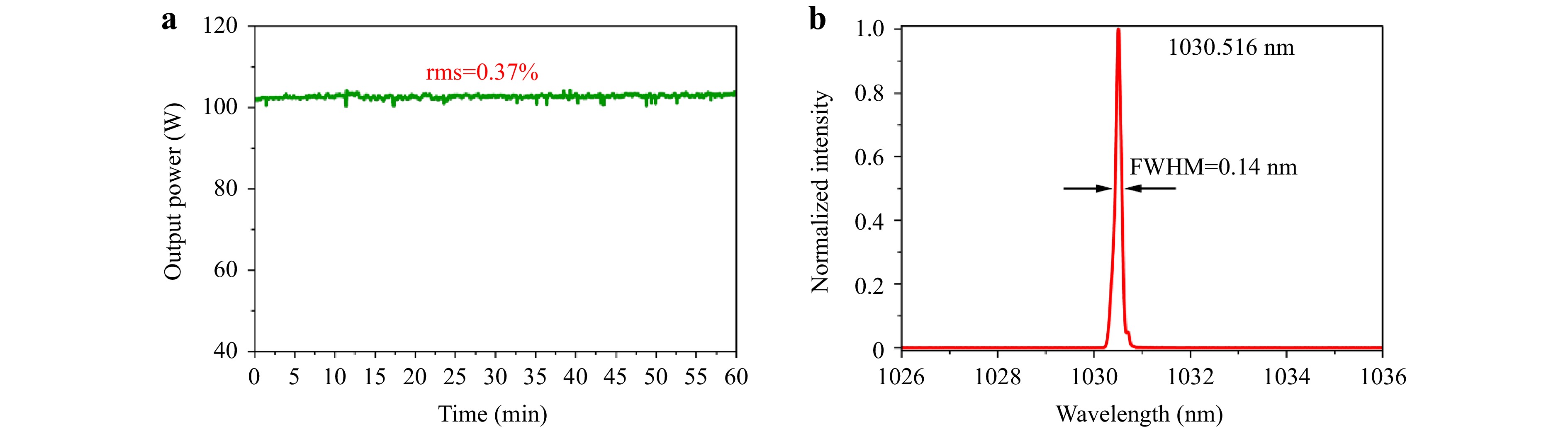
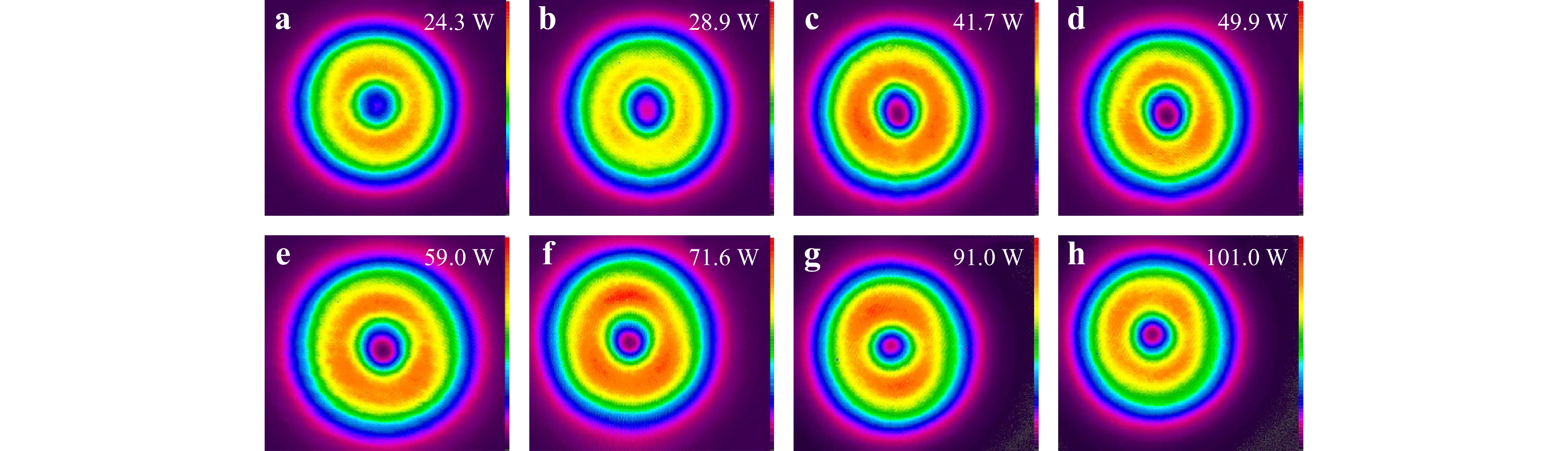
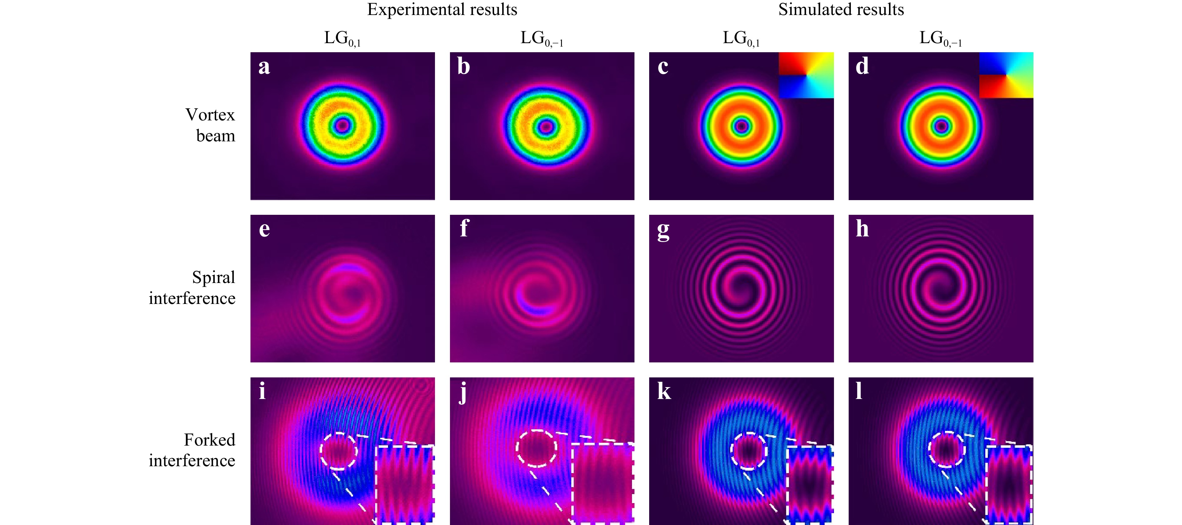
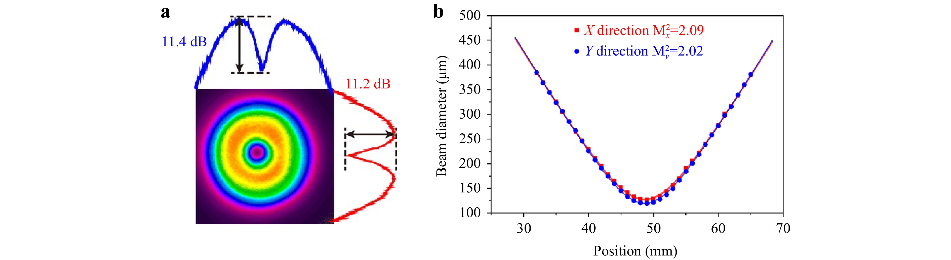
Optical vortices carrying orbital angular momentum and spiral wavefront phases have garnered increasing research interest owing to their numerous applications. Here, we present a simple yet effective approach to generate powerful optical vortices directly from a thin-disk laser oscillator. The demonstrated source delivered Laguerre–Gaussian beams with an output power of up to 101 W. To the best of our knowledge, this is the highest output power of all optical vortex laser oscillators. The high-power vortex output will have significant implications for laser ablation and micromachining at high throughput and for large-area applications. Additionally, it serves as a new platform for the further development of more complex high-power optical-vortex beams.
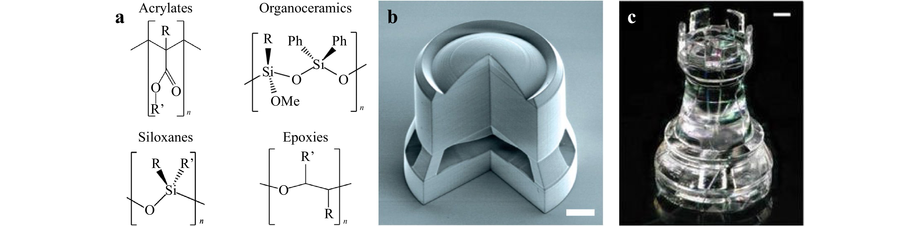
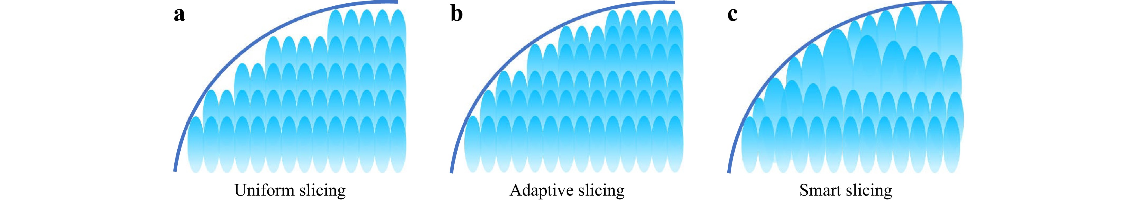
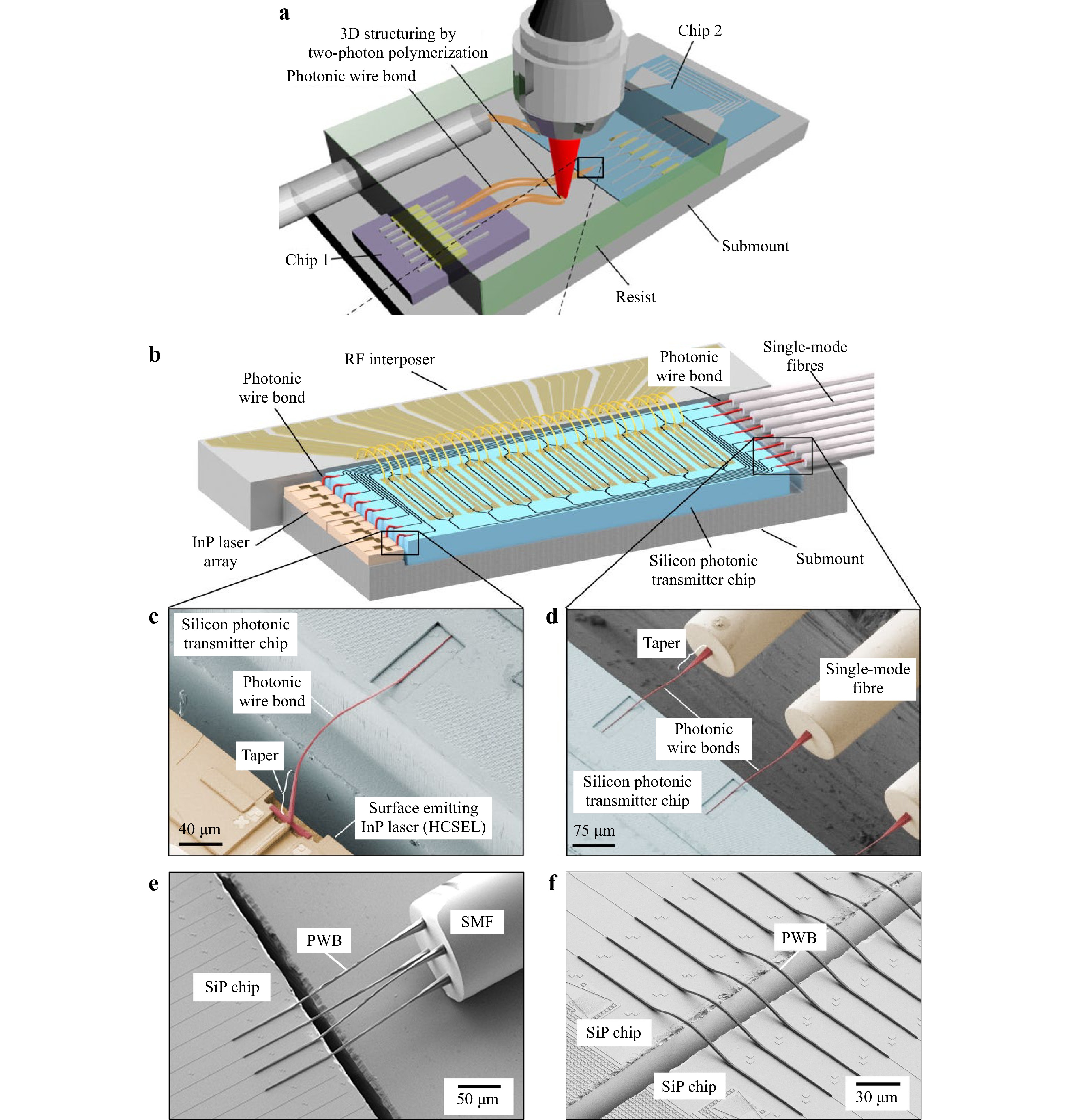
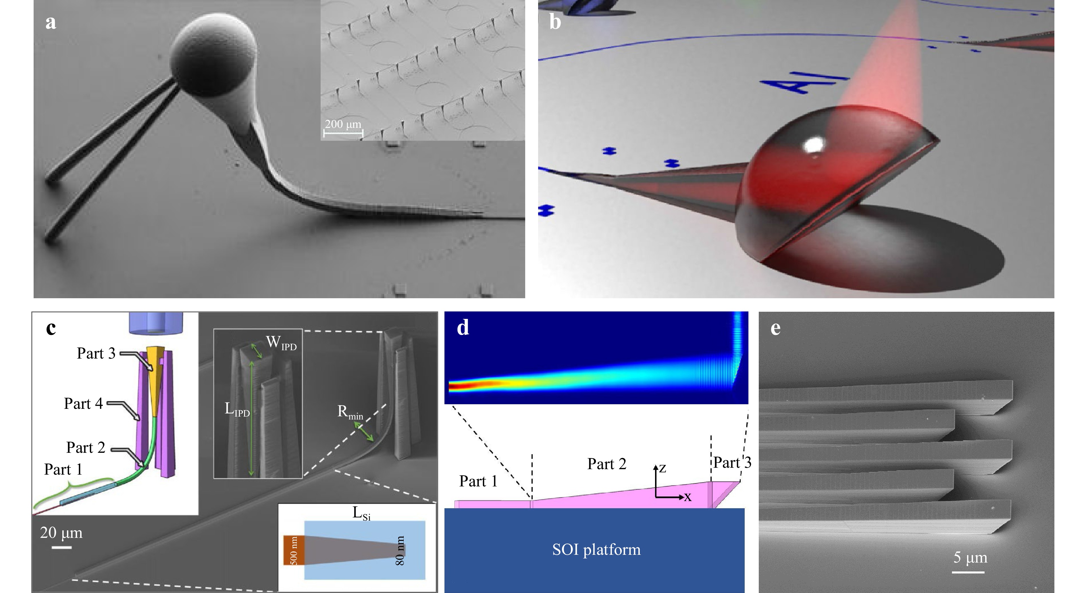
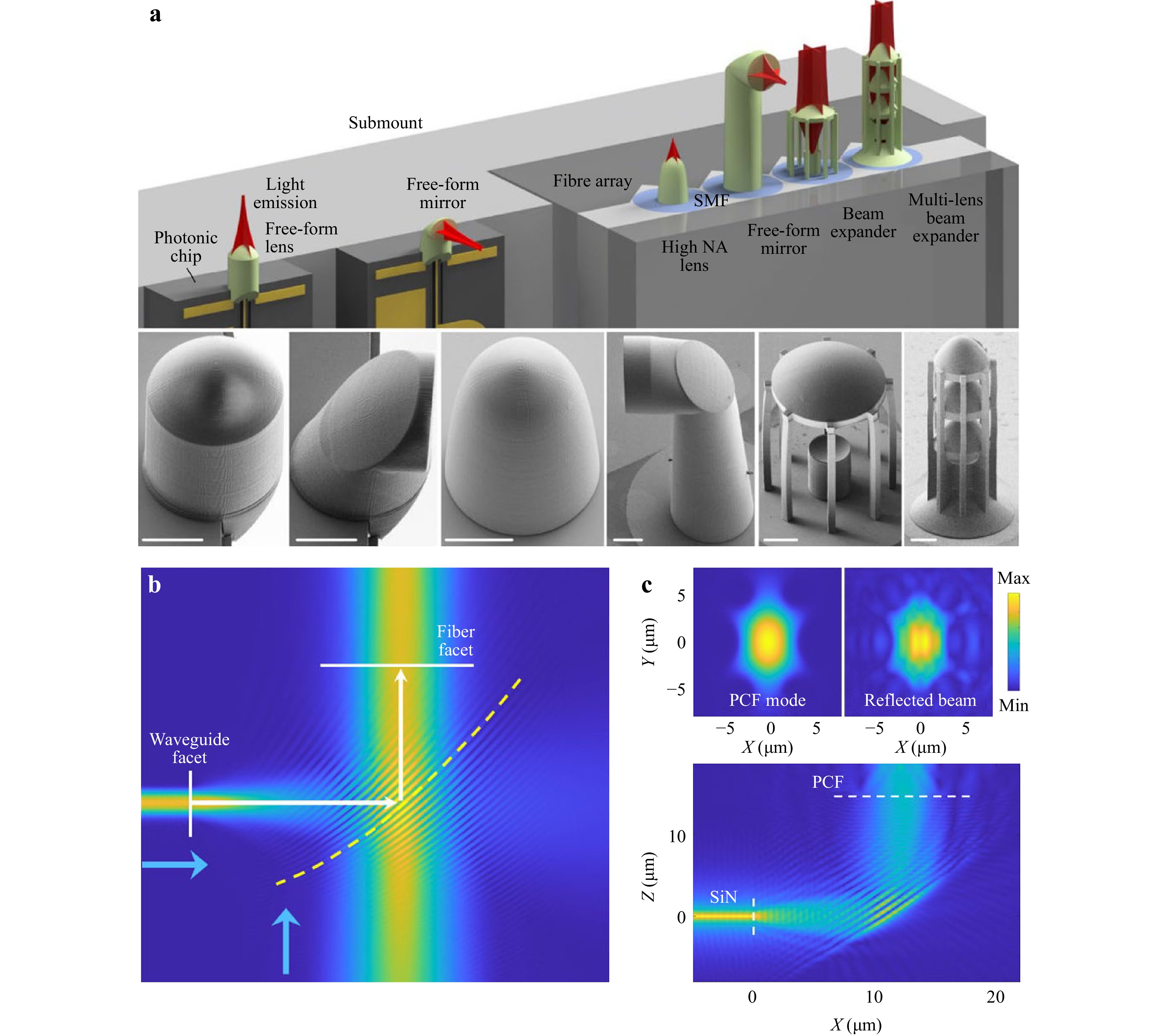
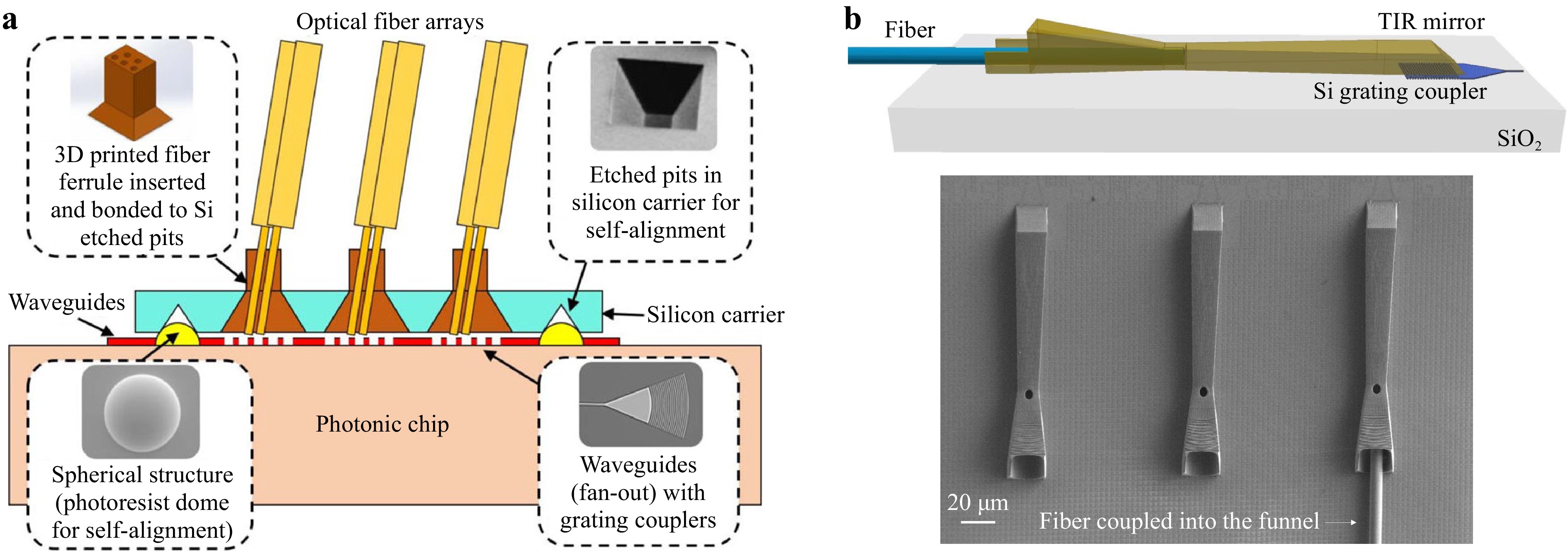
Photonic integrated circuits (PICs) have long been considered as disruptive platforms that revolutionize optics. Building on the mature industrial foundry infrastructure for electronic integrated circuit fabrication, the manufacturing of PICs has made remarkable progress. However, the packaging of PICs has often become a major barrier impeding their scalable deployment owing to their tight optical alignment tolerance, and hence, the requirement for specialty packaging instruments. Two-photon lithography (TPL), a laser direct-write three-dimensional (3-D) patterning technique with deep subwavelength resolution, has emerged as a promising solution for integrated photonics packaging. This study provides an overview of the technology, emphasizing the latest advances in TPL-enabled packaging schemes and their prospects for adoption in the mainstream photonic industry.
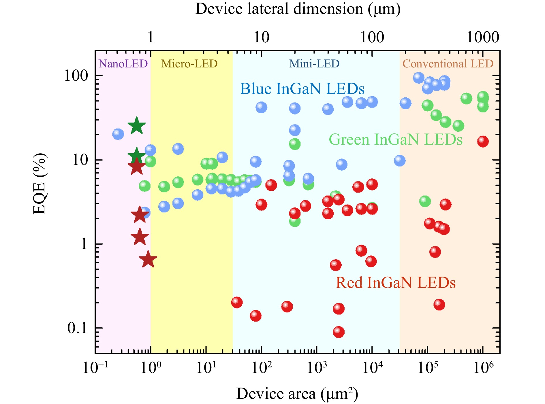
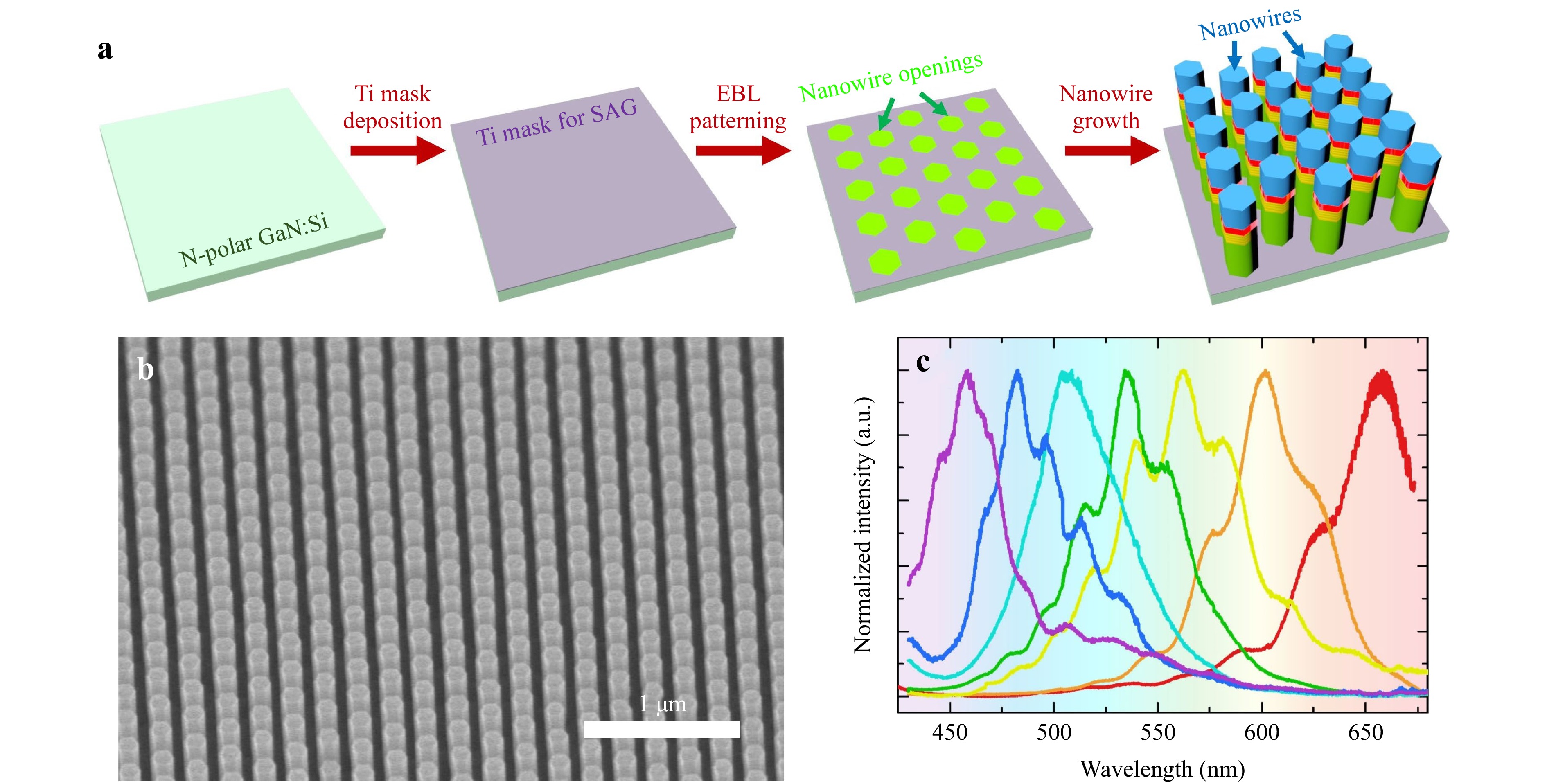
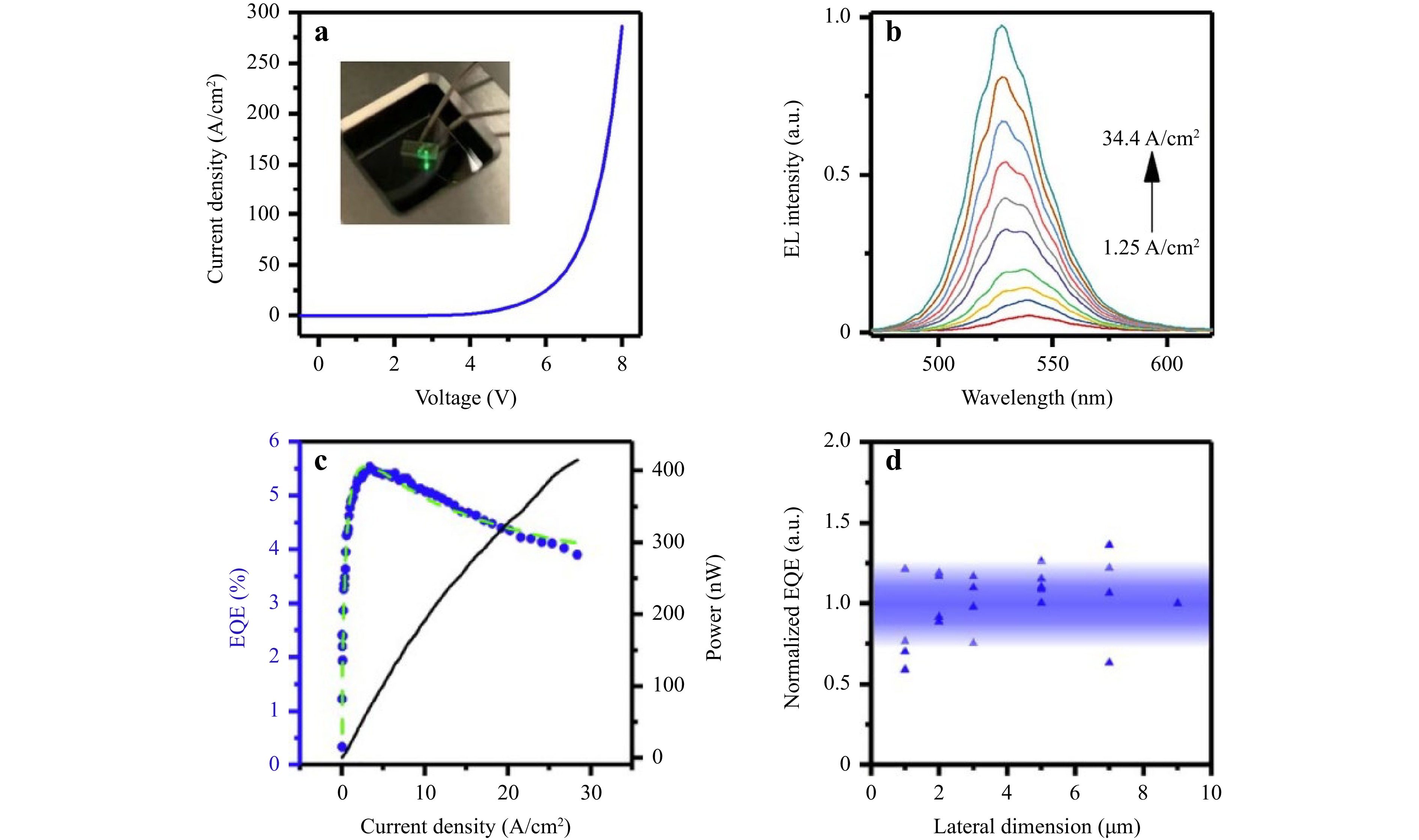
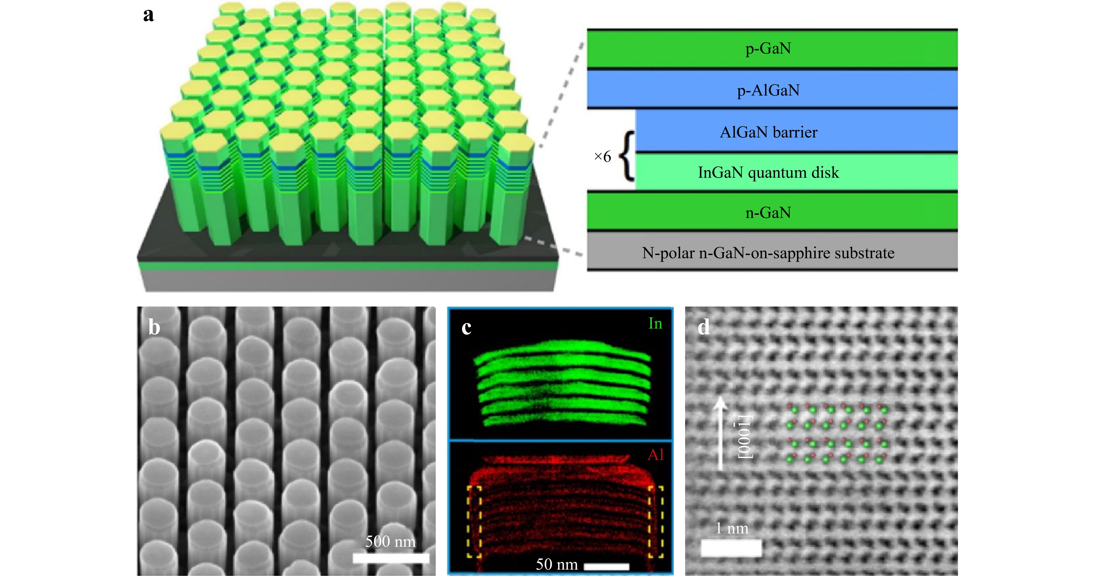
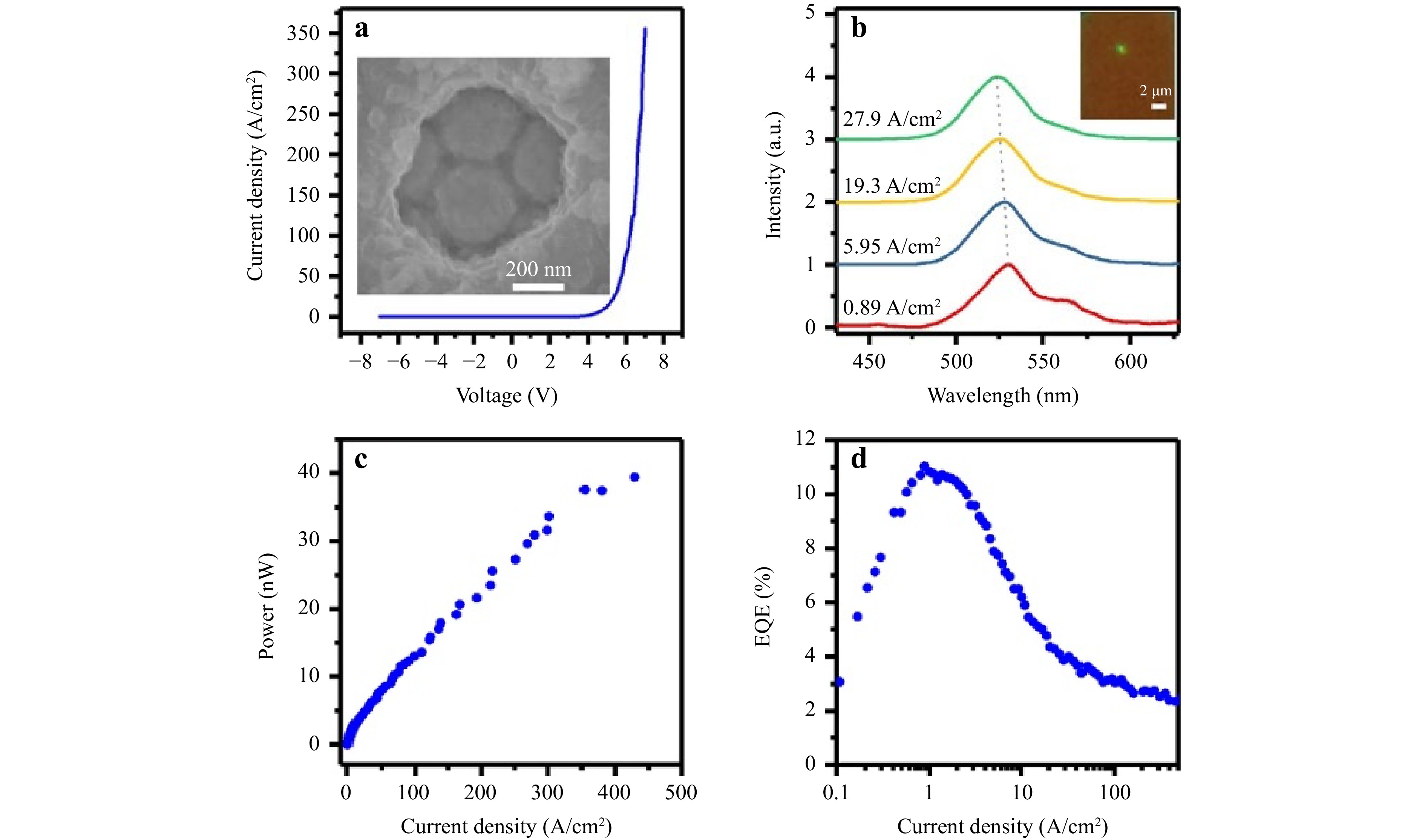
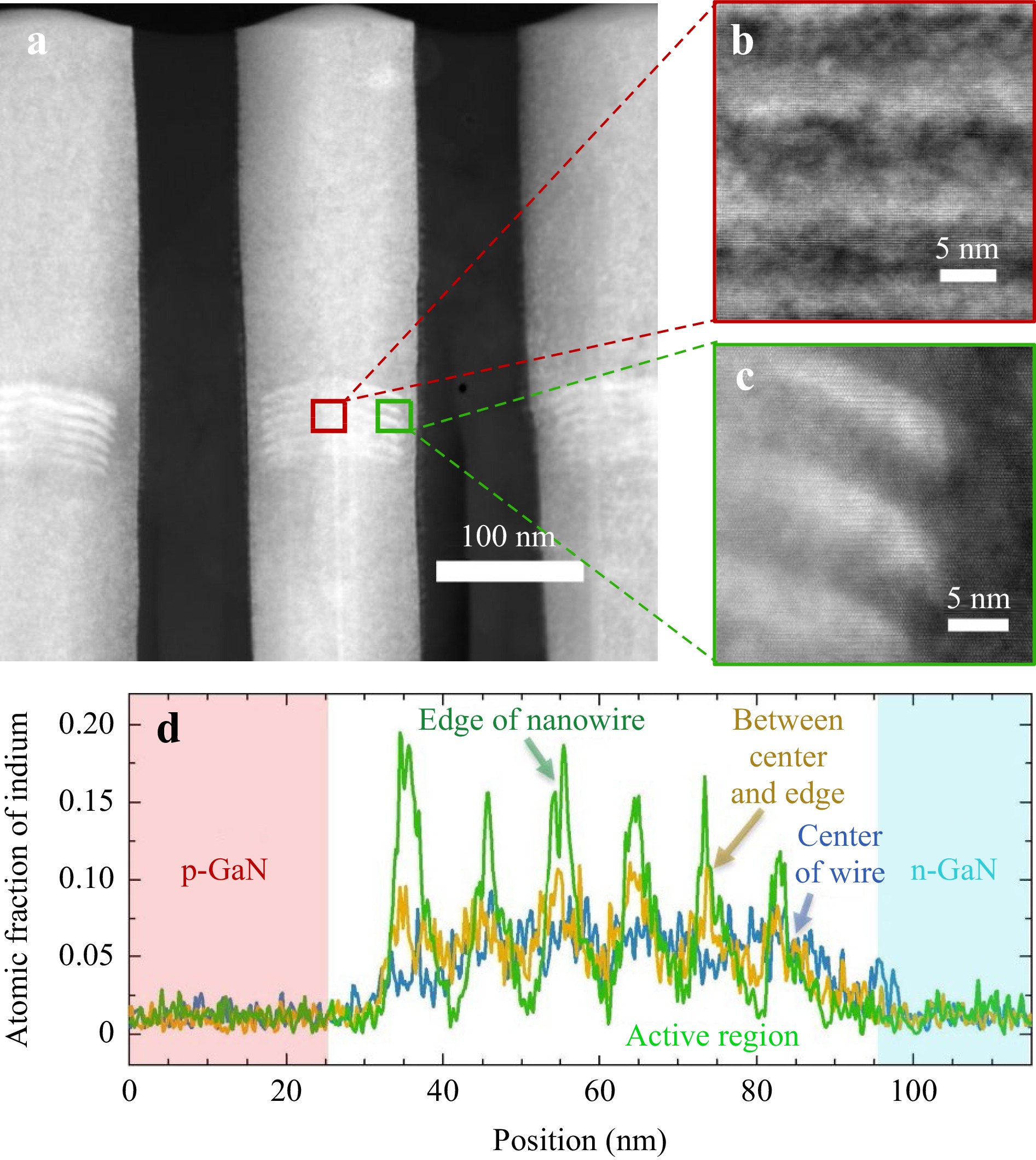
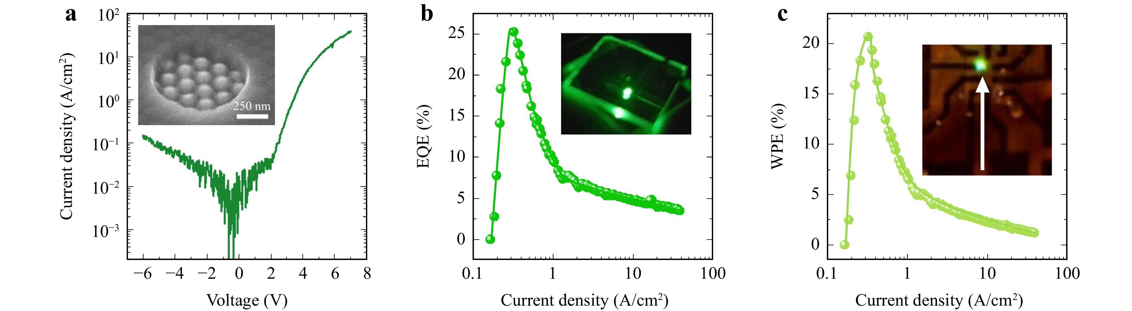
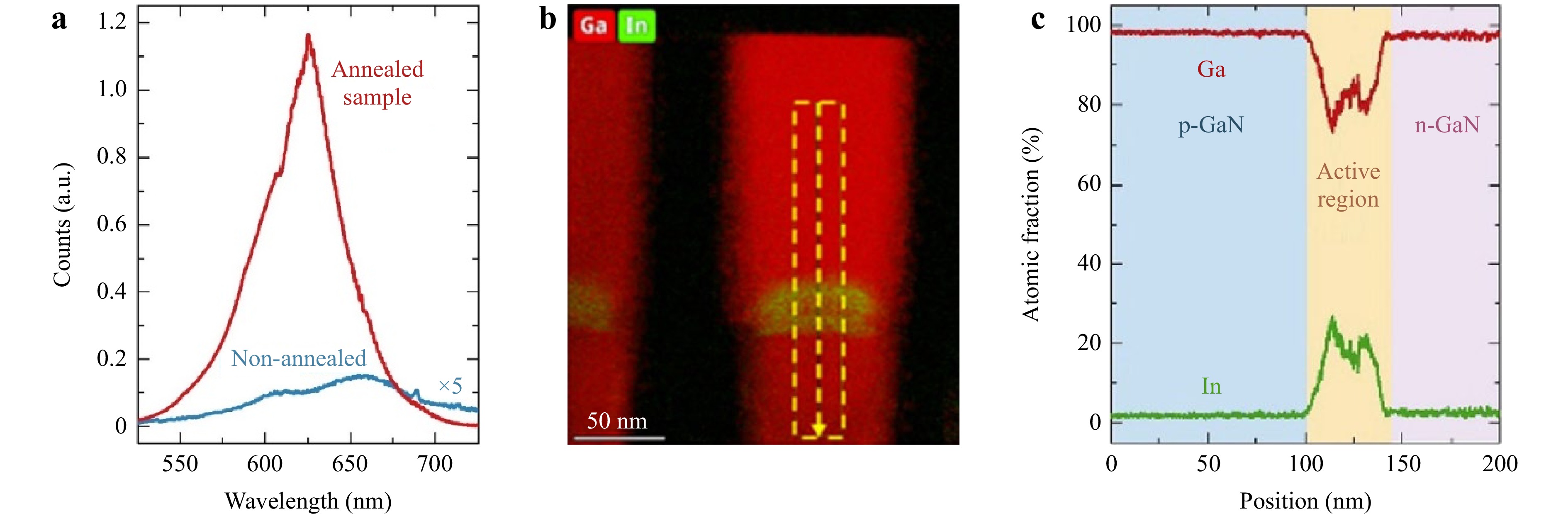
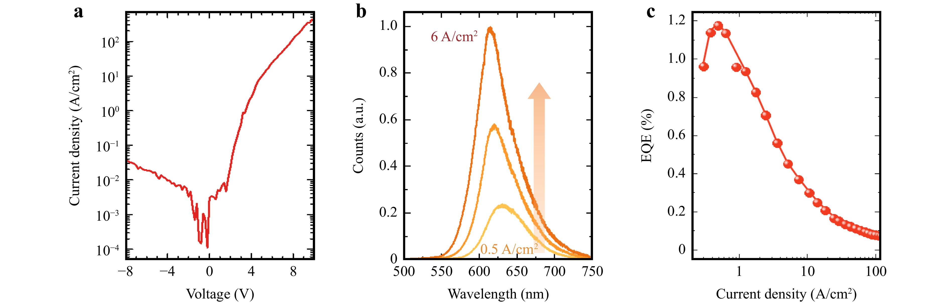
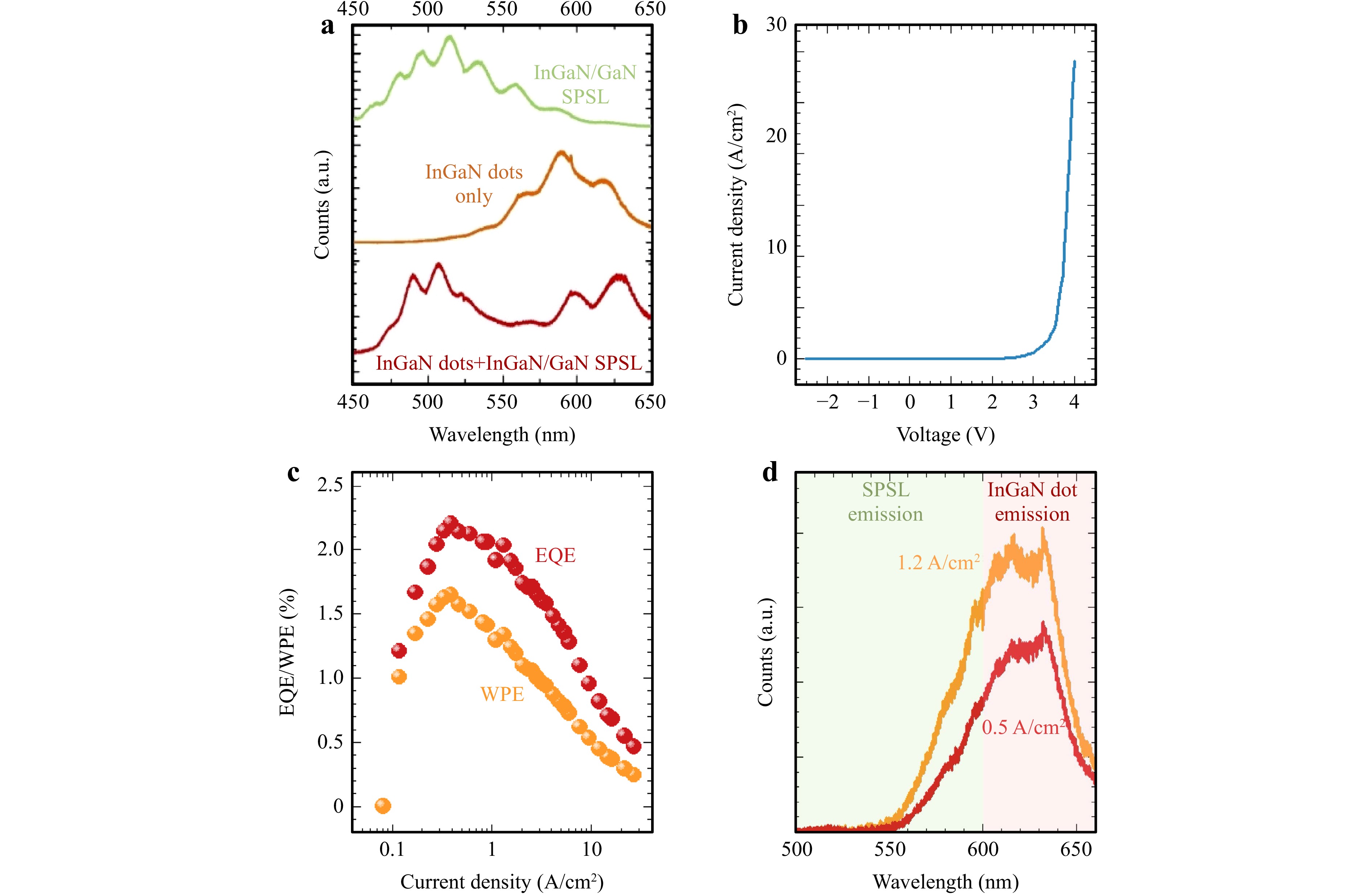
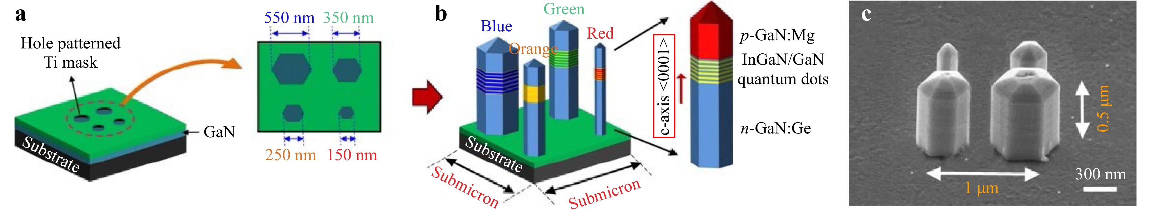
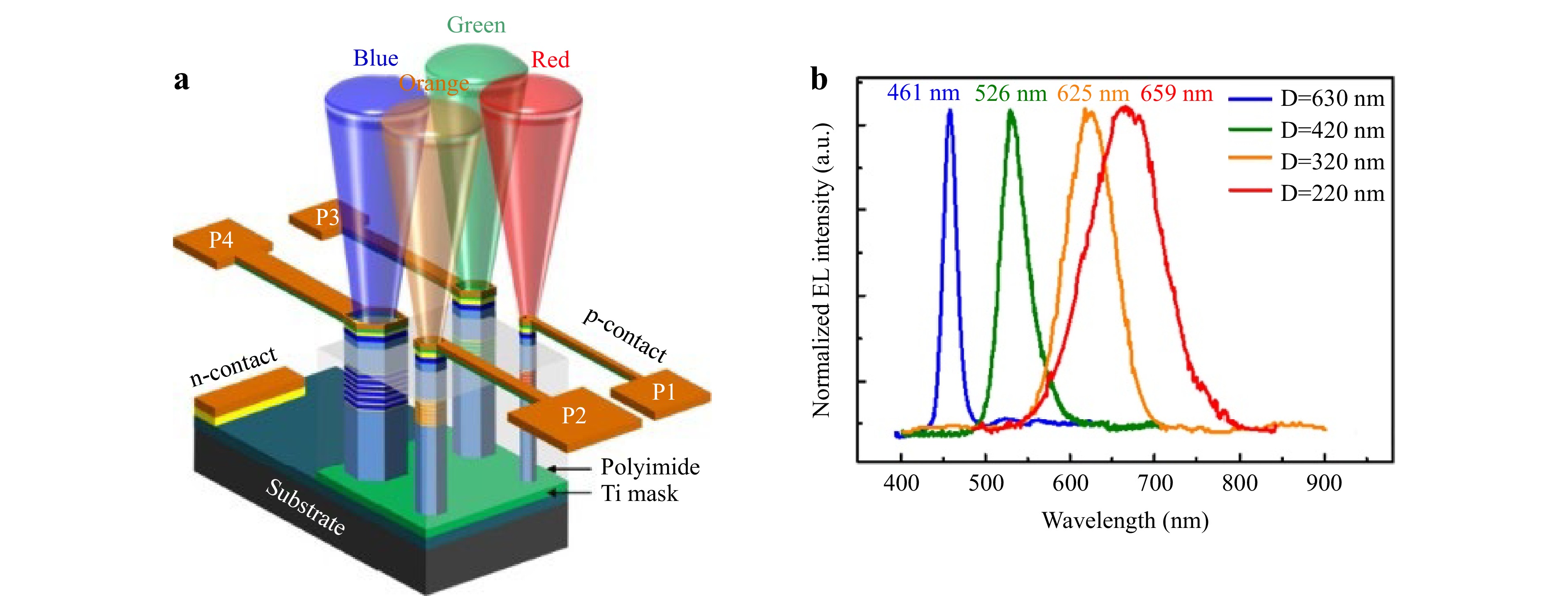
With the advent of technologies such as augmented/virtual reality (AR/VR) that are moving towards displays with high efficiency, small size, and ultrahigh resolution, the development of optoelectronic devices with scales on the order of a few microns or even smaller has attracted considerable interest. In this review article we provide an overview of some of the recent developments of visible micron-scale light emitting diodes (LEDs). The major challenges of higher surface recombination for smaller size devices, the difficulty in attaining longer emission wavelengths, and the complexity of integrating individual, full color devices into a display are discussed, along with techniques developed to address them. We then present recent work on bottom-up nanostructure-based sub-micron LEDs, highlighting their unique advantages, recent developments, and promising potential. Finally, we present perspectives for future development of micro-LEDs for higher efficiencies, better color output and more efficient integration.
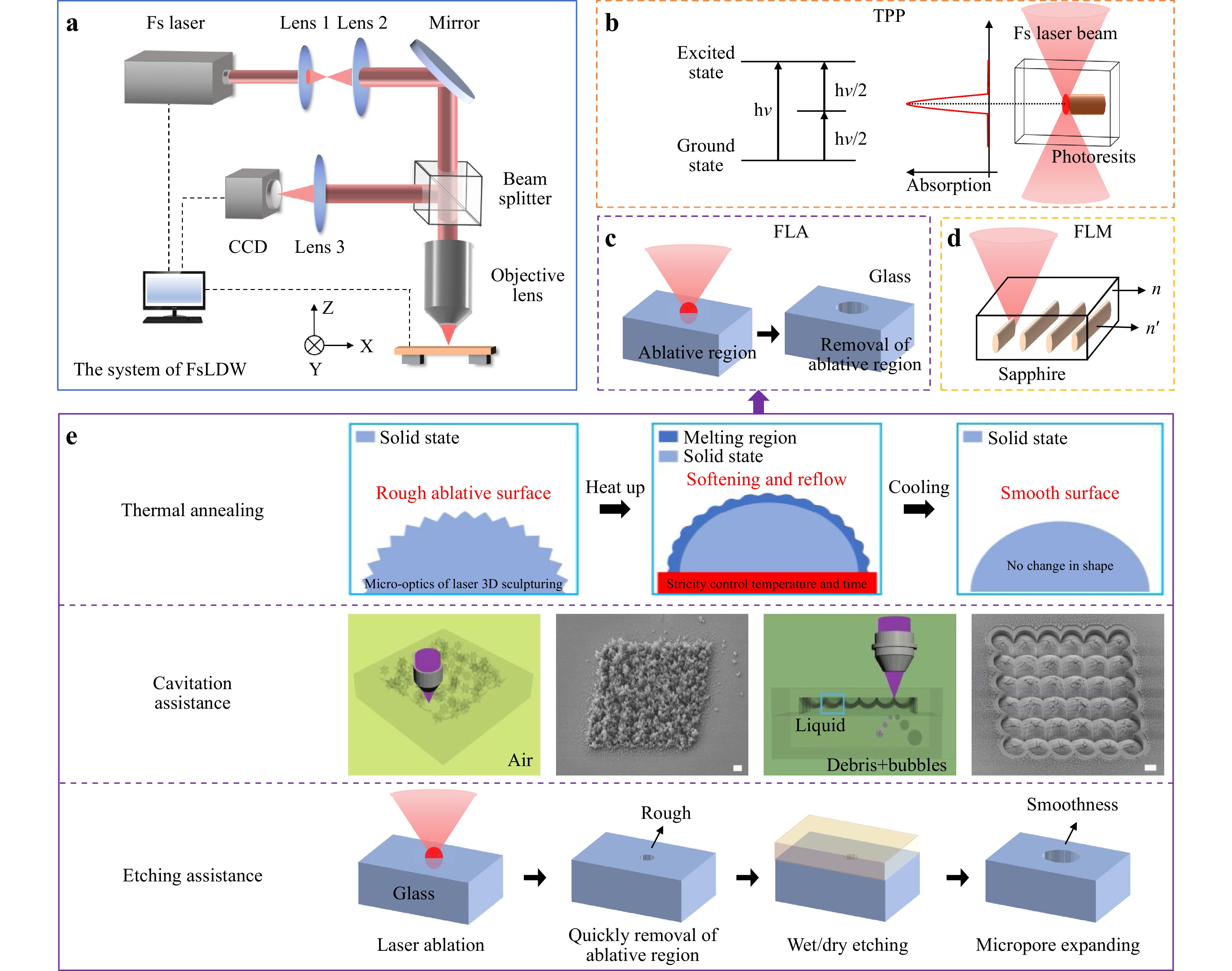
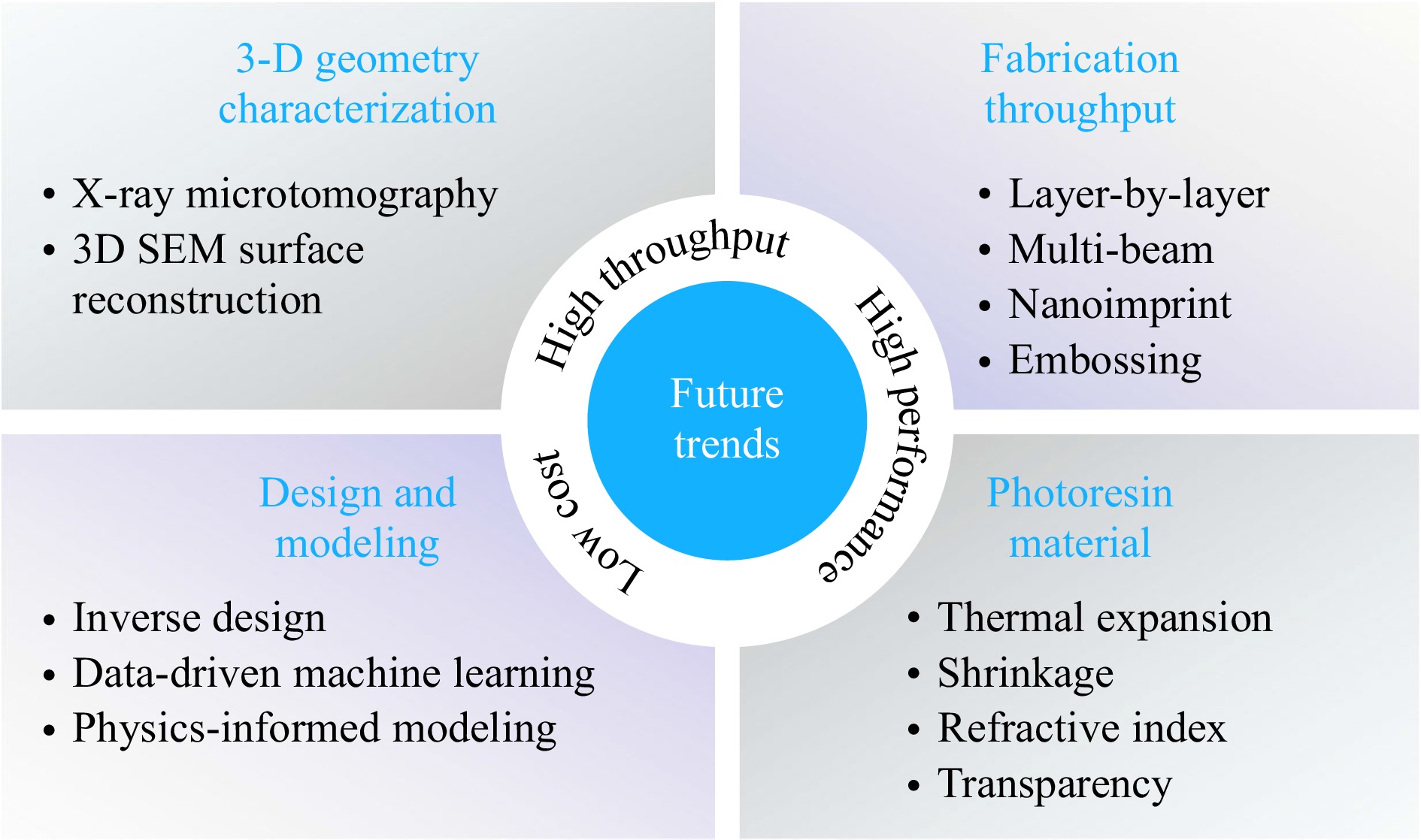
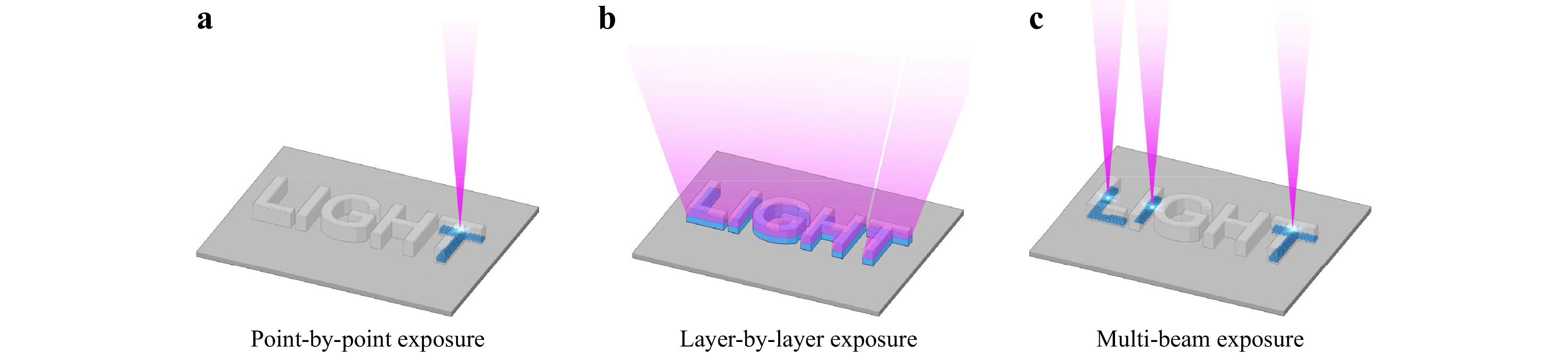
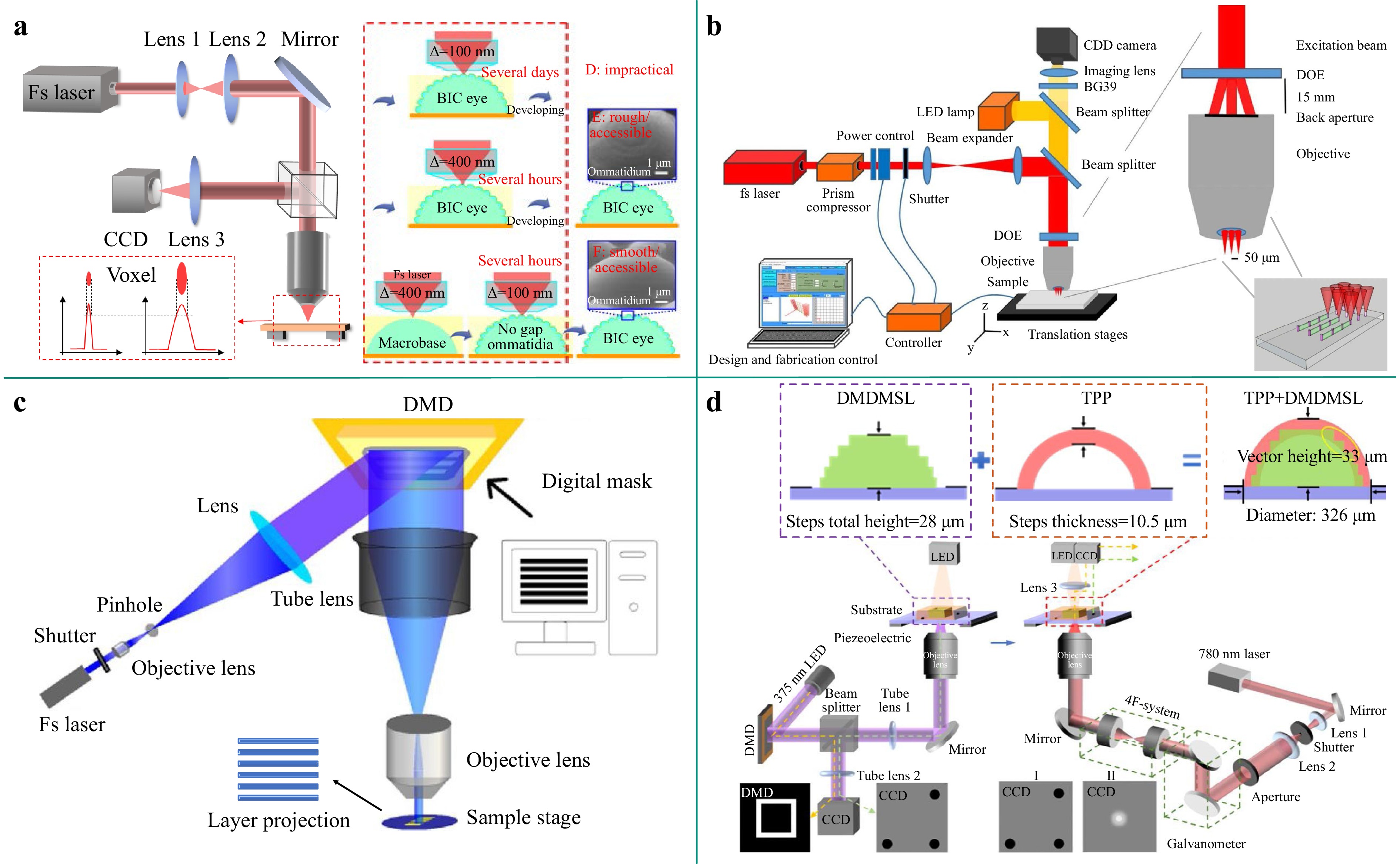
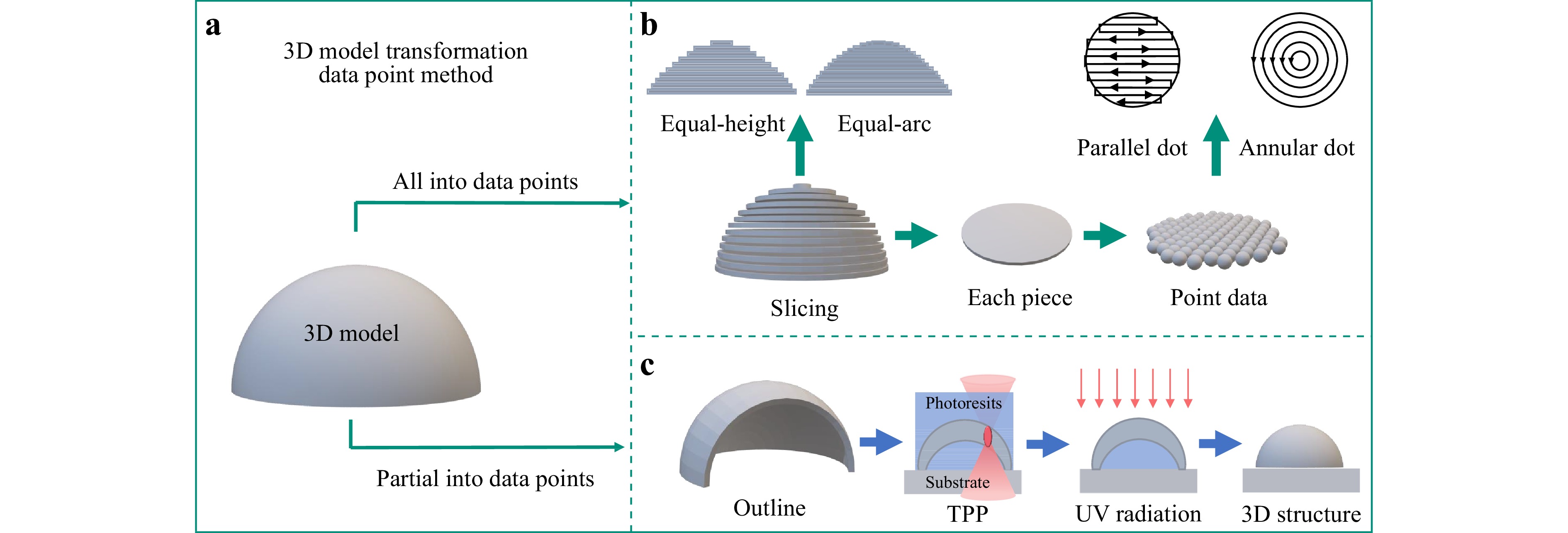
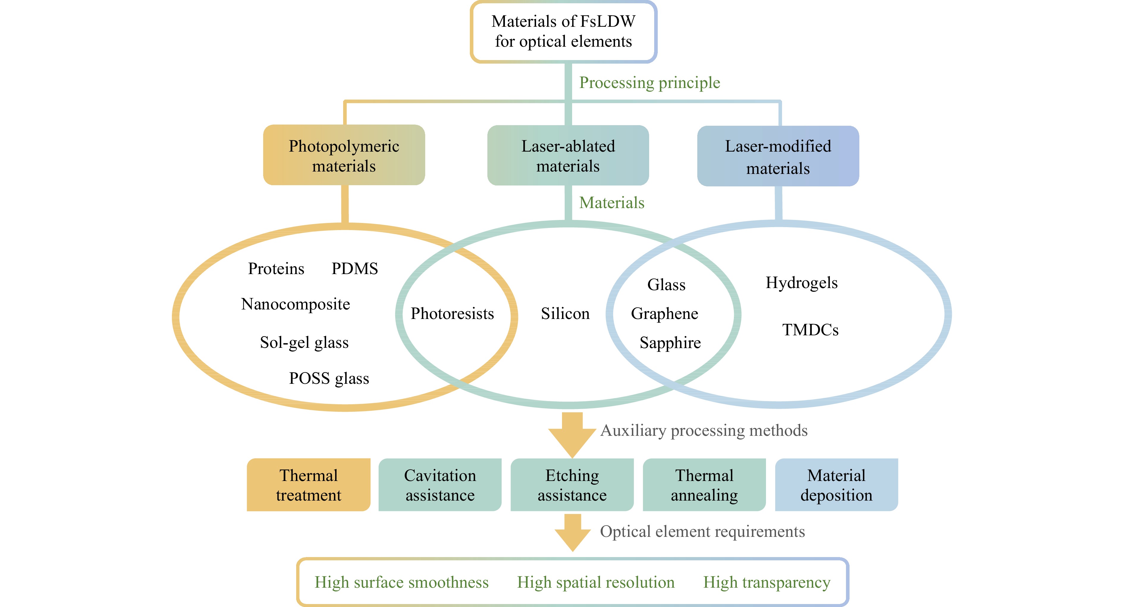
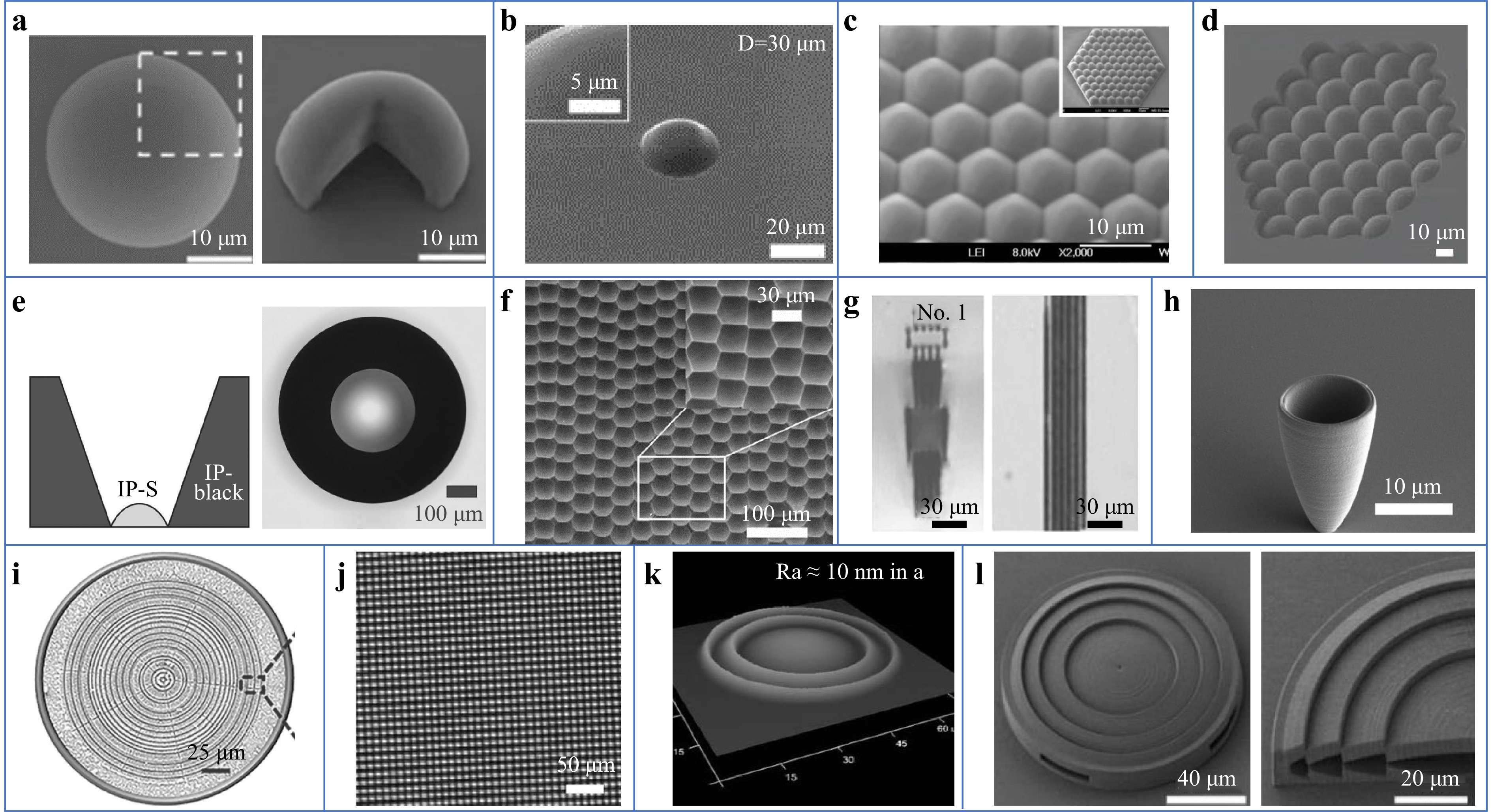
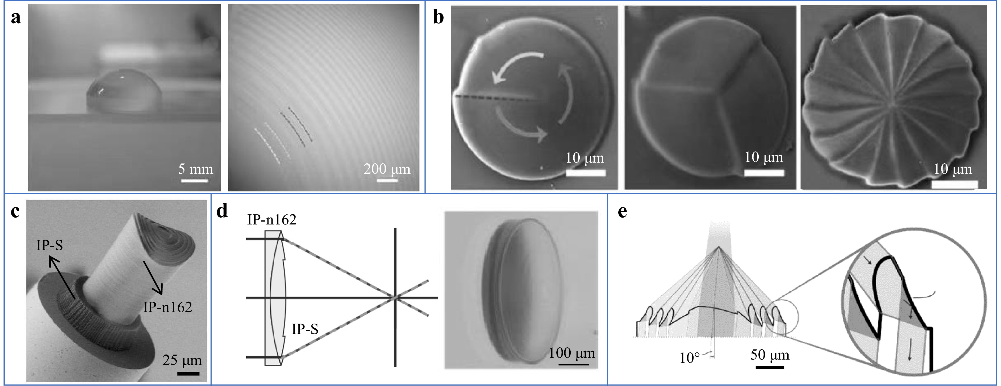
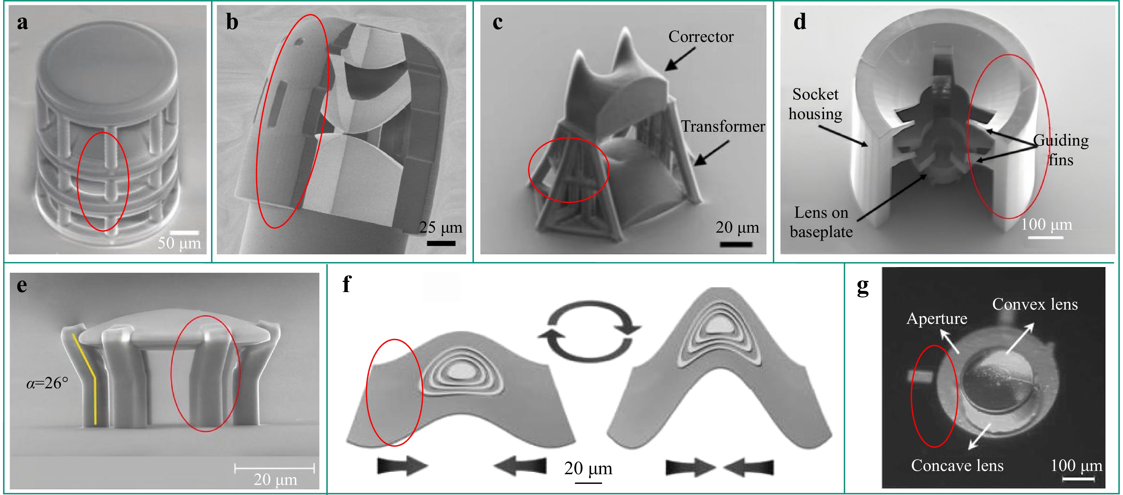
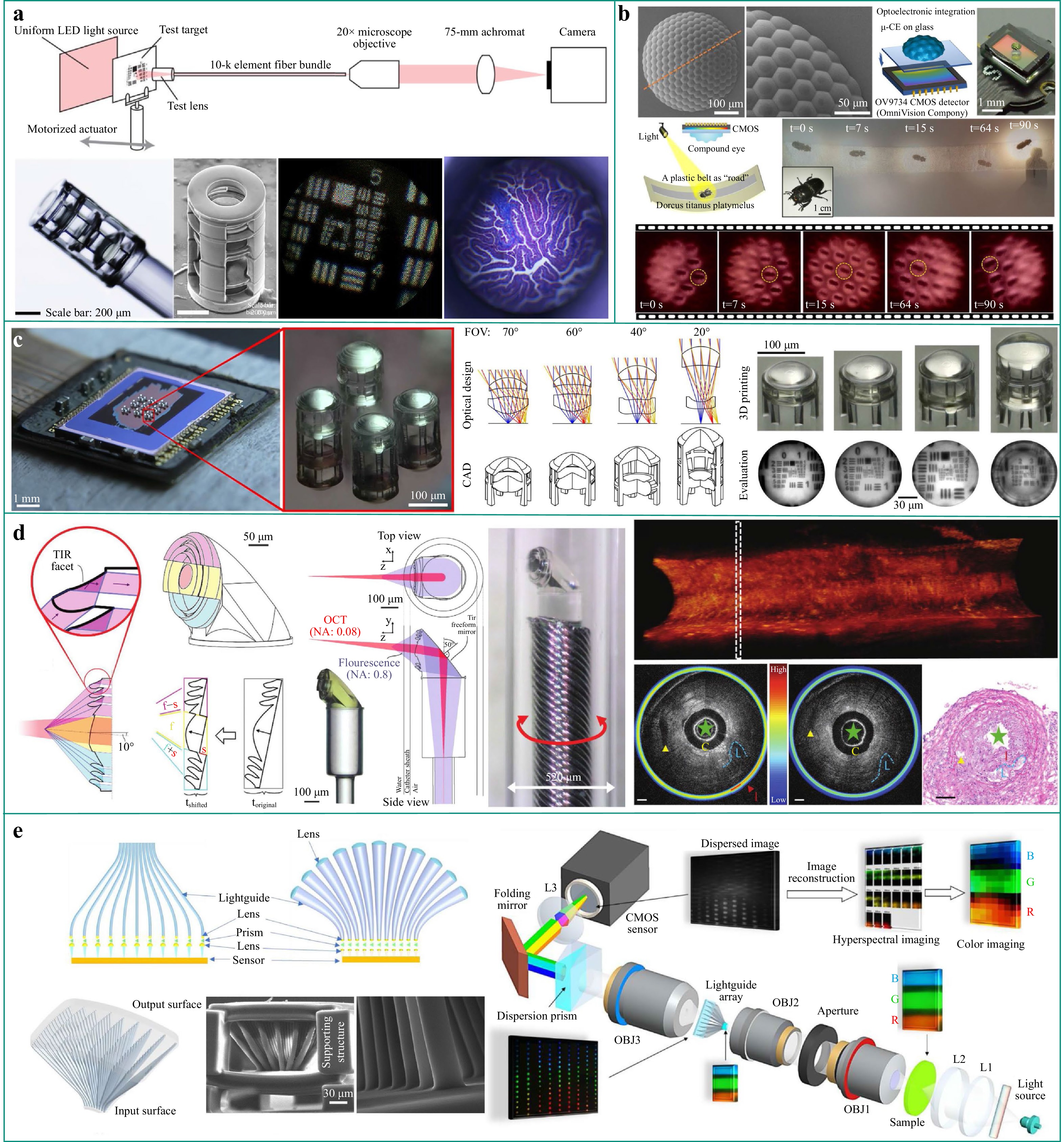
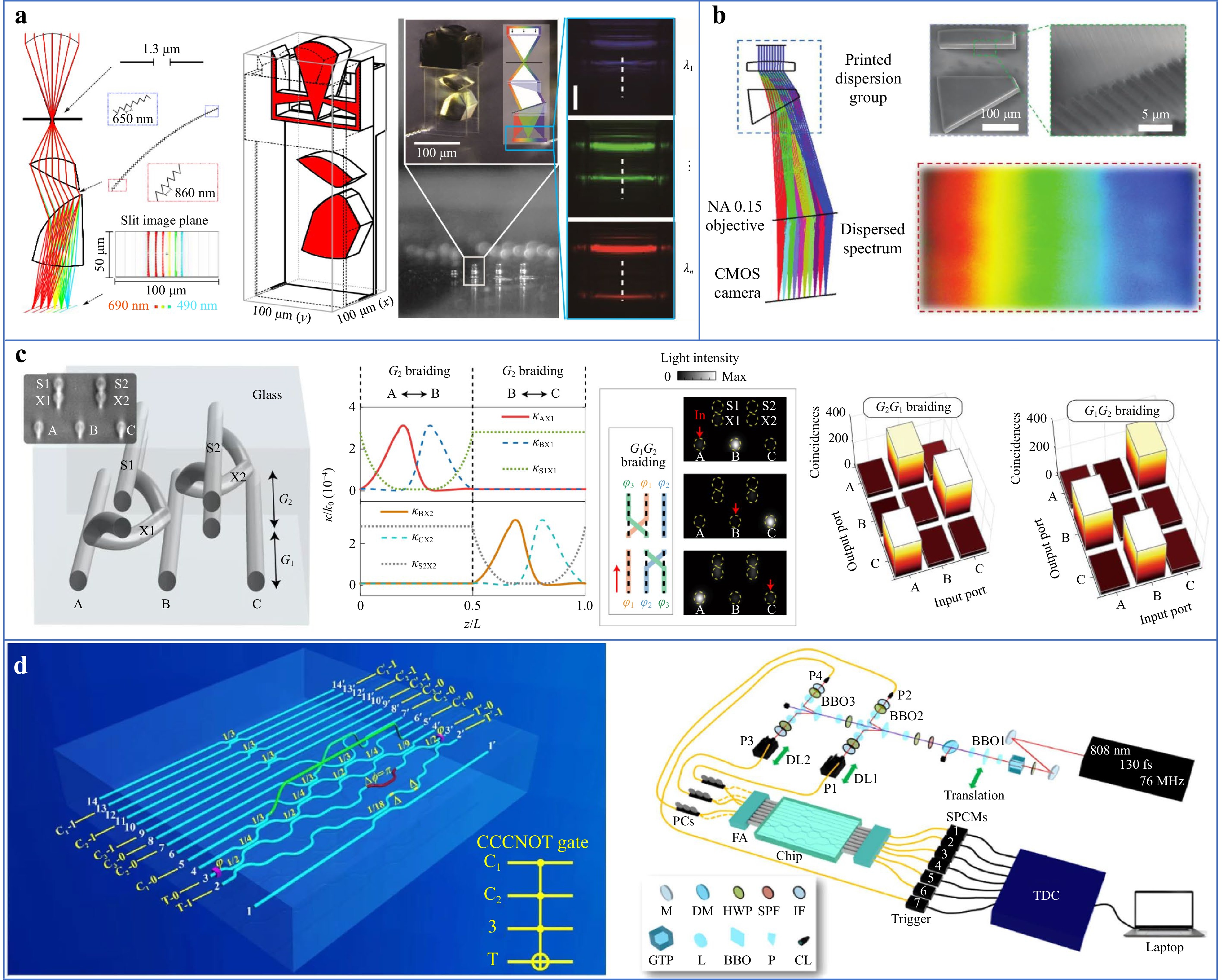
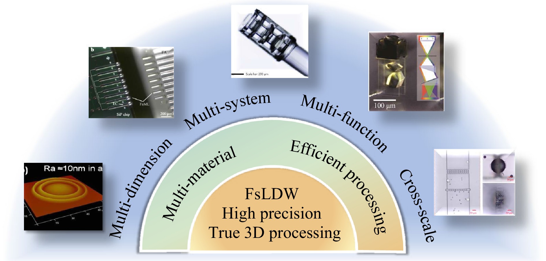
The development of modern information technology has led to significant demand for microoptical elements with complex surface profiles and nanoscale surface roughness. Therefore, various micro- and nanoprocessing techniques are used to fabricate microoptical elements and systems. Femtosecond laser direct writing (FsLDW) uses ultrafast pulses and the ultraintense instantaneous energy of a femtosecond laser for micro-nano fabrication. FsLDW exhibits various excellent properties, including nonlinear multiphoton absorption, high-precision processing beyond the diffraction limit, and the universality of processable materials, demonstrating its unique advantages and potential applications in three-dimensional (3D) micro-nano manufacturing. FsLDW has demonstrated its value in the fabrication of various microoptical systems. This study details three typical principles of FsLDW, several design considerations to improve processing performance, processable materials, imaging/nonimaging microoptical elements, and their stereoscopic systems. Finally, a summary and perspective on the future research directions for FsLDW-enabled microoptical elements and stereoscopic systems are provided.

 Email
Email RSS
RSS