
Special Issue | 17 December 2025
Special Issue on Extreme Manufacturing

Extreme Manufacturing refers to the fabrication of structures and devices at the two extremes of the manufacturing scale: from a nanometer to a meter. Light sources, such as lasers, have emerged as key tools at the forefront of this field, enabling the possibility of ultrahigh-precision and high speed manufacturing. Light-based techniques contain additive and subtractive manufacturing, facilitating the creation of ultra-high-resolution structures and high-performance devices. Recent advances in light-based additive and subtractive manufacturing have further expanded the capabilities of Extreme Manufacturing, enabling ultra-high resolution rapid prototyping and serial fabrication of complex designs, the fabrication of intricate geometries, and the development of novel materials with tailored properties. The emerging progress made in Extreme Manufacturing thus paves the way for the generation of cutting-edge applications across a wide range of fields, including photonics, optics, mechanics, sensing, imaging, energy conversion, tissue engineering, regenerative medicine, and more.
This special issue is to provide the most exciting advances in the field of light based extreme manufacturing and its applications, including new materials, fabrication and characterization technologies, novel micro- and nanodevices in optics and photonics, microfluidics, and architected materials and so on. We hope to provide an overview as well as insightful perspectives of this field by collecting the cutting-edge achievements from international researchers in the community and promote scientific breakthroughs and practical prospects of extreme manufacturing with light.
This issue is co-edited by
Prof. Dong Wu, University of Science and Technology of China, China
Prof. Liang Yang, University of Science and Technology of China, China
Prof. Mangirdas Malinauskas, Vilnius University, Lithuania
Prof. Maria Farsari, The Institute of Electronic Structure and Laser of the Foundation for Research and Technology-Hellas (IESL-FORTH), Greece
Dr. Gordon Zyla, The Institute of Electronic Structure and Laser of the Foundation for Research and Technology-Hellas (IESL-FORTH), Greece
Dr. Patrick Salter, University of Oxford, UK
-
Article
A shoe-box-sized 3D laser nanoprinter based on two-step absorption
 Published , Published online: 09 July 2024 , doi: 10.37188/lam.2024.027
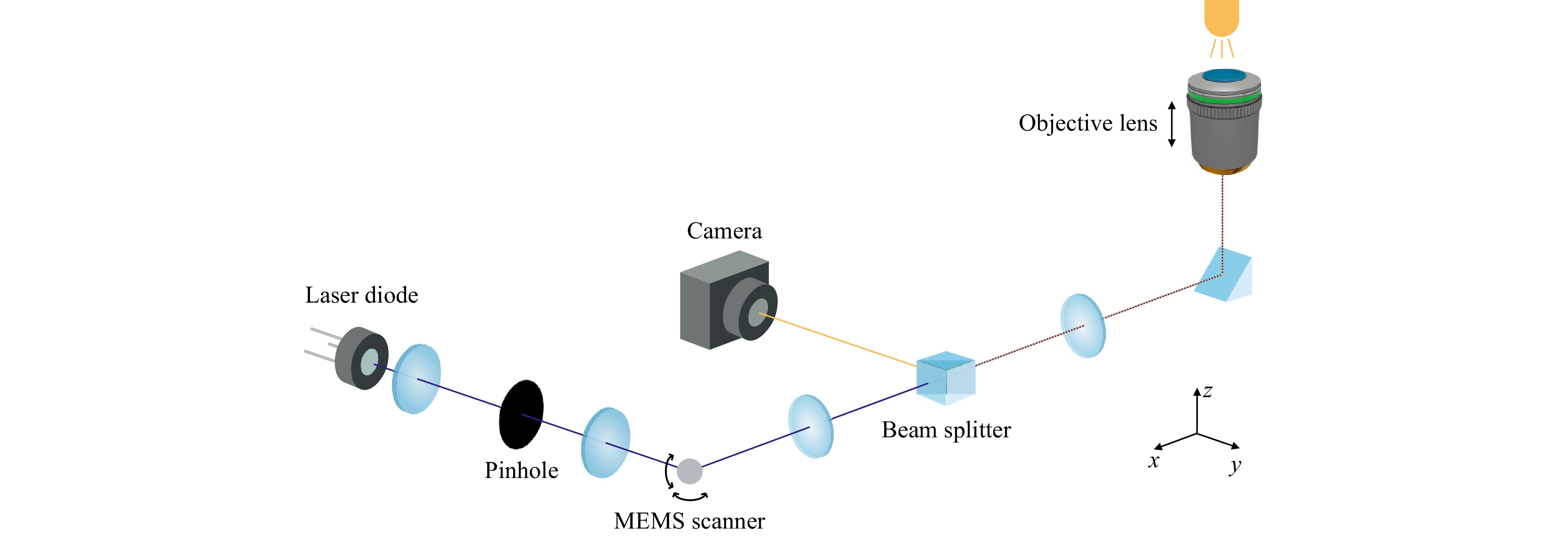
State-of-the-art commercially available 3D laser micro- and nanoprinters using polymeric photoresists based on two- or multi-photon absorption rely on high-power pico- or femtosecond lasers, leading to fairly large and expensive instruments. Lately, we have introduced photoresists based on two-step absorption instead of two-photon absorption, allowing for the use of small and inexpensive continuous-wave 405 nm wavelength GaN semiconductor laser diodes with light-output powers below 1 mW. Here, using the identical photoresist system and similar laser diodes, we report on the design, construction, and characterization of a 3D laser nanoprinter that fits into a shoe box. This shoe box contains all optical components, namely the mounted laser, the collimation- and beam-shaping optics, a miniature MEMS xy-scanner, a tube lens, the focusing microscope objective lens (NA=1.4, 100× magnification), a piezo slip-stick z-stage, the sample holder, a camera monitoring system, LED sample illumination, as well as the miniaturized control electronics employing a microcontroller. We present a gallery of example 3D structures printed with this instrument. We achieve about 100 nm lateral spatial resolution and focus scan speeds of about 1 mm/s. Potentially, our shoe-box-sized system can be made orders of magnitude less expensive than today’ s commercial systems.
-
Article
A multi-photon (7 × 7)-focus 3D laser printer based on a 3D-printed diffractive optical element and a 3D-printed multi-lens array
 Published , Published online: 06 March 2024 , doi: 10.37188/lam.2024.003
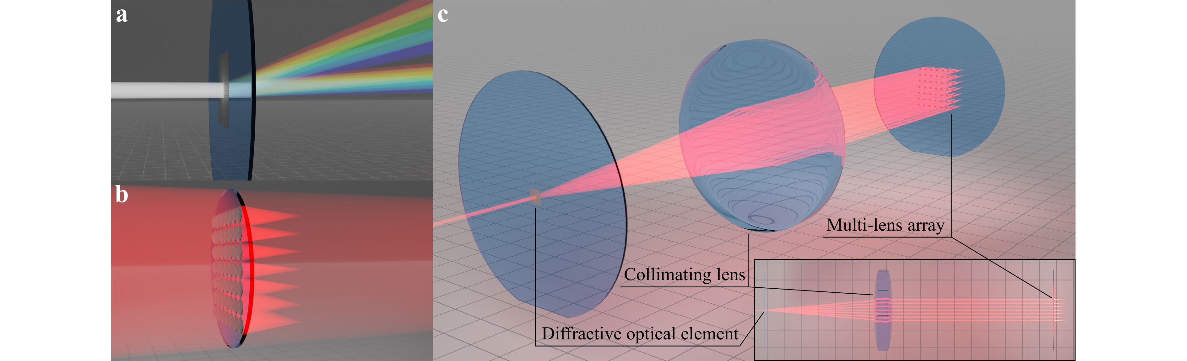
One of the challenges in the field of multi-photon 3D laser printing lies in further increasing the print speed in terms of voxels/s. Here, we present a setup based on a 7 × 7 focus array (rather than 3 × 3 in our previous work) and using a focus velocity of about 1 m/s (rather than 0.5 m/s in our previous work) at the diffraction limit (40×/NA1.4 microscope objective lens). Combined, this advance leads to a ten times increased print speed of about 108 voxels/s. We demonstrate polymer printing of a chiral metamaterial containing more than 1.7 × 10¹² voxels as well as millions of printed microparticles for potential pharmaceutical applications. The critical high-quality micro-optical components of the setup, namely a diffractive optical element generating the 7 × 7 beamlets and a 7 × 7 lens array, are manufactured by using a commercial two-photon grayscale 3D laser printer.
-
Article
Ultrafast laser processing of silk films by bulging and ablation for optical functional devices
 Published , Published online: 12 July 2024 , doi: 10.37188/lam.2024.024
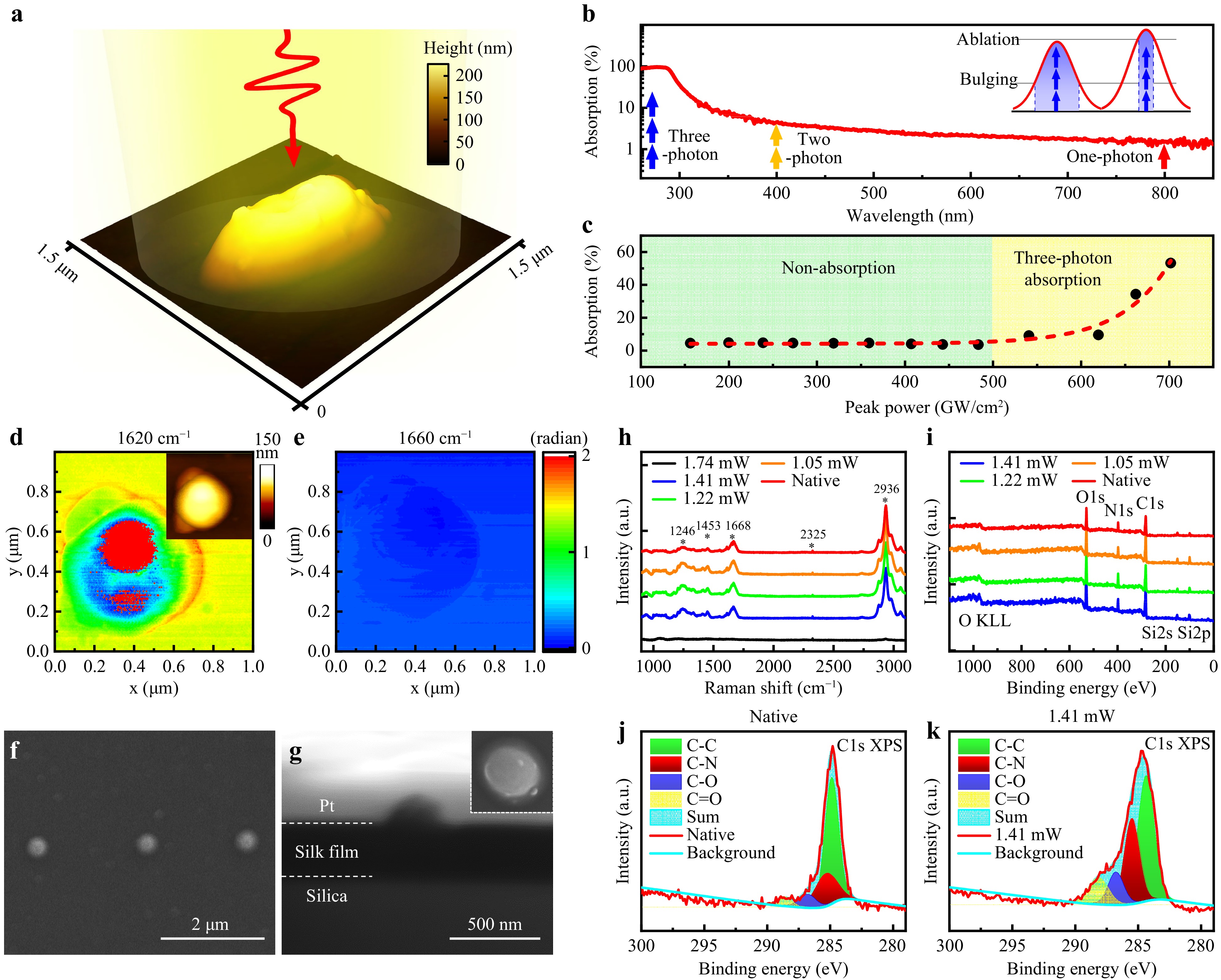
Organic proteins are attractive owing to their unique optical properties, remarkable mechanical characteristics, and biocompatibility. Manufacturing multifunctional structures on organic protein films is essential for practical applications; however, the controllable fabrication of specific structures remains challenging. Herein, we propose a strategy for creating specific structures on silk film surfaces by modulating the bulging and ablation of organic materials. Unique surface morphologies such as bulges and craters with continuously varying diameters were generated based on the controlled ultrafast laser-induced crystal-form transition and plasma ablation of the silk protein. Owing to the anisotropic optical properties of the bulge/crater structures with different periods, the fabricated organic films can be used for large-scale inkless color printing. By simultaneously engineering bulge/crater structures, we designed and demonstrated organic film-based optical functional devices that achieves holographic imaging and optical focusing. This study provides a promising strategy for the fabrication of multifunctional micro/nanostructures that can broaden the potential applications of organic materials.
-
Article
Parallel fabrication of silica optical microfibers and nanofibers
 Published , Published online: 08 July 2024 , doi: 10.37188/lam.2024.020
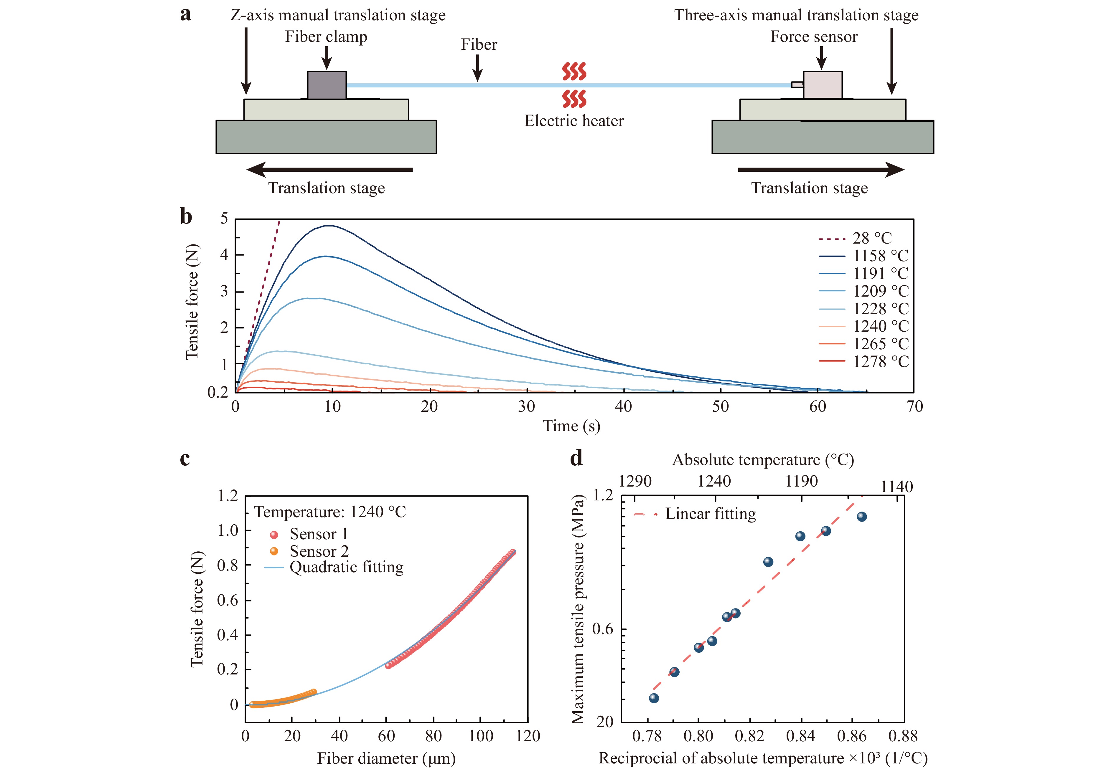
Optical micro/nanofibers (MNFs) taper-drawn from silica fibers possess intriguing optical and mechanical properties. Recently, MNF array or MNFs with identical geometries have been attracting more and more attention, however, current fabrication technique can draw only one MNF at a time, with a low drawing speed (typically 0.1 mm/s) and a complicated process for high-precision control, making it inefficient in fabricating multiple MNFs. Here, we propose a parallel-fabrication approach to simultaneously drawing multiple (up to 20) MNFs with almost identical geometries. For fiber diameter larger than 500 nm, measured optical transmittances of all as-drawn MNFs exceed 96.7% at 1550-nm wavelength, with a diameter deviation within 5%. Our results pave a way towards high-yield fabrication of MNFs that may find applications from MNF-based optical sensors, optical manipulation to fiber-to-chip interconnection.
-
Article
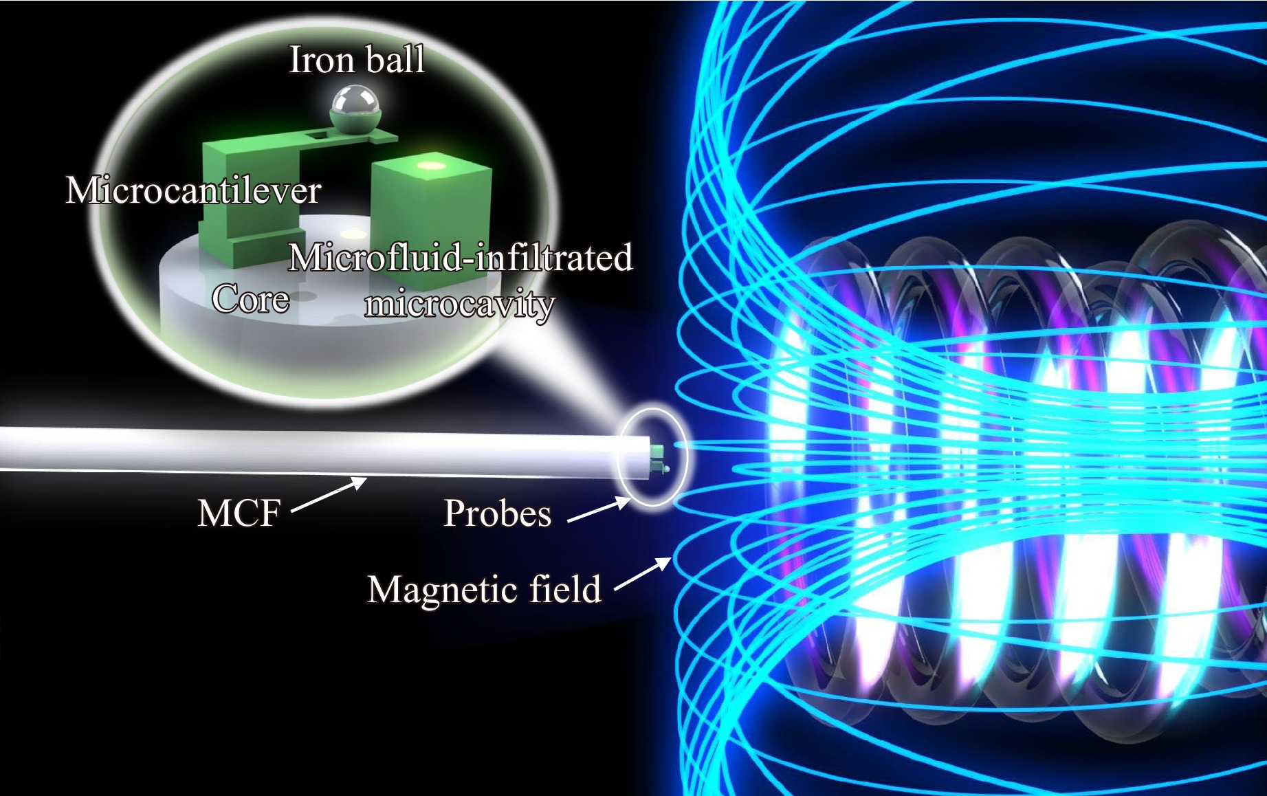
3D printed multicore fiber-tip discriminative sensor for magnetic field and temperature measurements
 Published , Published online: 27 March 2024 , doi: 10.37188/lam.2024.018
Miniaturized fiber-optic magnetic field sensors have attracted considerable interest owing to their superiorities in anti-electromagnetic interference and compactness. However, the intrinsic thermodynamic properties of the material make temperature cross-sensitivity a challenging problem in terms of sensing accuracy and reliability. In this study, an ultracompact multicore fiber (MCF) tip sensor was designed to discriminatively measure the magnetic field and temperature, which was subsequently evaluated experimentally. The novel 3D printed sensing component consists of a bowl-shaped microcantilever and a polymer microfluid-infiltrated microcavity on the end-facet of an MCF, acting as two miniaturized Fabry-Perot interferometers. The magnetic sensitivity of the microcantilever was implemented by incorporating an iron micro ball into the microcantilever, and the microfluid-infiltrated microcavity enhanced the capability of highly sensitive temperature sensing. Using this tiny fiber-facet device in the two channels of an MCF allows discriminative measurements of the magnetic field and temperature by determining the sensitivity coefficient matrix of two parameters. The device exhibited a high magnetic field intensity sensitivity, approximately 1805.6 pm/mT with a fast response time of ~ 213 ms and a high temperature sensitivity of 160.3 pm/℃. Moreover, the sensor had a low condition number of 11.28, indicating high reliability in two-parameter measurements. The proposed 3D printed MCF-tip probes, which detect multiple signals through multiple channels within a single fiber, can provide an ultracompact, sensitive, and reliable scheme for discriminative measurements. The bowl-shaped microcantilever also provides a useful platform for incorporating microstructures with functional materials, extending multi-parameter sensing scenarios and promoting the application of MCFs.
-
Article
Light focusing and additive manufacturing through highly scattering media using upconversion nanoparticles
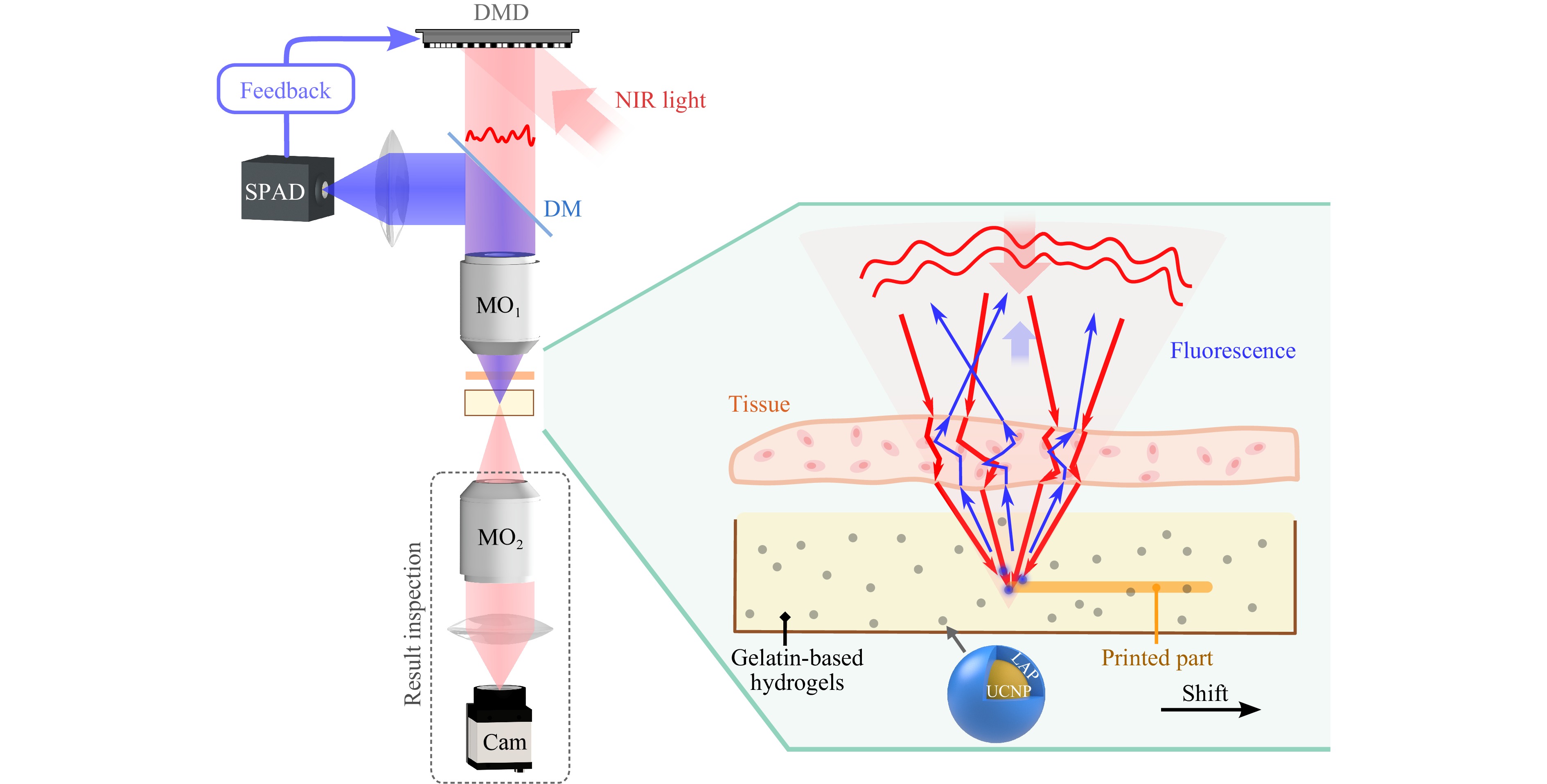 Published , Published online: 03 April 2025 , doi: 10.37188/lam.2025.021Light-based additive manufacturing holds great potential in the field of bioprinting due to its exceptional spatial resolution, enabling the reconstruction of intricate tissue structures. However, printing through biological tissues is severely limited due to the strong optical scattering within the tissues. The propagation of light is scrambled to form random speckle patterns, making it impossible to print features at the diffraction-limited size with conventional printing approaches. The poor tissue penetration depth of ultra-violet or blue light, which is commonly used to trigger photopolymerization, further limits the fabrication of high cell-density tissue constructs. Recently, several strategies based on wavefront shaping have been developed to manipulate the light and refocus it inside scattering media to a diffraction-limited spot. In this study, we present a high-resolution additive manufacturing technique using upconversion nanoparticles and a wavefront shaping method that does not require measurement from an invasive detector, i.e., it is a non-invasive technique. Upconversion nanoparticles convert near-infrared light to ultraviolet and visible light. The ultraviolet light serves as a light source for photopolymerization and the visible light as a guide star for digital light shaping. The incident light pattern is manipulated using the feedback information of the guide star to focus light through the tissue. In this way, we experimentally demonstrate that near-infrared light can be non-invasively focused through a strongly scattering medium. By exploiting the optical memory effect, we further demonstrate micro-meter resolution additive manufacturing through highly scattering media such as a 300-μm-thick chicken breast. This study provides a concept of high-resolution additive manufacturing through turbid media with potential application in tissue engineering.
 -
Article
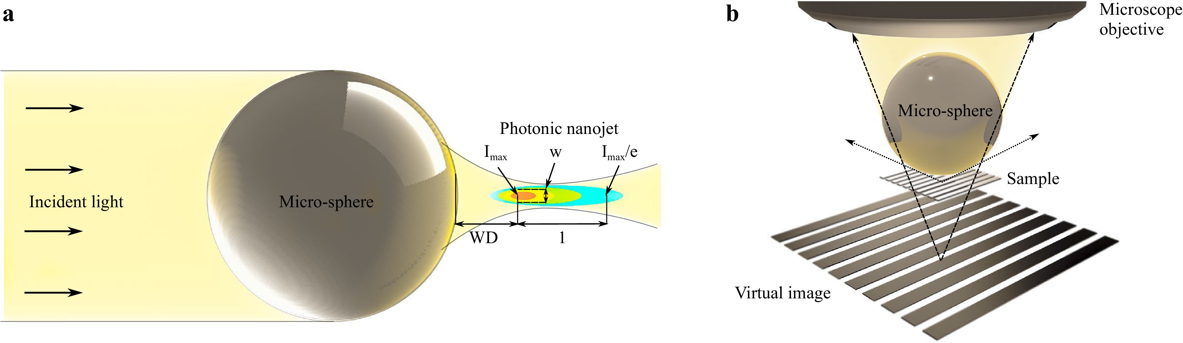
3D micro-devices for enhancing the lateral resolution in optical microscopy
 Published , Published online: 28 May 2024 , doi: 10.37188/lam.2024.019
Although optical microscopy is a widely used technique across various multidisciplinary fields for inspecting small-scale objects, surfaces or organisms, it faces a significant limitation: the lateral resolution of optical microscopes is fundamentally constrained by light diffraction. Dielectric micro-spheres, however, offer a promising solution to this issue as they are capable of significantly enhancing lateral resolution through extraordinary phenomena, such as a photonic nanojet.Building upon the potential of dielectric micro-spheres, this paper introduces a novel approach for fabricating 3D micro-devices designed to enhance lateral resolution in optical microscopy. The proposed 3D micro-device comprises a modified coverslip and a micro-sphere, facilitating easy handling and integration into any existing optical microscope. To manufacture the device, two advanced femtosecond laser techniques are employed: femtosecond laser ablation and multi-photon lithography. Femtosecond laser ablation was employed to create a micro-hole in the coverslip, which allows light to be focused through this aperture. Multi-photon lithography was used to fabricate a micro-sphere with a diameter of 20 µm, along with a cantilever that positions the above the processed micro-hole and connect it with the coverslip. In this context, advanced processing strategies for multi-photon lithography to produce a micro-sphere with superior surface roughness and almost perfect geometry (λ/8) from a Zr-based hybrid photoresist are demonstrated. The performance of the micro-device was evaluated using Mirau-type coherence scanning interferometry in conjunction with white light illumination at a central wavelength of 600 nm and a calibration grid (Λ = 0.28 µm, h > 50 nm). Here, the 3D micro-device proved to be capable of enhancing lateral resolution beyond the limits achievable with conventional lenses or microscope objectives when used in air. Simultaneously, it maintained the high axial resolution characteristic of Mirau-type coherence scanning interferometry. The results and optical properties of the micro-sphere were analyzed and further discussed through simulations.
-
Article
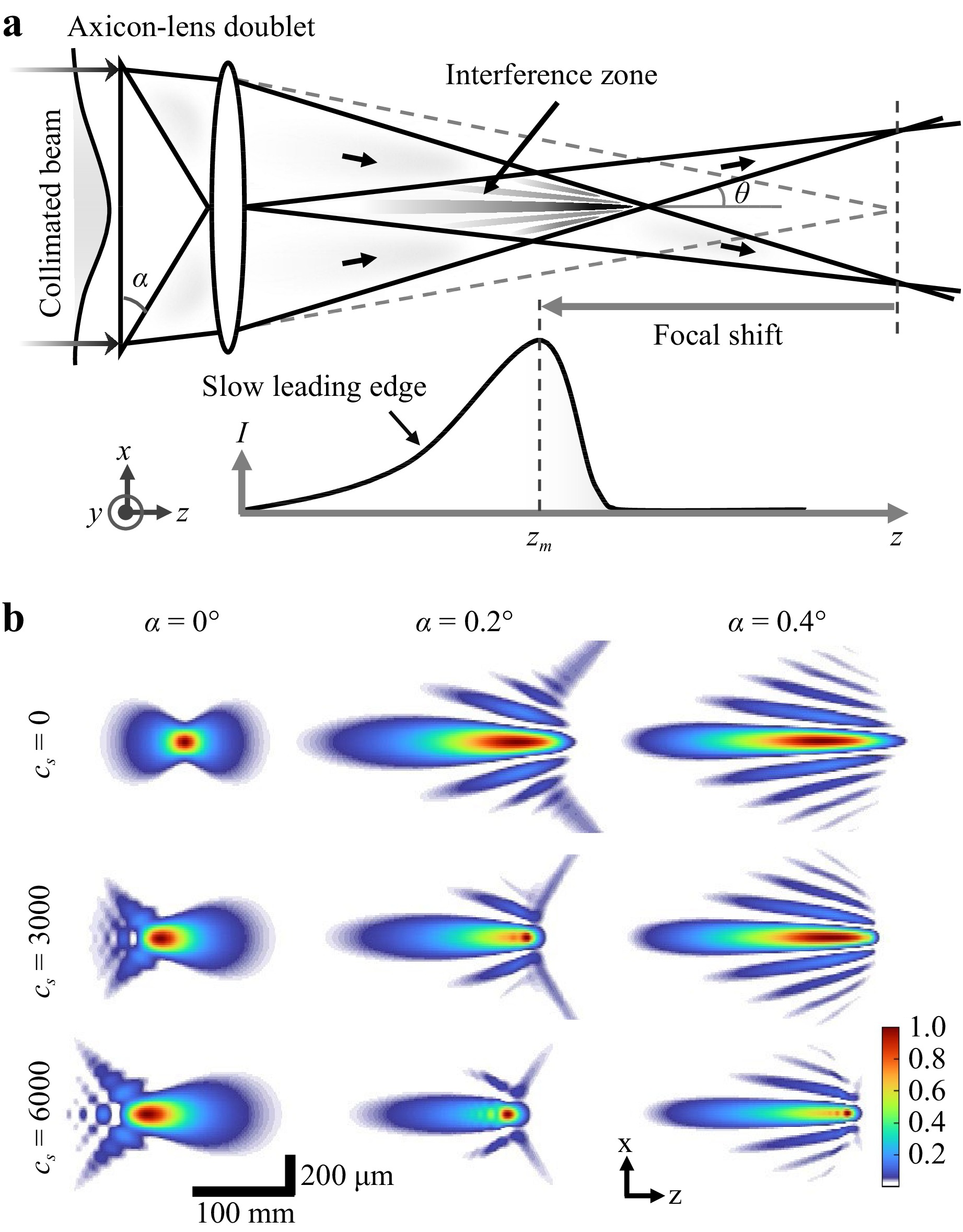
Ultra-high-aspect-ratio structures through silicon using infrared laser pulses focused with axicon-lens doublets
 Published , Published online: 10 July 2024 , doi: 10.37188/lam.2024.022
We describe how a direct combination of an axicon and a lens can represent a simple and efficient beam-shaping solution for laser material processing applications. We produce high-angle pseudo-Bessel micro-beams at 1550 nm, which would be difficult to produce by other methods. Combined with appropriate stretching of femtosecond pulses, we access optimized conditions inside semiconductors allowing us to develop high-aspect-ratio refractive-index writing methods. Using ultrafast microscopy techniques, we characterize the delivered local intensities and the triggered ionization dynamics inside silicon with 200-fs and 50-ps pulses. While similar plasma densities are produced in both cases, we show that repeated picosecond irradiation induces permanent modifications spontaneously growing shot-after-shot in the direction of the laser beam from front-surface damage to the back side of irradiated silicon wafers. The conditions for direct microexplosion and microchannel drilling similar to those today demonstrated for dielectrics still remain inaccessible. Nonetheless, this work evidences higher energy densities than those previously achieved in semiconductors and a novel percussion writing modality to create structures in silicon with aspect ratios exceeding ~700 without any motion of the beam. The estimated transient change of conductivity and measured ionization fronts at near luminal speed along the observed microplasma channels support the vision of vertical electrical connections optically controllable at GHz repetition rates. The permanent silicon modifications obtained by percussion writing are light-guiding structures according to a measured positive refractive index change exceeding 10−2. These findings open the door to unique monolithic solutions for electrical and optical through-silicon-vias which are key elements for vertical interconnections in 3D chip stacks.
-
Article
High throughput direct writing of a mesoscale binary optical element by femtosecond long focal depth beams
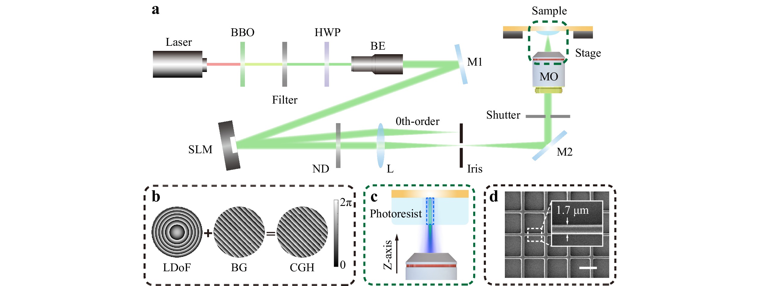 Published , Published online: 17 December 2023 , doi: 10.37188/lam.2023.042
Bessel beams have multiple applications owing to their propagation-invariant properties, including particle trapping, optical coherence tomography, and material processing. However, traditional Bessel-beam shaping techniques require bulky components, which limits the development of miniaturized optical systems for integration with other devices. Here, we report a novel femtosecond laser direct writing strategy for fabricating mesoscale (from submicrometer to subcentimeter) binary optical elements with microscale resolution. This strategy utilizes femtosecond beams with a long focal depth to increase throughput while reducing the constraints on critical sample positioning. As a demonstration, we manufactured and characterized a 2.2 mm diameter binary axicon. The experimentally measured quasi-Bessel beam intensity distribution and the numerical results were remarkably consistent, demonstrating a suitable tradeoff between the overall size, efficiency, and structural fidelity. Furthermore, a compact Bessel lens containing binary axicons was constructed and successfully used for femtosecond laser mask-less ablation of periodic grating-type surface plasmon polariton excitation units. The demonstrated approach shows significant potential for fabricating customizable integrated optical components.
-
Article
In-situ real-time monitoring of ultrafast laser processing using wide-field high-resolution snapshot compressive microscopy
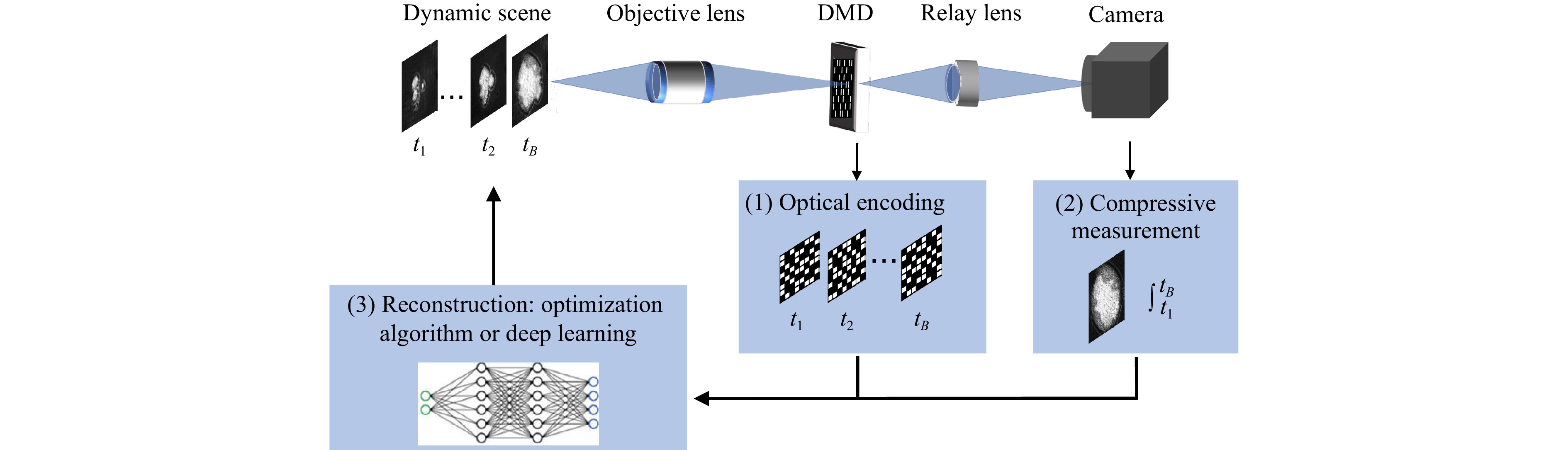 Published , Published online: 15 July 2024 , doi: 10.37188/lam.2024.029
Over the last few decades, ultrafast laser processing has become a widely used tool for manufacturing microstructures and nanostructures. The real-time monitoring of laser material processing provides opportunities to inspect processes and provide feedback. To date, in-situ and real-time monitoring of laser material processing has rarely been performed. To this end, we propose dual-path snapshot compressive microscopy (DP-SCM) for high-speed, large field-of-view, and high-resolution imaging for in-situ and real-time ultrafast laser processing. In the evaluation of DP-SCM, the field of view, lateral resolution, and imaging speed were measured to be 2 mm, 775 nm, and 500 fps, respectively. In ultrafast laser processing, the laser scanning process is observed using a DP-SCM system when translating the sample stage and scanning the focused femtosecond laser. Finally, we monitored the development of a self-organized nanograting structure to validate the potential of our system for unveiling new material mechanisms. The proposed method serves as an add-up (plug-and-play) module for any imaging setup and has vast potential for opening new avenues for high-throughput imaging in laser material processing.
-
Article
Glycerol-assisted grain modulation in femtosecond-laser-induced photochemical synthesis of patterned ZnO nanomaterials
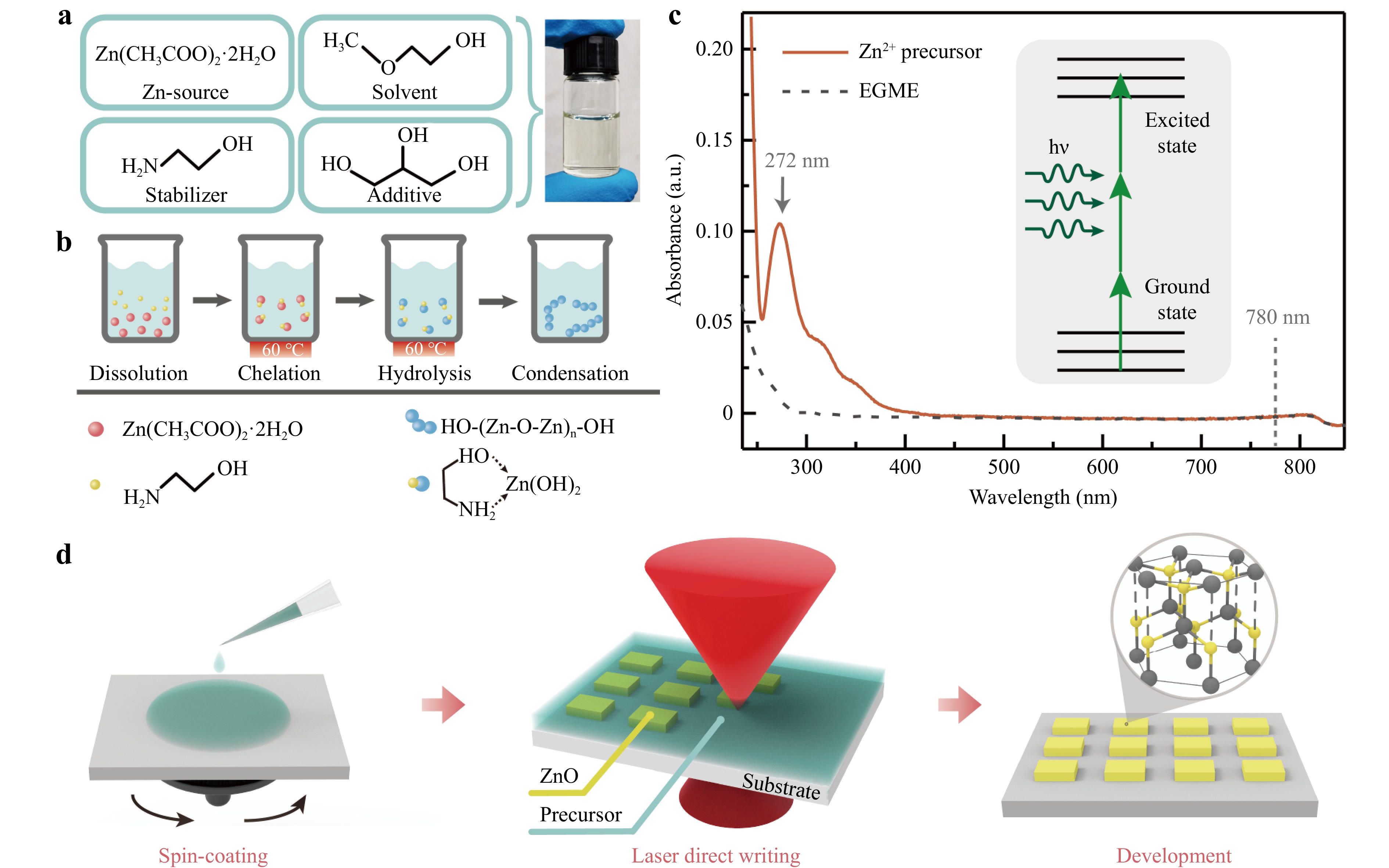 Published , Published online: 07 March 2025 , doi: 10.37188/lam.2025.007
ZnO nanomaterials have become appealing for next-generation micro/nanodevices owing to their remarkable functionality and outstanding performance. However, in-situ, one-step, patterned synthesis of ZnO nanomaterials with small grain sizes and high specific surface areas remains challenging. While breakthroughs in laser-based synthesis techniques have enabled simultaneous growth and patterning of these materials, device integration restrictions owing to pre-prepared laser-absorbing layers remain a severe issue. Herein, we report a single-step femtosecond laser direct writing (FsLDW) method for fabricating ZnO nanomaterial micropatterns with a minimum linewidth of less than 1 μm without requiring laser-absorbing layers. Furthermore, utilizing the grain-size modulation effect of glycerol, we successfully reduced the grain size and addressed the challenges of discontinuity and non-uniform product formation during FsLDW. Using this technique, we successfully fabricated a series of micro-photodetectors with exceptional performance, a switching ratio of 105, and a responsivity of 102 A/W. Notably, the devices exhibited an ultralow dark current of less than 10 pA, more than one order of magnitude lower than the dark current of ZnO photodetectors under the same bias voltage—crucial for enhancing the signal-to-noise ratio and reducing the power consumption of photodetectors. The proposed method could be extended to preparing other metal-oxide nanomaterials and devices, thus providing new opportunities for developing customized, miniaturized, and integrated functional devices.
-
Article
Ultrafast laser-induced decomposition for selective activation of GaAs
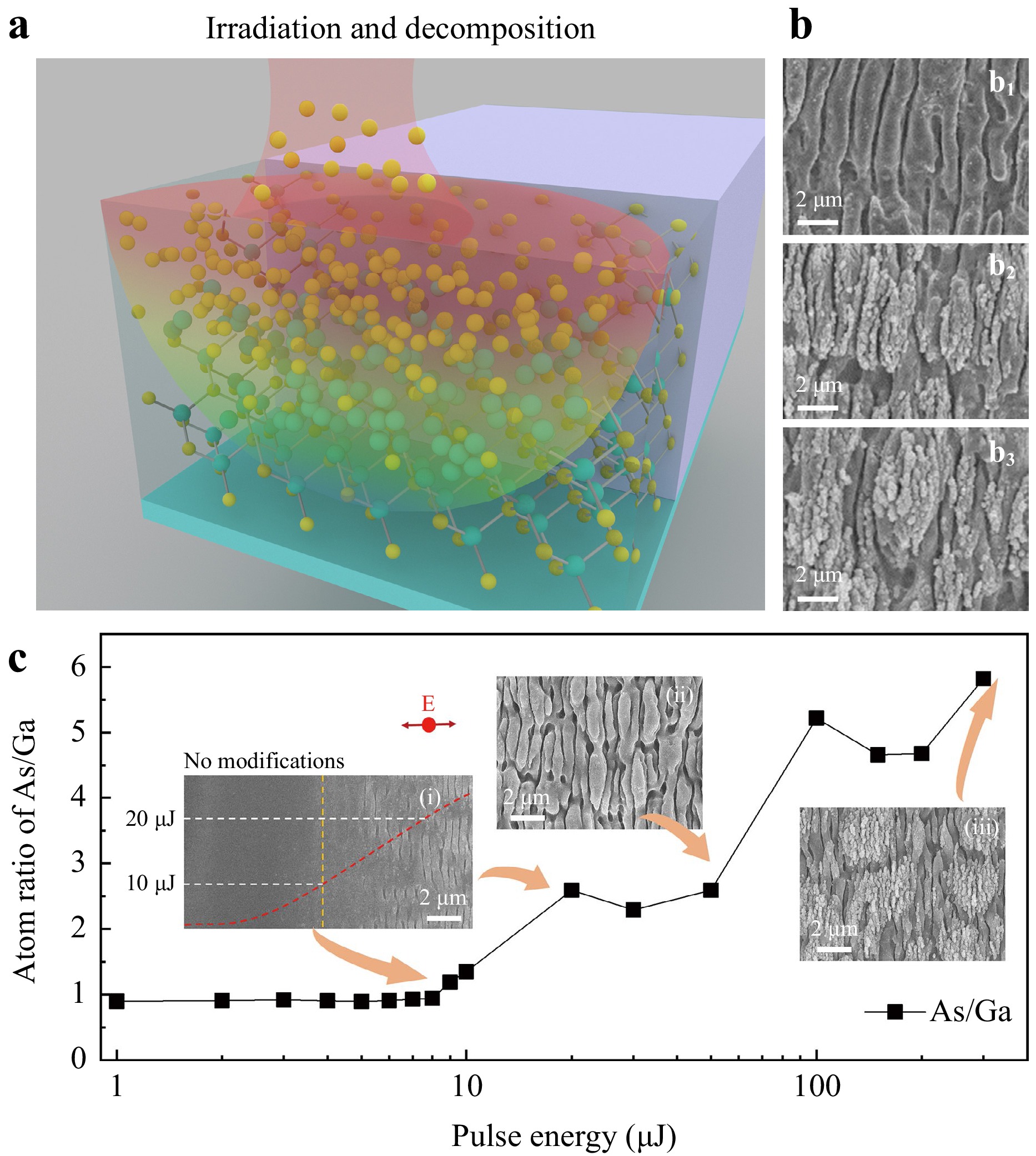 Published , Published online: 29 June 2024 , doi: 10.37188/lam.2024.026
The manipulation of micro/nanostructures to customise their inherent material characteristics has garnered considerable attention. In this study, we present the selective activation of gallium arsenide (GaAs) via ultrafast laser-induced decomposition, which correlates with the emergence of ripples on the surface. This instigated a pronounced enrichment in the arsenic (As) concentration around the surface while inducing a depletion of gallium (Ga) at the structural depth. Theoretical simulations based on first principles exhibited a robust inclination towards the phase separation of GaAs, with the gasification of As–As pairs proving more facile than that of Ga–Ga pairs, particularly above the melting point of GaAs. As an illustrative application, a metal-semiconductor hybrid surface was confirmed, showing surface chemical bonding and surface-enhanced Raman scattering (SERS) through the reduction of silver ions on the laser-activated pattern. This laser-induced selective activation holds promise for broader applications, including the controlled growth of Pd and the development of Au/Ag alloy-based platforms, and thereby opens innovative avenues for advancements in semiconductors, solar cell technologies, precision sensing, and detection methodologies.
-
Article
X-photon 3D lithography by fs-oscillators: wavelength-independent and photoinitiator-free
 Published , Published online: 31 December 2024 , doi: 10.37188/lam.2024.048
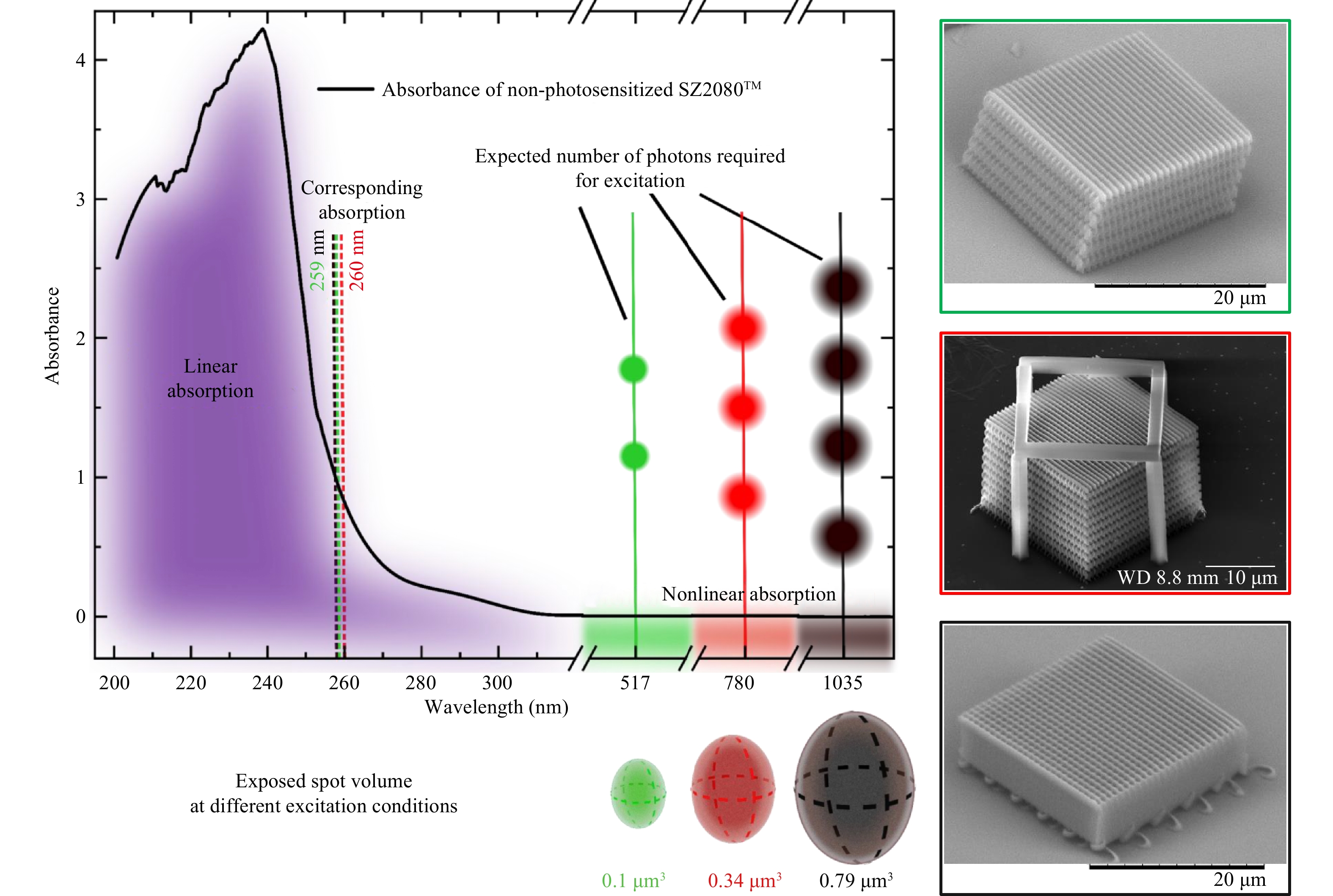
Laser direct writing employing multi-photon 3D polymerisation is a scientific and industrial tool used in various fields such as micro-optics, medicine, metamaterials, programmable materials, etc., due to the fusion of high-throughput and fine features down to hundreds of nm. Some limitations of technology applicability emerge from photo-resin properties, however any material modifications can strongly affect its printability, as photoexcitation conditions alter as well. Here we present wavelength-independent 3D polymerisation using low peak power laser oscillators. High pulse repetition rate and fast laser direct writing was employed for advancing additive manufacturing out of the SZ2080TM photo-resist without any photo-initiator. Wavelengths of 517 nm, 780 nm, and 1035 nm are shown to be suitable for producing 300 nm polymerized features even at high – up to 105 µm/s– writing speeds. Variation of organic-inorganic ratio in hybrid material results in shift and decrease of the dynamic fabrication window, yet not prohibiting the photo-structuring. Controlled energy deposition per focal volume is achieved due to localized heating enabling efficient 3D printing. Such spatio-selective photo-chemical cross-linking widens optical manufacturing capacity of non-photo-sensitive materials.
-
Article
Efficient synthesis of vitamin D3 in a 3D ultraviolet photochemical microreactor fabricated using an ultrafast laser
 Published , Published online: 16 March 2024 , doi: 10.37188/lam.2024.010
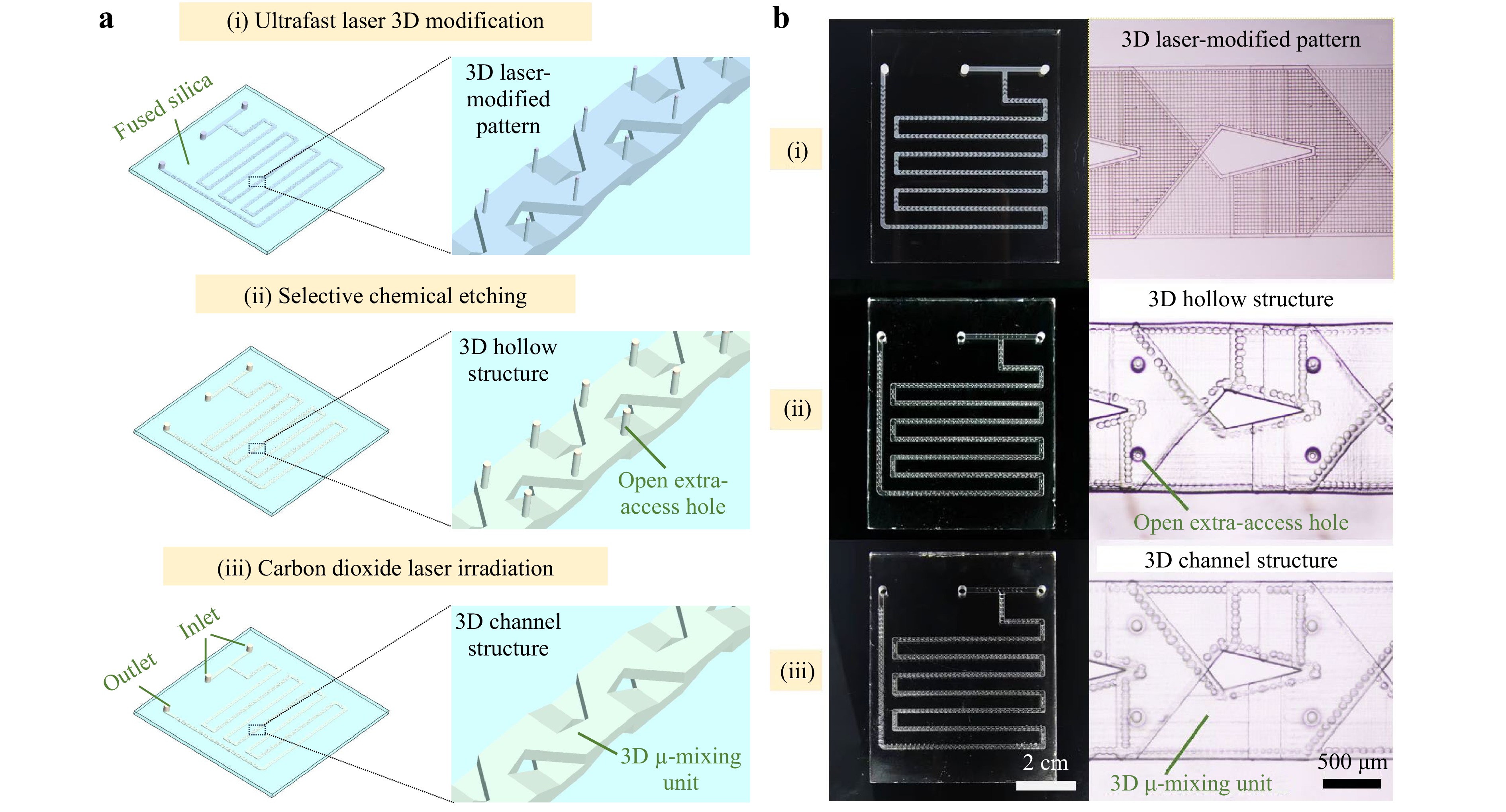
Large-scale, high-precision, and high-transparency microchannels hold great potential for developing high-performance continuous-flow photochemical reactions. We demonstrated ultrafast laser-enabled fabrication of three-dimensional microchannel reactors in ultraviolet (UV) grade fused silica which exhibit high transparency under the illumination of UV light sources of wavelengths well below 300 nm with excellent mixing efficiency. With the fabricated glass microchannel reactors, we demonstrated continuous-flow photochemical synthesis of vitamin D3 with UV LED array light sources.

Dong Wu is a professor of Engineering Science at the University of Science and Technology of China. He obtained Ph.D. degree from Jilin University in 2010 and then became a postdoc at RIKEN in Japan from 2011 to 2014. His thesis was awarded “100 Excellent Doctoral Theses” of China. His research interests are SLM-based high-efficiency femtosecond laser 3D micro-fabrication in various materials towards highly functional 2D-3D devices, which have found applications in nonlinear beam shaping, particles filtering, and cell manipulation. Prof. Wu has published 100 papers in the journals such as Nature Photonics, Nat. Comm., Light: Sci & Appl., PNAS, Laser Photon. Rev., Adv. Mater., ACS Nano and so on.

Liang Yang is a research professor at Suzhou institute for advanced research, University of Science and Technology of China (USTC). After completing his PhD in mechanical engineering (USTC) and Laser Zentrum Hannover in 2015, he spent two years as a postdoc at Micro/Nano Engineering Lab in USTC. From 2018-2022, he was a research scientist at Institute of Nanotechnology/Institute of Applied Physics at Karlsruhe Institute of Technology. His research interests comprise ultrafast optics, laser-matter interaction, laser micro/nano printing as well as 3D micro/nano devices for bio-medical engineering. This research has led to over 40 publications including Nat. Commun., Adv. Mater., Laser Photon. Rev., Light Adv. Manuf. etc.. He was selected into the 100-talent project of the Chinese Academy of Science.

Mangirdas Malinauskas defended Ph.D. in 2010 at Vilnius University, Laser Research Center - "Laser Fabrication of Functional 3D Polymeric Micro/Nanostructures", supervisor Prof. R. Gadonas. During career he has done traineeships at LZH (Prof. B.N. Chichkov) and IESL-FORTH (Dr. M. Farsari). In 2019-2022 a specially appointed Professor at Tokyo Institute of Technology (Japan), group of Prof. J. Morikawa. Currently he investigates fundamentals of laser 3D micro-/nano-structuring of cross-linkable materials for applications in micro-optics, nano-optics (photonics), and biomedicine at VU LRC. Laboratory funding is acquired via National, European, and worldwide (NATO, US Army) schemes. Optica Fellow in 2022.

Maria Farsari is a Research Director at FORTH/IESL (joined in 2003). She is one of the first to develop laser-based 3D micro/nano printing, a field she first got involved in as a postdoctoral researcher at Sussex University in 1997. She has pioneered the use of laser-made 3D scaffolds for cell growth and tissue engineering. Her research interests are light-enabled additive manufacturing, multiphoton lithography, with current focus on architected materials for biomedical applications.

Gordon Zyla has been working as a postdoctoral fellow in the Nonlinear Lithography group at IESL-FORTH, Crete, Greece, since 2021. He completed his mechanical engineering studies at Ruhr University Bochum (RUB), Germany. In 2020, he received his PhD in mechanical engineering from RUB. In 2021, he was awarded the Gateway Fellowship by the RUB Research School. Additionally, in 2022, he was named a Feodor Lynen Fellow by the Alexander von Humboldt Foundation. More recently, he was awarded a postdoctoral fellowship by the EU programme Marie Sklodowska-Curie Actions under Horizon Europe, and he served as a co-chair at the Photonics West conference in 2023.Dr. Zyla's research has primarily been focused on fabricating various micro- and nanoscale applications using 3D printing by two-photon polymerization. These applications include biomimetics, metamaterials, and micro-optics, among others. In his current Marie Sklodowska-Curie project, EagleEye, he aims to develop a novel printing approach enabling high-speed 3D printing with ultra-high resolution.

Patrick Salter is a Departmental Lecturer in Photonics at the Department of Engineering Science in the University of Oxford. Previously he held an Early Career EPSRC Fellowship and the Spooner Junior Research Fellowship at New College. His work centres on the application of adaptive optics to laser micro-fabrication, particularly the use of femtosecond pulse lasers to manufacture three dimensional devices inside transparent materials, applying adaptive optical techniques to enhance precision and/or speed. Areas of interest are devices inside diamond; liquid crystal photonics; and microscope calibration.

 Email
Email RSS
RSS