

View by Category
Published
, Published online: 10 October 2026
, doi: 10.37188/lam.2026.122
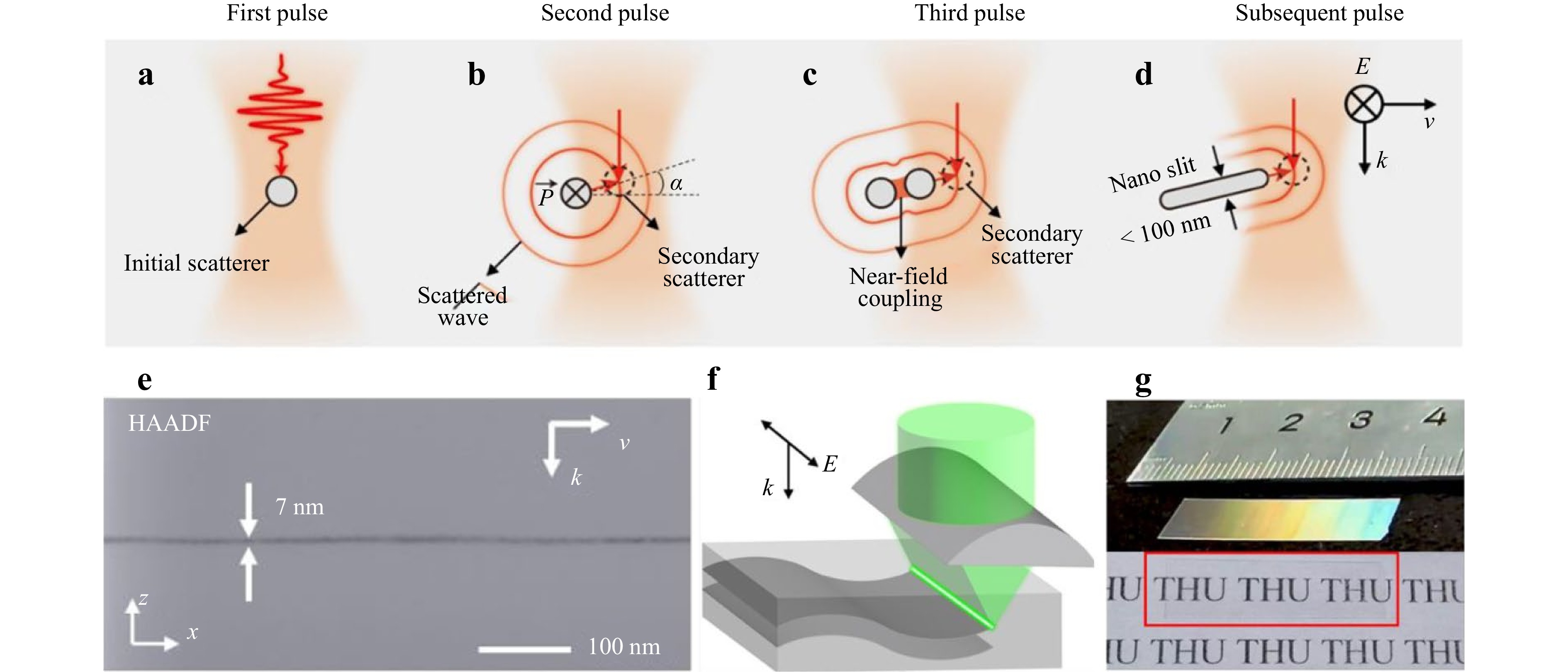
Chai et al. converted interferometric scattering from a persistent optical limitation into an effective tomoslicing technique, which delivers an unprecedented 7-nm kerf width and almost lossless wafering. Furthermore, this method is a robust and scalable approach for the low-waste manufacturing of transparent crystals and semiconductor substrates.


Published
, Published online: 10 October 2026
, doi: 10.37188/lam.2026.133
A recently reported tandem colloidal quantum dot photodiode architecture simultaneously addresses two long-standing challenges related to response speed and spectral selectivity in 1,550-nm light detection and ranging (LiDAR) application. By halving the effective junction capacitance through series-connected subcells and suppressing visible-light interference, this work demonstrates a promising route toward solution-processed 3D LiDAR sensing. In the future, combining this architectural concept with low-dielectric-constant material platforms and robust surface defect engineering could further reduce speed limitations while enhancing tolerance to ambient-light interference, potentially enabling picosecond-scale response in next-generation LiDAR systems.
Published
, Published online: 08 October 2026
, doi: 10.37188/lam.2026.123
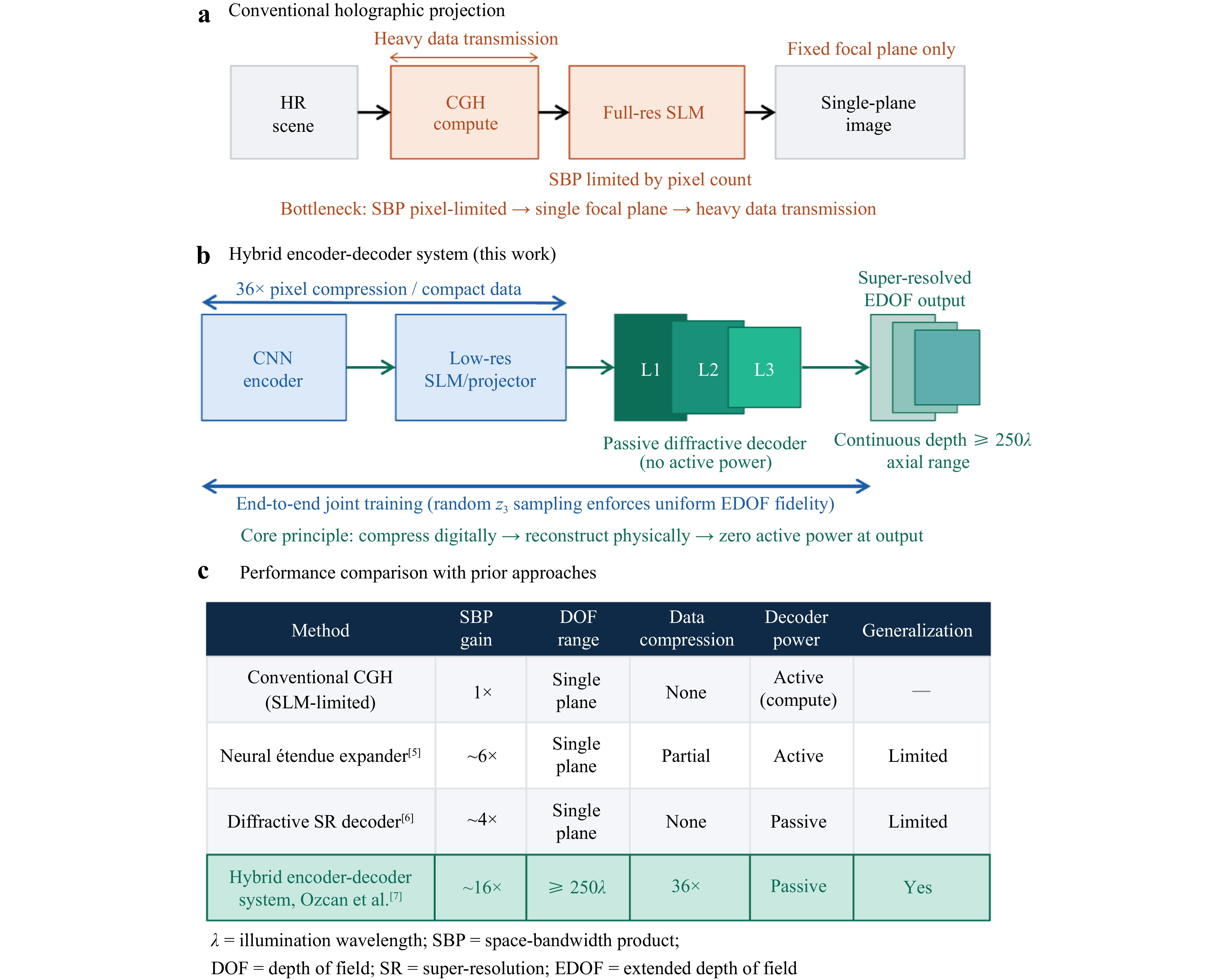
High-resolution holographic projection necessitates a high pixel count, wide depth of field, and compact data transmission—requirements that conventional spatial light modulators cannot simultaneously satisfy owing to inherent trade-offs. This challenge is mitigated by the proposed hybrid system that combines a neural-network digital encoder with a passive all-optical diffractive decoder. The convolutional neural network compresses inputs 36-fold into compact phase patterns, while a jointly trained stack of passive diffractive layers reconstructs them optically into super-resolved images across a continuous axial volume. This architecture achieved up to a approximately 16-fold space-bandwidth product improvement and a continuous depth of field of ≥ 250λ, with zero active power consumption at the output stage. It establishes a scalable framework toward realising energy-efficient, high-fidelity holographic projections for displays, metrology, and microscopy.

Published
, Published online: 20 July 2026
, doi: 10.37188/lam.2026.085
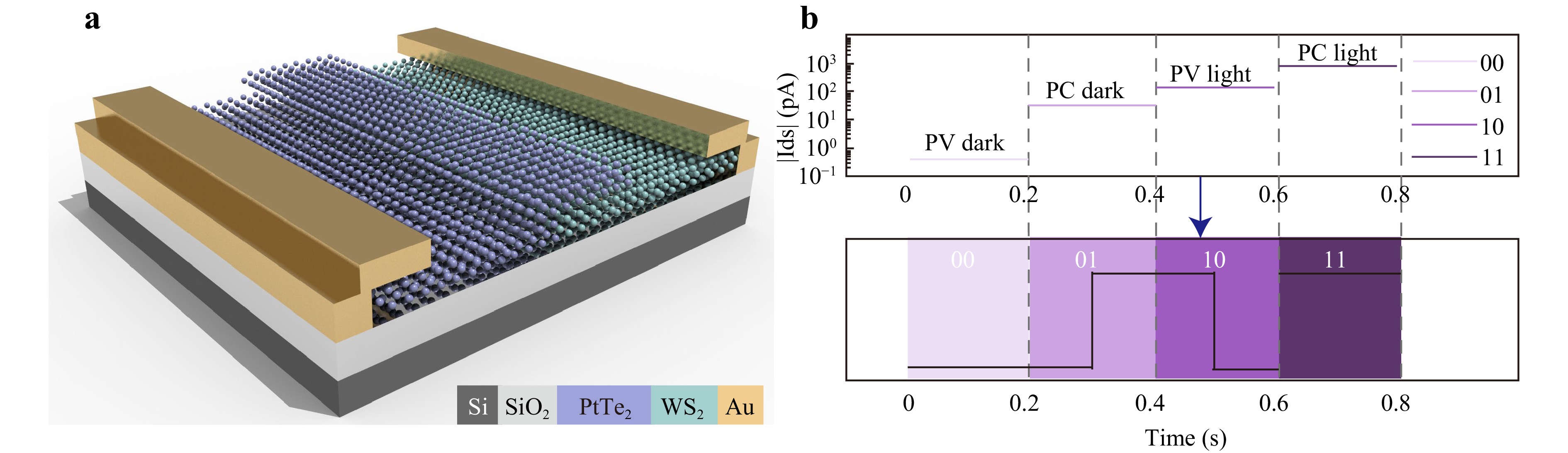
A bias-switchable van der Waals phototransistor demonstrates reconfigurable transitions between photovoltaic and photoconductive modes, generating four current states within a single device. This multi-state functionality advances on-chip optical logic and image encryption. It offers a promising route towards secure, low-power, and highly integrated photonic communication systems.
Published
, Published online: 17 August 2026
, doi: 10.37188/lam.2026.119
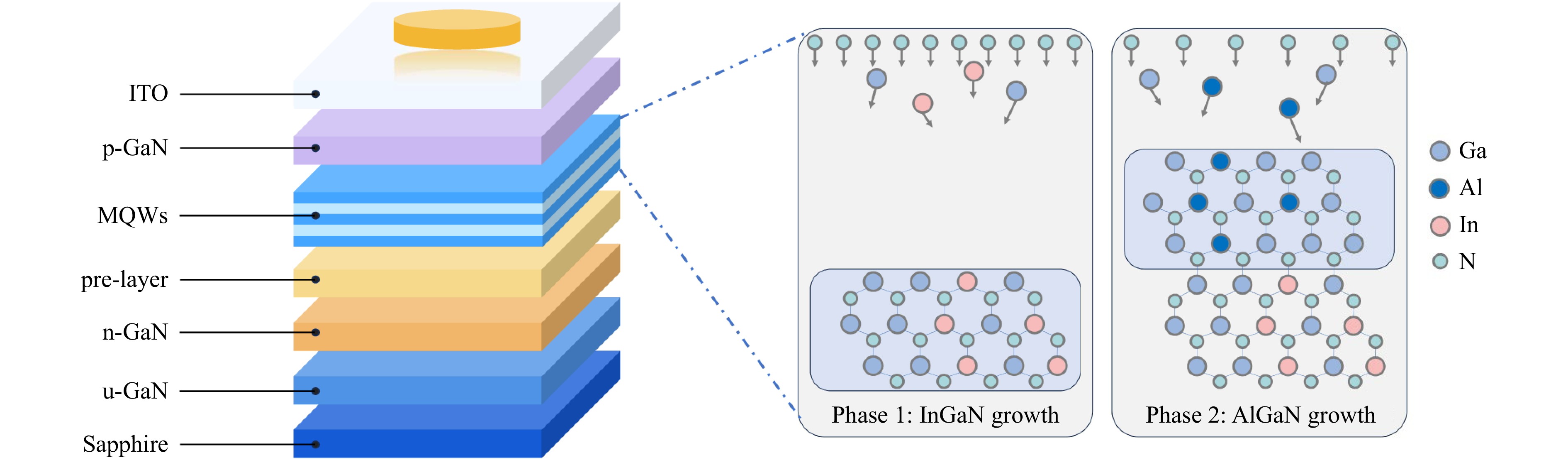
InGaN/AlGaN digital-alloy barriers have enabled weak-polarisation-field III-nitride light-emitting diodes (LEDs) on industrially compatible polar c-plane substrates. By optimising ammonia-flow-modulated pulse growth, this strategy improves digital-alloy interface quality, reduces the polarisation electric field to 0.5 MV/cm, and delivers blue LEDs with a peak external quantum efficiency of 15%. The resulting lateral carrier confinement mitigates sidewall-related efficiency loss, thus offering a practical pathway towards high-performance micro-LEDs.
Published
, Published online: 23 September 2026
, doi: 10.37188/lam.2026.130
Existing three-dimensional fibre shape-sensing systems involve trade-offs among compactness, spatial sampling density, and interrogation complexity. Luo et al. addressed these challenges by spatially encoding orthogonal curvature components using axially misplaced eccentric scatterers in a standard single-mode fibre, enabling millimetre-scale, single-channel reconstruction and scalable integration into robotic and minimally invasive devices.
Published
, Published online: 11 September 2026
, doi: 10.37188/lam.2026.126
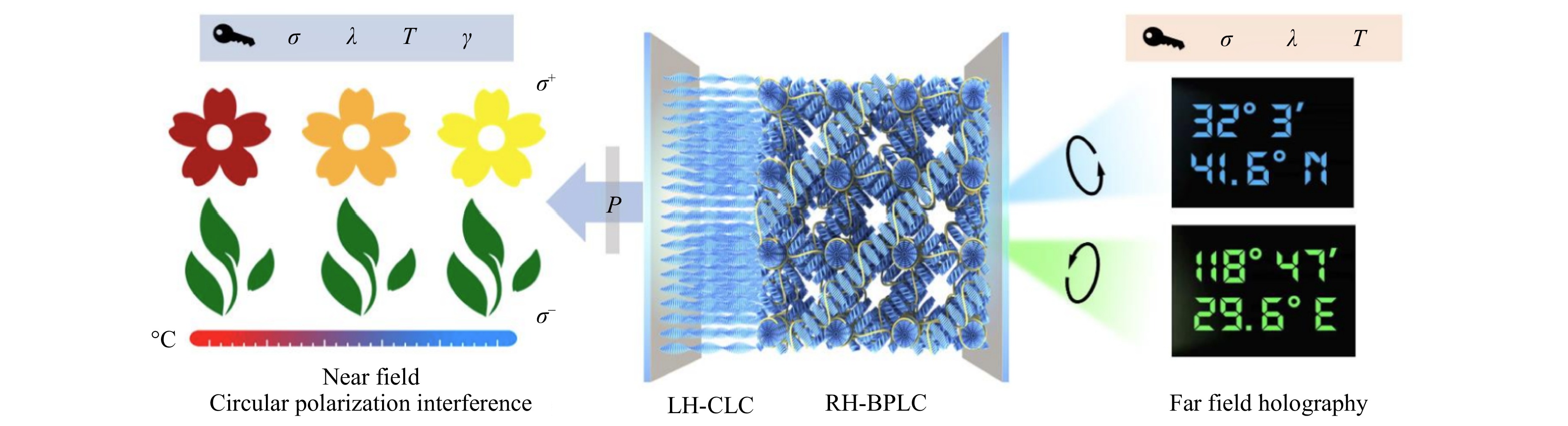
A biphasic chiral photonic crystal has been shown to support four structurally orthogonal encryption keys by exploiting physical and optical orthogonality. These results open new opportunities to engineer combinatorial key spaces in photonic platforms and for applications in optical security and anti-counterfeiting.

Published
, Published online: 27 April 2026
, doi: 10.37188/lam.2026.061
A recent study reported a suspended chalcogenide waveguide platform that enables ppb-level molecular gas sensing on a centimetre-scale photonic chip using near-infrared photothermal spectroscopy. These results highlight the use of suspended waveguides as a promising approach to achieving ultra-sensitive, fully integrated optical gas sensors by jointly engineering light–matter interaction and on-chip thermal management.
Published
, Published online: 10 June 2026
, doi: 10.37188/lam.2026.081
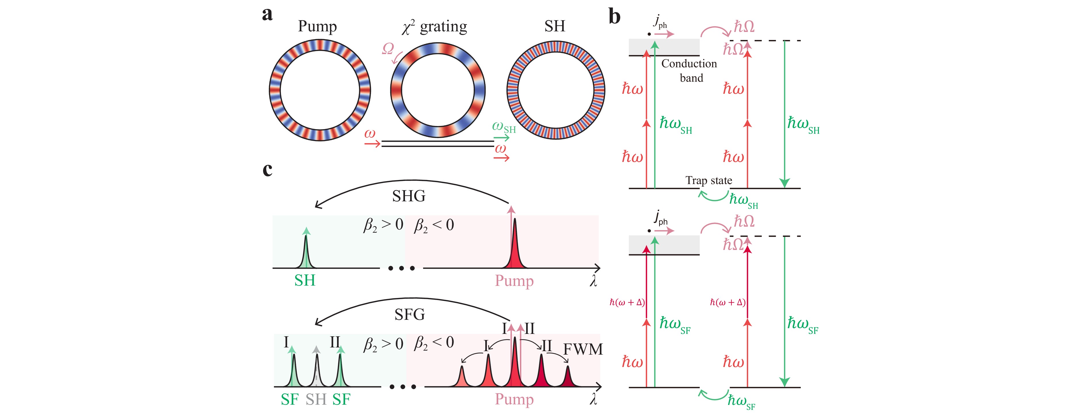
A widely tunable on-chip green light source in a silicon nitride (SiN) microresonator is demonstrated. By inscribing an effective \begin{document}$ \chi^{(2)} $\end{document} \begin{document}$ \chi^{(3)} $\end{document}
Published
, Published online: 10 June 2026
, doi: 10.37188/lam.2026.058
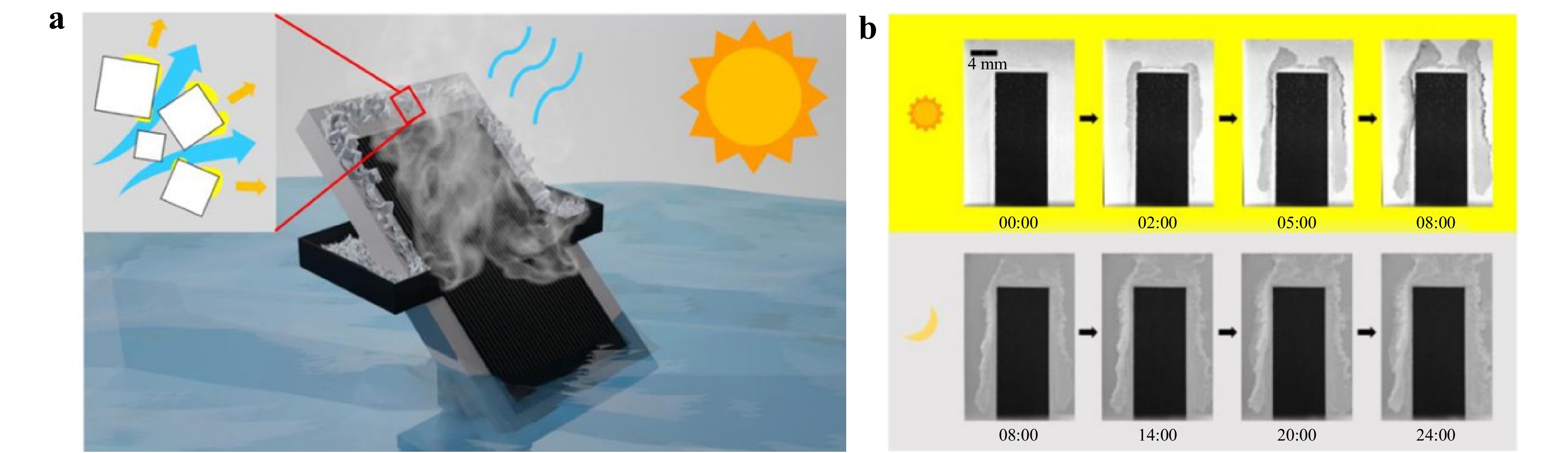
Solar-thermal interfacial evaporation provides an energy-efficient solution for decentralised desalination. However, its practical application with real seawater is hindered by salt accumulation and brine discharge. In a recent study, a laser-nanostructured, superwicking metallic interface that fundamentally decouples evaporation from crystallization was demonstrated. By using directional capillary transport to direct mineral growth away from the photothermal active zone, this platform enables stable, high-flux desalination of raw ocean water while allowing for nearly complete salt harvesting. This work marks a pivotal shift toward zero-liquid-discharge systems, redefining seawater as both a water source and harvestable reservoir for the circular mineral economy.
- First
- Prev
- 1
- 2
- 3
- 4
- 5
- Next
- Last
- Total:5
- To
- Go

 Email
Email RSS
RSS