
View by Category
Published
, Published online: 03 June 2026
, doi: 10.37188/lam.2026.074
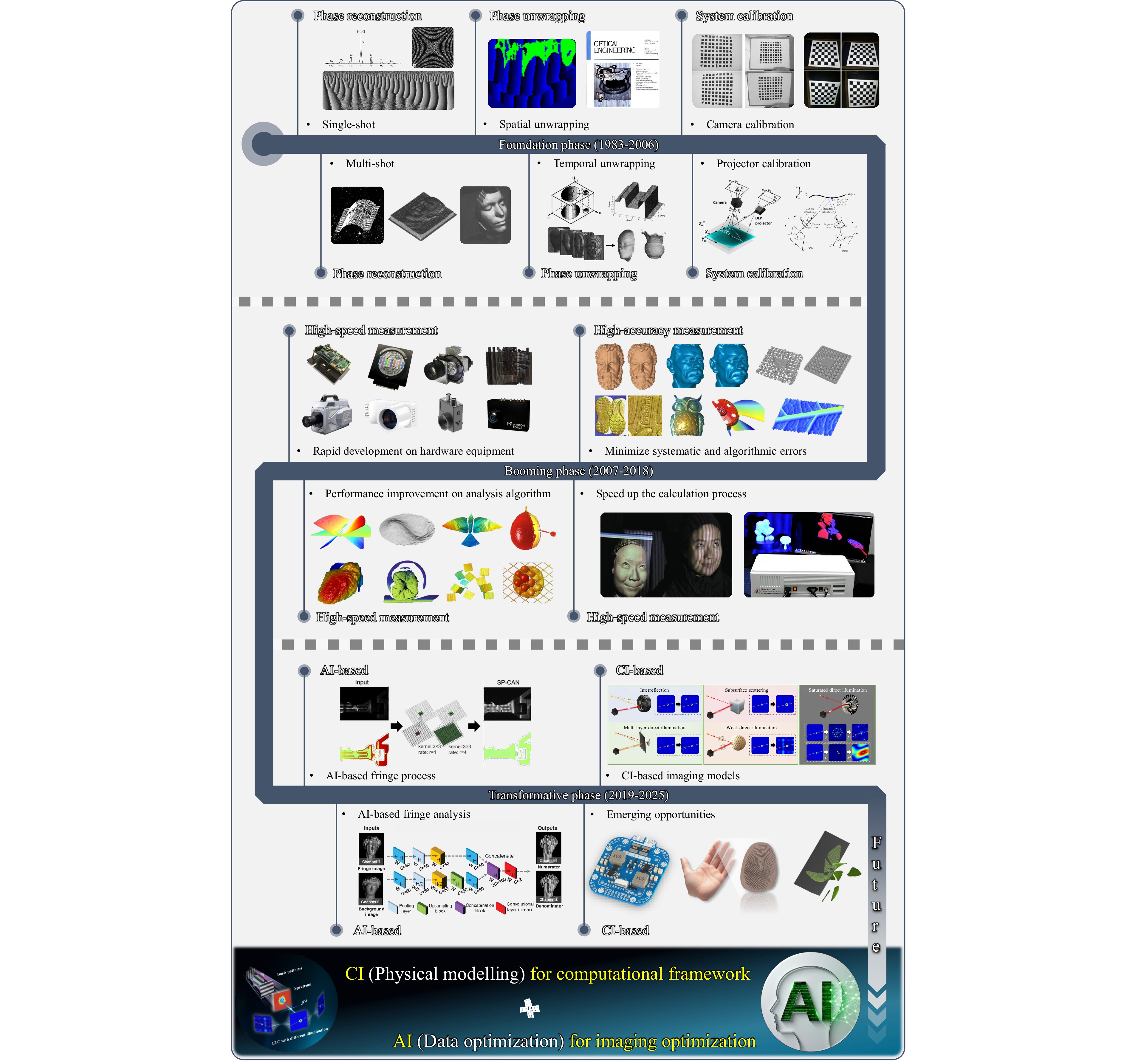
With the rapid advances in digital technologies and intelligent manufacturing, three-dimensional (3D) imaging based on fringe projection has laid the foundation for machine vision, industrial metrology, and interdisciplinary applications. This review provides a comprehensive overview of fringe projection profilometry (FPP), which is a widely adopted technology in the 3D imaging landscape. First, we outline the fundamental principles, implementation procedures, and historical developments of FPP. Next, we present the continuous advances in algorithms, hardware, and applications that collectively push FPP towards increasingly challenging measurement scenarios. Subsequently, we provide a dedicated discussion to explain the transformative roles of artificial intelligence (AI) and computational imaging (CI), delineating how their progress is initiating a shift from traditional geometric approaches towards computational 3D imaging. The current challenges and emerging trends in 3D imaging are further identified and discussed. Looking ahead, FPP is expected to evolve into a next-generation 3D imaging technique, achieving unprecedented accuracy, efficiency, and adaptability through the co-optimization of systems with algorithms and the convergence of AI and CI, thereby empowering more complex requirements across industrial, biomedical, and scientific domains.


Published
, Published online: 06 May 2026
, doi: 10.37188/lam.2026.021
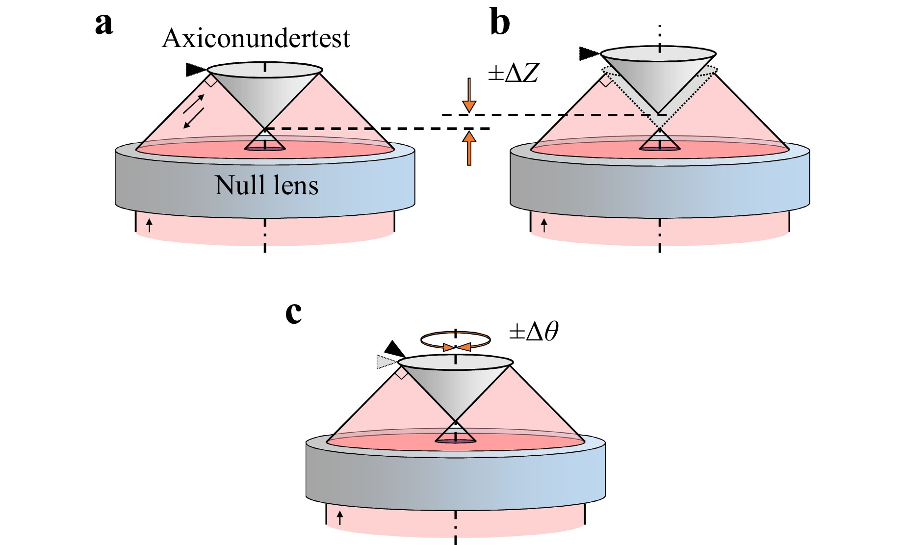
Metrology is a prerequisite for all advanced fabrication methods. For precision optical systems, optical surfaces require form accuracies down to nanometer level-accross areas with lateral dimensions measuring centimeters to decimeters, or even larger for astronomical instrumentation. This poses a challenge specifically for aspheric and freeform surfaces that scientists have tackled ever since the fabrication technologies allow the production of these, from an optics designer point of view, superior surfaces. In this work, we discuss several state-of-art metrology approaches with a focus on calibration. Specifically, we restrict ourselves to interferometric areal methods that have the potential to acquire a dense 2D surface deviation map within a short data acquisition time of less than a minute.


Published
, Published online: 23 March 2026
, doi: 10.37188/lam.2026.035
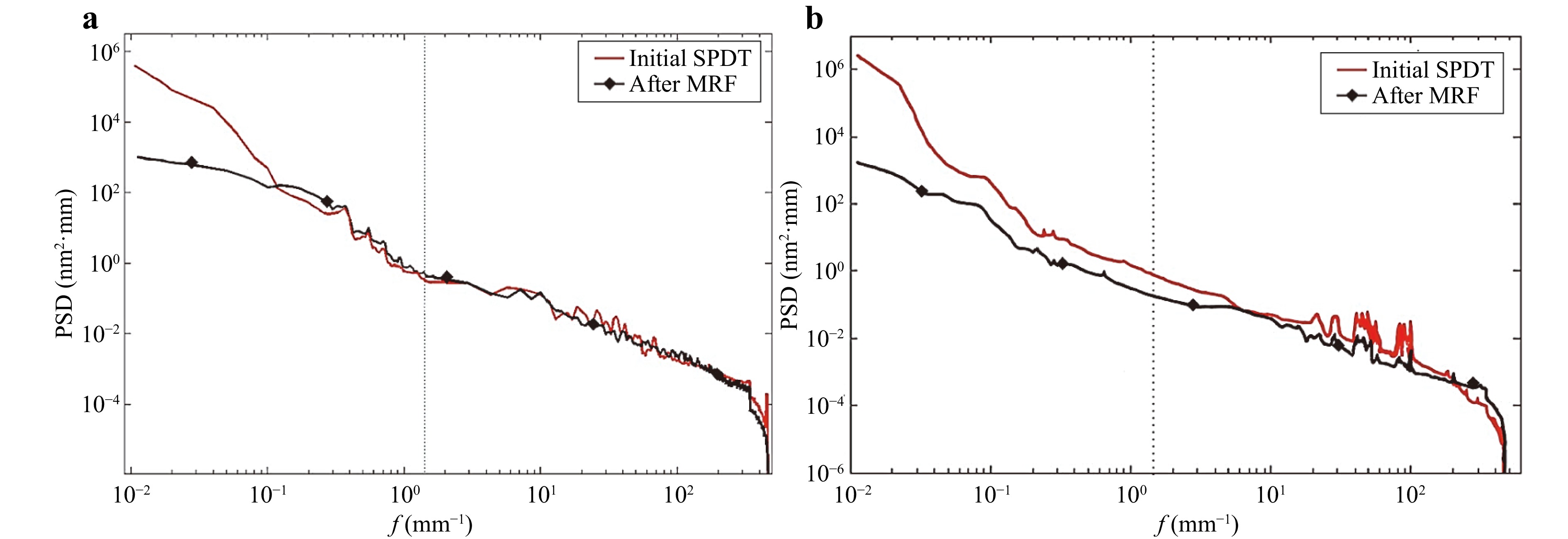
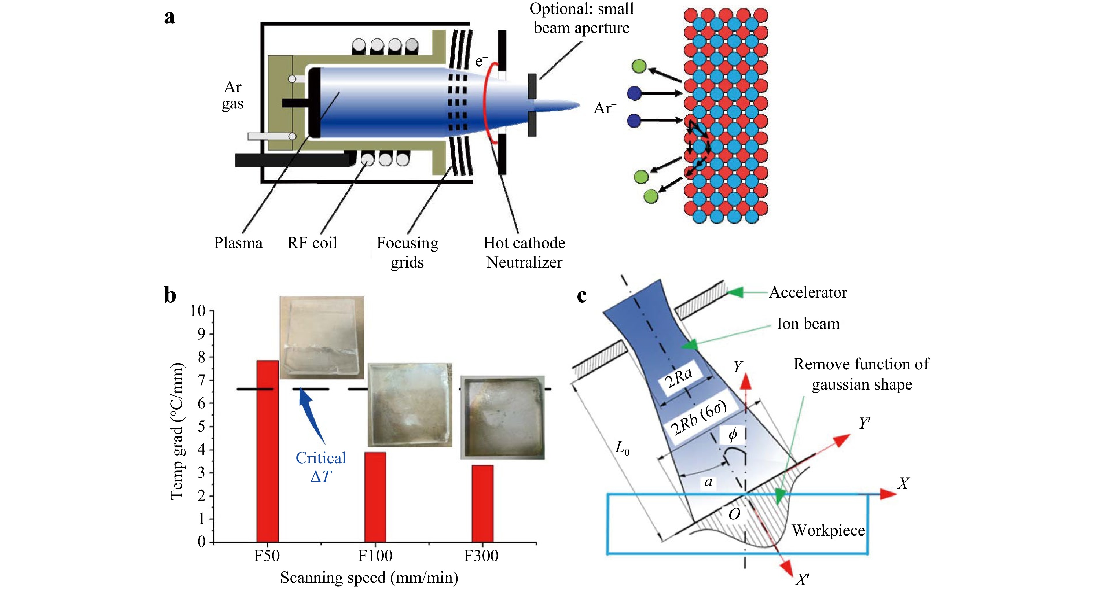
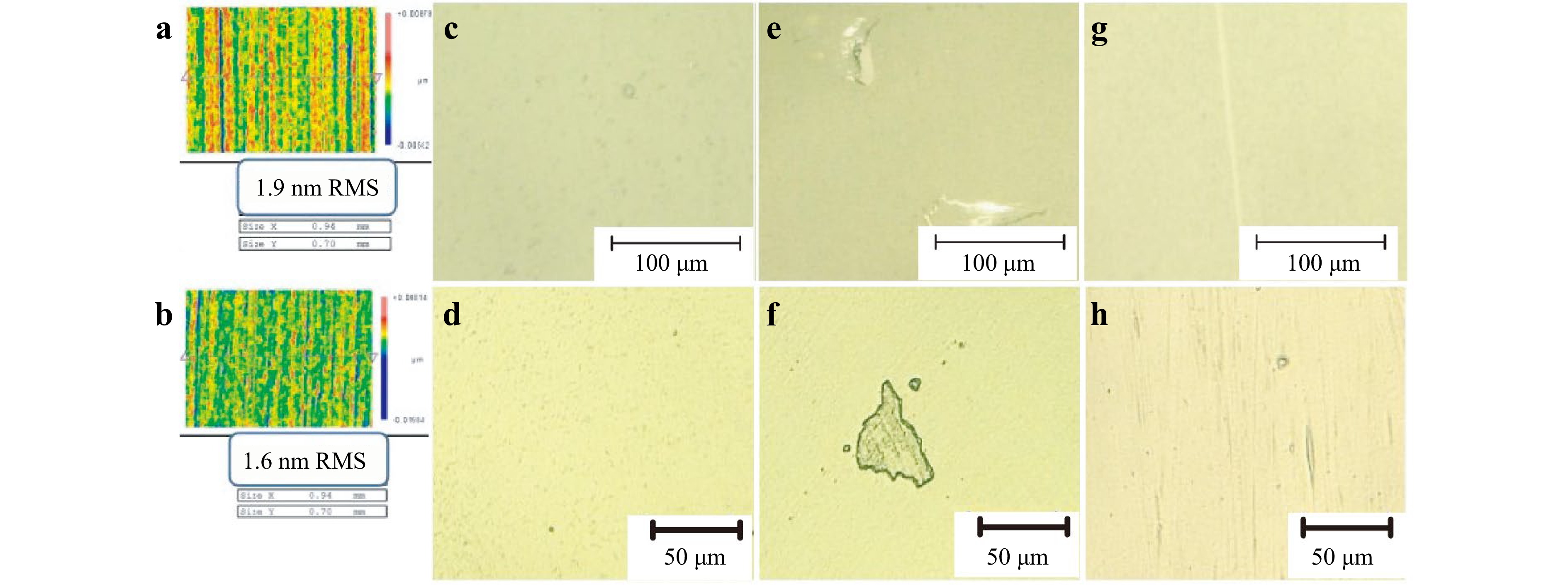
The relentless pursuit of higher resolution and sensitivity in astronomical observation drives the advancement of telescope mirror manufacturing. This review systematically charts the technological evolution from material innovation to the deterministic control of full-spatial-frequency errors. We analyze the progression of substrate materials—including silicon carbide, beryllium alloys, and advanced glass-ceramics—focusing on their critical thermomechanical properties for extreme environments. The core manufacturing chain is thoroughly examined: ultra-precision diamond turning for initial form generation, grinding processes exploiting brittle-to-ductile transitions, and advanced polishing techniques like magnetorheological finishing and ion beam figuring that achieve nanometer-level accuracy. A central theme is the paradigm shift towards segmented mirrors, which necessitates solving system-level challenges in edge control, co-phasing, and high-consistency batch production. The integration of field-assisted machining and intelligent systems, such as digital twins and robotics, is highlighted as a key enabler for next-generation manufacturing. While significant progress is evident, core challenges persist in stable sub-nanometer finishing, subsurface damage mitigation, and long-term performance under operational extremes. Future development hinges on deeper material-process co-design, fully integrated metrology-manufacturing loops, and sustainable production frameworks. This synthesis provides a comprehensive technical foundation for developing the extreme optical systems required for future discoveries in astrophysics.


Published
, Published online: 19 March 2026
, doi: 10.37188/lam.2026.001
Precision aspherical lenses are in high demand for a wide range of industrial and consumer products. While plastic lenses have gained popularity for low cost and flexibility, glass remains the superior material for high-end optics for its exceptional optical properties. Glass molding is a modern manufacturing technique that offers both high precision and affordability. This review, aimed at both academic and industrial communities, provides a brief history of this technology followed by a detailed discussion of the fundamental physics and modeling involved in the molding process. The review also includes a brief discussion of optical design and forming equipment but focuses on the molding process. In addition to conventional methods, we also cover special molding techniques like rapid heating and wafer-level glass molding, as well as the molding of chalcogenide glass lenses. By examining key developments in material modeling, mold fabrication, heat transfer and process optimization, this review aims to support ongoing advancements for next-generation precision optical manufacturing processes.


Published
, Published online: 12 October 2025
, doi: 10.37188/lam.2025.055
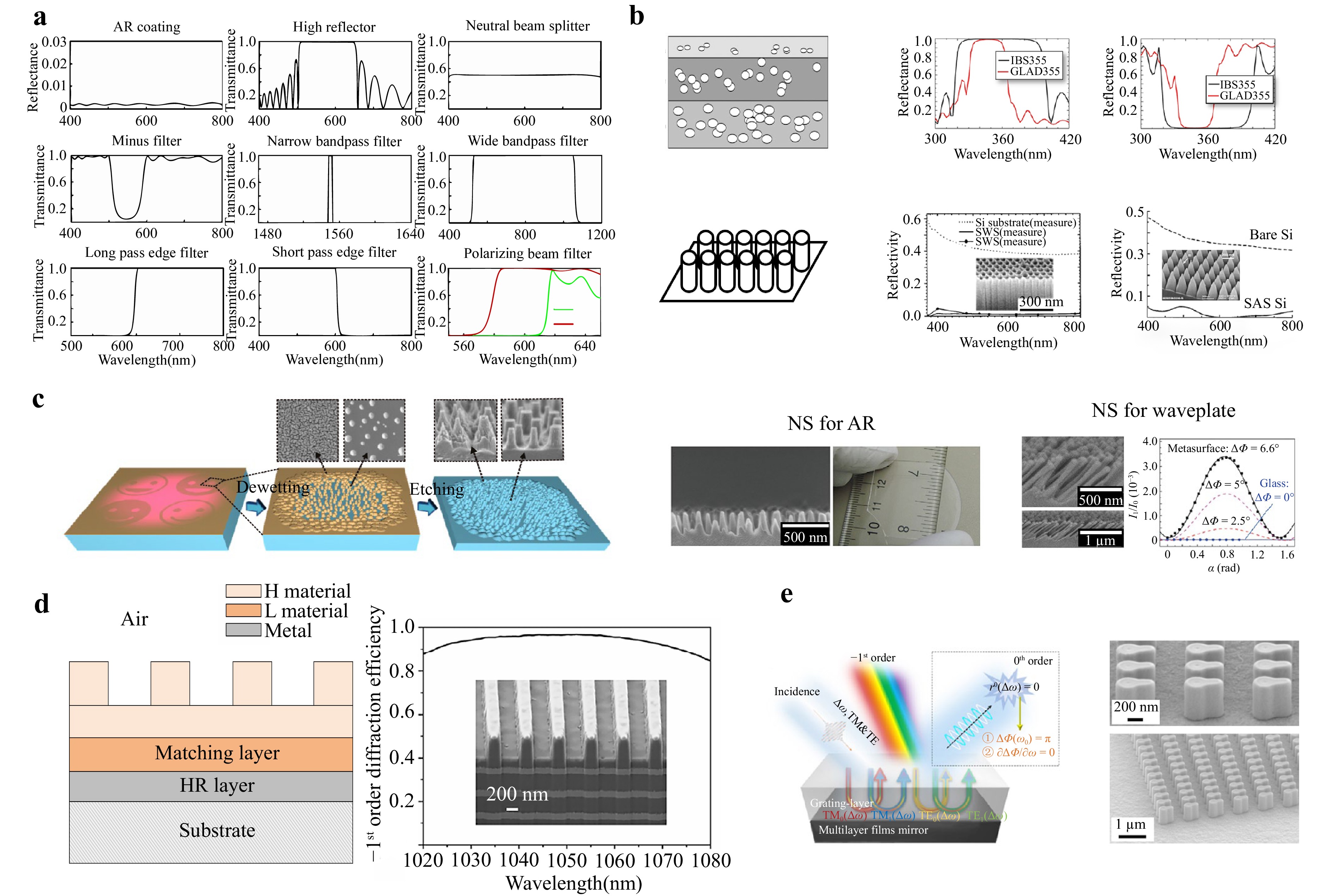
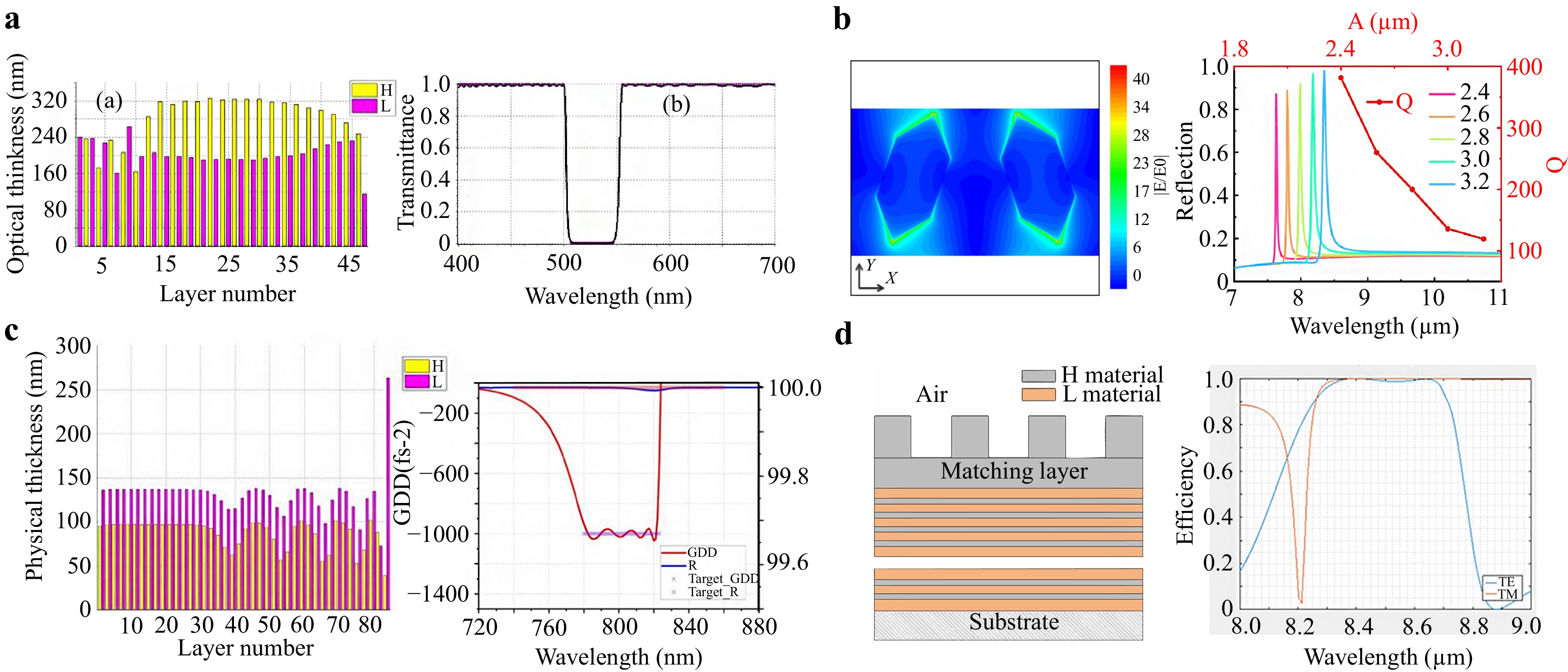
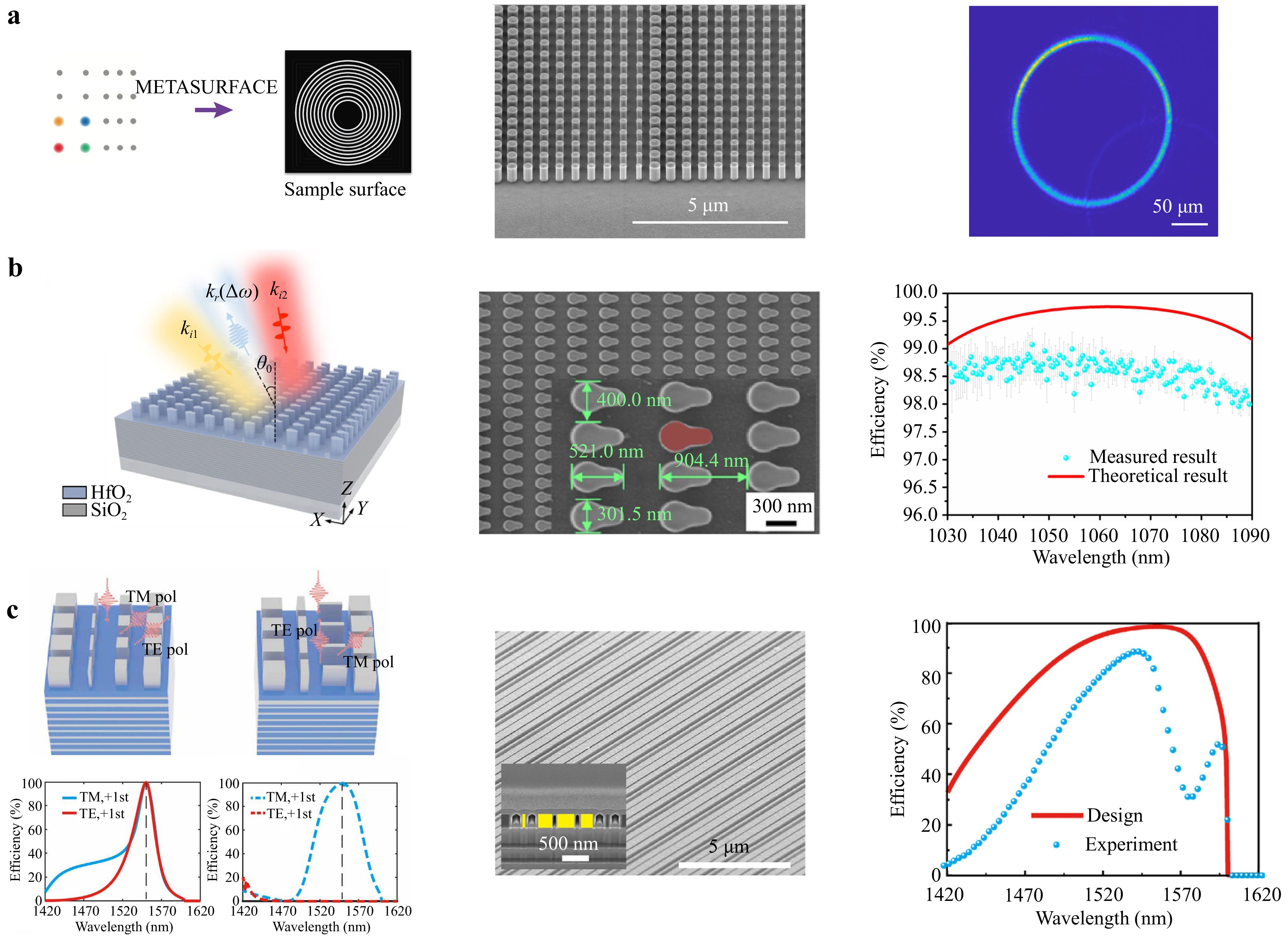
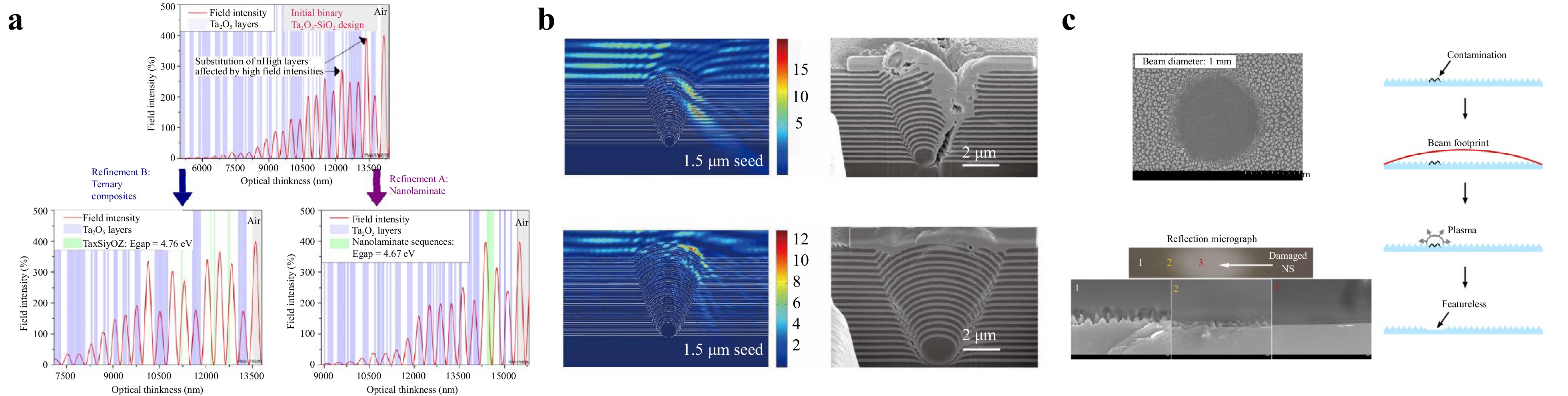
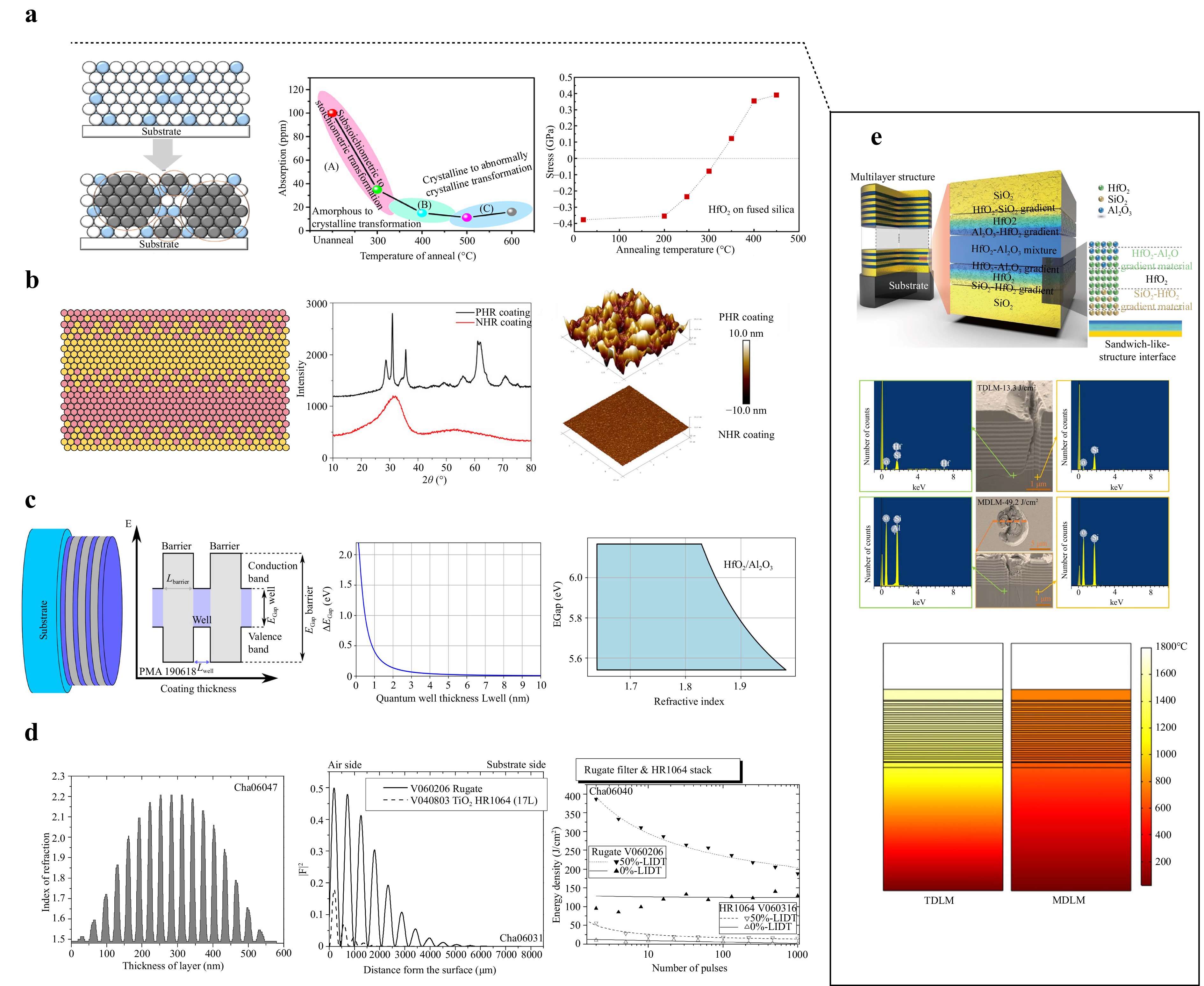
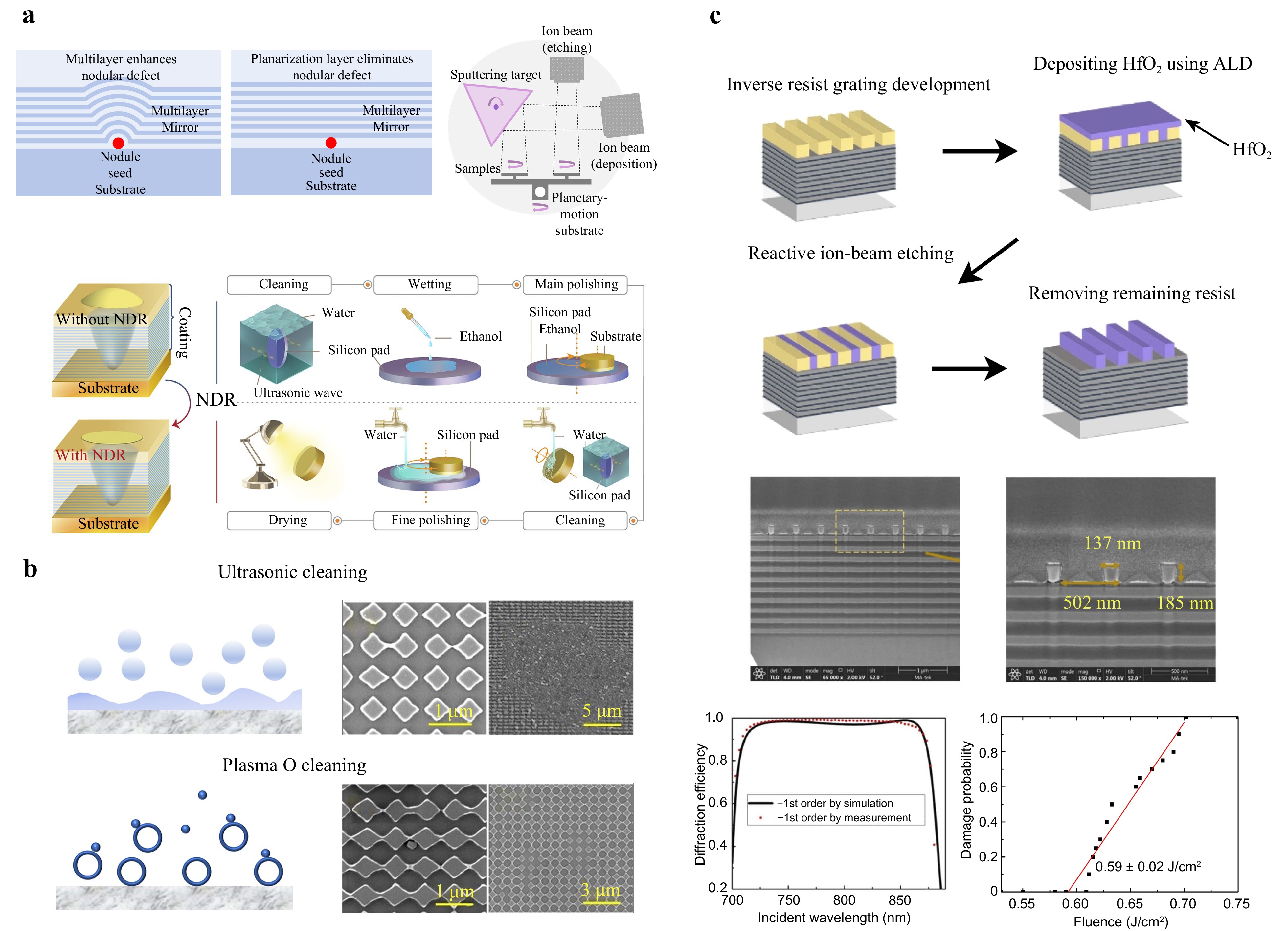
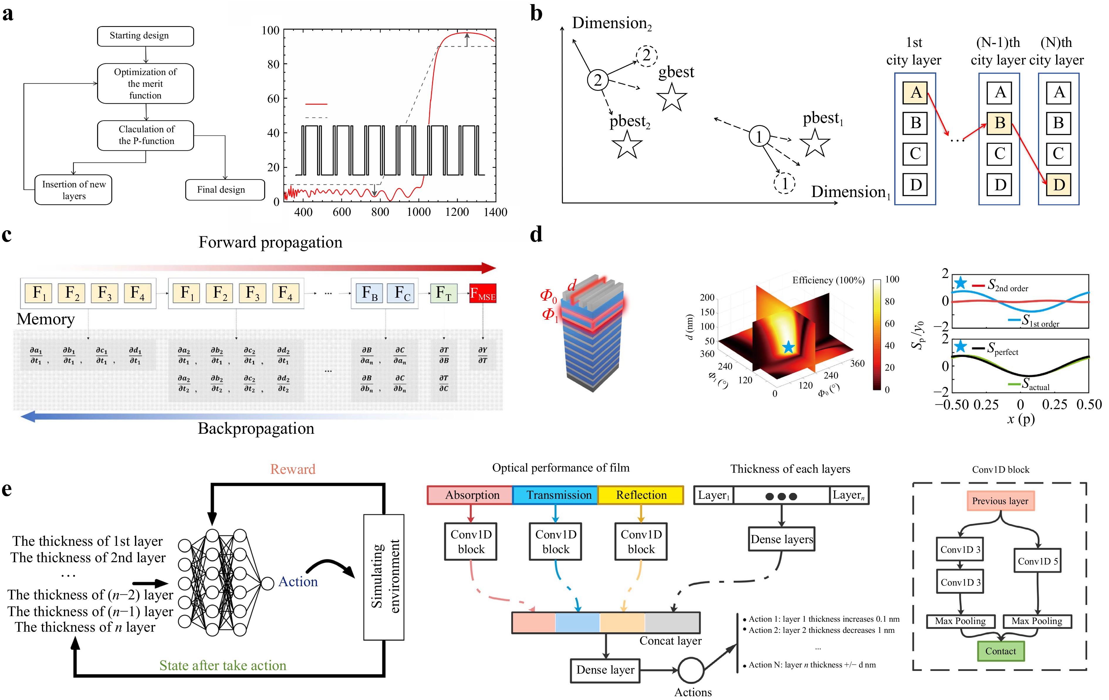
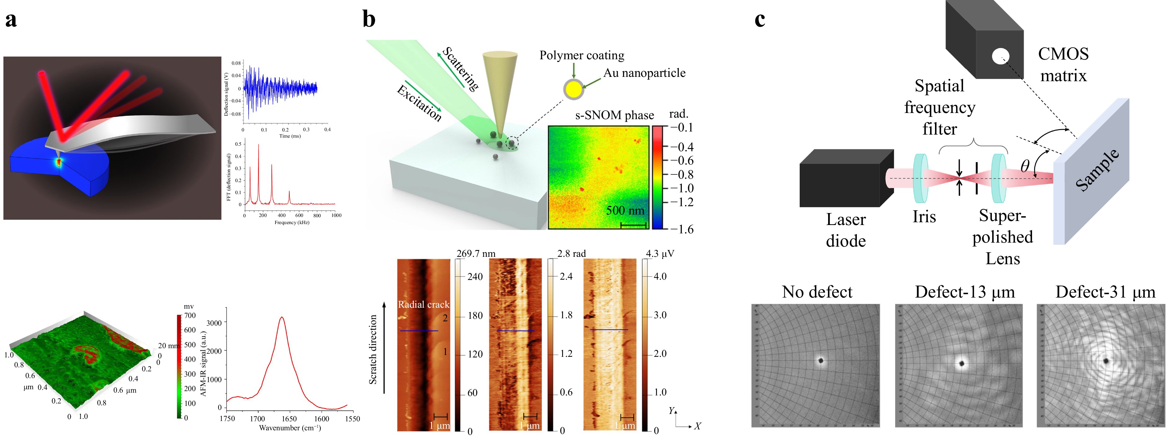
High-power laser coatings play a critical role in enabling optical manipulation in various laser applications, including beam alignment and control in high-power laser systems. These coatings rely on multilayers and microstructures, such as antireflective (AR) and highly reflective (HR) coatings, filters, and beam splitters, to enhance their performance. This review focuses on laser coatings used for manipulating optical fields, their principal limitations, and laser-induced damage in high-power applications. The concepts, principles, and progress made in exploring the optical performance and distinctive functions of the optical coatings and optimising the laser resistance through structural optimisation, material engineering, and defect elimination are highlighted. Finally, future directions for improving the design flexibility, fabrication feasibility, advanced detection techniques for high-resolution defect characterisation, and further consideration of minimising the optical loss are discussed to meet the evolving demands of modern high-power laser systems.
Published
, Published online: 03 September 2025
, doi: 10.37188/lam.2025.059
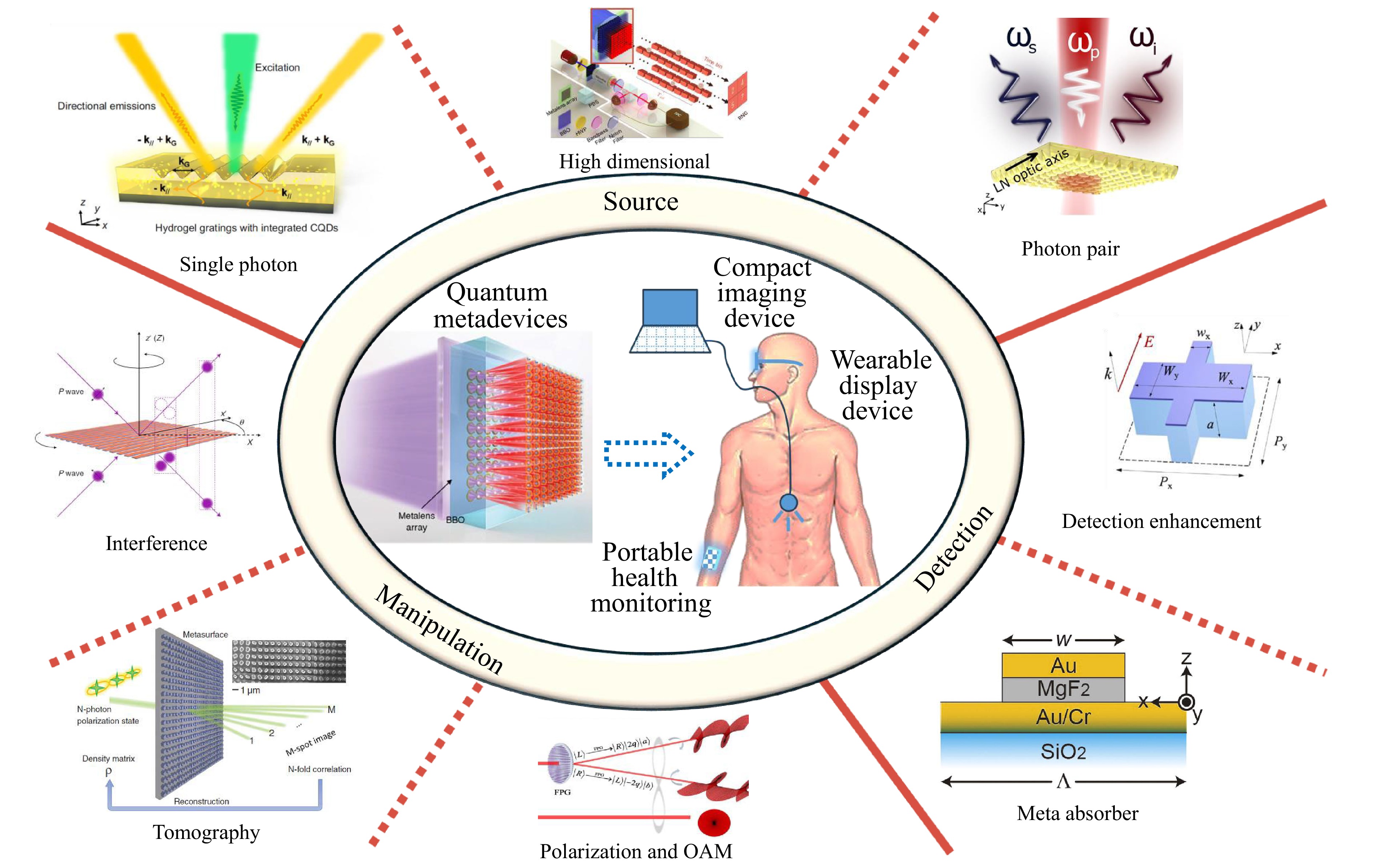
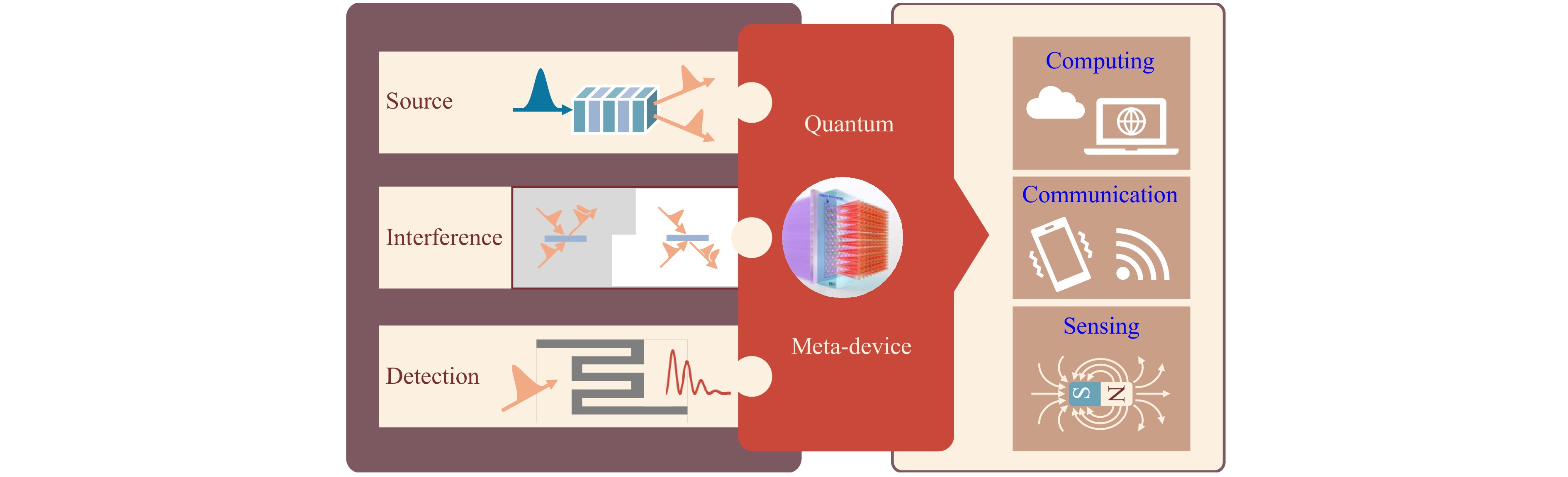
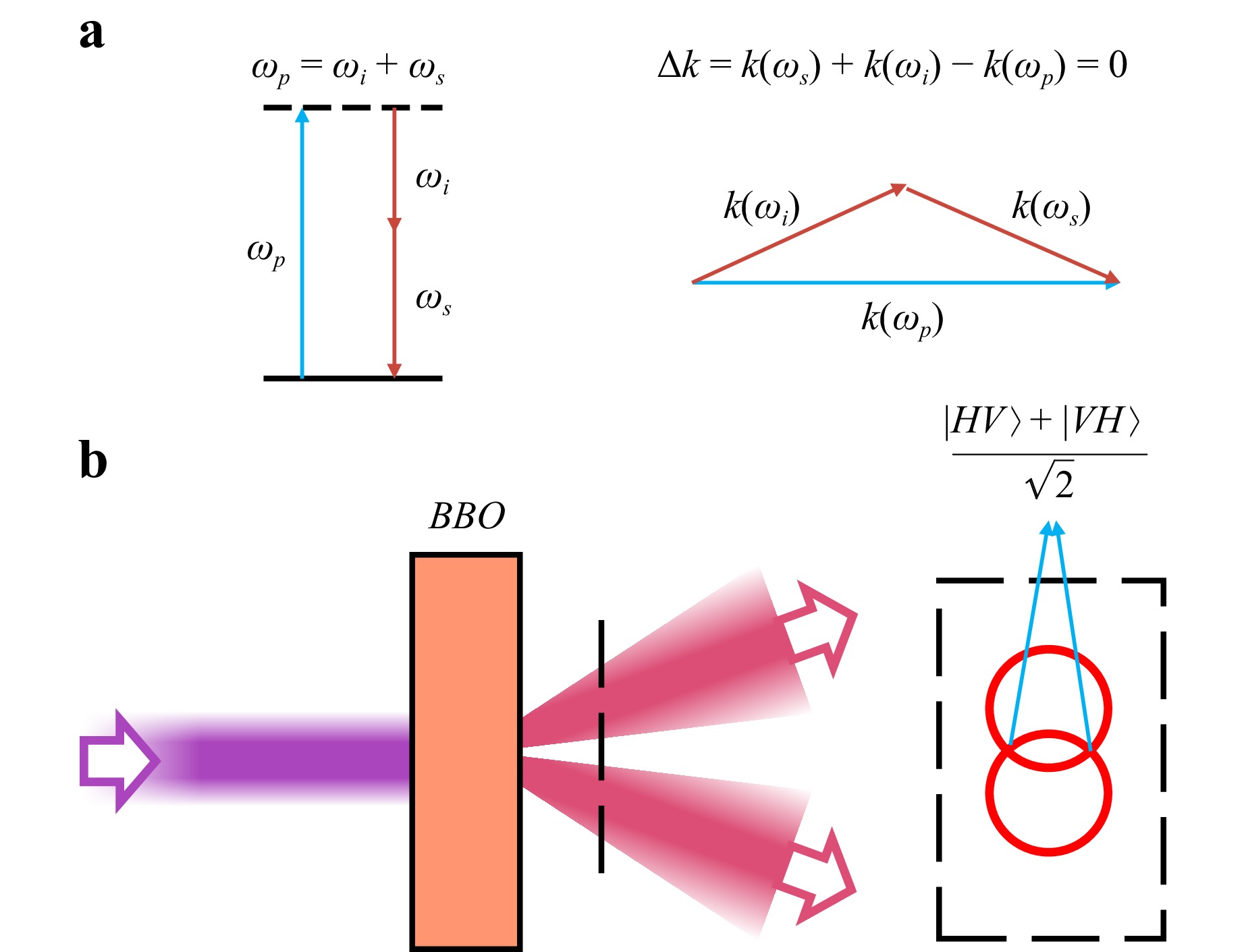
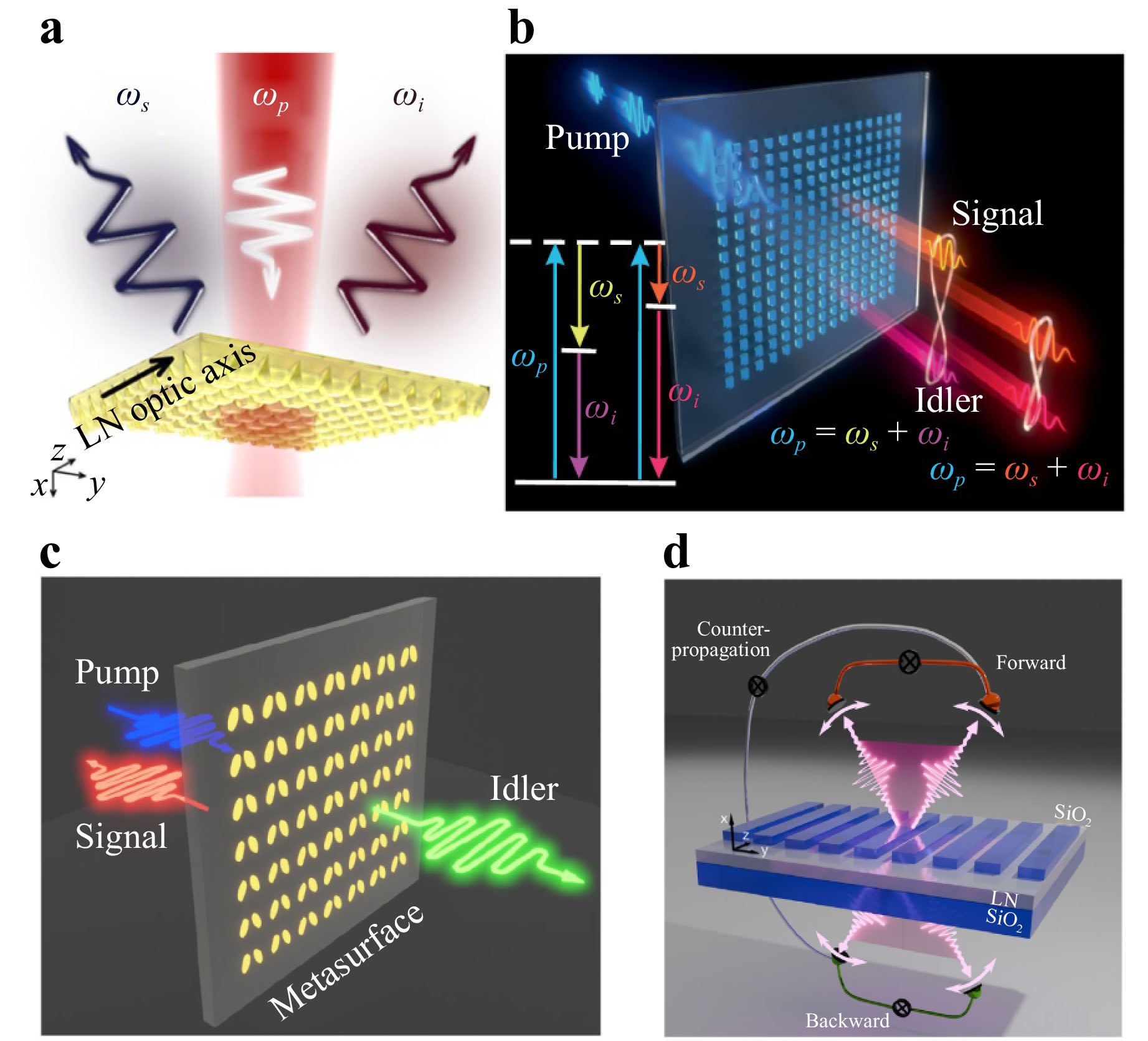
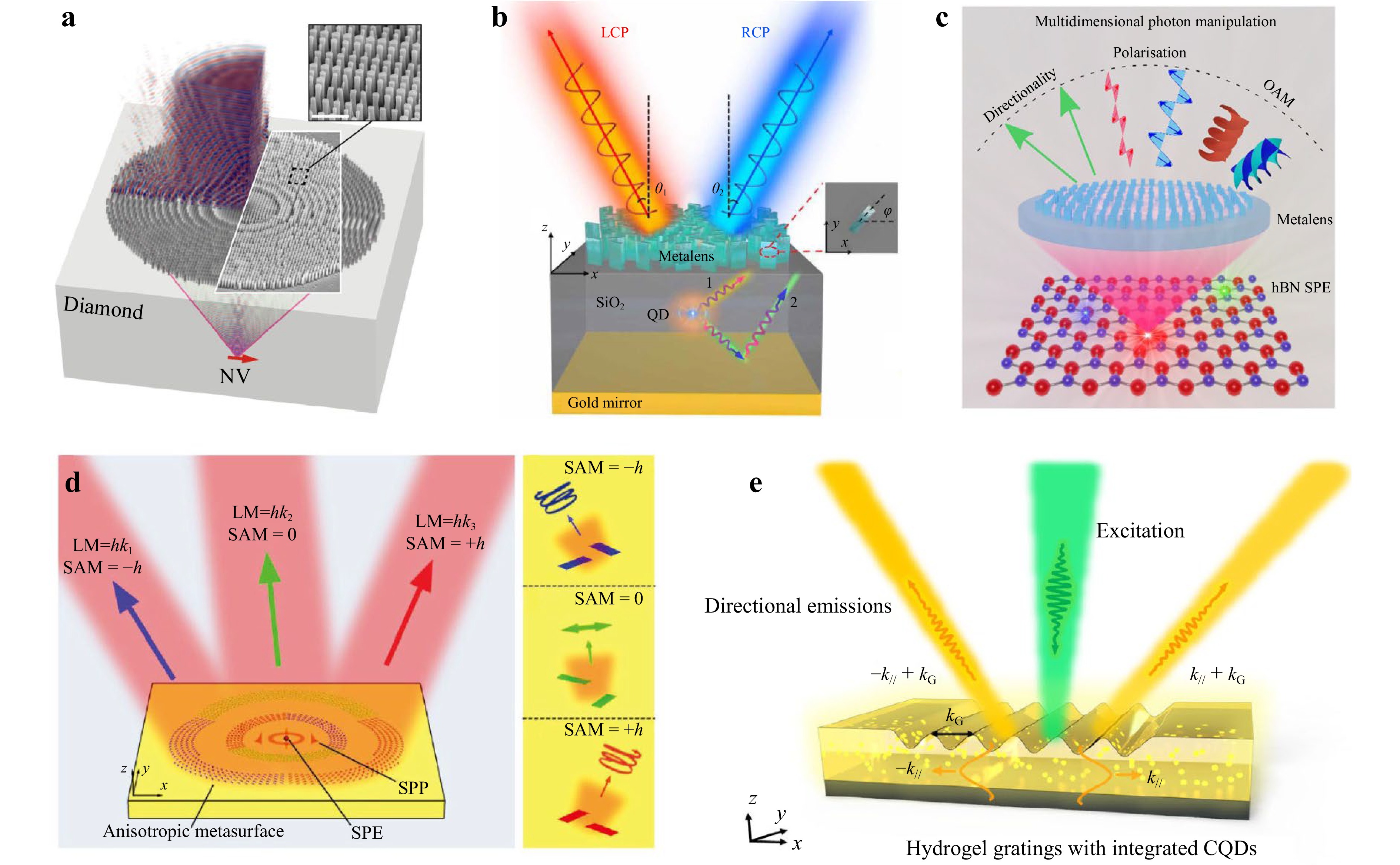
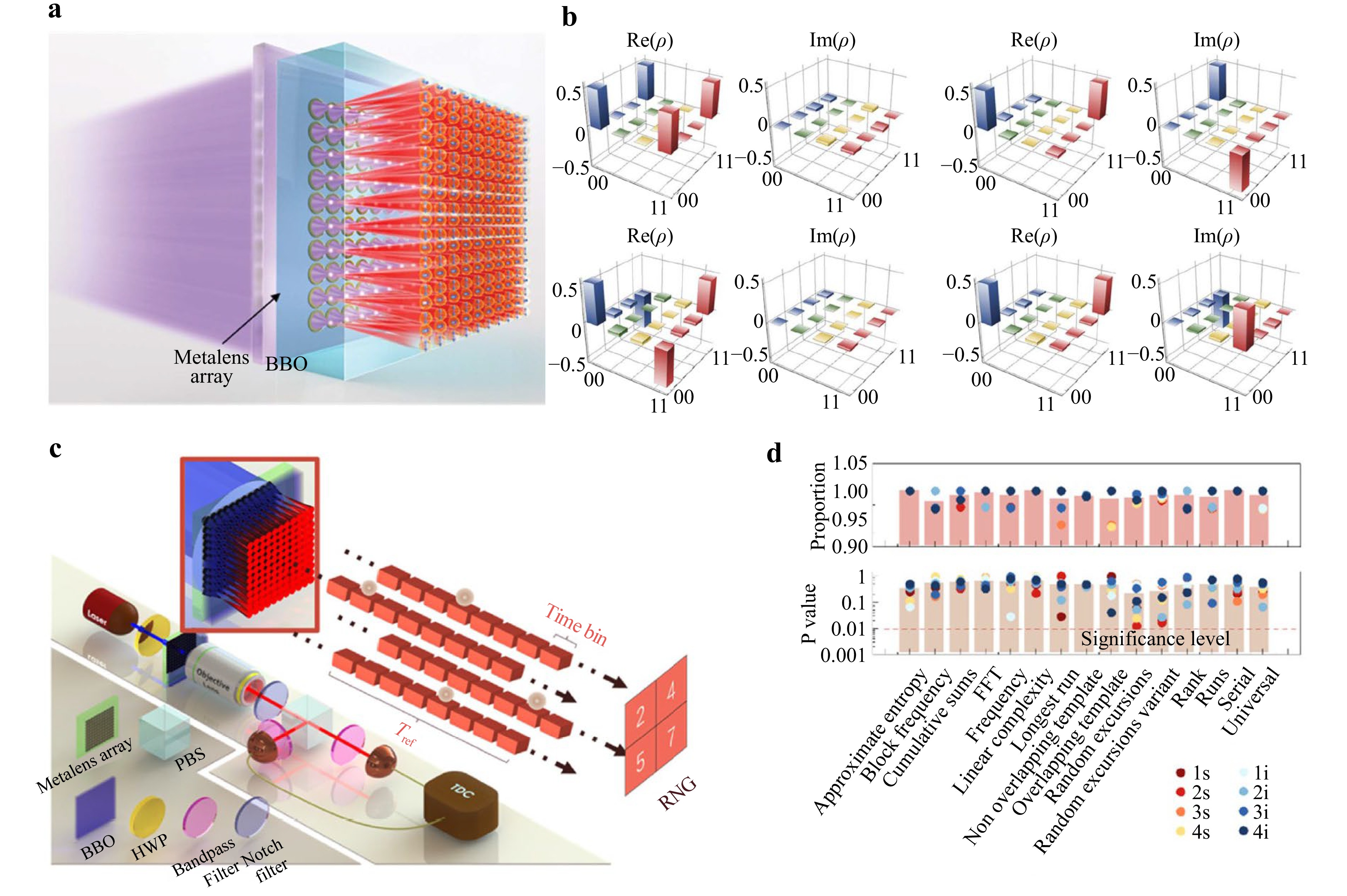
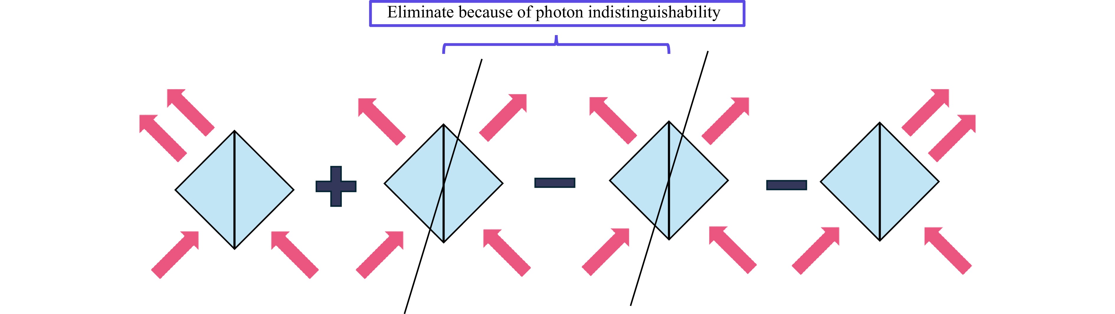
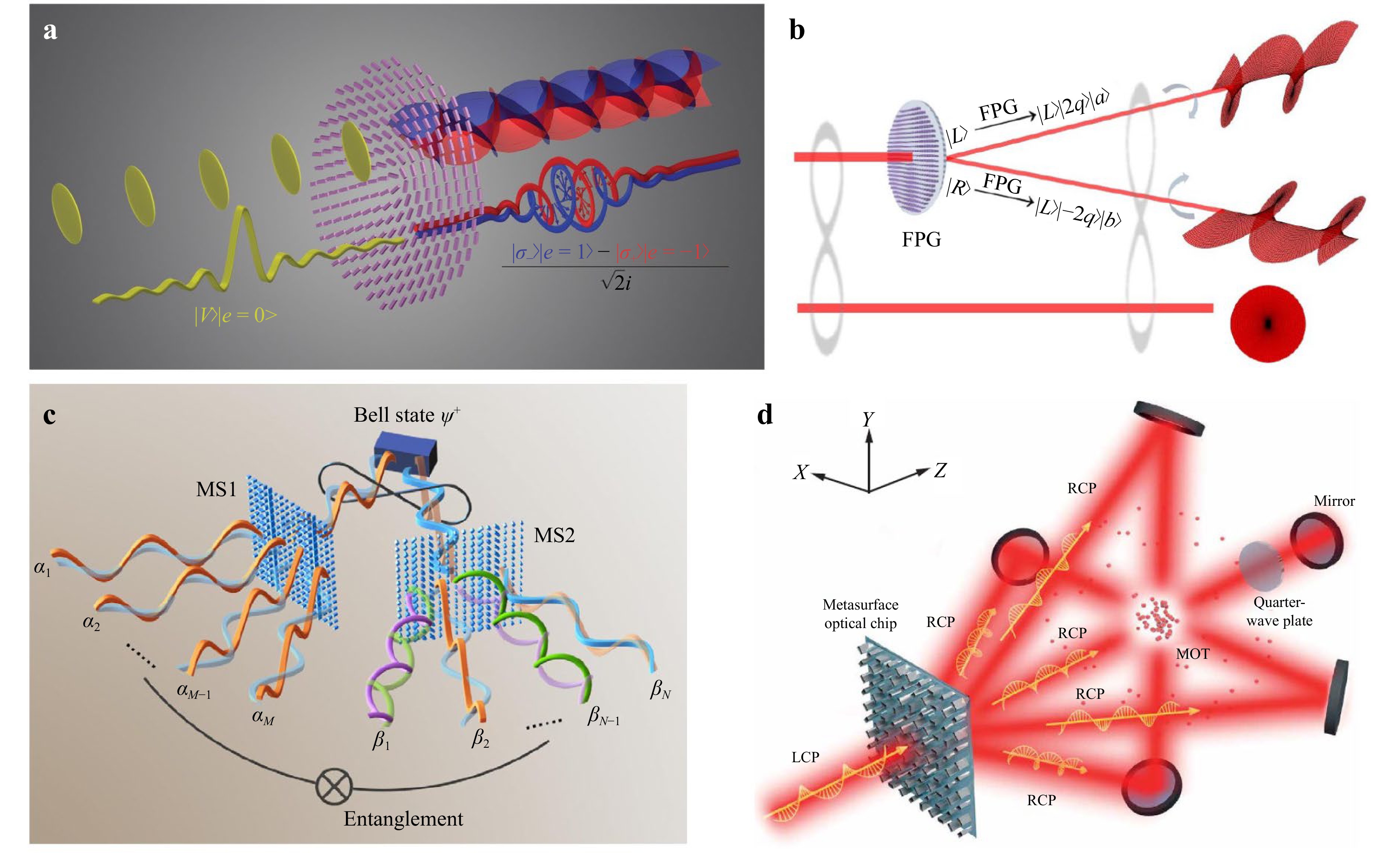
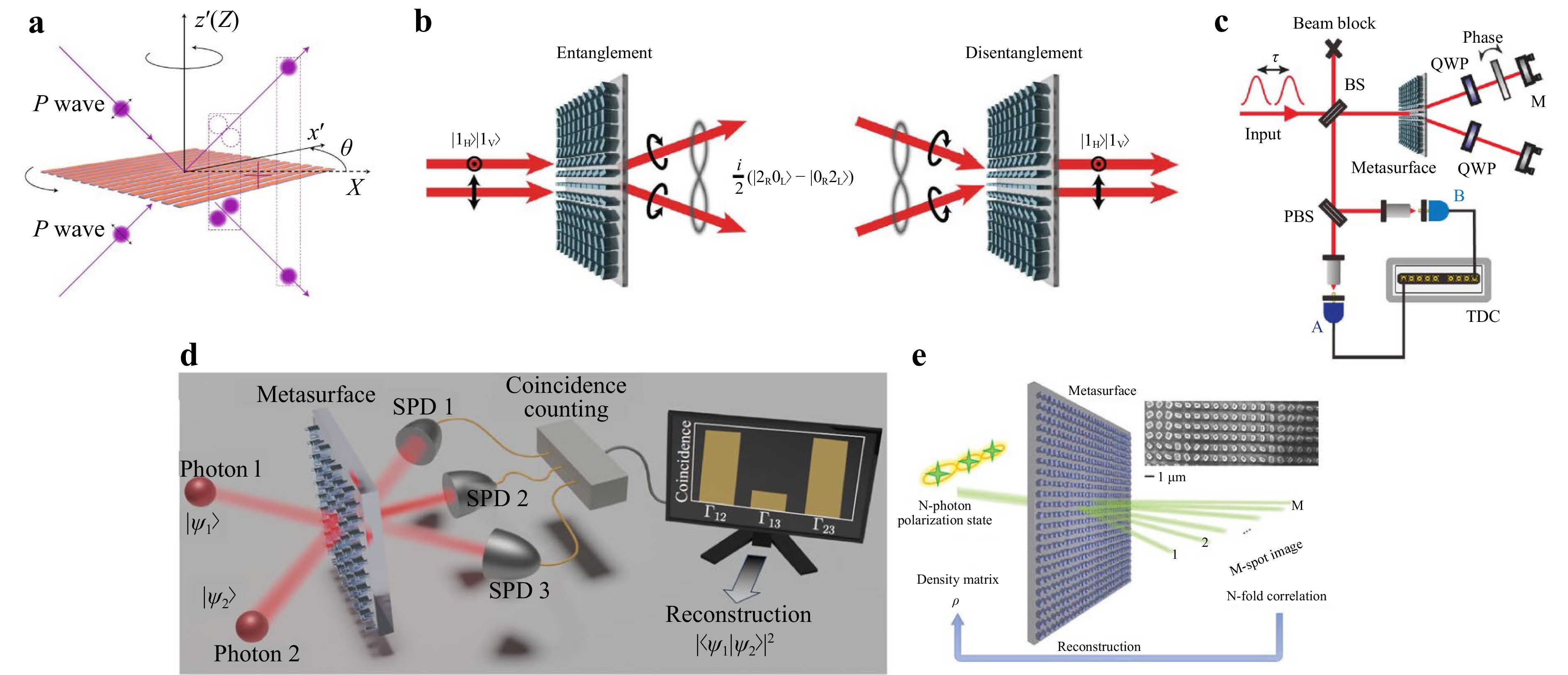
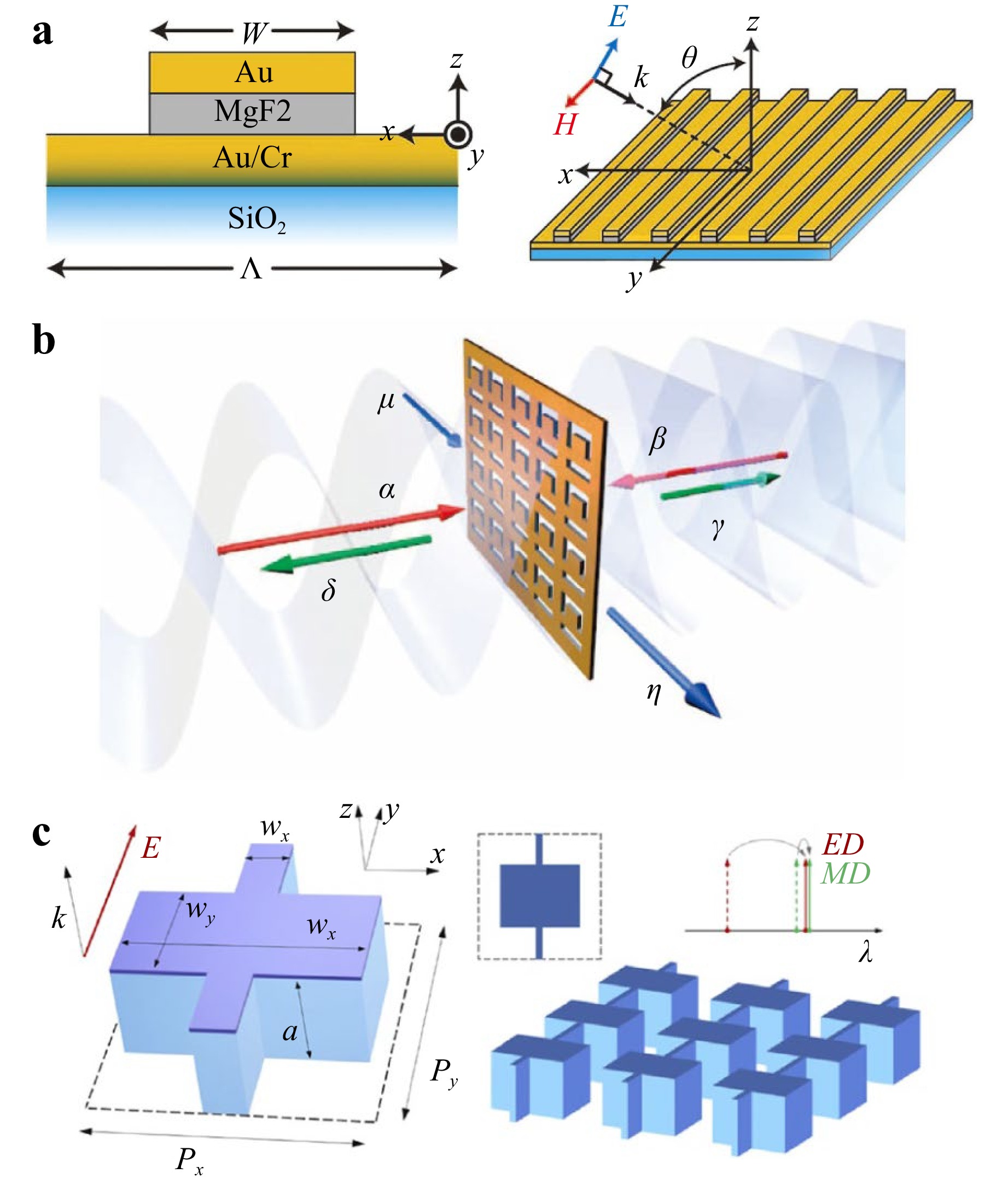
Meta-devices, known for their capability to manipulate light fields at a subwavelength scale, have gained significant traction in the realm of quantum photonics in recent years. They are being utilized in miniaturized applications such as the preparation of quantum light sources and the control and detection of quantum states. In this review, we provide a systematic explanation of the working principles and notable applications of meta-devices in quantum optical information processing, while also outlining potential directions for the future development of quantum meta-devices.
Published
, Published online: 21 August 2025
, doi: 10.37188/lam.2025.058
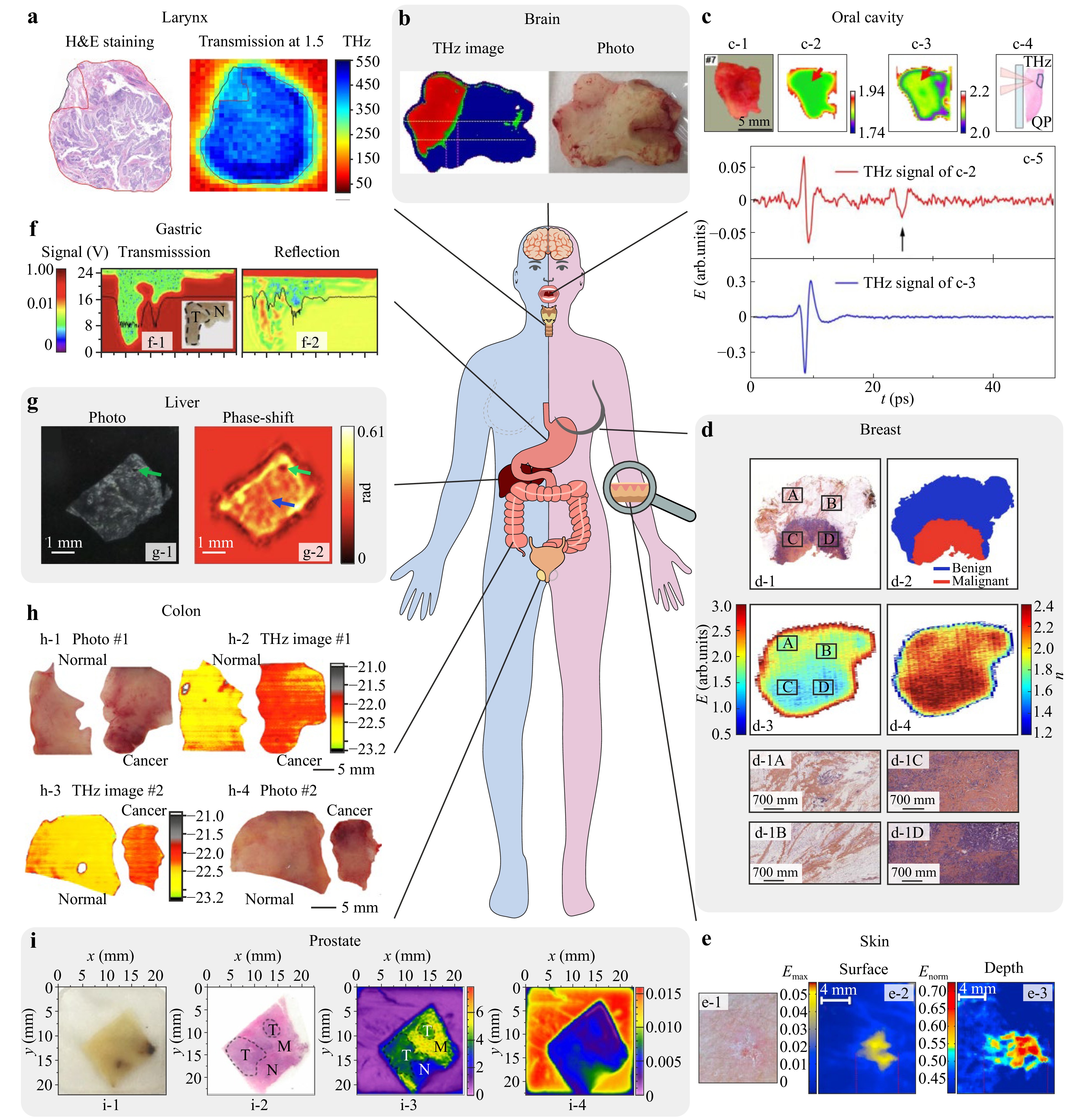
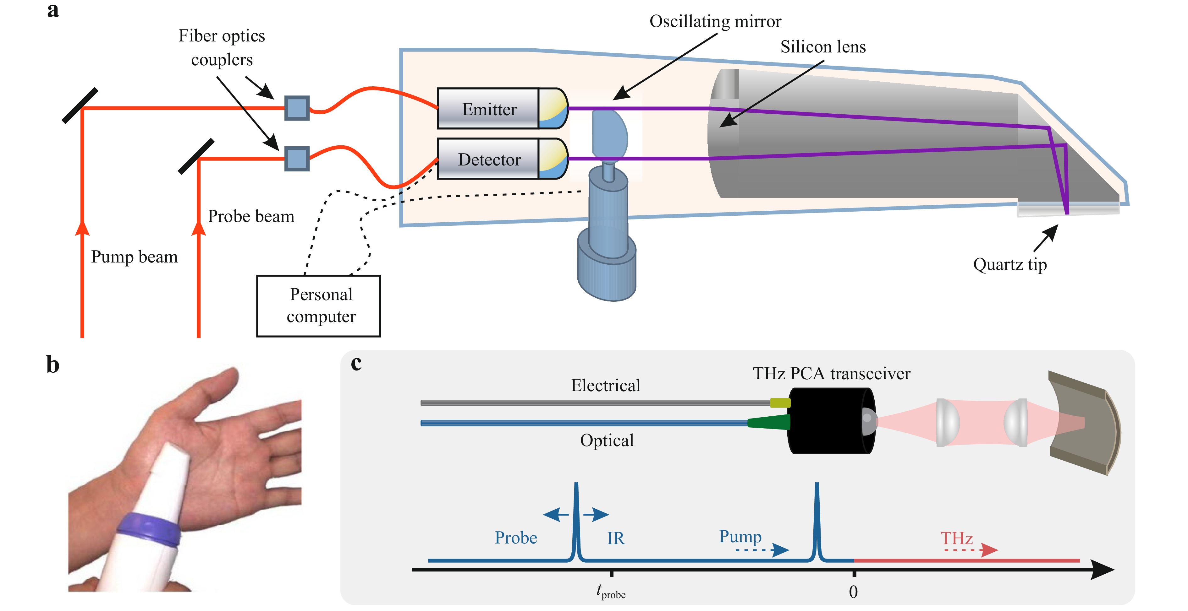
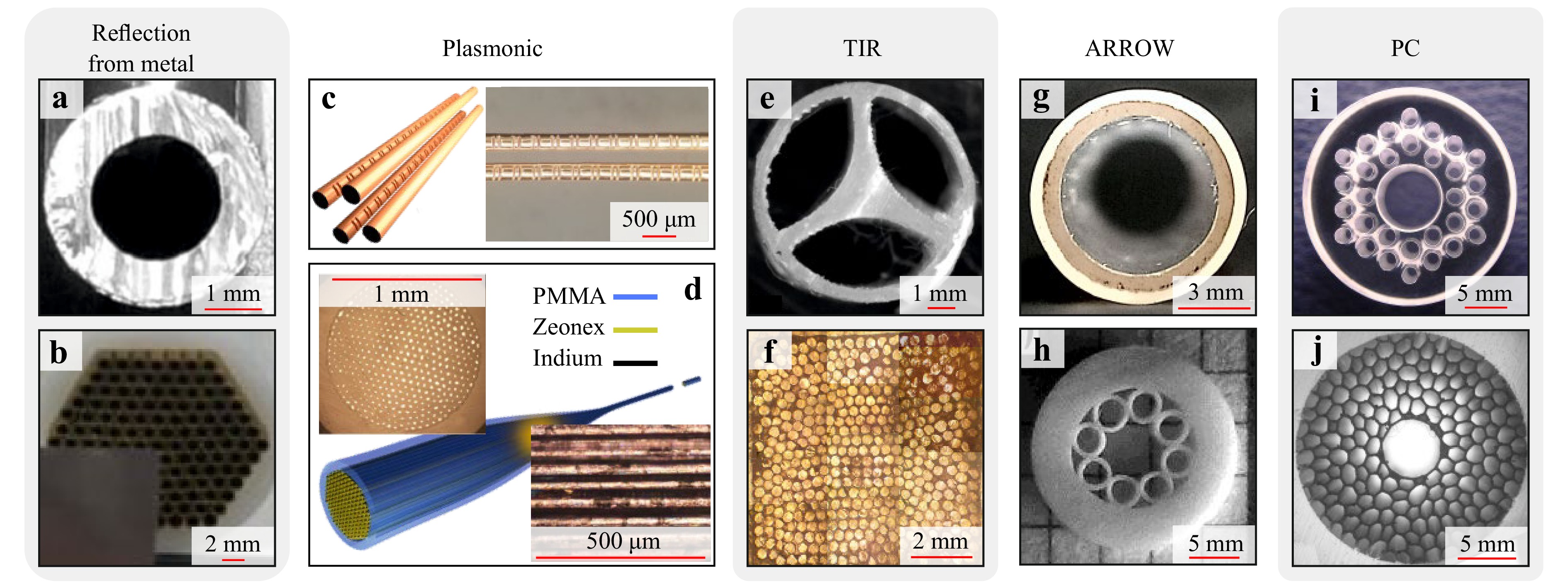
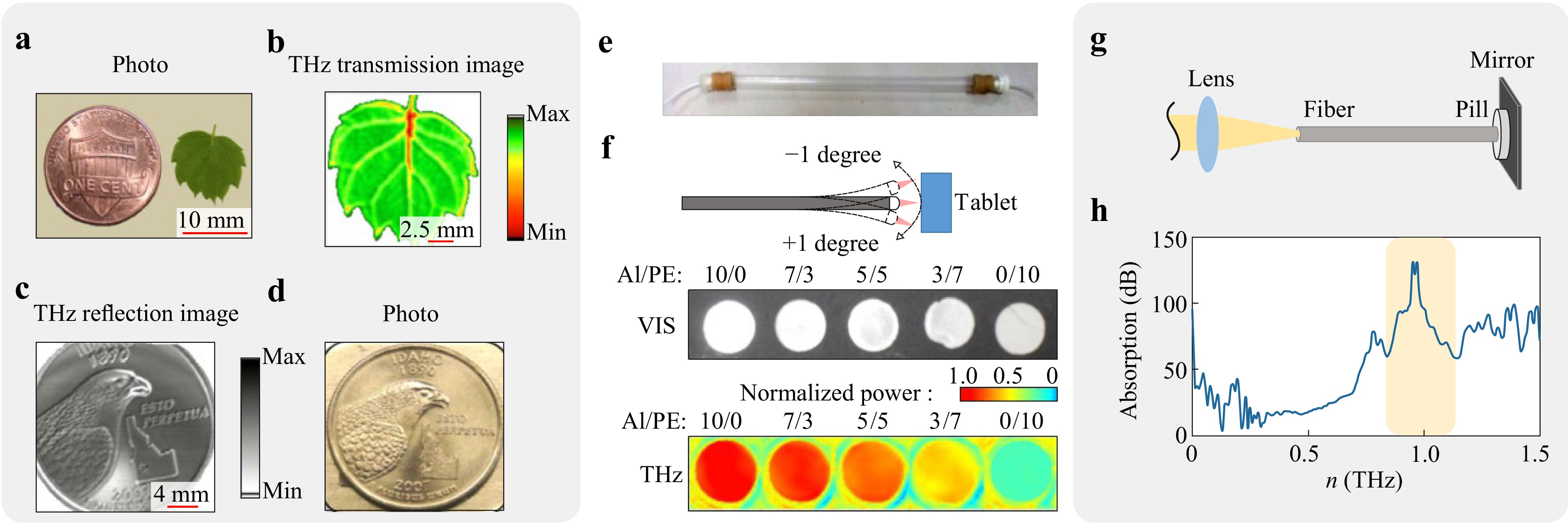
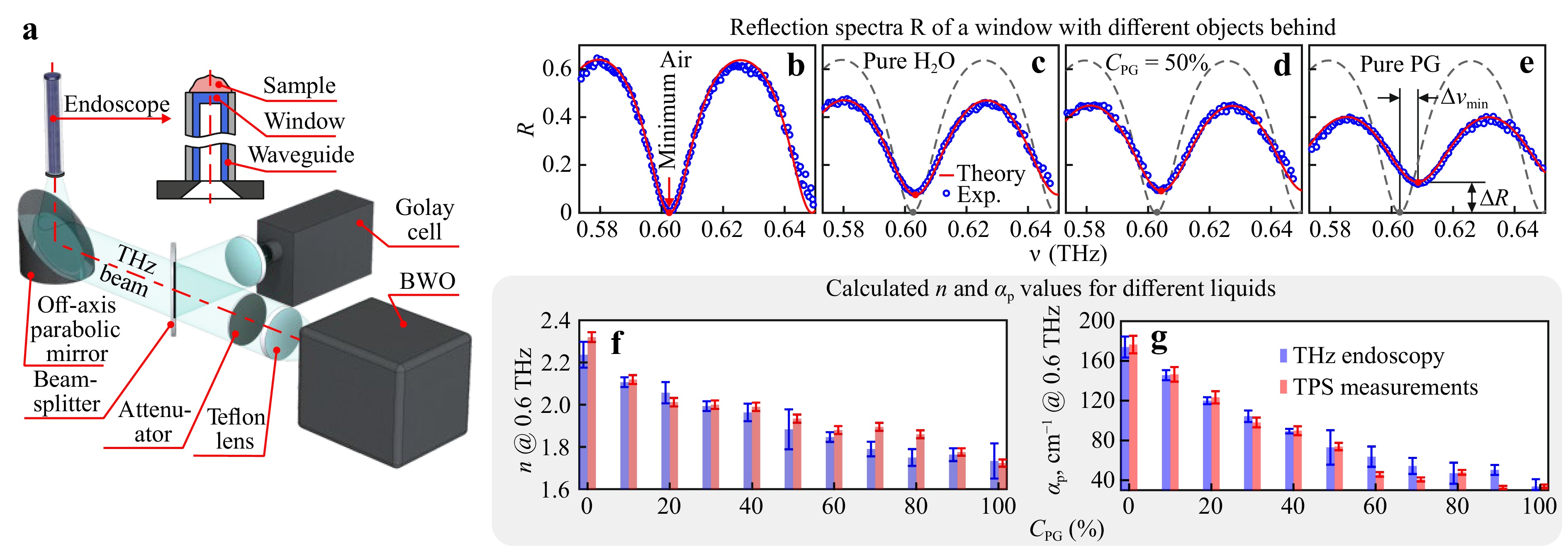
Although terahertz (THz) spectroscopy and imaging offer a variety of applications in medical diagnosis of malignant and benign neoplasms, their translation into clinical practice is hampered by the absence of endoscopic systems capable of sensing the THz optical properties of the hard-to-access tissues. In this review, we focus on recent attempts to address this challenge. To better highlight the need for THz endoscopes, we start with a brief overview of THz medical applications, with an emphasis on neoplasms diagnosis. We then consider the two existing principles of THz endoscopy. The first uses the fiber-coupled THz photoconductive antennas (PCAs) for the THz generation and detection in close proximity to a hard-to-access object, where optical fibers are applied to flexibly deliver the laser pump and probe beams to the THz emitter and detector. The key technology of the second approach is the THz optical fibers capable of delivering the THz waves to an analyte and then detecting the reflected and back-propagated THz signal. Despite this approach still lacking the efficient commercially available THz fiber optics, most recent developments pave the way to solve these problems. In this review, several notable examples of THz endoscopic systems based on different guiding mechanisms, material platform, and manufacturing strategies are discussed.
Published
, Published online: 05 August 2025
, doi: 10.37188/lam.2025.049
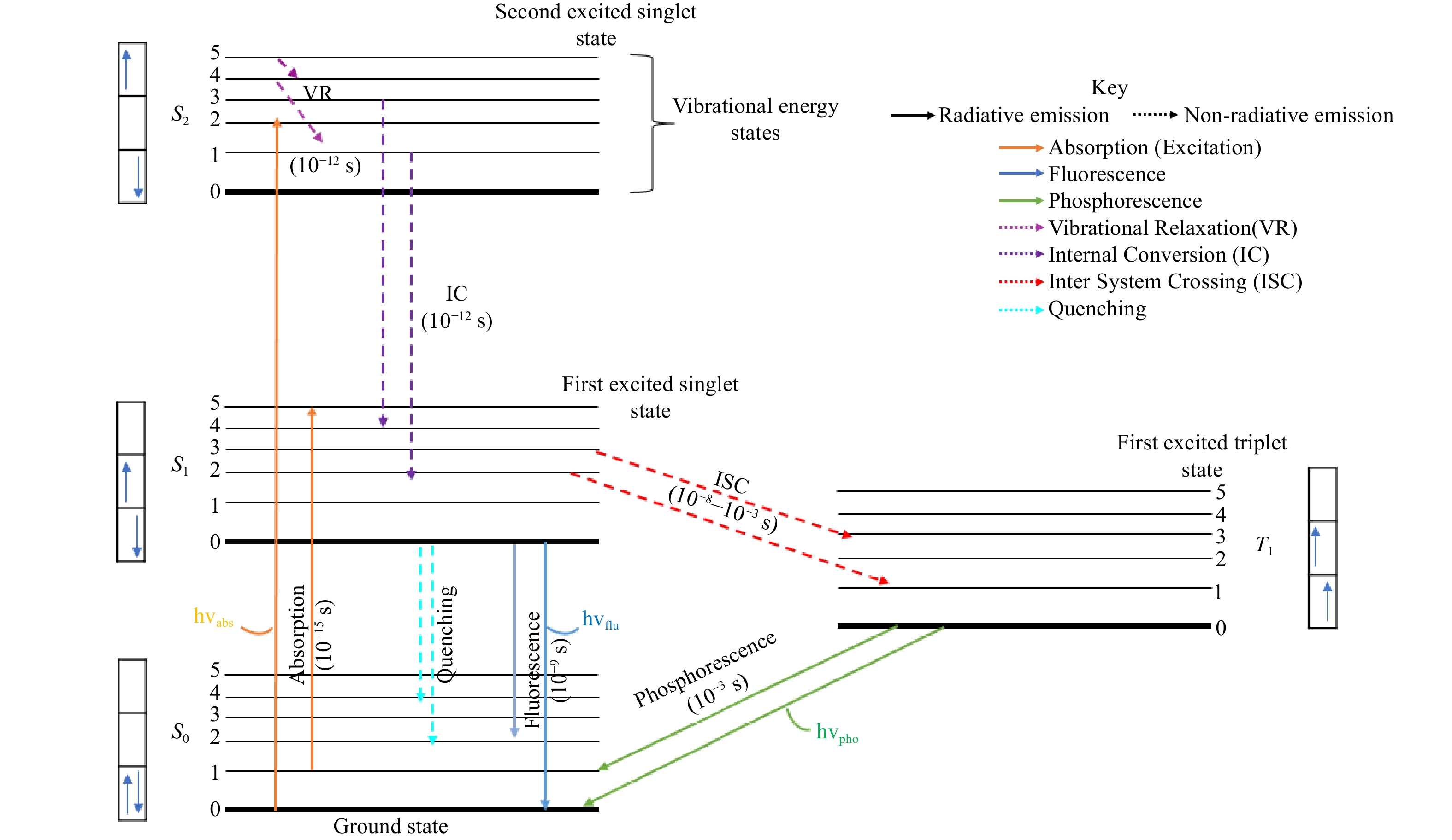
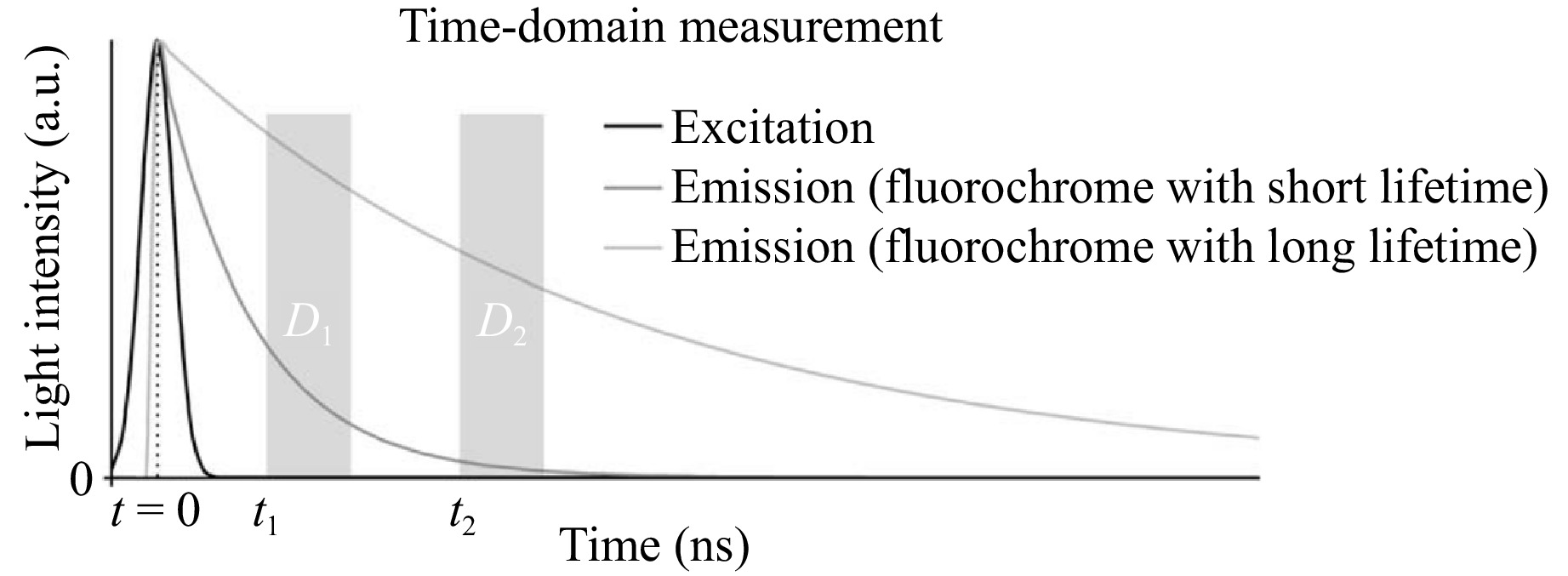
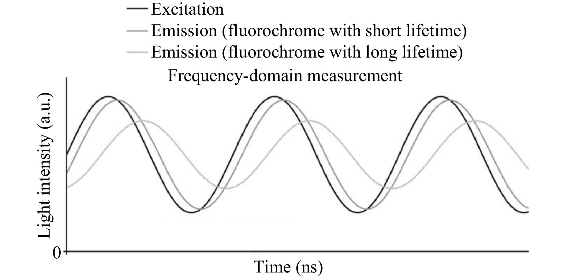
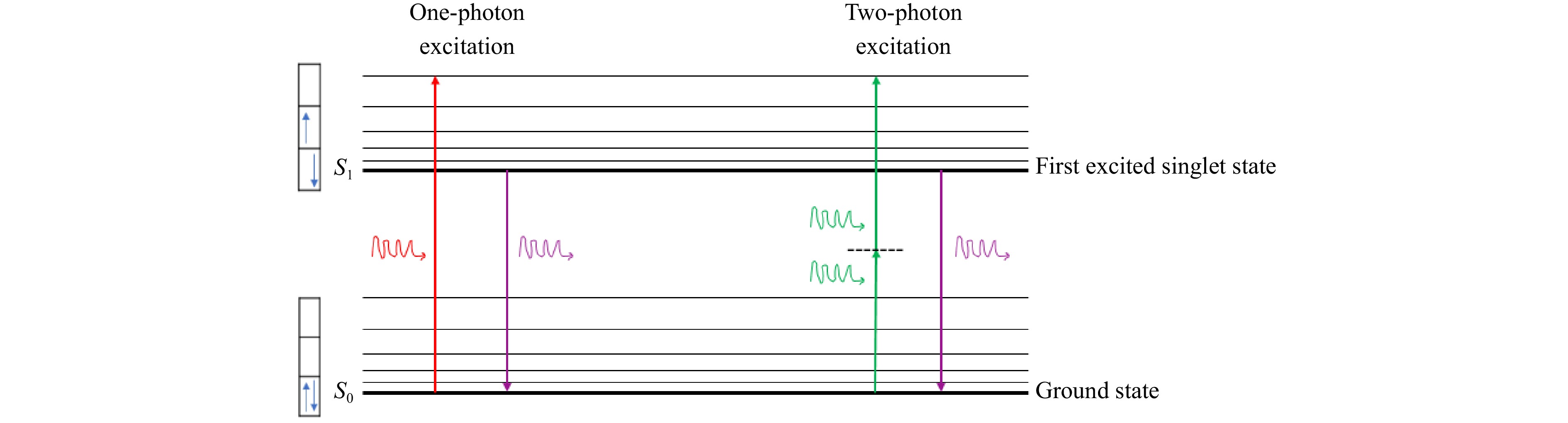
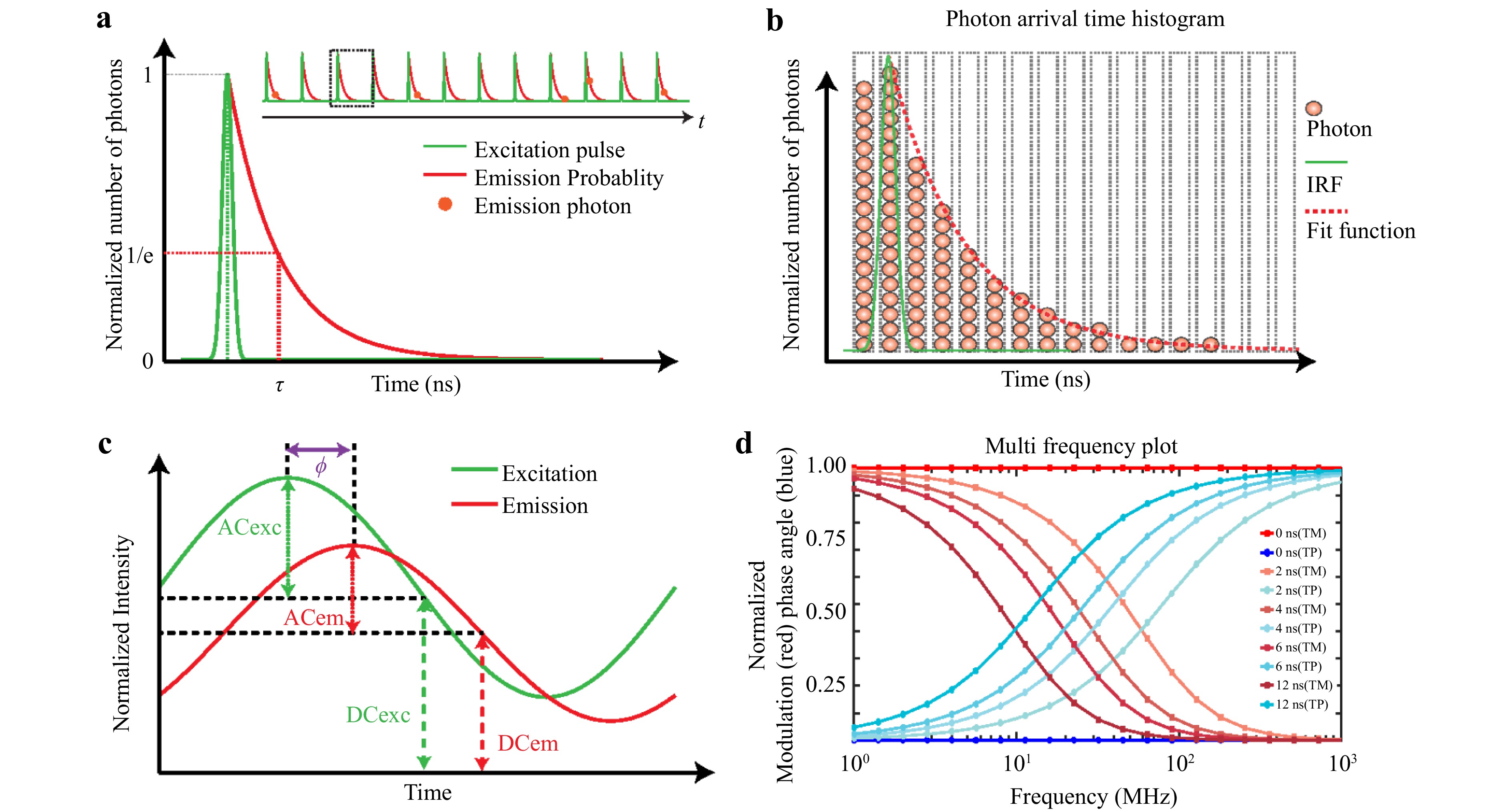
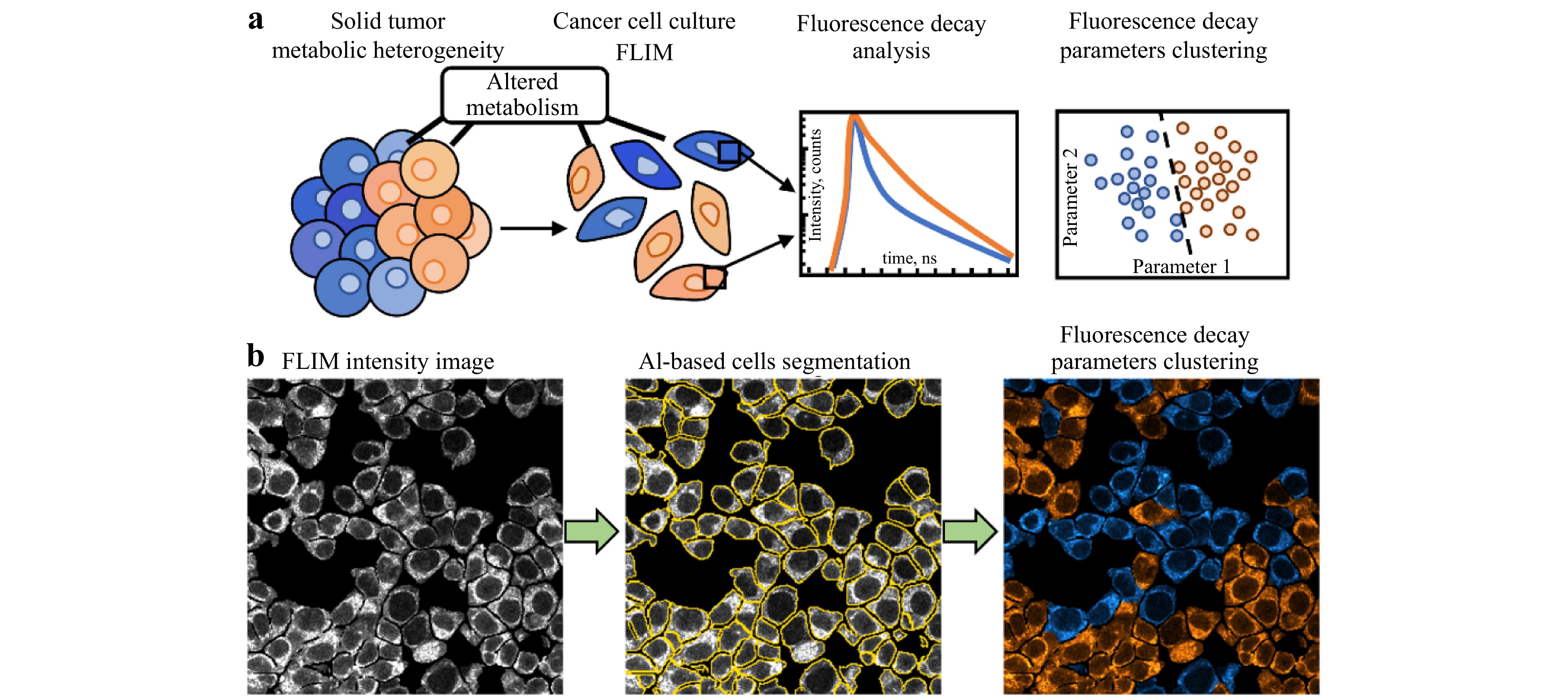
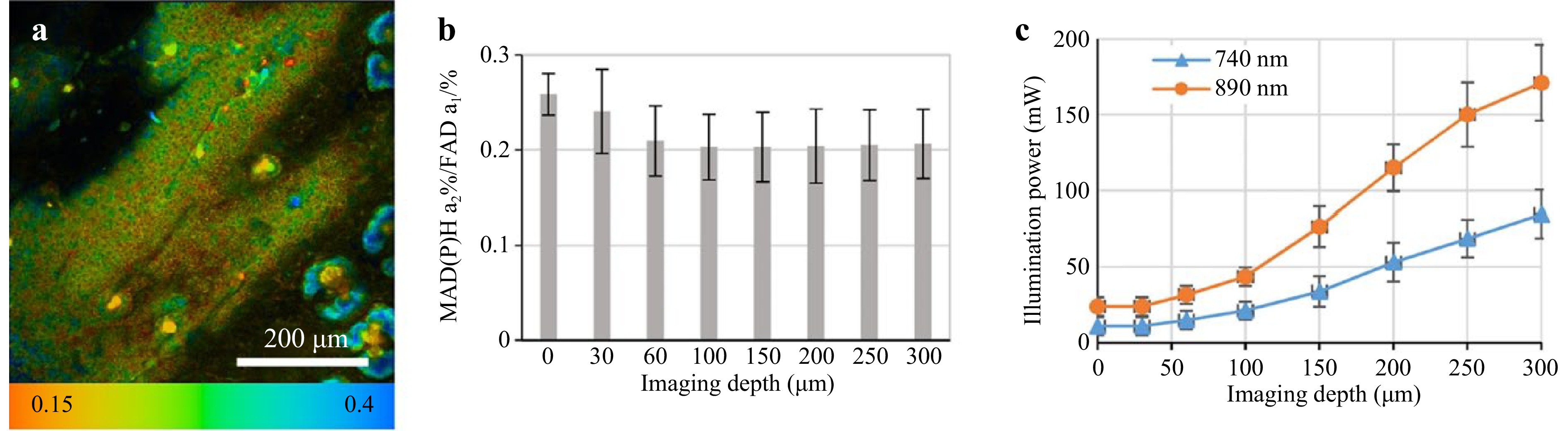
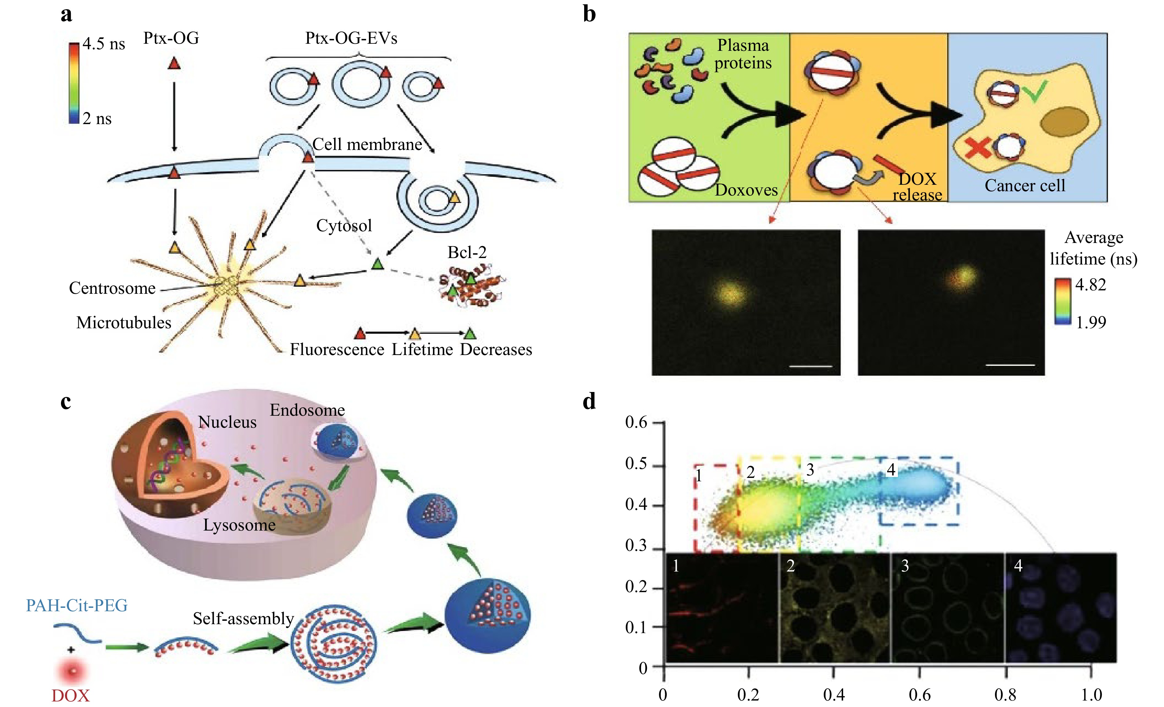
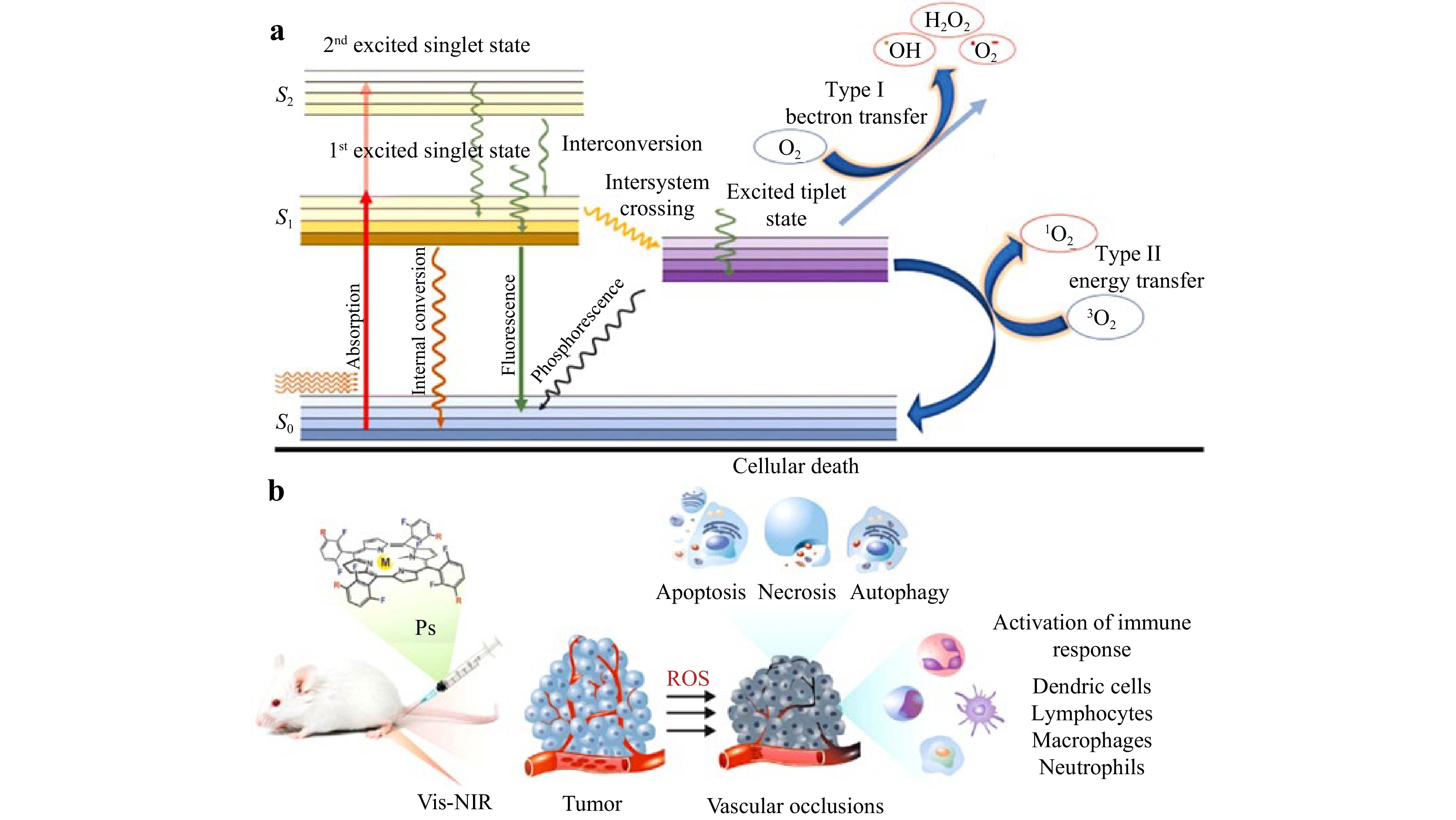
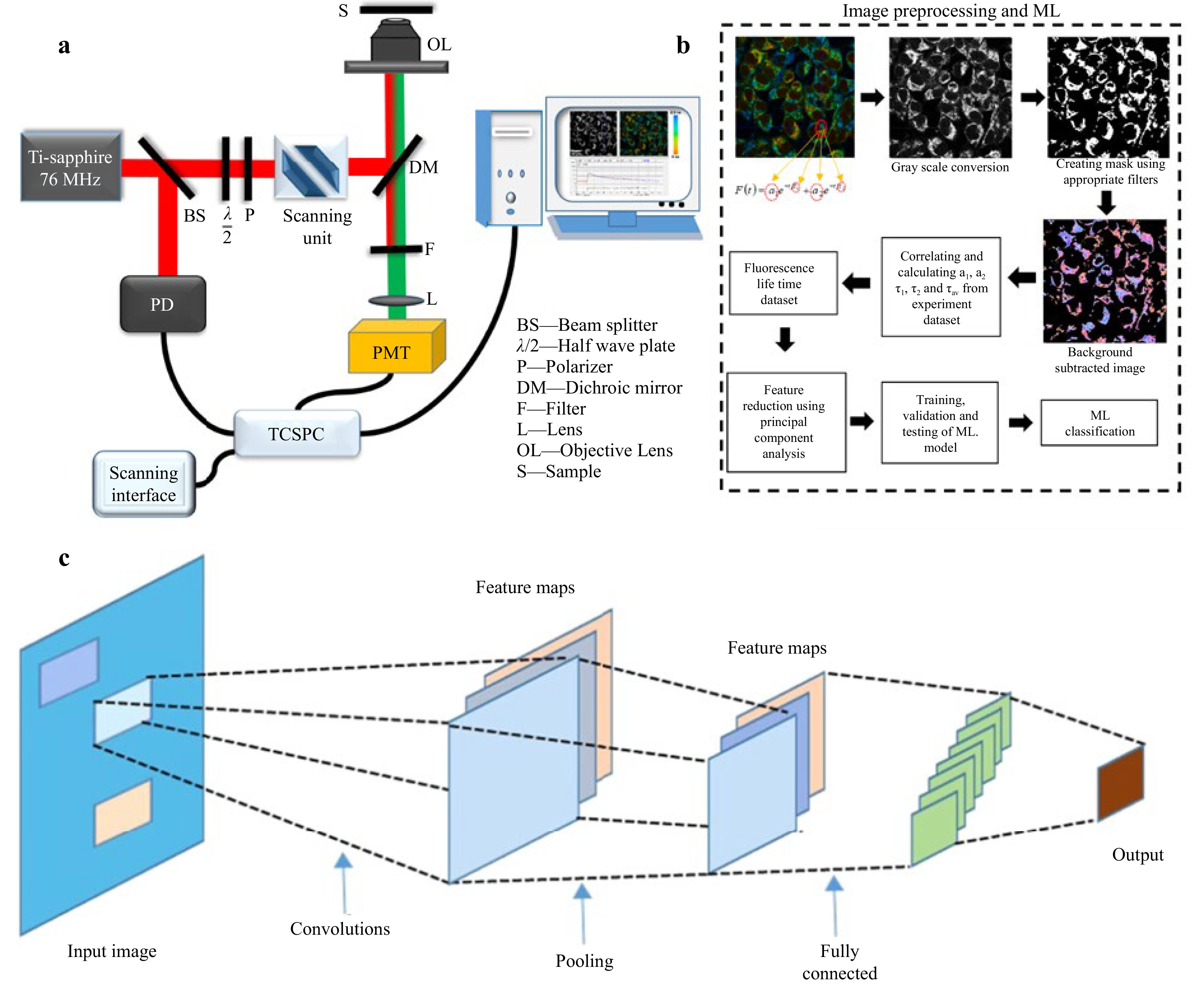
Fluorescence lifetime imaging microscopy (FLIM) has emerged as a transformative imaging technique in cancer research, offering quantitative insights into cellular metabolism, tumor microenvironments, and therapeutic responses. By measuring the fluorescence lifetimes of metabolic cofactors such as NADH and FAD, FLIM facilitates the analysis of cancer-specific metabolic reprogramming and heterogeneity. Integration with deep learning further enhances FLIM’s diagnostic and therapeutic potential, enabling high-resolution imaging, automated data analysis, and biomarker identification. This review provides a comprehensive overview of the principles and technological advancements of FLIM, highlighting its applications in cancer diagnostics, drug delivery, and therapy, as well as its integration with deep learning to increase imaging precision and data interpretation. Challenges such as high costs, high computational complexity, and the need for standardized imaging protocols are also addressed. By bridging FLIM with cutting-edge computational techniques, this review highlights its potential to revolutionize cancer research, paving the way for early diagnosis, personalized therapies, and deeper insights into tumor biology.

Published
, Published online: 30 July 2025
, doi: 10.37188/lam.2025.048
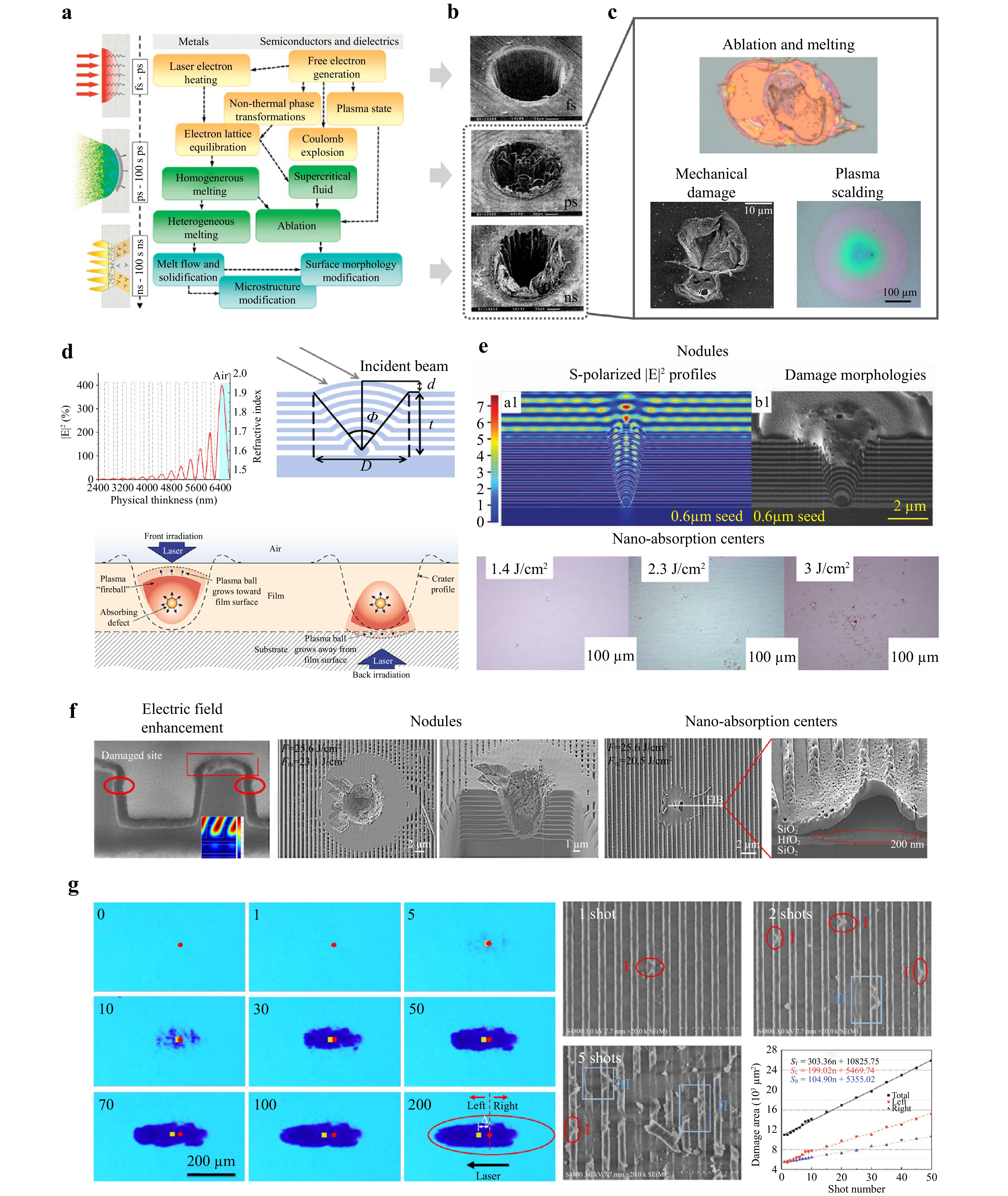
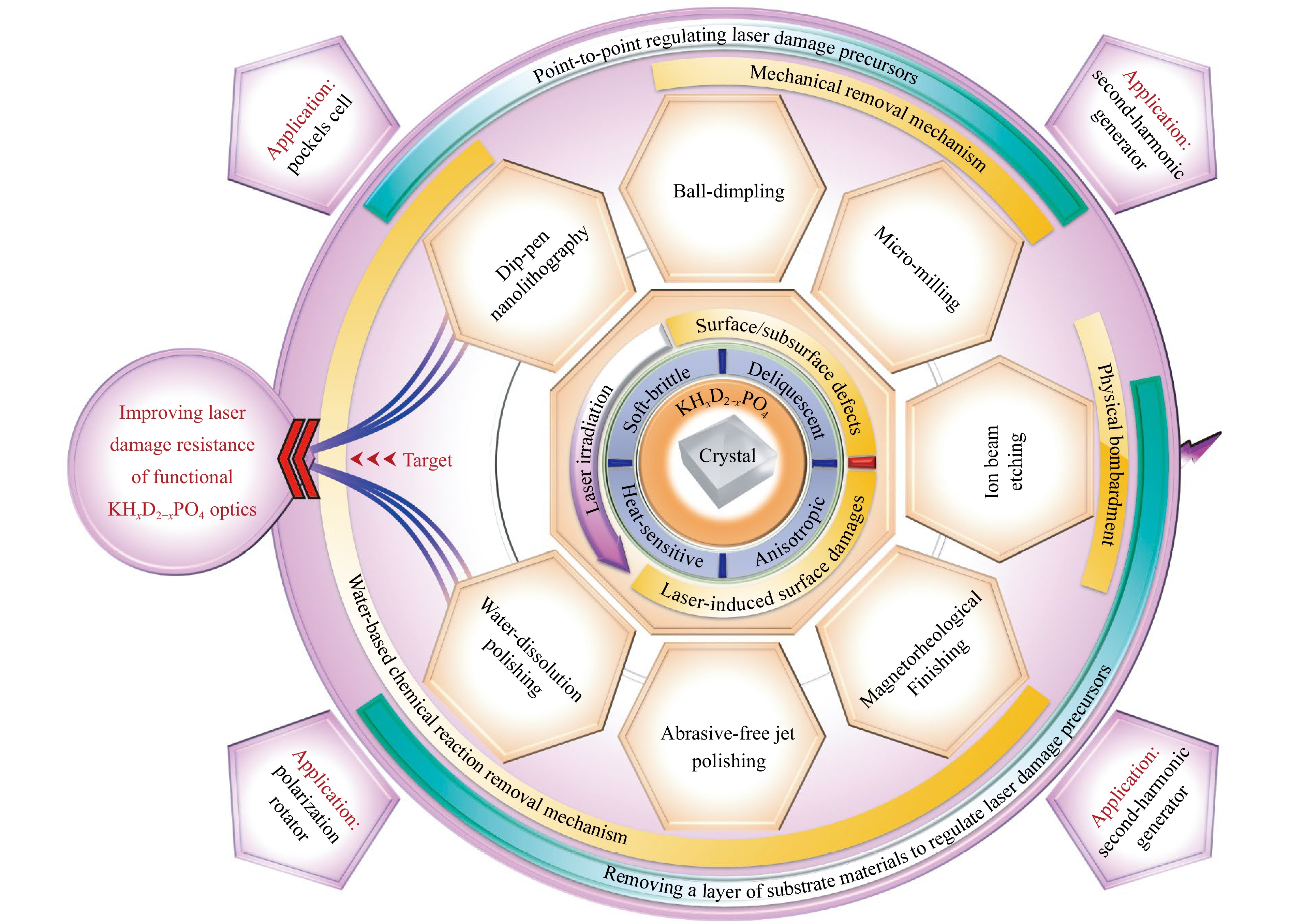
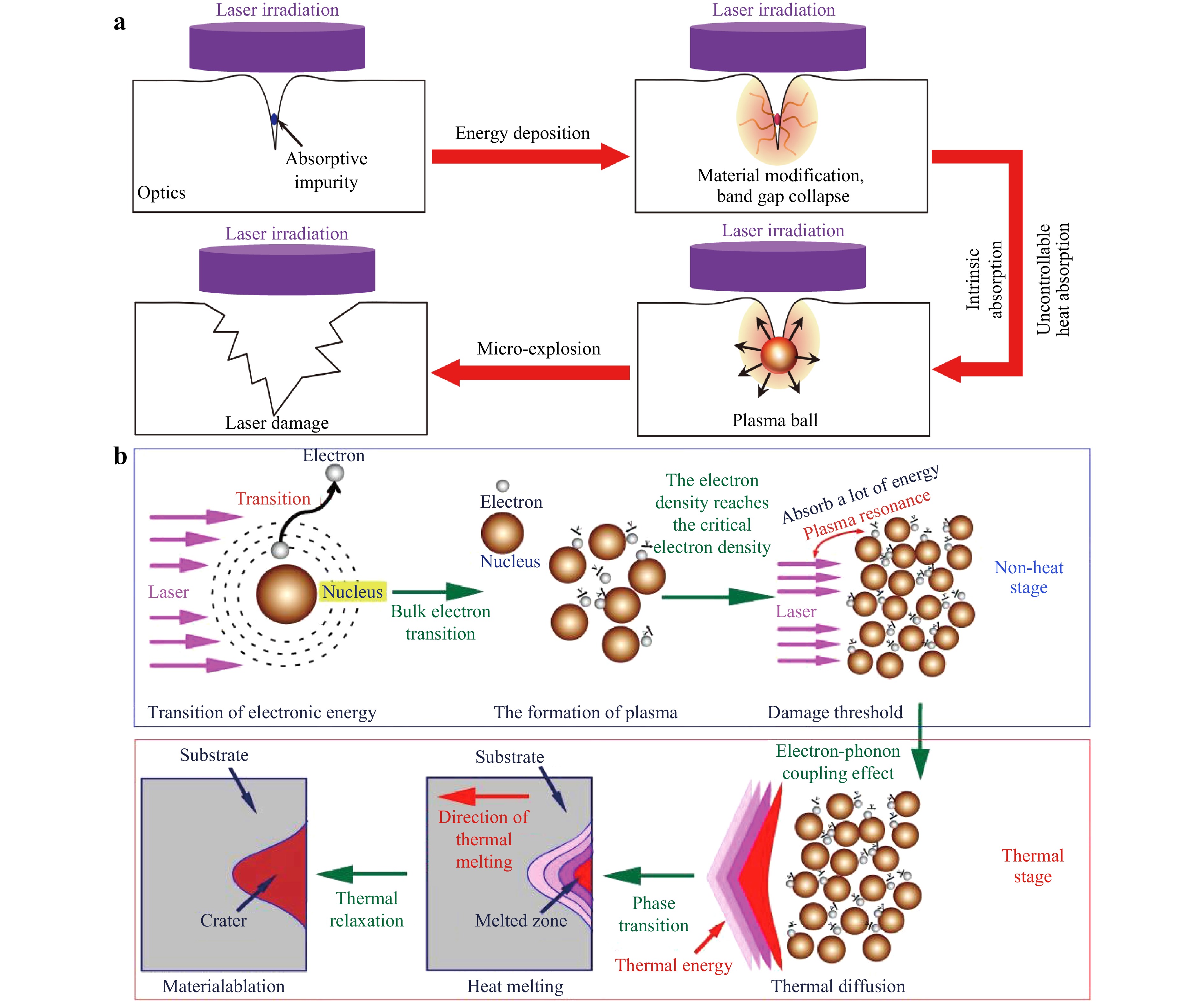
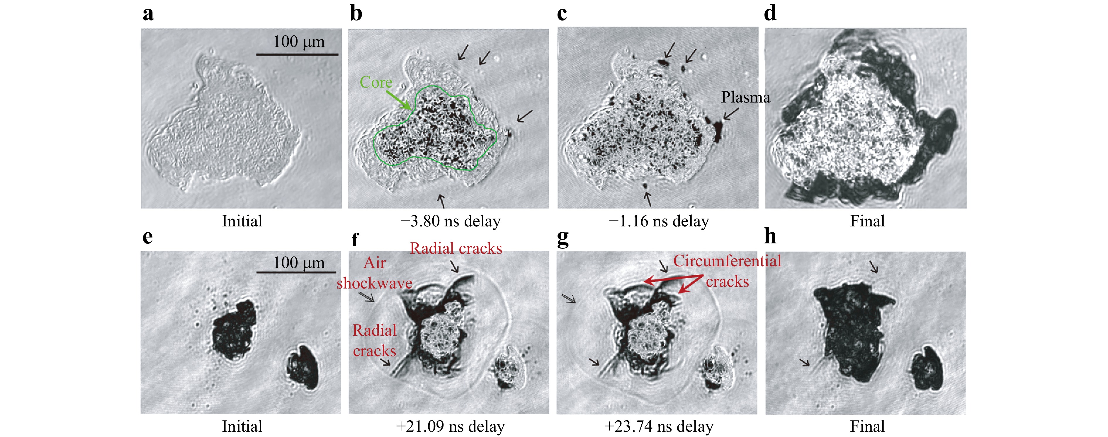
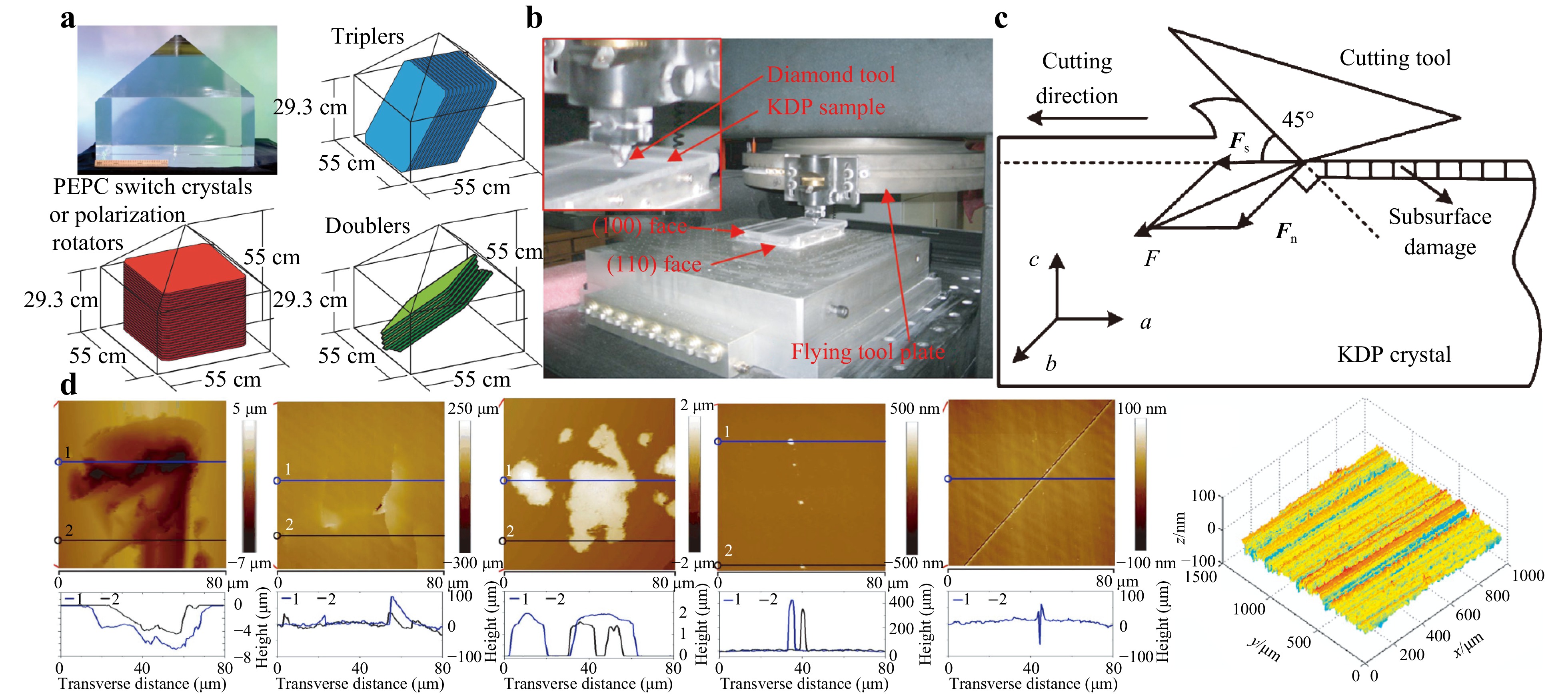
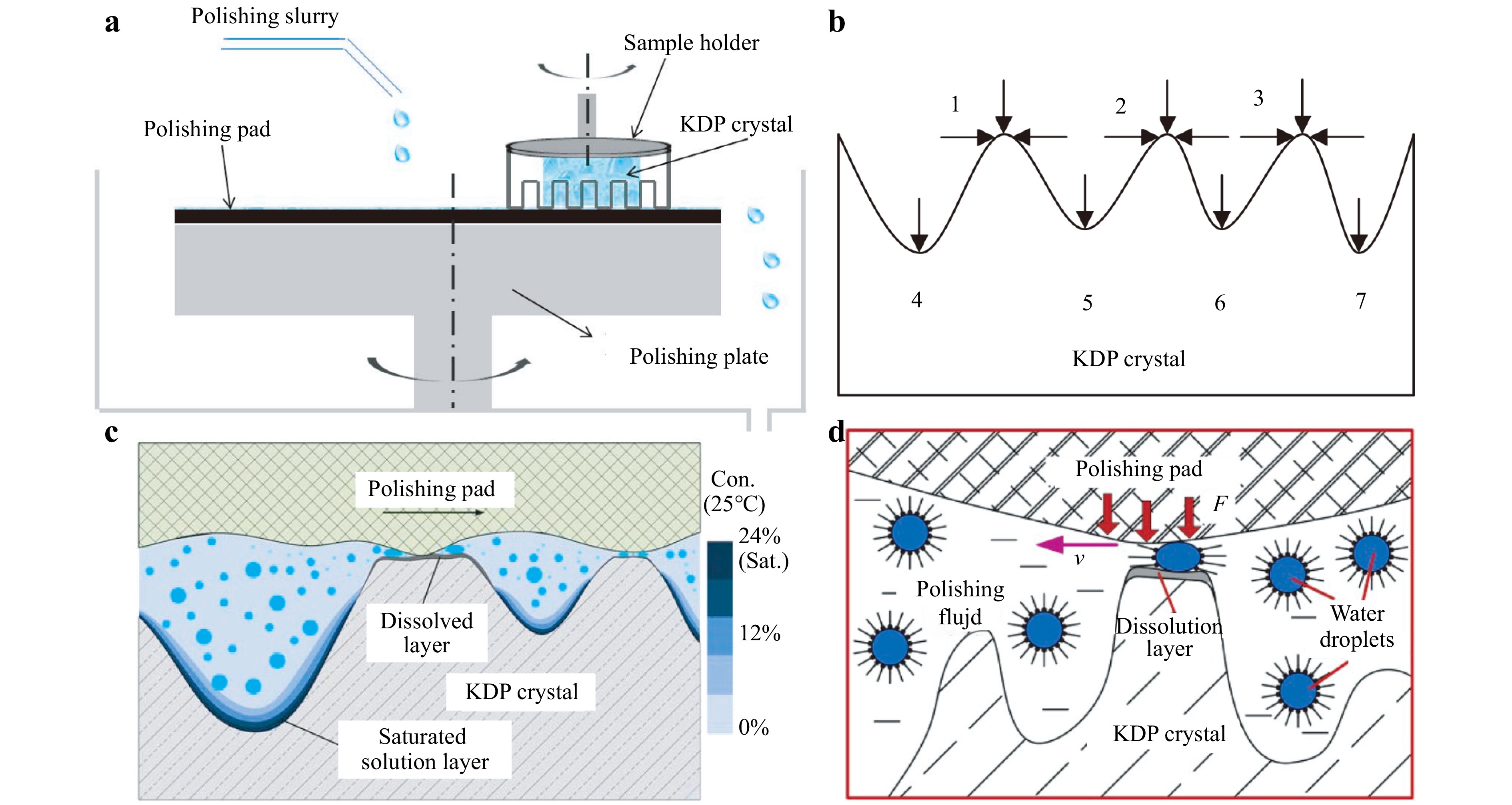
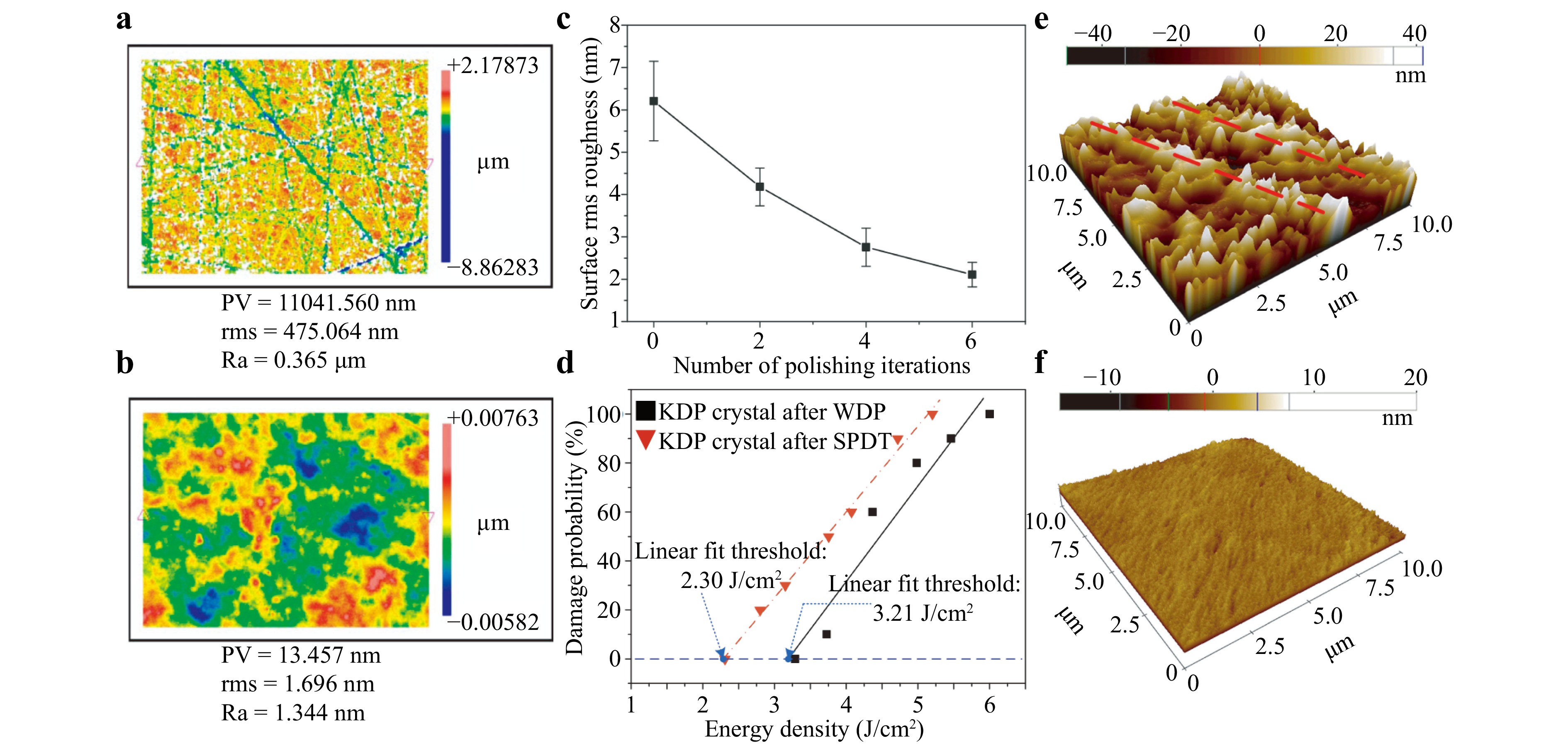
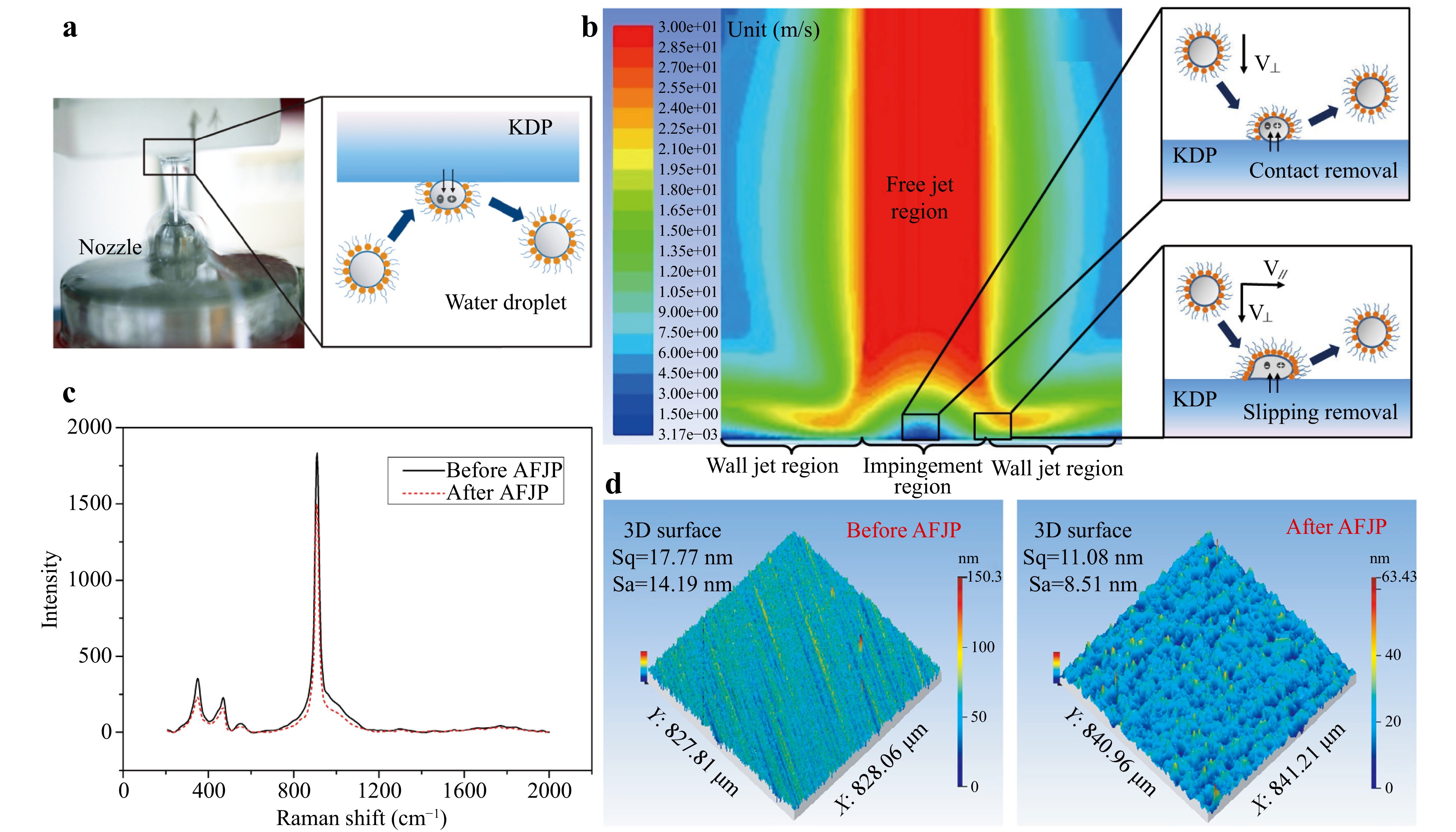
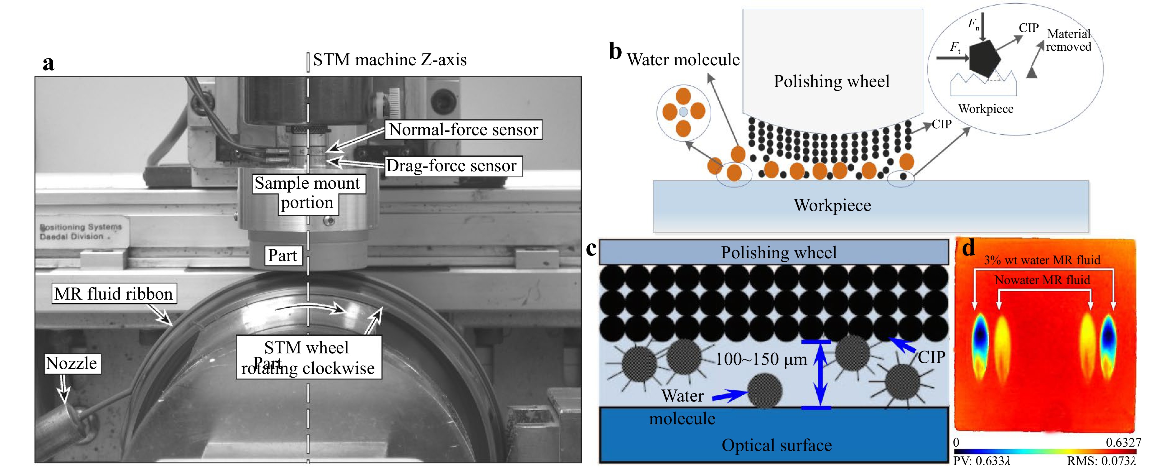
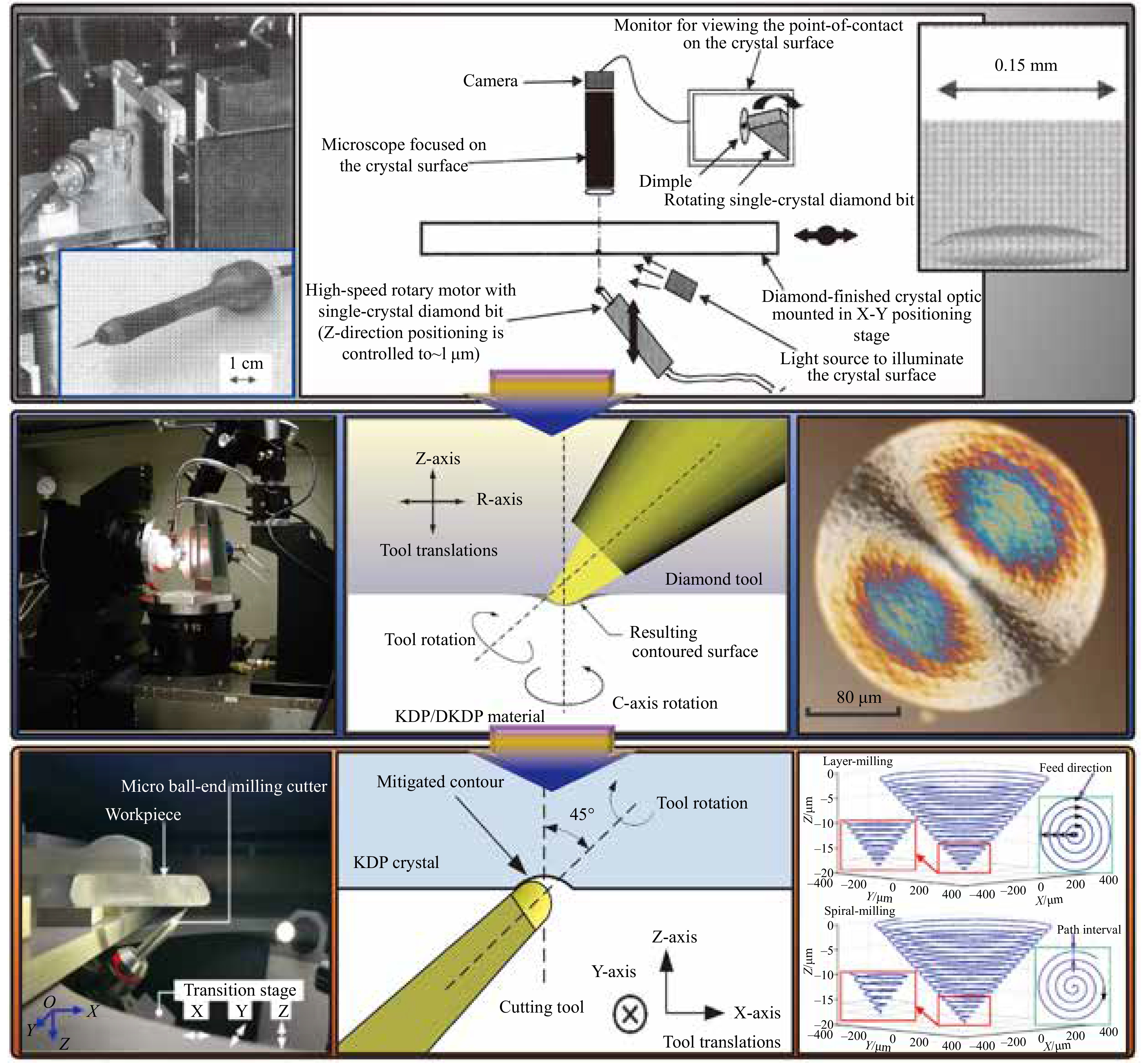
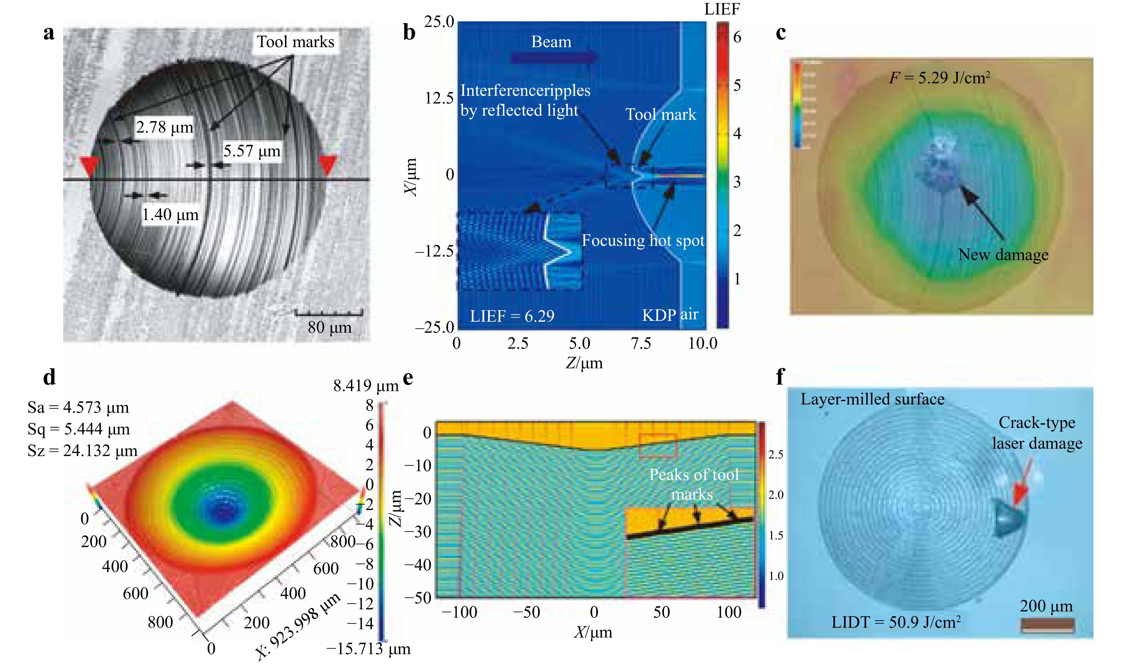
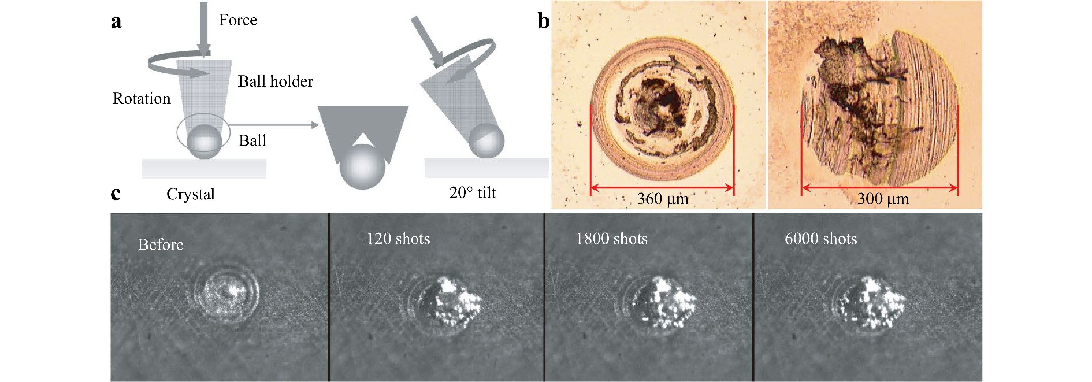
Nonlinear KHxD2-xPO4 crystal optics, e.g. second/third-harmonic generators, are components of high-energy/power laser facilities, which deliver and convert 1ω, 2ω, and 3ω lasers to obtain extreme fusion ignition conditions (high pressures, high temperatures, etc.). A laser facility requires extremely high-precision and defect-free KHxD2-xPO4 optics with meter-sized apertures to control laser beams temporally, spatially, and spectrally, yielding great ultra-precision manufacturing challenges. Meanwhile, when irradiated by intense laser pulses, laser damage precursors (e.g. manufacturing-induced micro-cracks, scratches, and debris) in the optics would spark off laser-induced surface damage and damage growth, which have been the bottleneck problems preventing the promotion of the output energies of these laser facilities. Under this circumstance, a variety of advanced optical manufacturing techniques have been developed to regulate these precursors to improve the laser damage resistance of the optics. However, the damage thresholds (8–9 J/cm2) of these optics are still far below the intrinsic threshold of the KHxD2-xPO4 (147–200 J/cm2). Furthermore, the batch engineering applications of these techniques remains challenged by the meter-sized apertures of the optics and their soft-brittle, easily deliquescent, anisotropic, and temperature-sensitive material properties, among others. This work summarises the development of state-of-the-art advanced manufacturing techniques and their problems applied in regulating laser damage precursors in the functional KHxD2-xPO4 optics. Because of their soft-brittle, deliquescent, anisotropic nature, etc., these crystal optics are difficult to cut, and new damage precursors (i.e. corrosion, debris, tool marks) could be introduced in the manufacturing processes. The challenges and their solutions are emphatically discussed and analysed in this paper. The latest development trends for the manufacture of high-performance KHxD2-xPO4 optics with high laser damage resistance are also explored. This work could provide basis and guidance for the function-oriented high-performance manufacturing of KHxD2-xPO4 optics and other functional optics with similar material properties, advancing the development of high-energy/power laser facilities.
Published
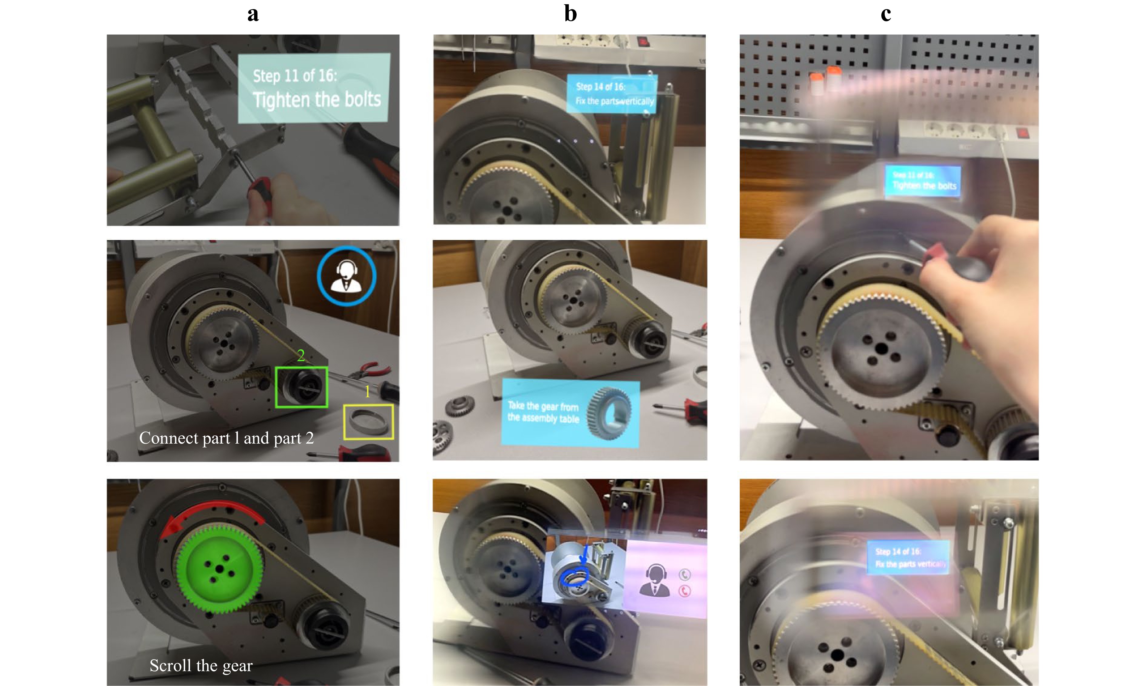
, Published online: 21 April 2025
, doi: 10.37188/lam.2025.023
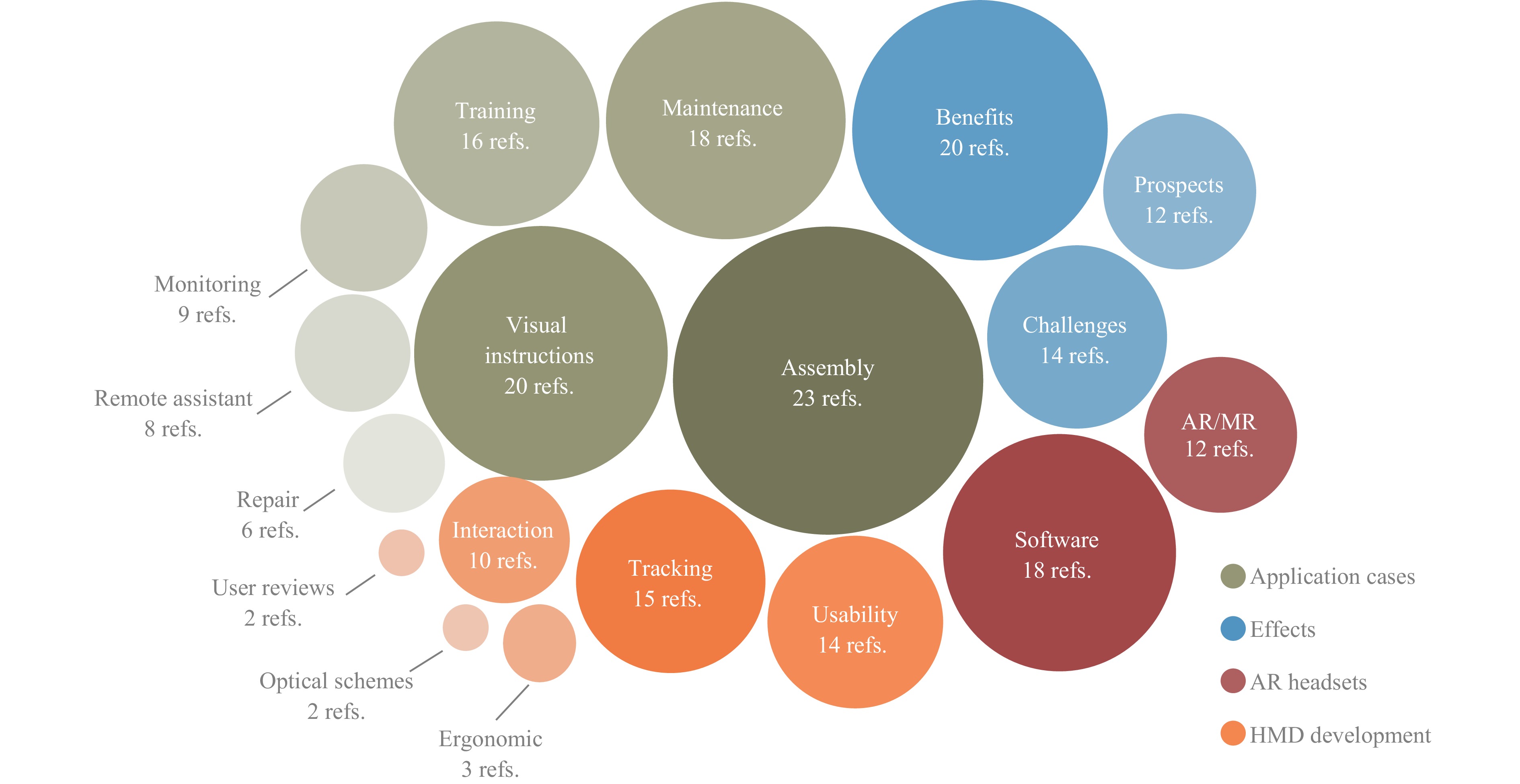
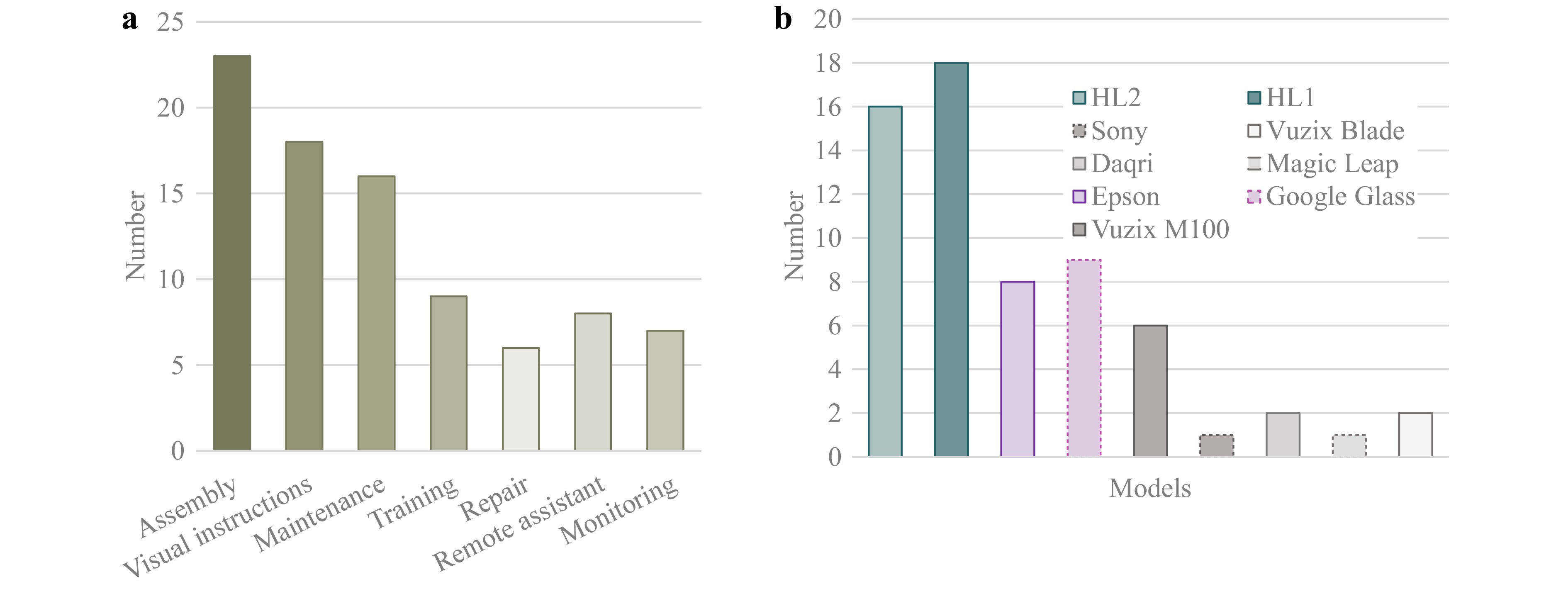
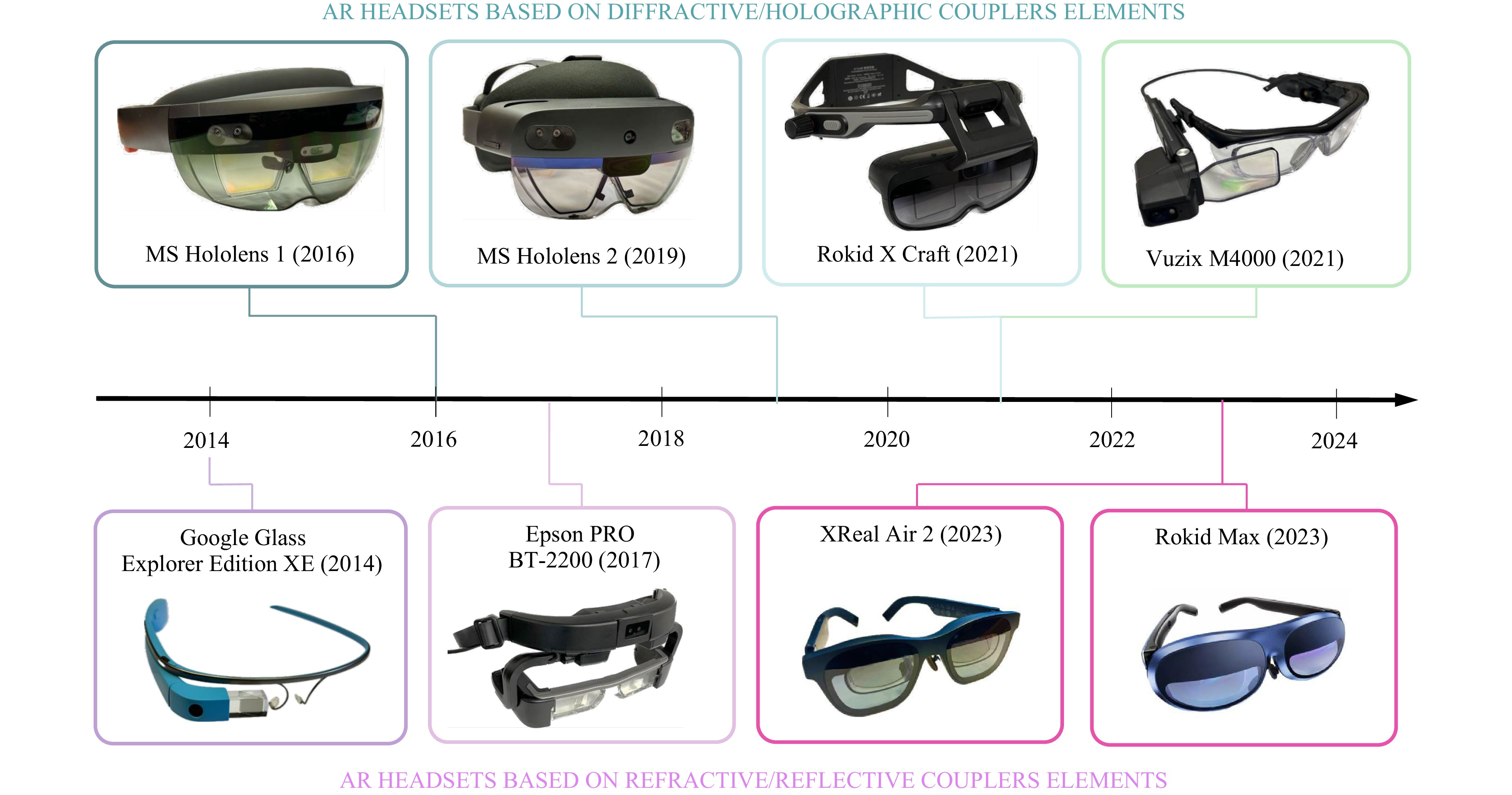
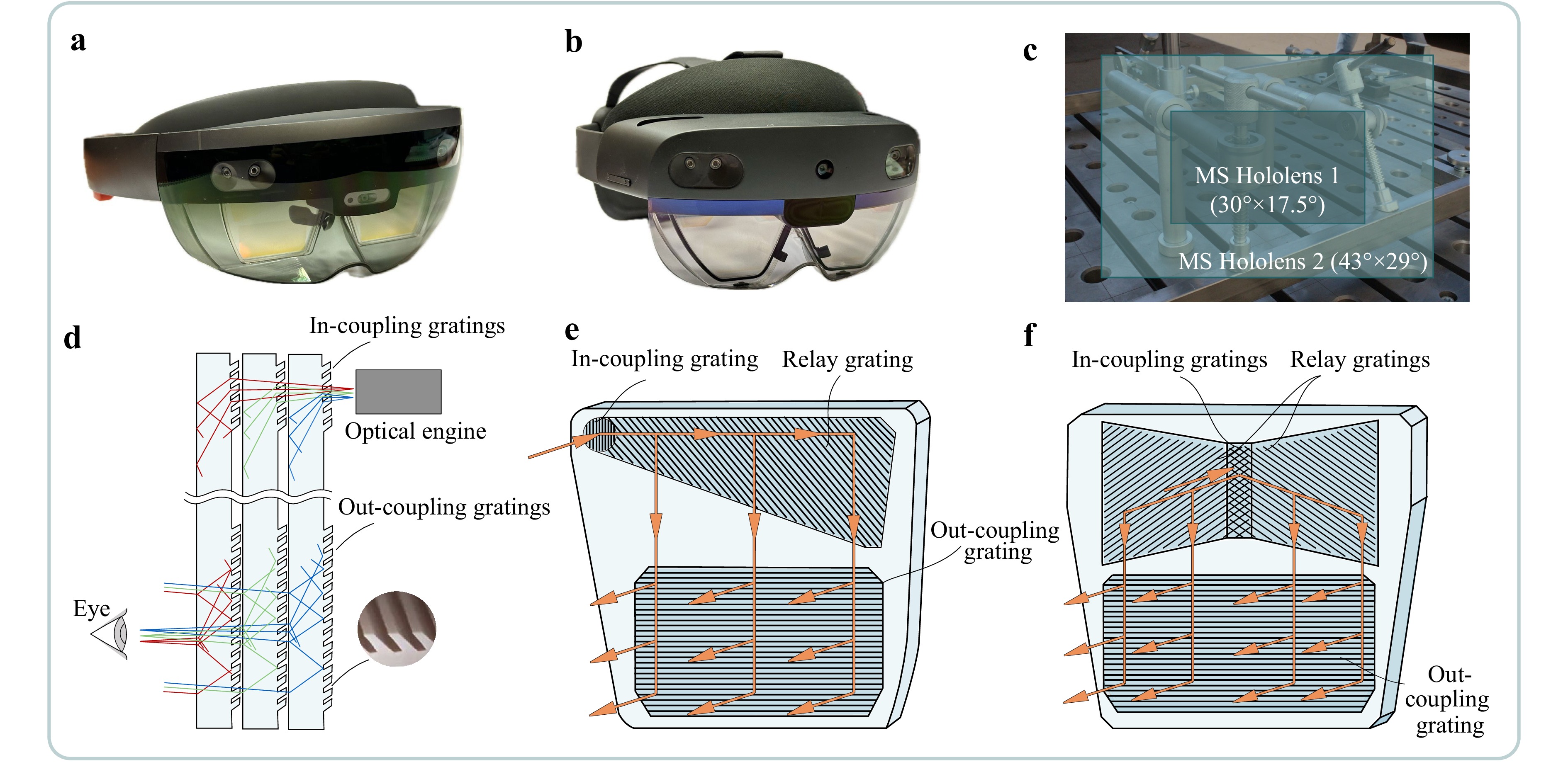
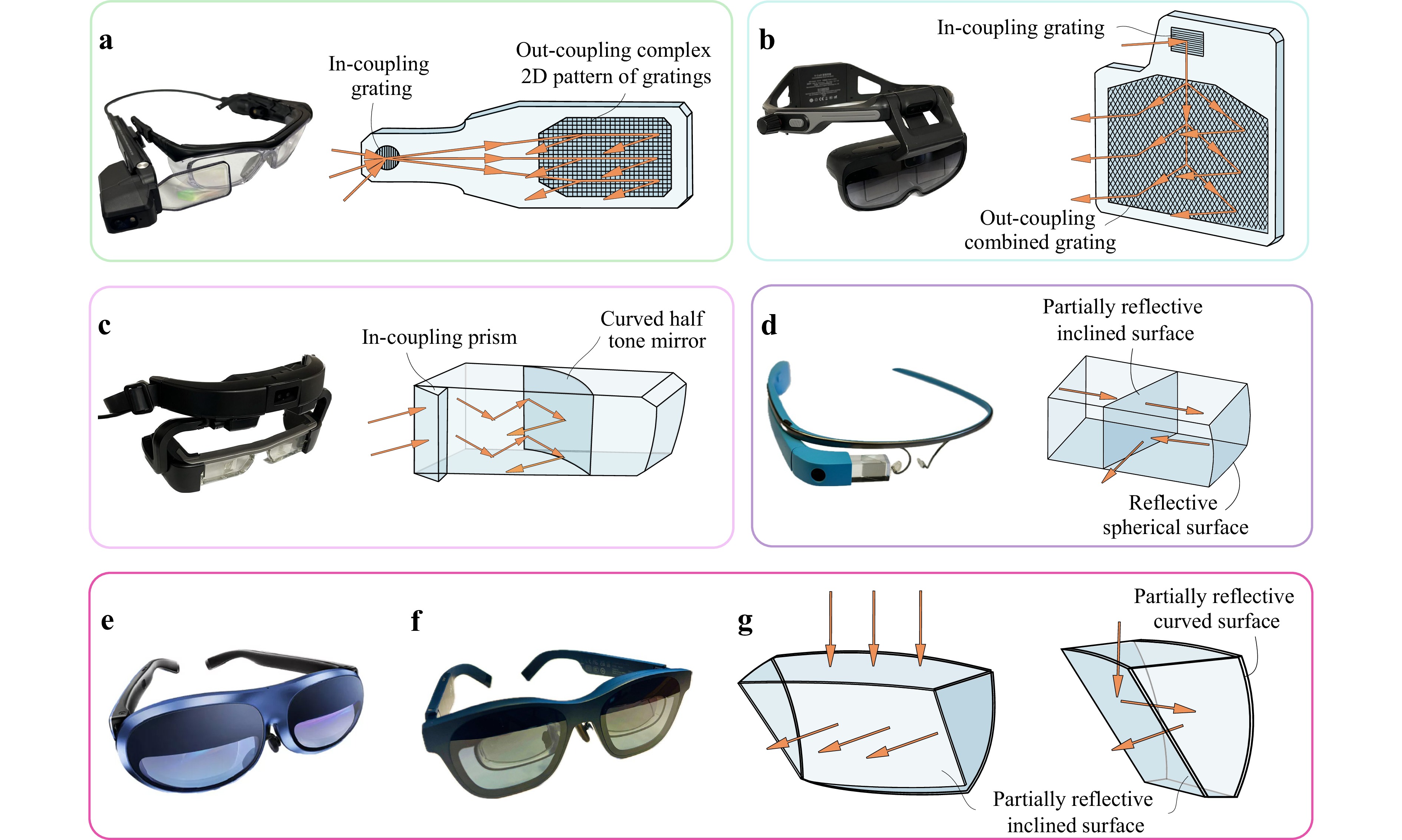
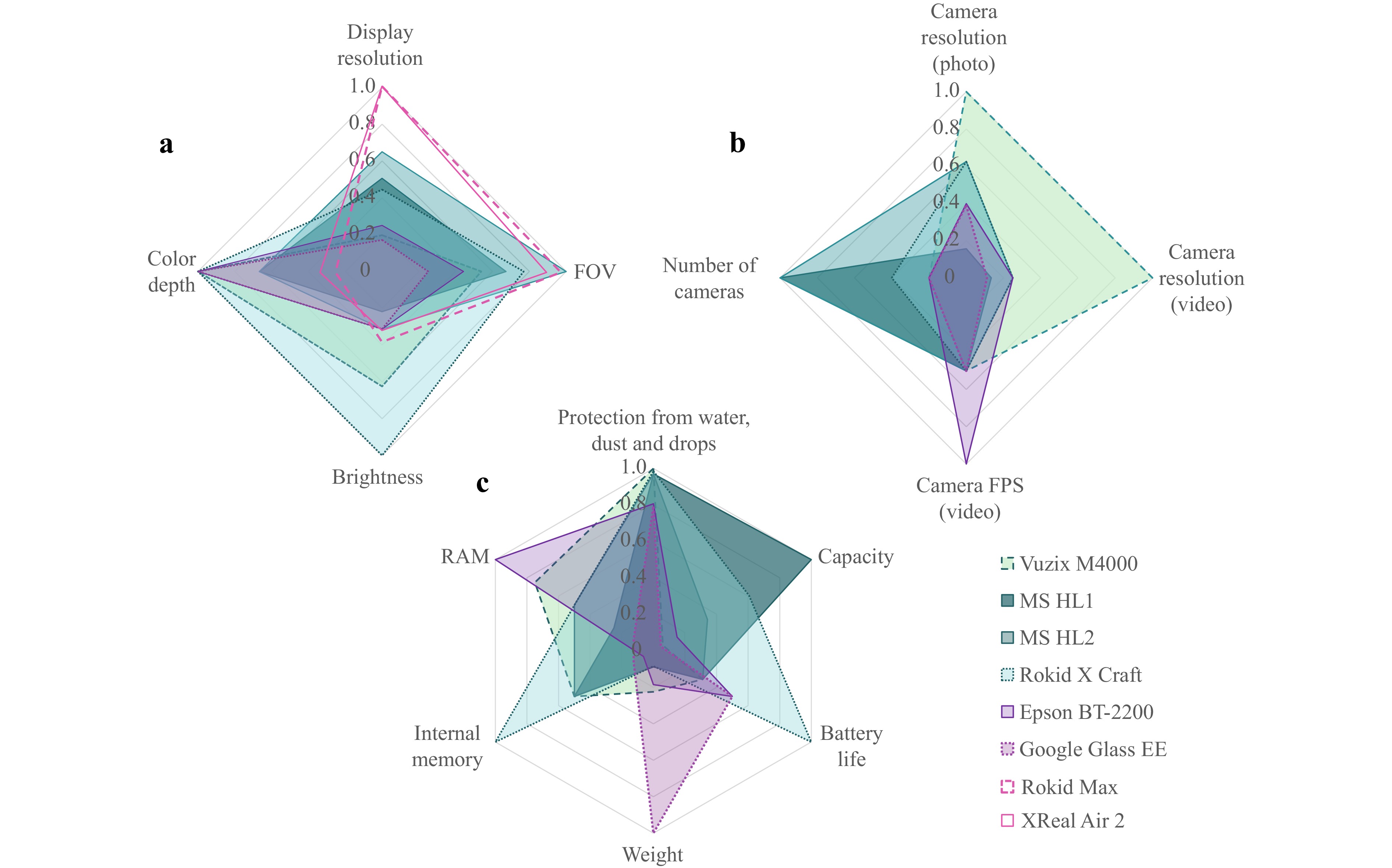
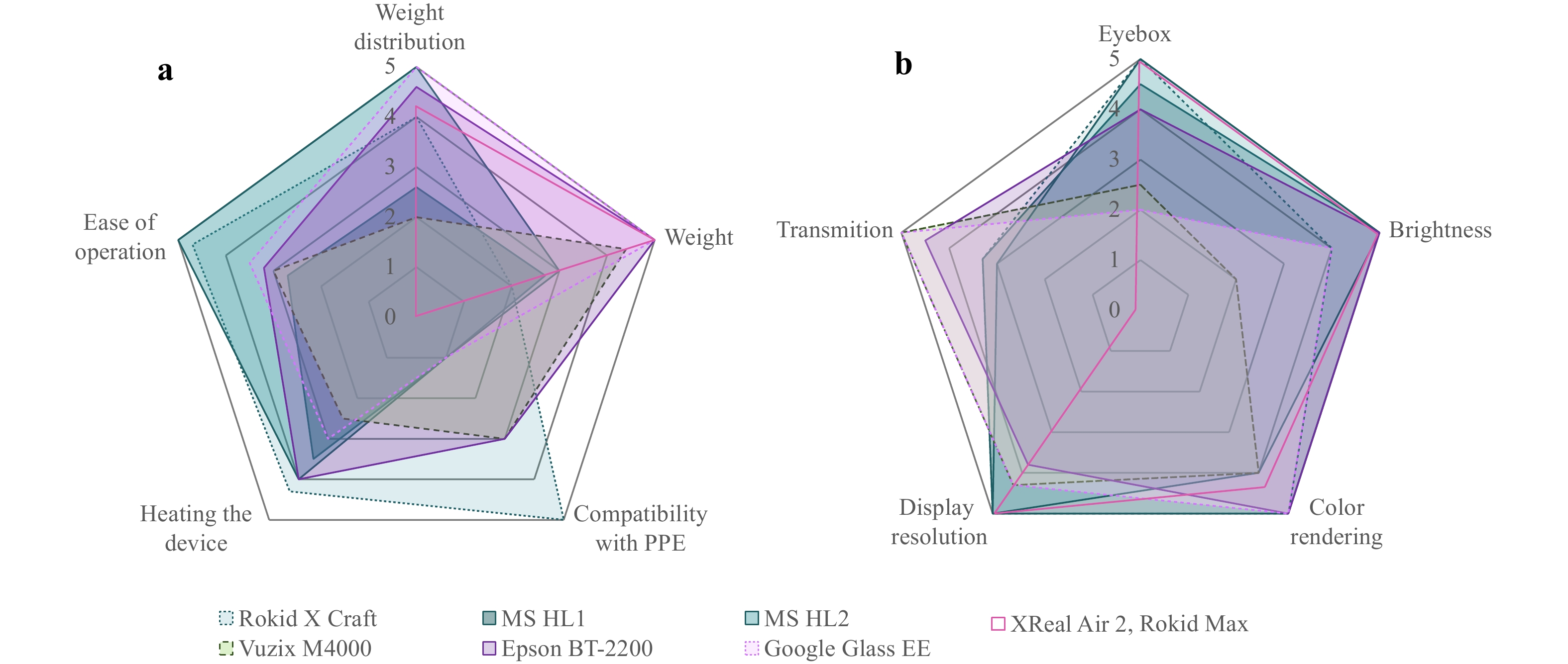
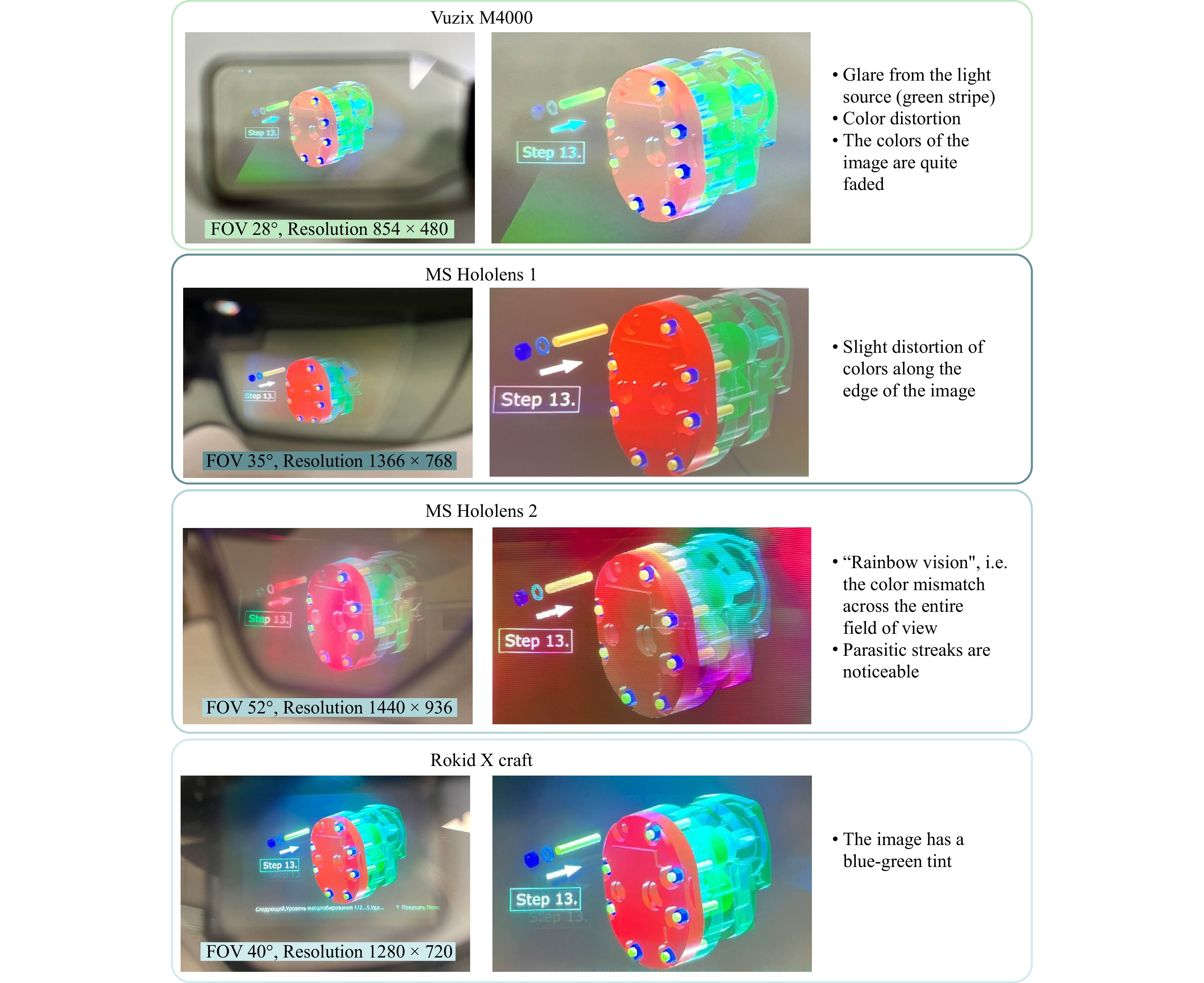
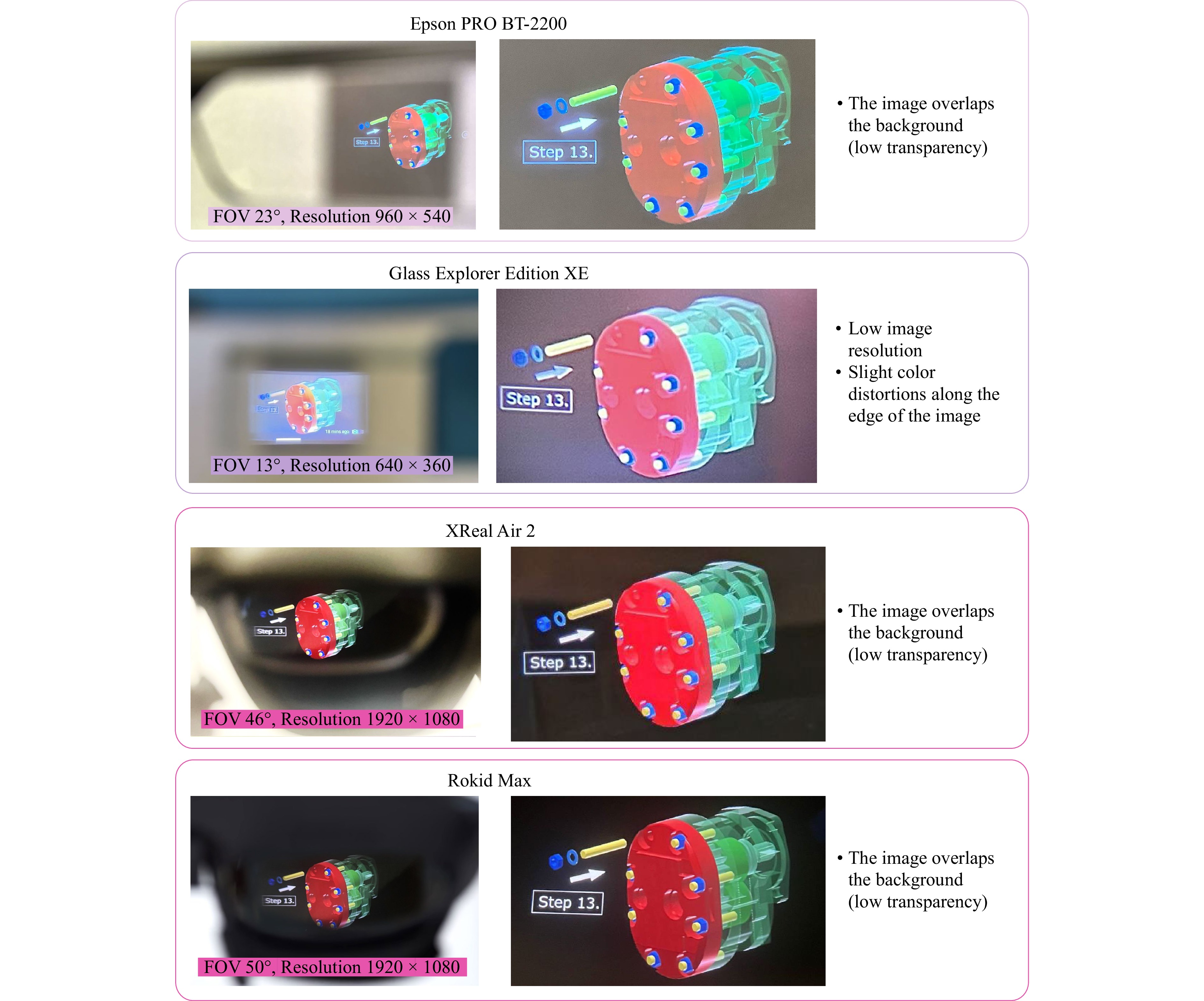
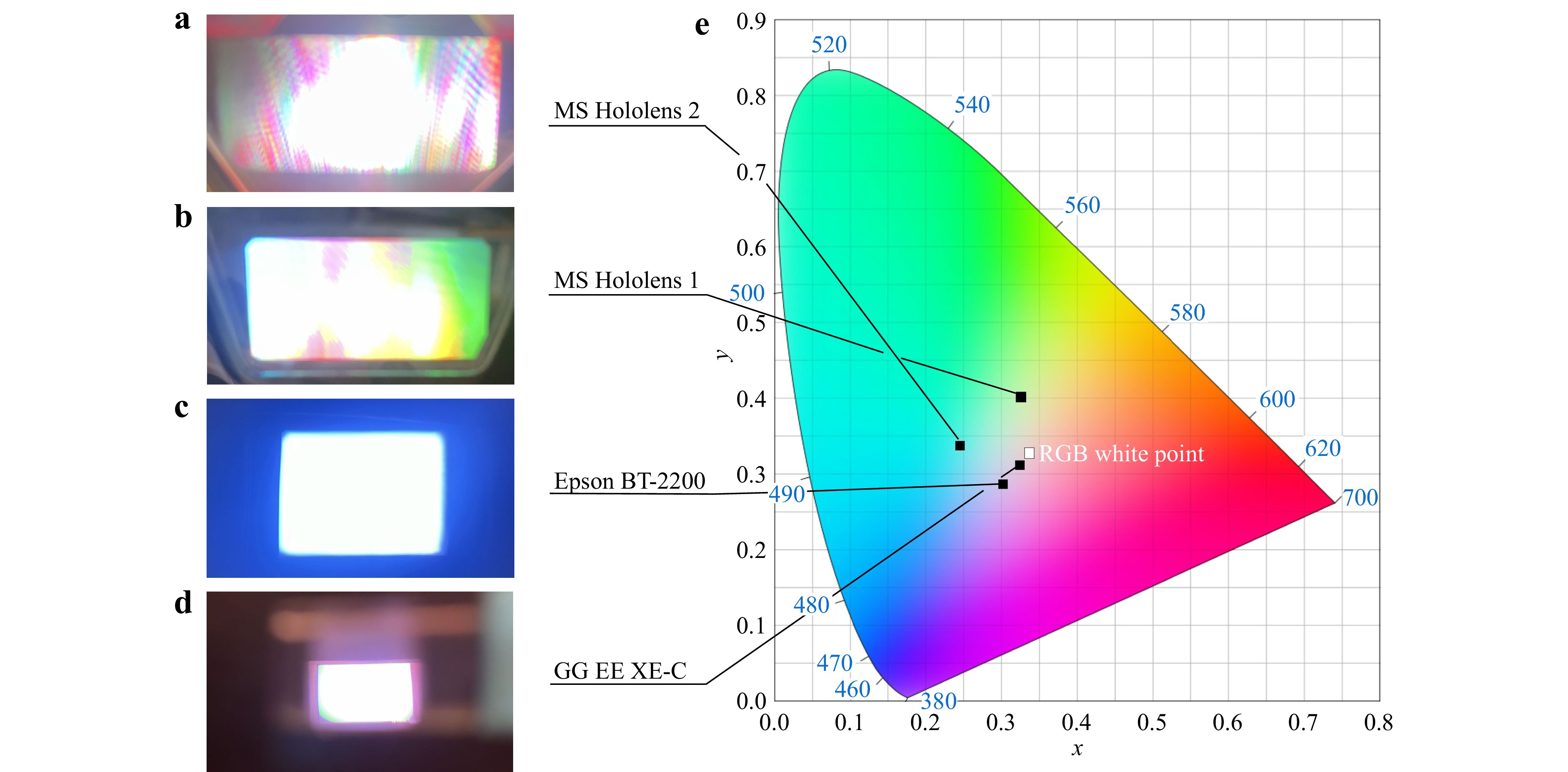
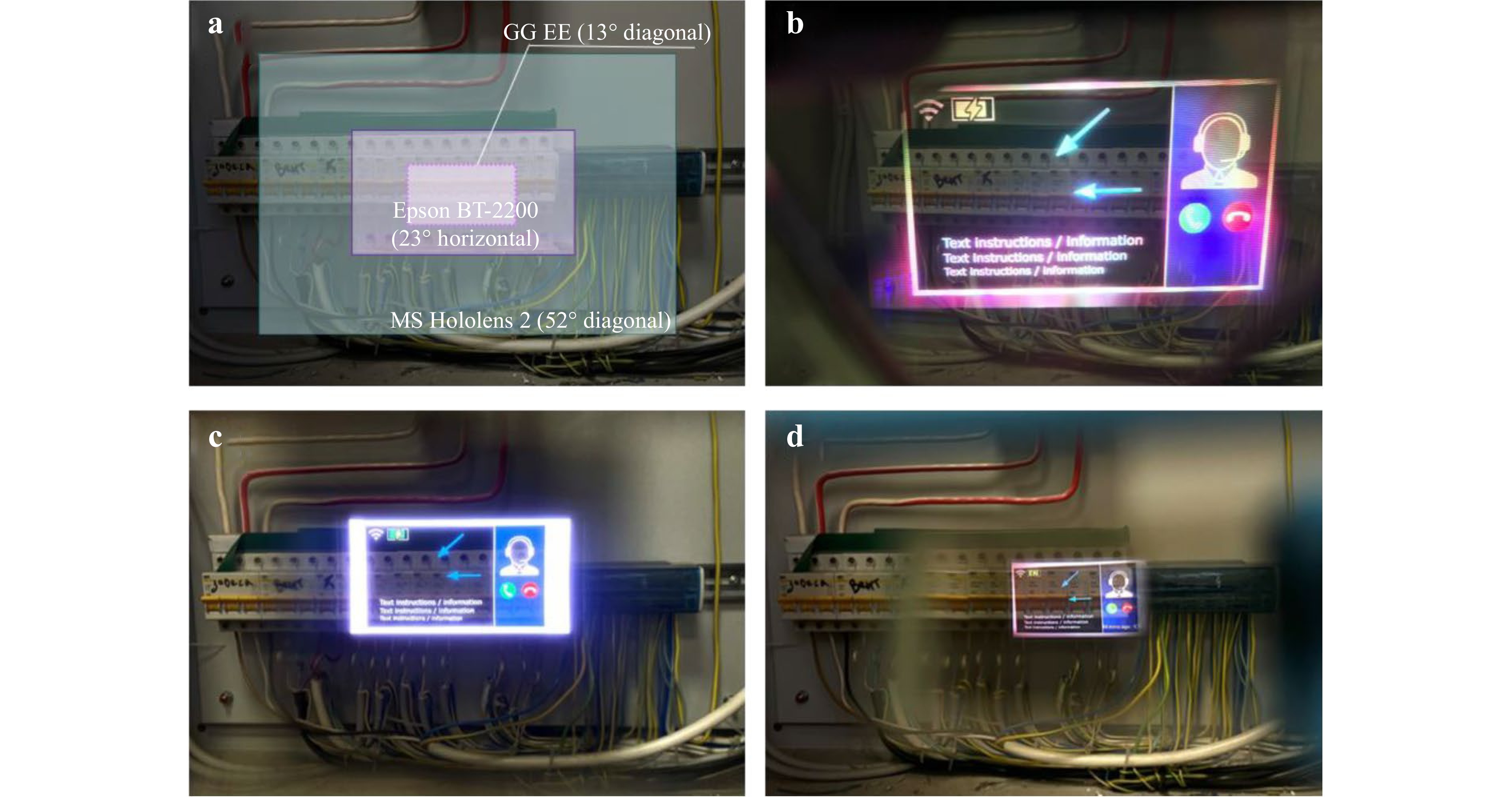
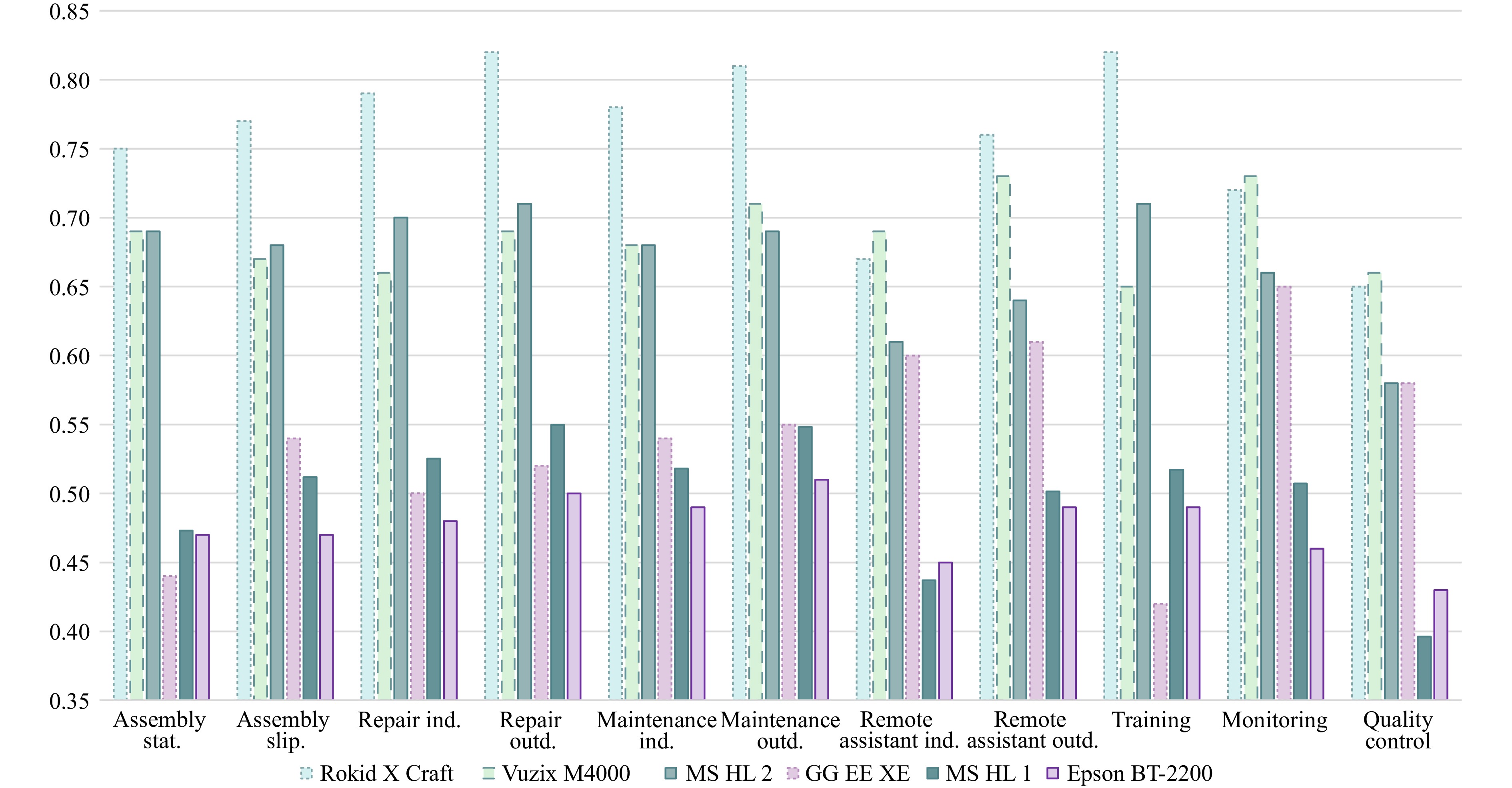
This review considers the modern industrial applications of augmented reality headsets. It draws upon a synthesis of information from open sources and press releases of companies, as well as the first-hand experiences of industry representatives. Furthermore, the research incorporates insights from both profile events and in-depth discussions with skilled professionals. A specific focus is placed on the ergonomic characteristics of headsets: image quality, user-friendliness, etc. To provide an objective evaluation of the various headsets, a metric has been proposed which is dependent on the specific application case. This enables a comprehensive comparison of the various devices in terms of their quantitative characteristics, which is of particular importance for the formation of a rapidly developing industry.
- First
- Prev
- 1
- 2
- 3
- 4
- 5
- 6
- 7
- Next
- Last
- Total:7
- To
- Go


 Email
Email RSS
RSS