
Special Issue | 13 March 2024
Special Issue on a 90-year journey towards light from the intramolecular universe

For nearly 90 years, scientists have unraveled intramolecular motion and chemical bonds, sparked by E. Synge's 1928 breakthrough in optical resolution. Near-field optical microscopy, surpassing classical limits, enables Angstrom-level spatial resolution. With this special issue ‘Nanospectroscopy, nanooptics and nanofabrication’, we wish to highlight the rapid experimental and theoretical advances of this burgeoning interdisciplinary field, as well as to provide an account of its peculiar challenges and future prospects.
This issue is co-edited by
Dr. Dai Zhang, Institute of Physical and Theoretical Chemistry, Eberhard Karls University ofTubingen, Germany
Dr Hai Bi, Jihua Laboratory, P.R. China
-
Article
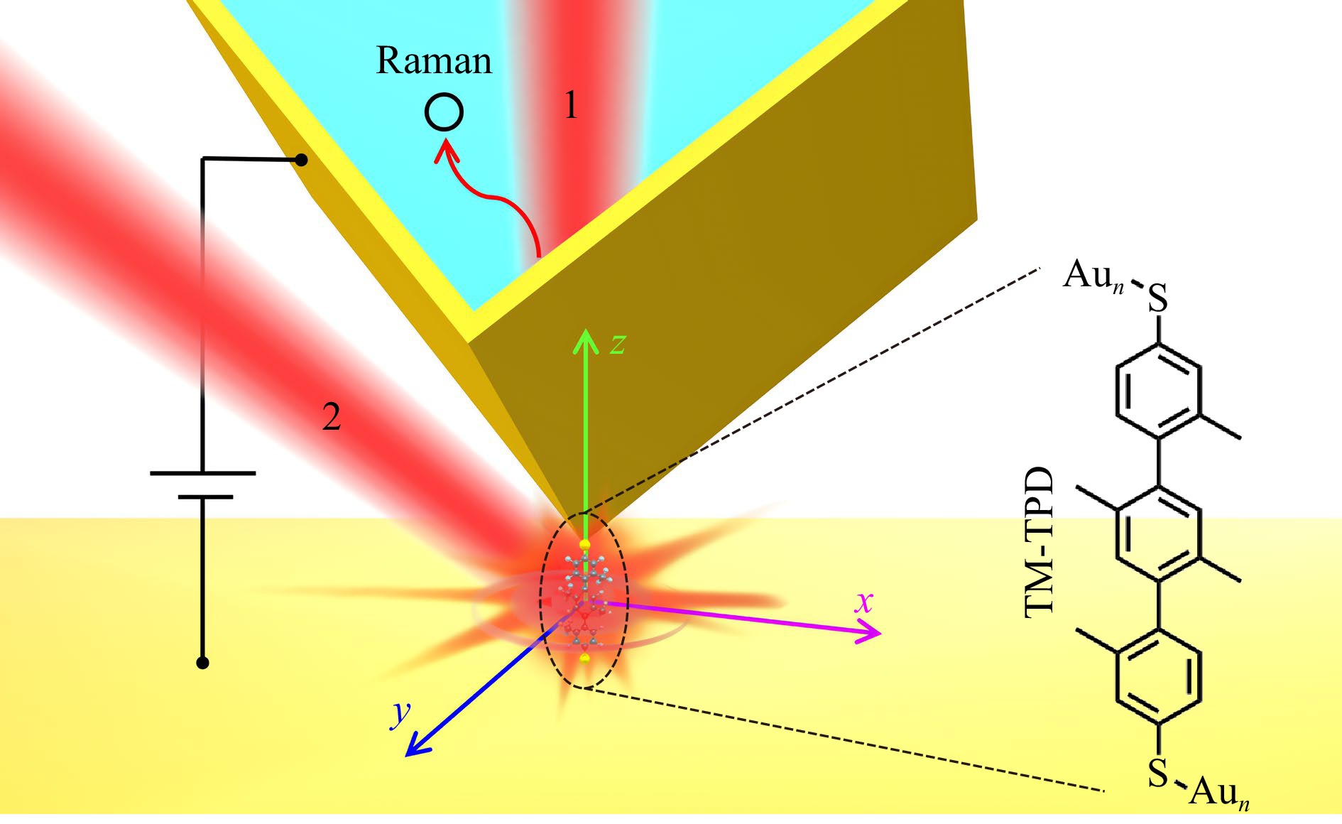
Effect of near-field optical angular momentum on molecular junctions
 Published , Published online: 29 September 2023 , doi: 10.37188/lam.2023.034
The role of molecular junctions in nanoelectronics is most often associated with electronic transport; however, their precise characterisation hinders their widespread development. The interaction of light with molecular junctions is a supplementary factor for the development of molecular switches, but it has rarely been addressed. The influence of light interaction with molecular junctions on the response of molecules in the near field was demonstrated by properly characterising the optical angular momentum at the junctions. Consequently, the molecular switching dynamics were observed in the Raman signatures of the conducting molecules. The illumination geometry and voltage applied to the junction were changed to demonstrate numerically and experimentally how the Raman intensity can be turned ON and OFF with a difference of nearly five orders of magnitude. These molecular-scale operations result from the combined interaction of a current-induced electronic rearrangement in the molecular junction and a plasmonically enhanced electromagnetic field near the tip of the junction. This study of the effect of optical angular momentum on the near field of the molecular junction shows significant potential for the development of molecular electronics.
-
Article
Tip-induced bond weakening, tilting, and hopping of a single CO molecule on Cu(100)
 Published , Published online: 01 December 2022 , doi: 10.37188/lam.2022.052
The interaction between a probing tip and an adsorbed molecule can significantly impact the molecular chemical structure and even induce its motion on the surface. In this study, the tip-induced bond weakening, tilting, and hopping processes of a single molecule were investigated by sub-nanometre resolved tip-enhanced Raman spectroscopy (TERS). We used single carbon monoxide (CO) molecules adsorbed on the Cu (100) surface as a model system for the investigation. The vibrational frequency of the C−O stretching mode is always redshifted as the tip approaches, revealing the weakening of the C−O bond owing to tip−molecule interactions. Further analyses of both the vibrational Stark effect and TERS imaging patterns suggest a delicate tilting phenomenon of the adsorbed CO molecule on Cu(100), which eventually leads to lateral hopping of the molecule. While a tilting orientation is found toward the hollow site along the [110] direction of the Cu(100) surface, the hopping event is more likely to proceed via the bridge site to the nearest Cu neighbour along the [100] or [010] direction. Our results provide deep insights into the microscopic mechanisms of tip−molecule interactions and tip-induced molecular motions on surfaces at the single-bond level.
-
Article
FEM-based modeling of microsphere-enhanced interferometry
 Published , Published online: 28 October 2022 , doi: 10.37188/lam.2022.049
To improve the lateral resolution in microscopic imaging, microspheres are placed close to the object’ s surface in order to support the imaging process by optical near-field information. Although microsphere-assisted measurements are part of various recent studies, no generally accepted explanation for the effect of microspheres exists. Photonic nanojets, enhancement of the numerical aperture, whispering-gallery modes and evanescent waves are usually named reasons in context with microspheres, though none of these effects is proven to be decisive for the resolution enhancement. We present a simulation model of the complete microscopic imaging process of microsphere-enhanced interference microscopy including a rigorous treatment of the light scattering process at the surface of the specimen. The model consideres objective lenses of high numerical aperture providing 3D conical illumination and imaging. The enhanced resolution and magnification by the microsphere is analyzed with respect to the numerical aperture of the objective lenses. Further, we give a criterion for the achievable resolution and demonstrate that a local enhancement of the numerical aperture is the most likely reason for the resolution enhancement.
-
Article
Design and realization of 3D printed fiber-tip microcantilever probes applied to hydrogen sensing
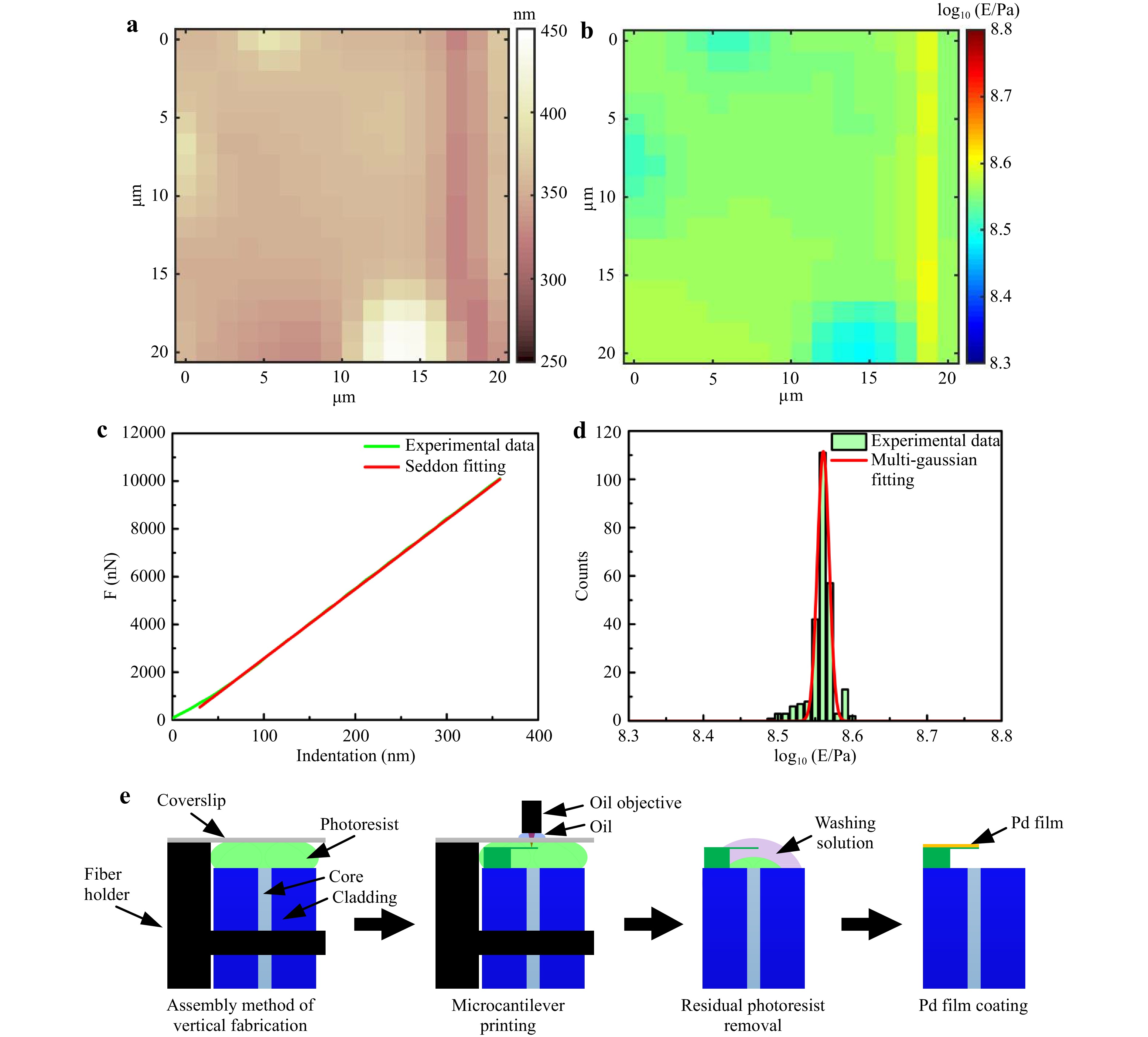 Published , Published online: 24 February 2022 , doi: 10.37188/lam.2022.005Cantilevers in microelectromechanical systems have the advantages of non-labeling, real-time detection, positioning, and specificity. Rectangular solid, rectangular hollow, and triangular microcantilevers were fabricated on an optical fiber tip via two-photon polymerization. The mechanical properties were characterized using finite element simulations. Coating the microcantilever with a palladium film enabled high sensitivity and rapid hydrogen detection. The shape of the cantilever determines the sensitivity, whereas the thickness of the palladium film determines the response time. Additional microelectromechanical systems can be realized via polymerization combined with optical fibers.
 -
Article
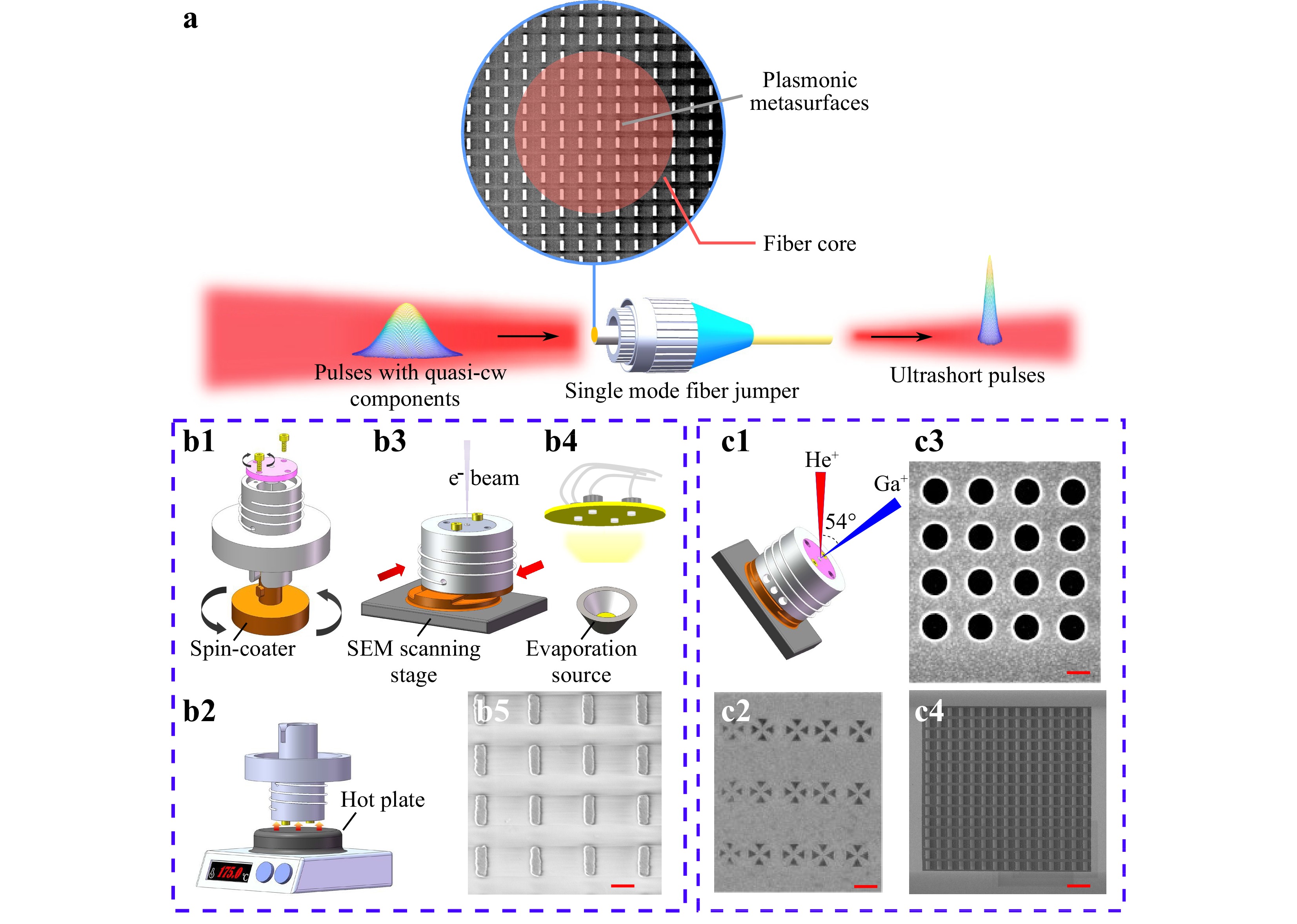
‘Plug-and-play’ plasmonic metafibers for ultrafast fibre lasers
 Published , Published online: 02 September 2022 , doi: 10.37188/lam.2022.045
Metafibers expand the functionalities of conventional optical fibres to unprecedented nanoscale light manipulations by integrating metasurfaces on the fibre tips, becoming an emerging light-coupling platform for both the nanoscience and fibre optics communities. Current metafibers remain proof-of-concept demonstrations that mostly explore isolated bare fibres owing to the lack of standard interfaces with universal fibre networks. Here, we develop methodologies for fabricating well-defined plasmonic metasurfaces directly on the end facets of commercial single -mode fibre jumpers using standard planar technologies and provide the first demonstration of their practical applications in the nonlinear plasmonic regime. Featuring plug-and-play connections with fibre circuitry and arbitrary metasurface landscapes, the metafibers with tunable plasmonic resonances are implemented into fibre laser cavities, yielding all-fibre sub-picosecond (minimum 513 fs) soliton mode locked lasers at optical wavelengths of 1.5 μm and 2 μm, demonstrating their unusual polarimetric nonlinear transfer functions and superior saturation absorption responses. The nanofabrication process flow is compatible with existing cleanroom technologies, offering metafibers an avenue to become a regular member of functionalised fibre components. This work paves the way toward the next generation of ultrafast lasers, optical frequency combs, and ultracompact ‘all-in-fibre’ optical systems.
-
Article
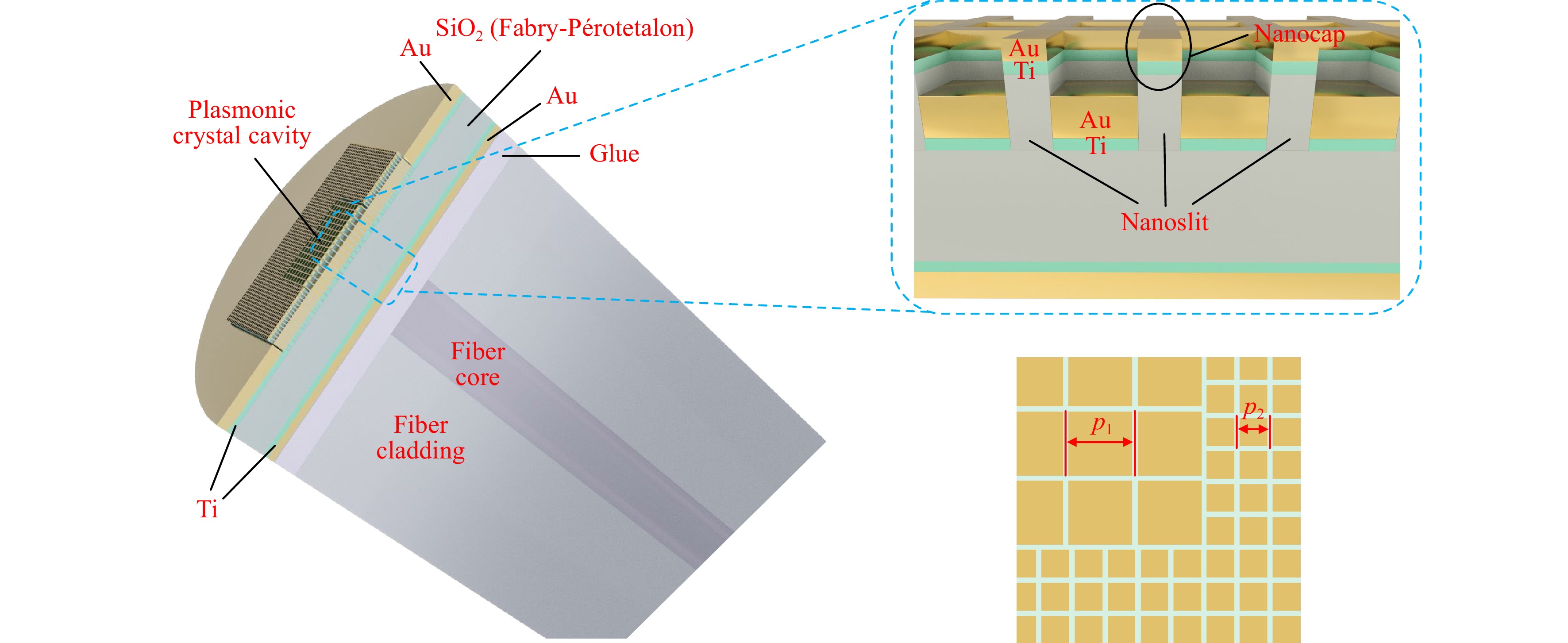
A quasi-3D Fano resonance cavity on optical fiber end-facet for high signal-to-noise ratio dip-and-read surface plasmon sensing
 Published , Published online: 18 September 2022 , doi: 10.37188/lam.2022.046
Surface plasmon devices mounted at the end-facets of optical fibers are appealing candidates for rapid and point-of-care sensing applications, by offering a special dip-and-read operation mode. At present, these devices’ noise-equivalent limits-of-detection lag far behind the free-space counterparts, leaving them incapable of most biosensing applications. Here we report a quasi-3D Fano resonance cavity and its fabrication method to fundamentally improve the quality factor and coupling efficiency for fiber-coupled surface plasmon resonance. In this device, the Fano resonance combines the high coupling efficiency of a Fabry-Pérot etalon and the high quality factor resonance of a plasmonic crystal cavity. The quasi-3D device was fabricated on a planar substrate and transferred to a single-mode fiber end-facet, which requires a low-adhesion yet surface-plasmon-tunneling interface between the device and the planar substrate. Such an interface was realized with a nanocap-slit unit structure, of which the plasmonic crystal was consisted. A noise-equivalent limit of detection of ~ 10-7 RIU was experimentally obtained, allowing bovine serum albumin physical adsorption to be distinguished at ng mL-1 level concentrations. Therefore, breaking through the long-standing signal-to-noise ratio bottleneck, this work makes fiber end-facet surface plasmon devices into one of high sensitivity label-free sensing technologies. At the same time, it provides an enabling top-down fabrication technology for making 3D plasmonic structures on fiber end-facets at the nanometer scale.
-
Article
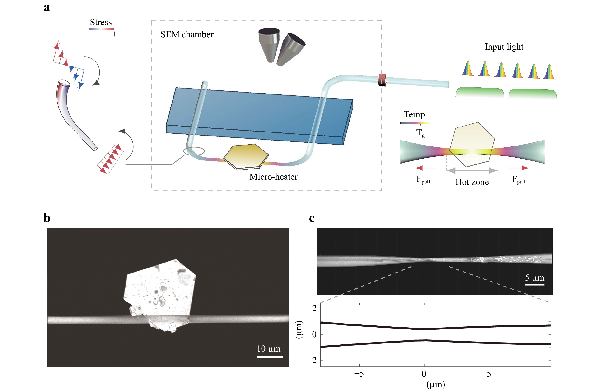
Fibre tapering using plasmonic microheaters and deformation-induced pull
 Published , Published online: 23 March 2023 , doi: 10.37188/lam.2023.005
Optical fibres with diameters at micro- or sub-micrometre scale are widely adopted as a convenient tool for studying light–matter interactions. To prepare such devices, two elements are indispensable: a heat source and a pulling force. In this paper, we report a novel fibre-tapering technique in which micro-sized plasmonic heaters and elaborately deformed optical fibres are compactly combined, free of flame and bulky pulling elements. Using this technique, micro-nano fibres with abrupt taper and ultra-short transition regions were successfully fabricated, which would otherwise be a challenge for traditional techniques. The compactness of the proposed system enabled it to be further transferred to a scanning electron microscope for in-situ monitoring of the tapering process. The essential dynamics of “heat and pull” was directly visualised with nanometre precision in real time and theoretically interpreted, thereby establishing an example for future in-situ observations of micro and nanoscale light-matter interactions.
-
Article
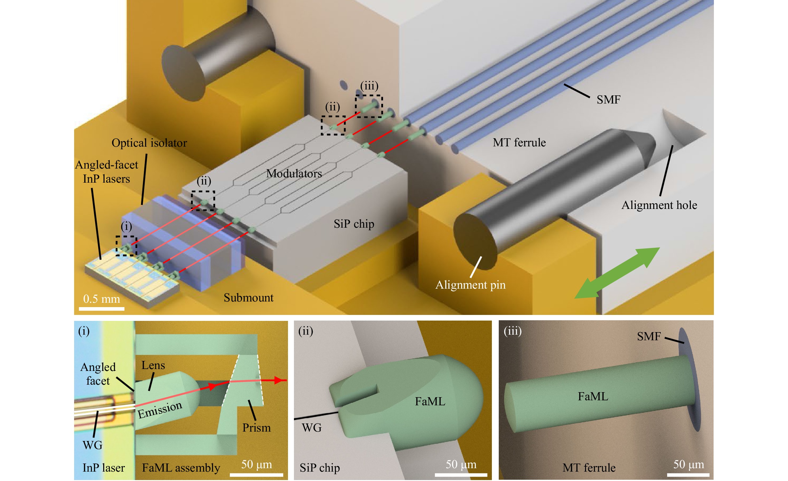
3D-printed facet-attached microlenses for advanced photonic system assembly
 Published , Published online: 17 April 2023 , doi: 10.37188/lam.2023.003
Wafer-level mass production of photonic integrated circuits (PIC) has become a technological mainstay in the field of optics and photonics, enabling many novel and disrupting a wide range of existing applications. However, scalable photonic packaging and system assembly still represents a major challenge that often hinders commercial adoption of PIC-based solutions. Specifically, chip-to-chip and fiber-to-chip connections often rely on so-called active alignment techniques, where the coupling efficiency is continuously measured and optimized during the assembly process. This unavoidably leads to technically complex assembly processes and high cost, thereby eliminating most of the inherent scalability advantages of PIC-based solutions. In this paper, we demonstrate that 3D-printed facet-attached microlenses (FaML) can overcome this problem by opening an attractive path towards highly scalable photonic system assembly, relying entirely on passive assembly techniques based on industry-standard machine vision and/or simple mechanical stops. FaML can be printed with high precision to the facets of optical components using multi-photon lithography, thereby offering the possibility to shape the emitted beams by freely designed refractive or reflective surfaces. Specifically, the emitted beams can be collimated to a comparatively large diameter that is independent of the device-specific mode fields, thereby relaxing both axial and lateral alignment tolerances. Moreover, the FaML concept allows to insert discrete optical elements such as optical isolators into the free-space beam paths between PIC facets. We show the viability and the versatility of the scheme in a series of selected experiments of high technical relevance, comprising pluggable fiber-chip interfaces, the combination of PIC with discrete micro-optical elements such as polarization beam splitters, as well as coupling with ultra-low back-reflection based on non-planar beam paths that only comprise tilted optical surfaces. Based on our results, we believe that the FaML concept opens an attractive path towards novel PIC-based system architectures that combine the distinct advantages of different photonic integration platforms.
-
Review
Photopatterning via photofluidization of azobenzene polymers
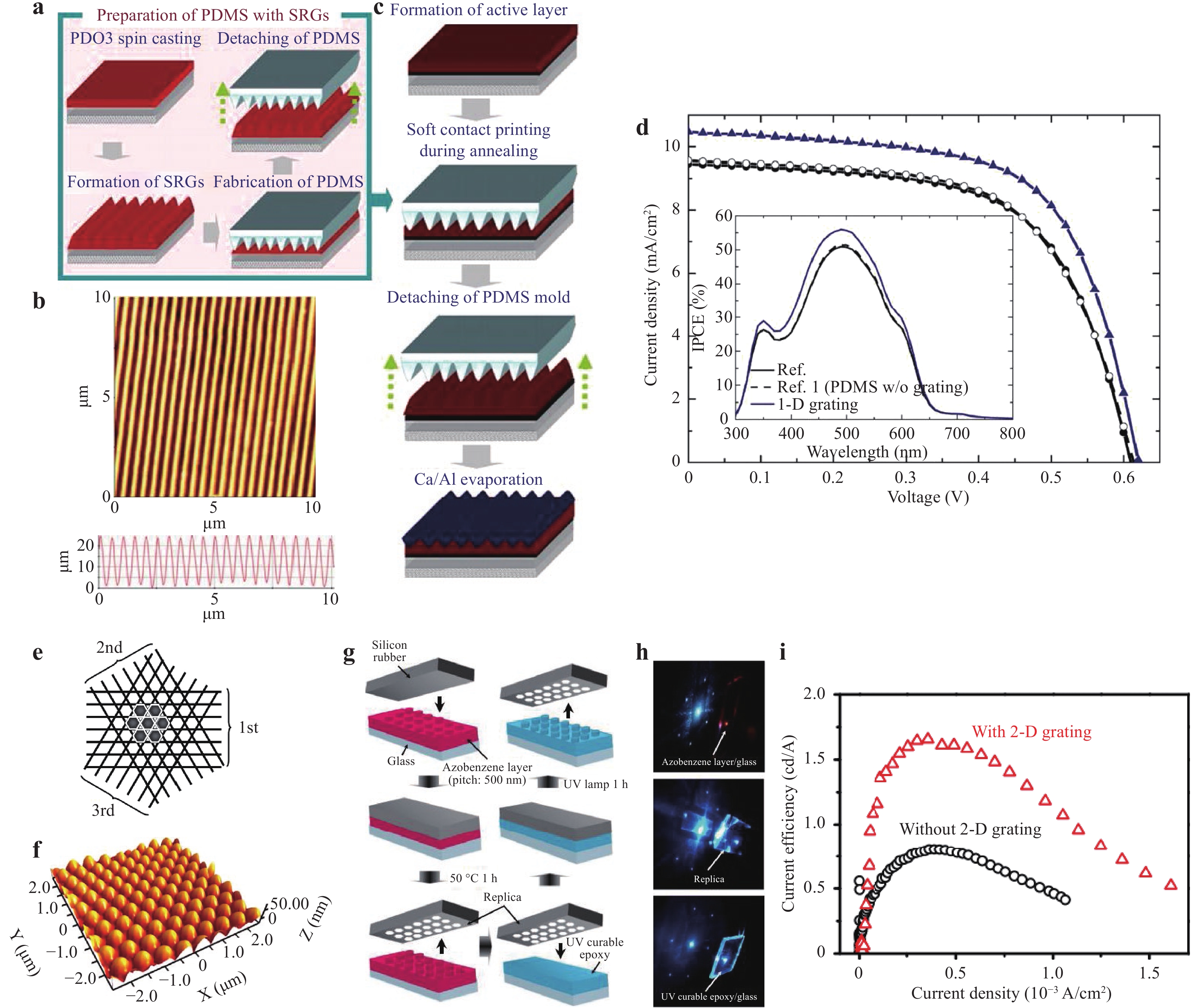 Published , Published online: 26 January 2022 , doi: 10.37188/lam.2022.003In current photo-based patterning techniques, an image is projected onto a photosensitive material to generate a pattern in the area where the light is focused. Thus, the size, shape, and periodicity of the pattern are determined by the features on the photomask or projected images, and the materials themselves generally do not play an active role in changing the features. In contrast, azobenzene polymers offer a unique type of photopatterning platform, where photoisomerization of the azobenzene groups can induce substantial material movements at the molecular, micro-, and macroscales. Stable surface relief patterns can be generated by exposure to interference light beams. Thus, periodic nano- and microstructures can be fabricated with both two- and three-dimensional spatial control over a large area in a remarkably simple way. Polarized light can be used to guide the flow of solid azobenzene polymers along the direction of light polarization via an unusual solid-to-liquid transition, allowing for the fabrication of complex structures using light. This review summarizes the recent progress in advanced manufacturing using azobenzene polymers. This includes a brief introduction of the intriguing optical behaviors of azobenzene polymers, followed by discussions of the recent developments and successful applications of azobenzene polymers, especially in micro- and nanofabrication.
 -
Review
Multifaceted Approaches to Engineer Fluorescence in Nanomaterials via a Focused Laser Beam
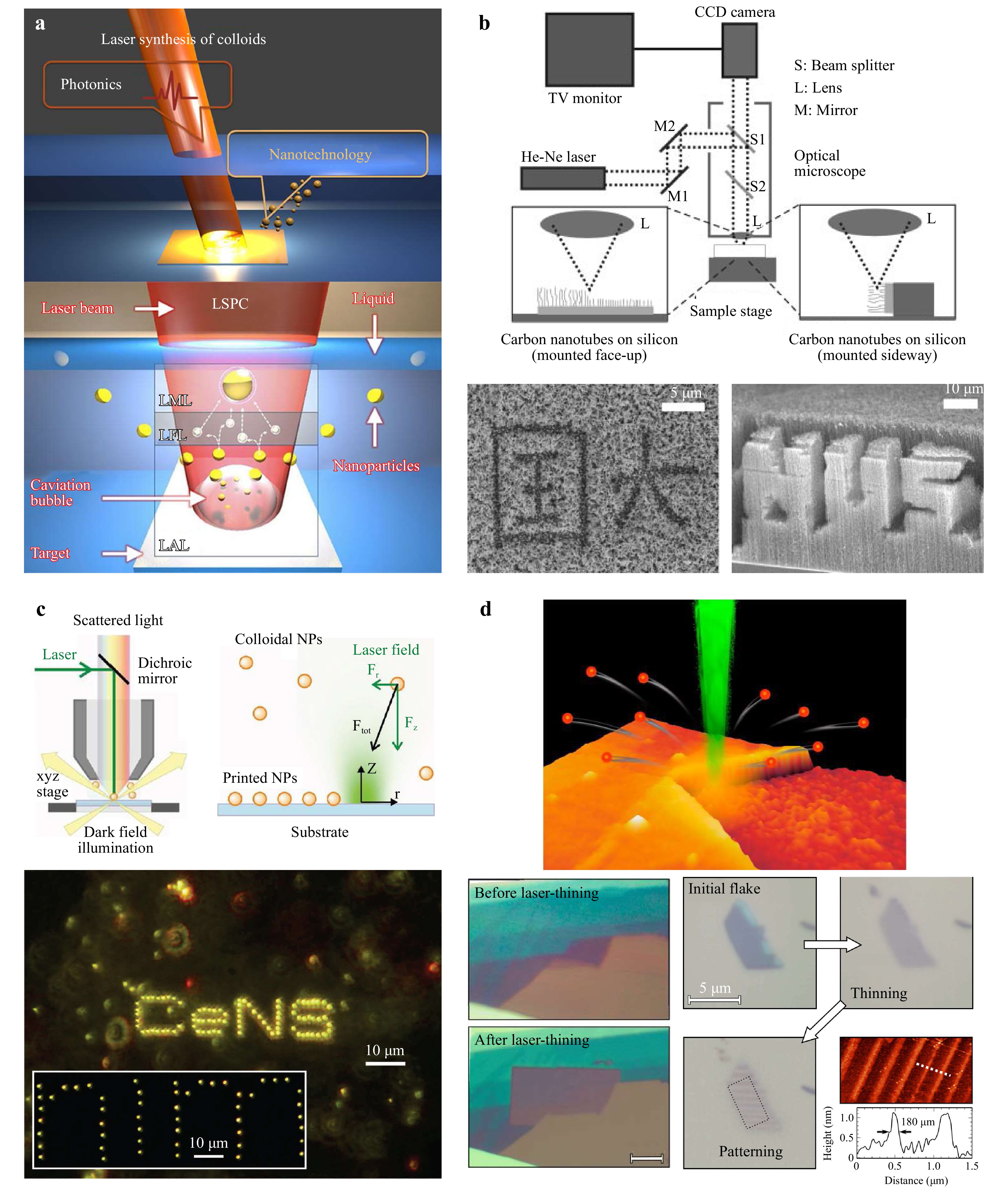 Published , Published online: 14 March 2022 , doi: 10.37188/lam.2022.004Fluorescent nanomaterials have long been recognized as essential contributors to the advancement of material technologies. Over the years, the rapid expansion in this massive selection of materials has led to the emergence of systems with tunable and unique fluorescent properties, occupying pivotal roles across niche areas in imaging, photonics, micro-encryption, and steganographic applications. In recent years, research interest in the translation of laser-based operations towards the production and modulation of nanomaterial fluorescence has been reignited, owing to its ease of operation and low cost. In this paper, we summarize the assortment of laser operations for the fabrication, modification, and spatial positioning of various fluorescent nanomaterials, ranging from metallic nanoparticles, carbon dots, 2D ultrathin films to wide-bandgap nanomaterials, and upconversion nanocrystals. In addition, we evaluate the importance of laser-modified fluorescence for various applications and offer our perspective on the role of laser-based techniques in the forthcoming advancement of nanomaterials.
 -
Article
Two-photon photopolymerization directly initiated by spiropyran photochromic molecules
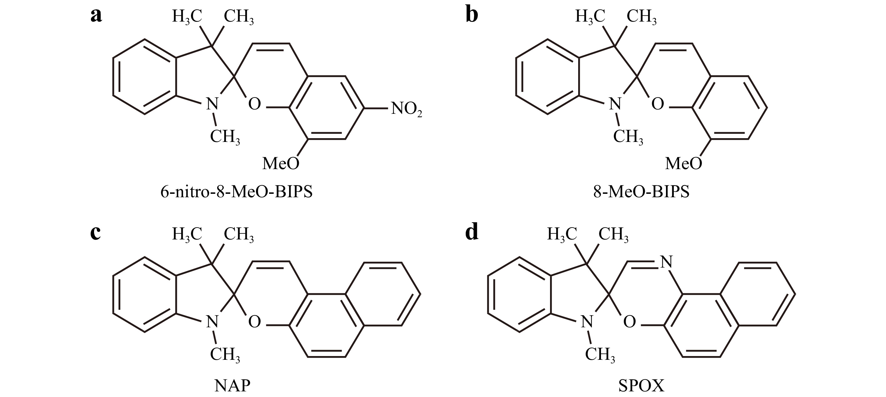 Published , Published online: 24 March 2023 , doi: 10.37188/lam.2023.004
Here, we report the ability of spiropyrans to initiate two-photon polymerization (TPP) for the first time in the literature. The comparison and synergies between the spiropyran photochromic molecule of interest, namely 6-nitro-BIPS, and well-known photoinitiators of radical photopolymerization have been studied. The spiropyran (SPy) molecule can initiate TPP in the presence of trifunctional acrylic monomers and create true 3D structures. The comparison with Irgacure 819, a well-known Type-I photoinitiator, shows that SPy has a comparable capability for TPP. In addition, the combination of SPy with methyl diethanolamine increased the reactivity of both one- and two-photon polymerizations. In the last section, we discuss which SPy isomer is the active photochromic species capable of generating radicals for initiating two-photon polymerization.
-
Article
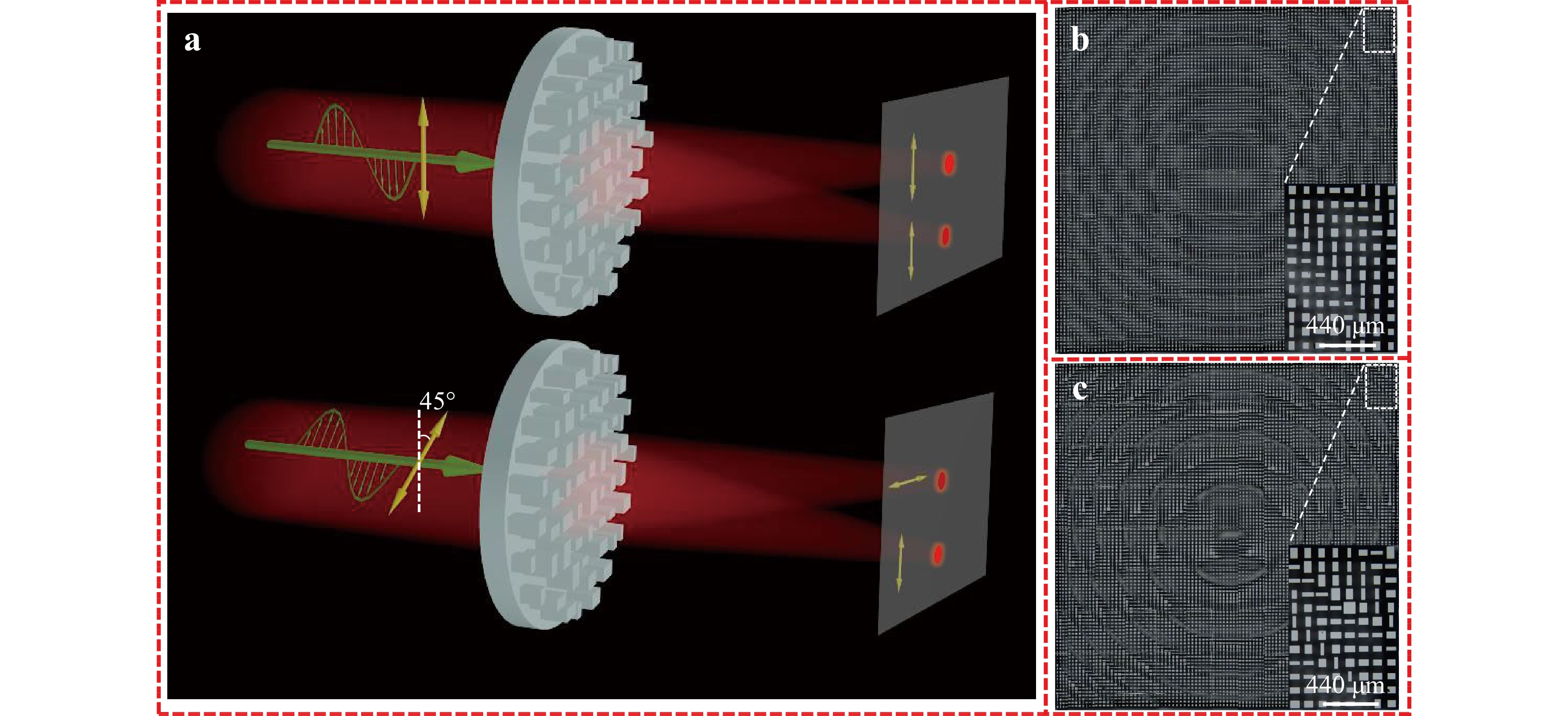
Metasurfaces designed by a bidirectional deep neural network and iterative algorithm for generating quantitative field distributions
 Published , Published online: 28 March 2023 , doi: 10.37188/lam.2023.009
Metasurfaces, which are the two-dimensional counterparts of metamaterials, have demonstrated unprecedented capabilities to manipulate the wavefront of electromagnetic waves in a single flat device. Despite various advances in this field, the unique functionalities achieved by metasurfaces have come at the cost of the structural complexity, resulting in a time-consuming parameter sweep for the conventional metasurface design. Although artificial neural networks provide a flexible platform for significantly improving the design process, the current metasurface designs are restricted to generating qualitative field distributions. In this study, we demonstrate that by combining a tandem neural network and an iterative algorithm, the previous restriction of the design of metasurfaces can be overcome with quantitative field distributions. As proof-of-principle examples, metalenses predicted via the designed network architecture that possess multiple focal points with identical/orthogonal polarisation states, as well as accurate intensity ratios (quantitative field distributions), were numerically calculated and experimentally demonstrated. The unique and robust approach for the metasurface design will enable the acceleration of the development of devices with high-accuracy functionalities, which can be applied in imaging, detecting, and sensing.

Dr. Dai Zhang is a research group leader at the Eberhard Karl’s University of Tübingen, Germany. Her research interests lie in the field of high-resolution optical microscopy and spectroscopy and their applications in semiconductor materials. She has authored or co-authored more than 100 refereed journal papers with over 3000 citations, and has delivered over 50 invited talks at international and national conferences. She was awarded Annual Prize for exceptional young scientists from the Work Association of German University Professors for Chemistry; and the Helene-Lange-Prize for outstanding young female scientists for their exceptional work in research and teaching, Germany.

Dr. Hai Bi is the principle investigator and the founder of the Germany-China Joint Innovation Laboratory at Ji Hua Laboratory. He completed his B.S. and M.S. degree in Chemistry at Jilin University in 2007 and 2010, respectively, and received his doctoral degree in Physics from Technique University of Munich in 2014. Afterwards, he worked as a research associate at Harvard University (2015-2019). In 2020, he started his work at Ji Hua Laboratory. His research focuses on super-resolution microscopy with near-field enhanced mechanism, organic semiconductors and optoelectronic devices. He is devoted to developing methods and technologies for practical industrial fields, especially for OLED technique.

 Email
Email RSS
RSS