
View by Category
Published
, Published online: 29 July 2026
, doi: 10.37188/lam.2026.022
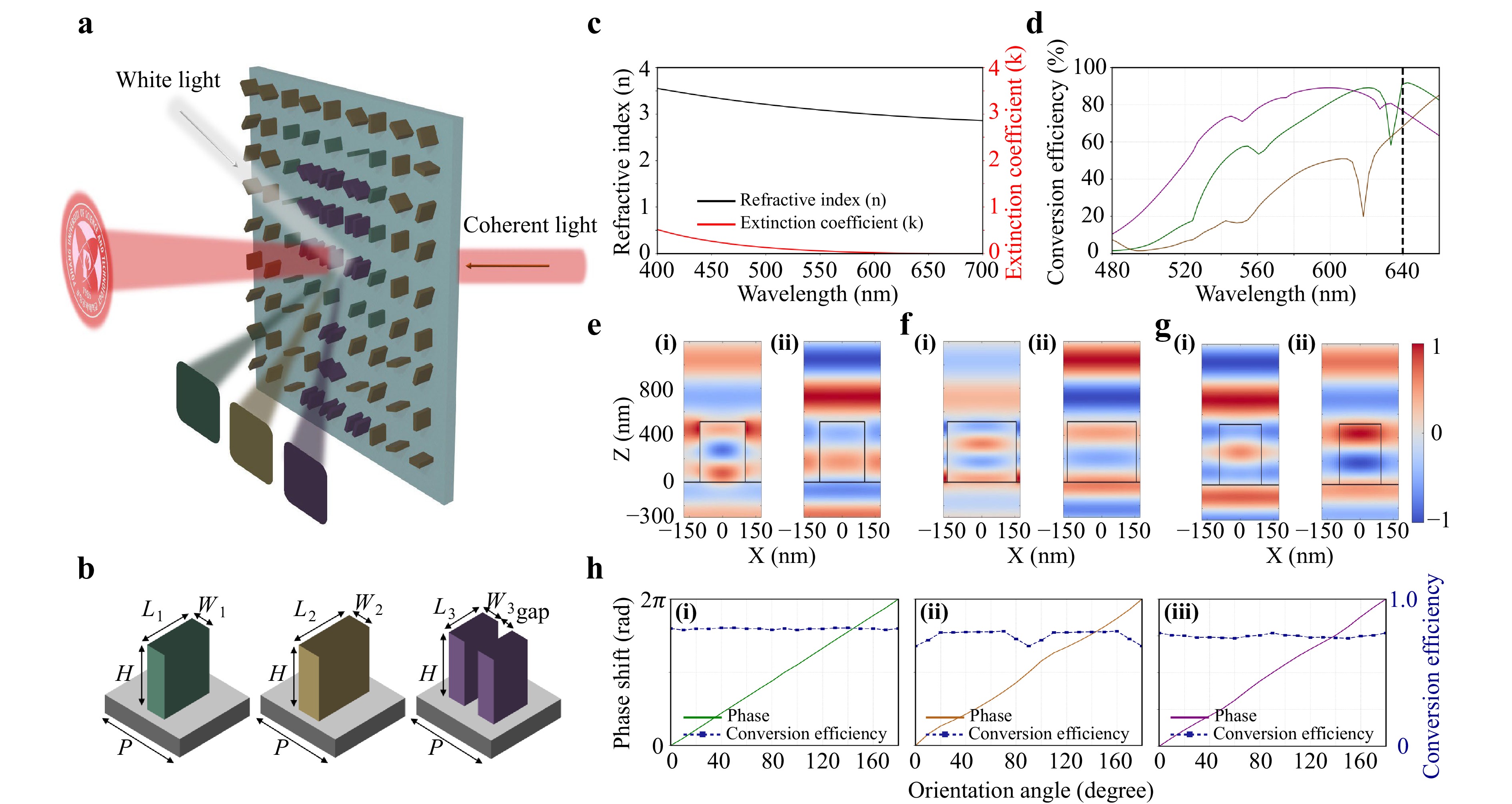
Metasurfaces, flat optical devices built from nanoscale structures, offer powerful and precise control over light. They have enabled applications such as structural color printing by manipulating spectral responses and holography through precise phase control. Integrating these functions into a single metasurface has gained interest for compact multifunctional platforms. However, most existing dual-mode designs suffer from low hologram efficiency, limiting their practical applications in multifunctional optical systems. Here, we present dual-functional metasurfaces that simultaneously enable three-color structural printing under white light illumination and high-efficiency holography under coherent light. Our design employs three distinct meta-atoms, composed of single and double nanorods, to achieve independent spectral and phase modulations. The metasurfaces produce three distinct reflective colors of green, brown, and magenta and achieve numerical conversion efficiency up to 90% at the 640 nm wavelength. The fabricated devices successfully display desired structural colors under white light and reconstruct holographic images with high efficiency under coherent illumination. The devices also demonstrate broadband performance for holography across the visible spectrum. These results confirm the effectiveness of our design in achieving independent and efficient control of color and holography within a single metasurface. This multifunctional capability offers strong potential for applications in anti-counterfeiting and compact optical data storage.


Published
, Published online: 17 April 2026
, doi: 10.37188/lam.2026.040
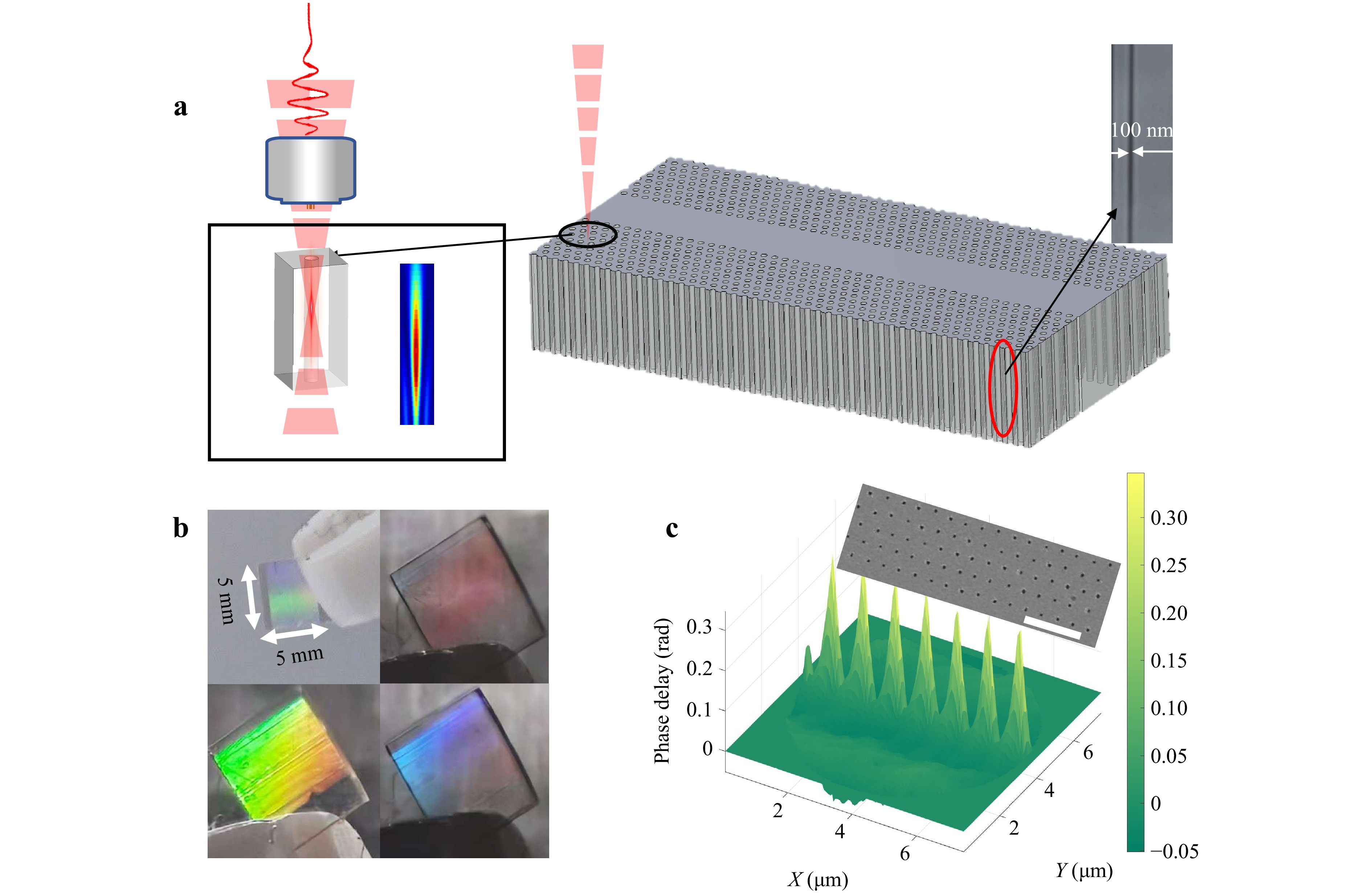
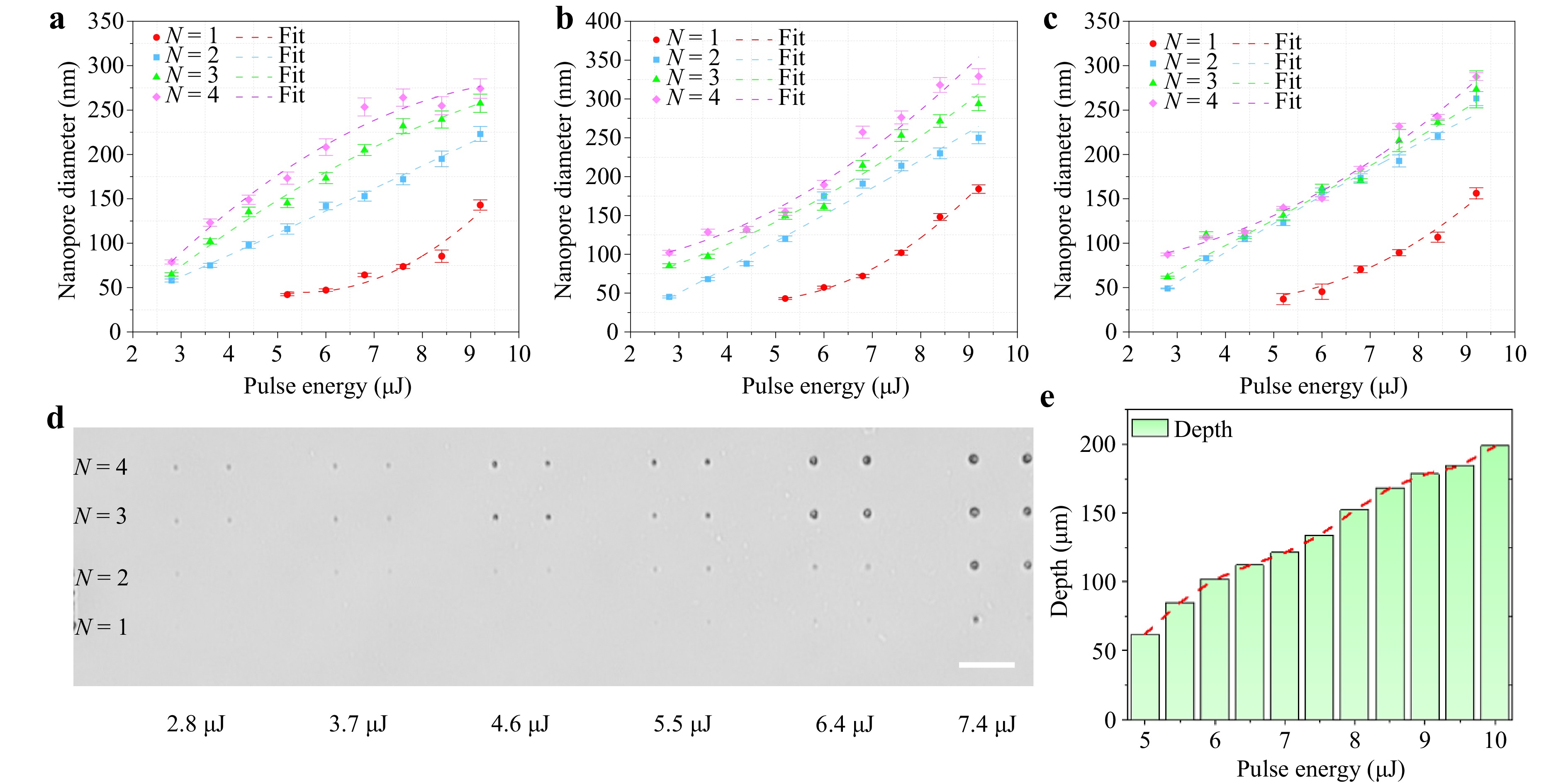
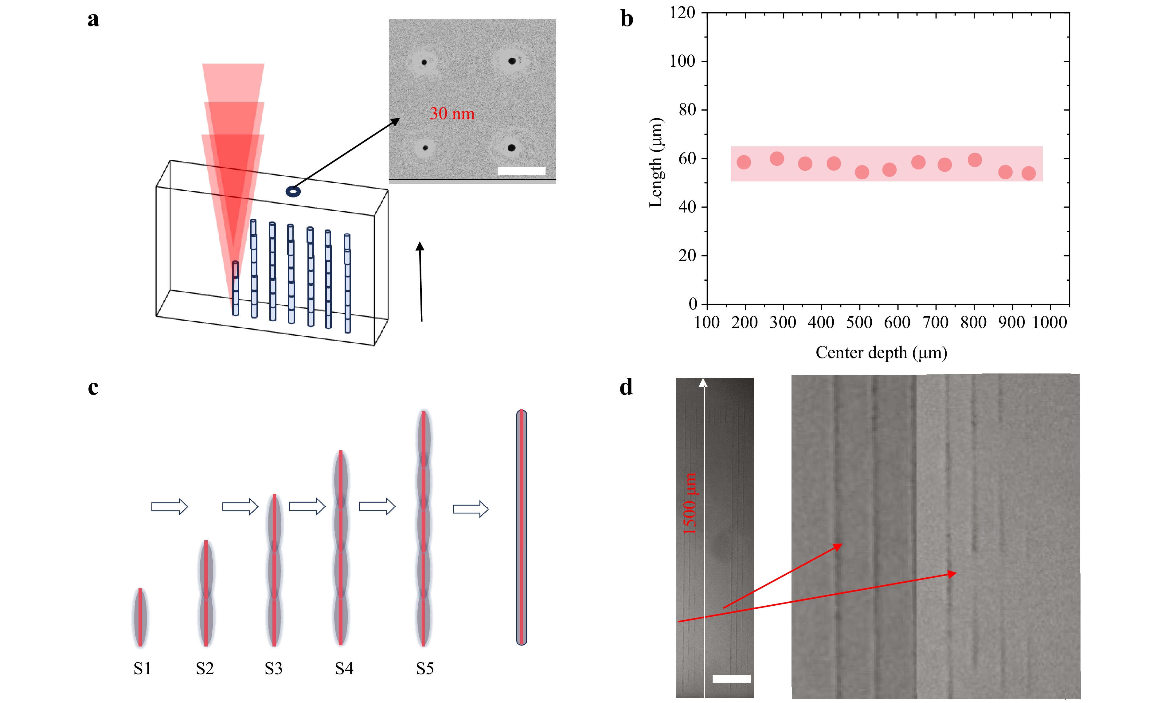
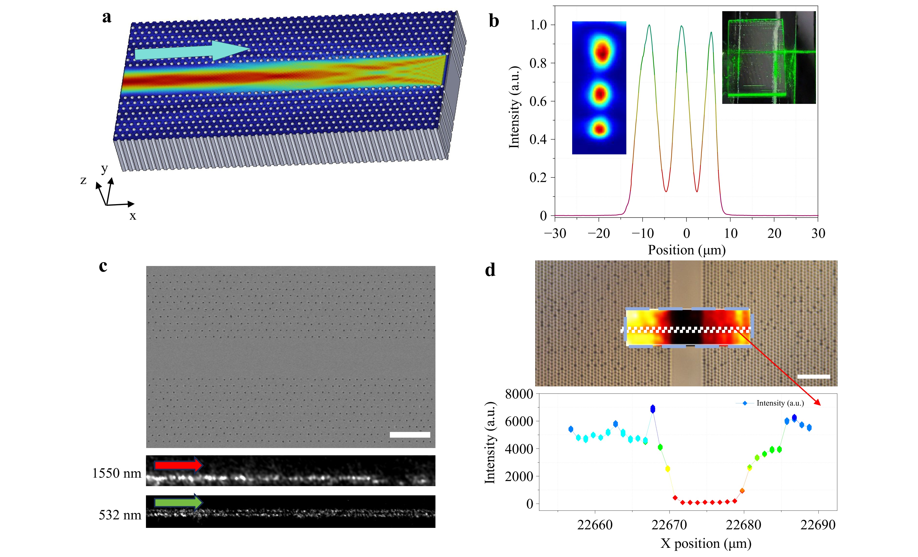
Femtosecond laser writing offers exceptional flexibility and spatial selectivity, enabling the customization of multifunctional integrated devices with nano-scale resolution. This study introduces a novel approach for fabricating nanohole-clad waveguides with ultra-high depth-to-diameter ratios using femtosecond laser writing combined with spherical-aberration-enhanced focal stretching and selective wet etching. This technique not only achieves record depth-to-diameter ratios (>50 000:1) with nanoholes (diameter: 30-500 nm, depth: 1 500 μm) but enables the creation of functional photonic waveguides. The integration of nanoholes into the waveguide structure provides a platform for multi-functional integrated devices, demonstrating significant tunable optical properties. By adjusting pulse energy and axial focal stitching, the diameter of the nanoholes can be tuned from 30 nm to 500 nm with high precision. Further, fluorescent probes embedded within the nanoholes provide a demonstration of optical sensing capabilities, as the waveguide effectively guides light to excite the probes, generating strong detectable signals. The submicron precision achieved through the process ensures high-quality waveguiding with 10.9 dB mode purity, while centimeter-scale periodic arrays exhibit excellent phase uniformity (deviation <3.9%). This work demonstrates the potential of femtosecond laser writing to directly fabricate high-aspect-ratio nanostructures and integrate functional photonic devices on substrates, opening up new possibilities for multi-functional photonics and sensor applications.
Published
, Published online: 15 April 2026
, doi: 10.37188/lam.2026.026
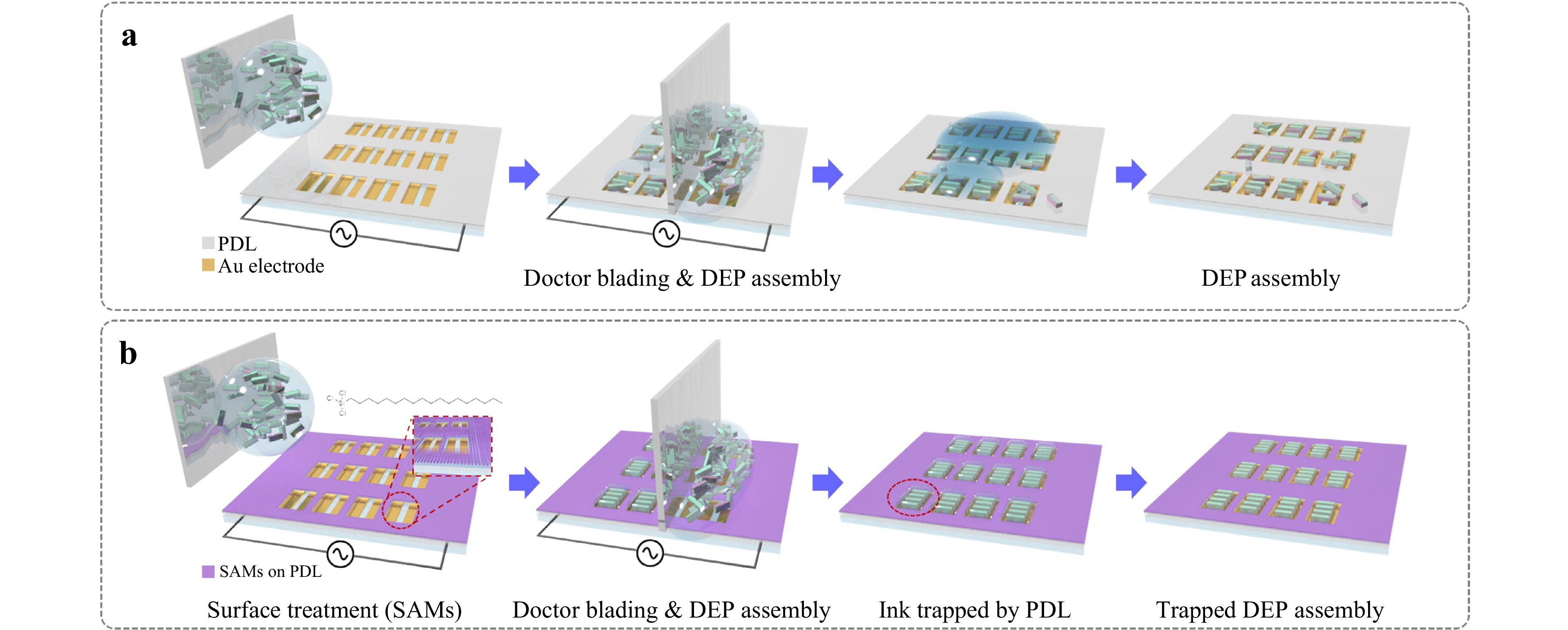
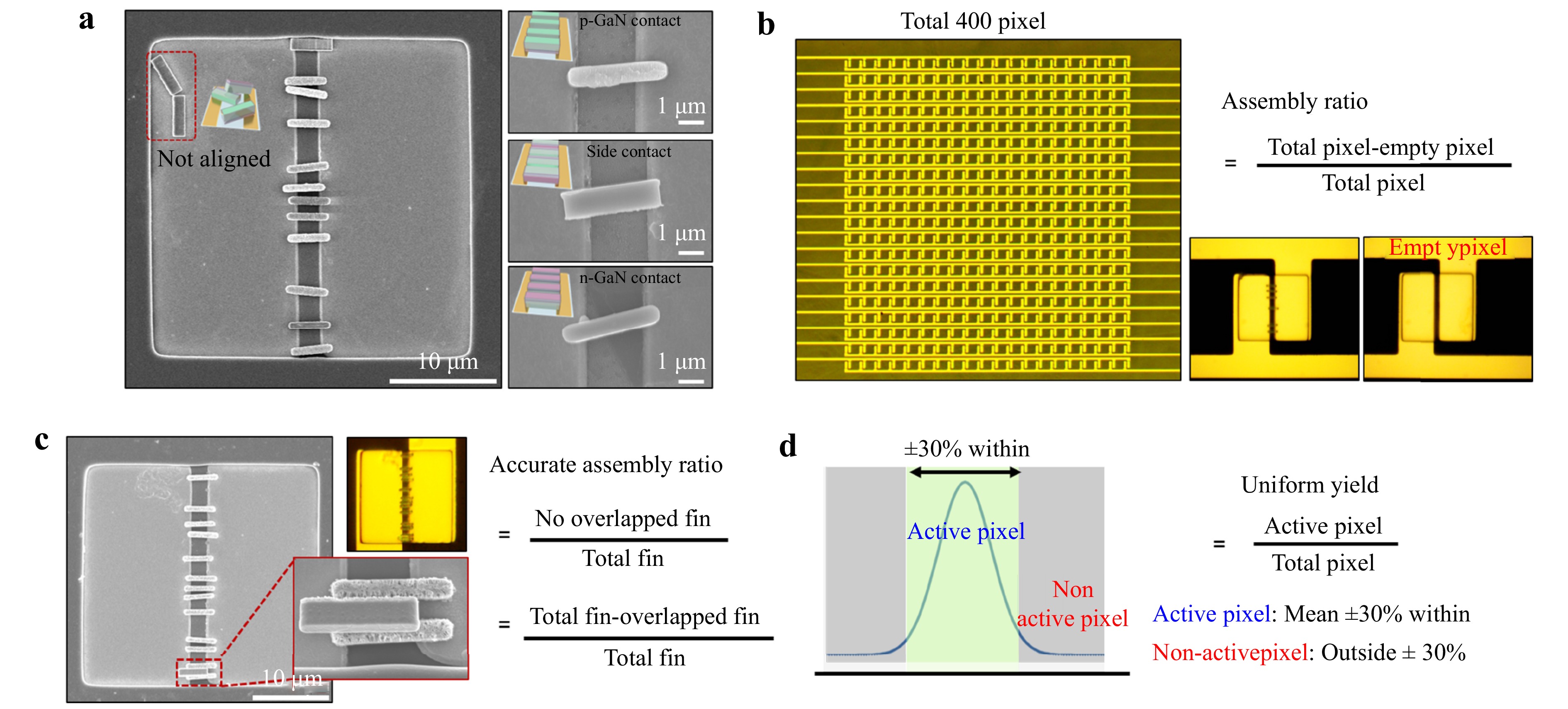
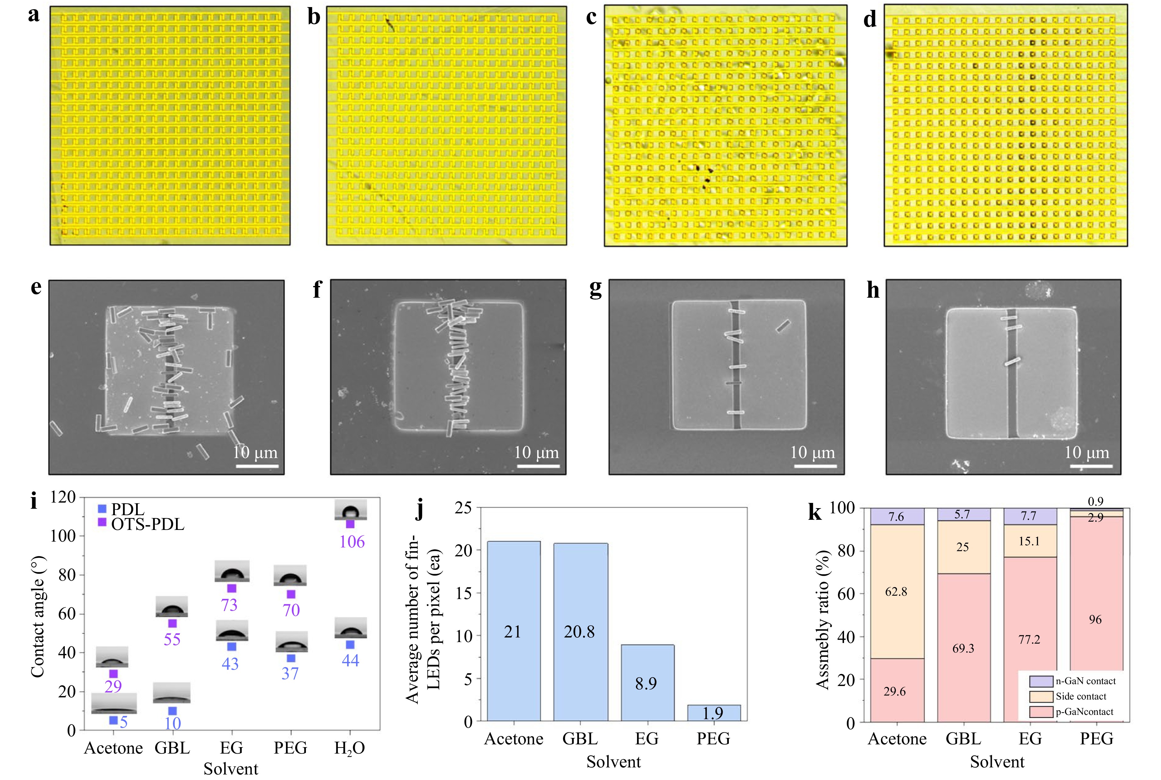
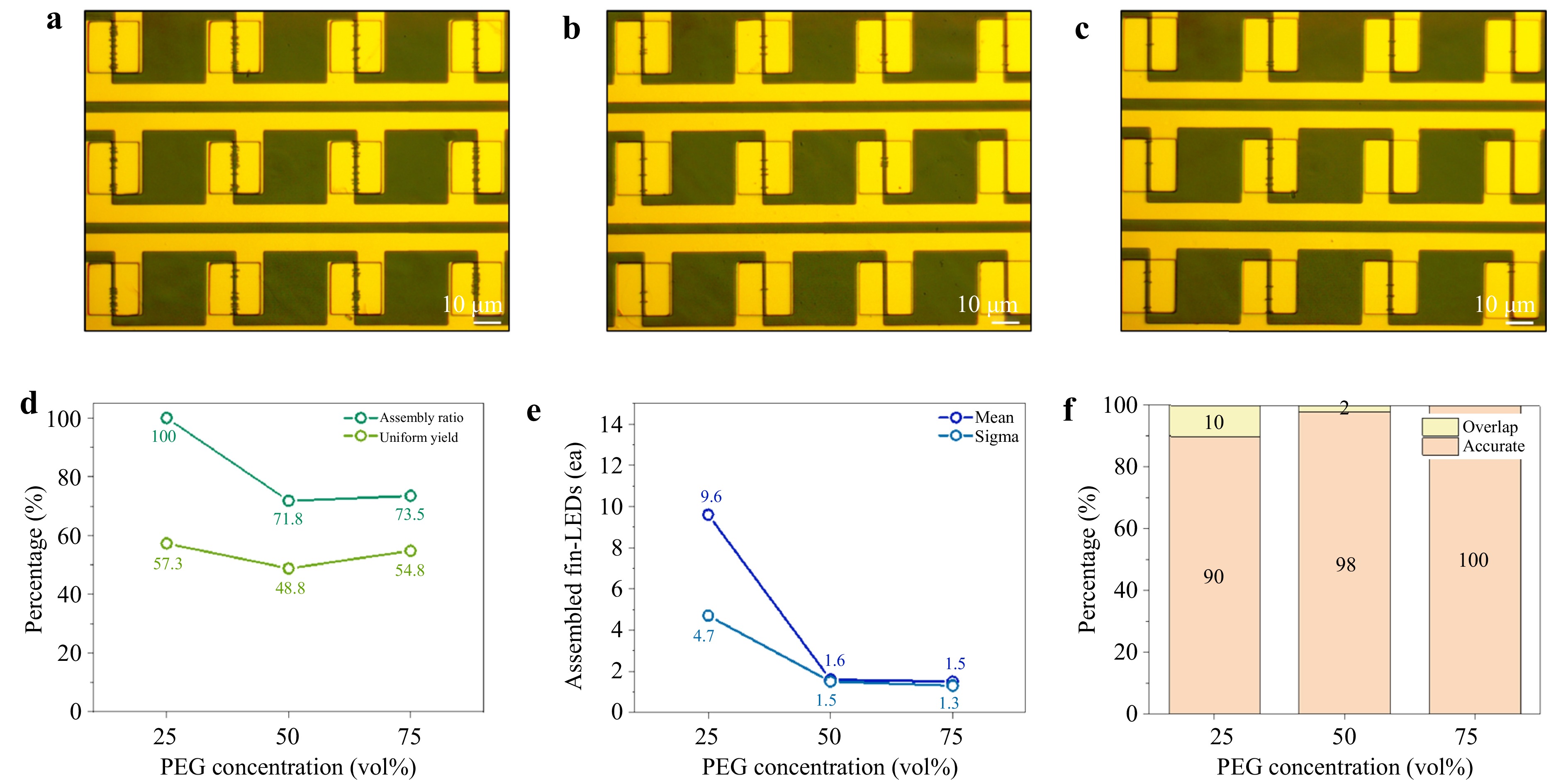
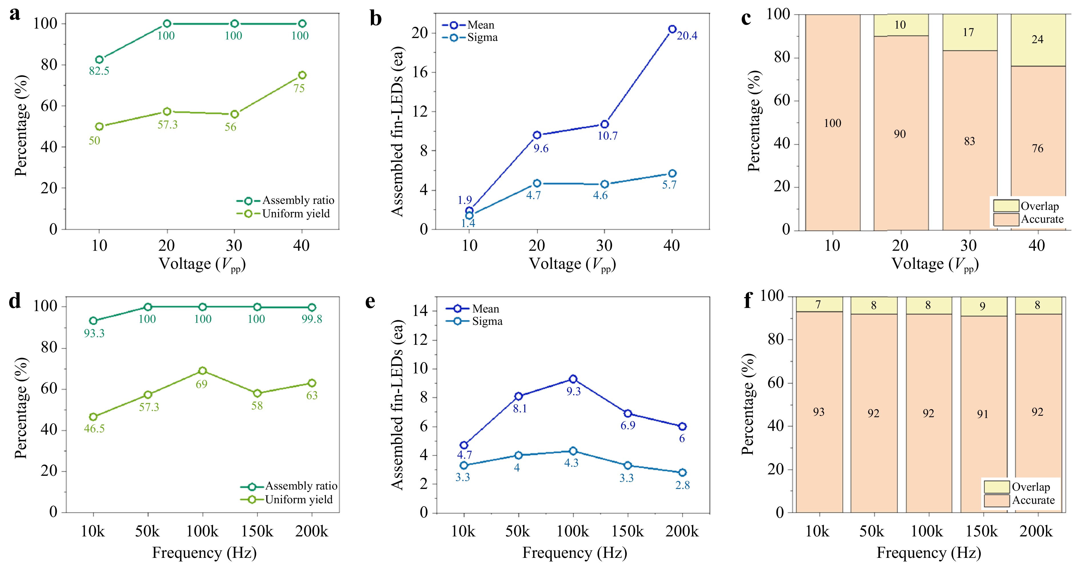
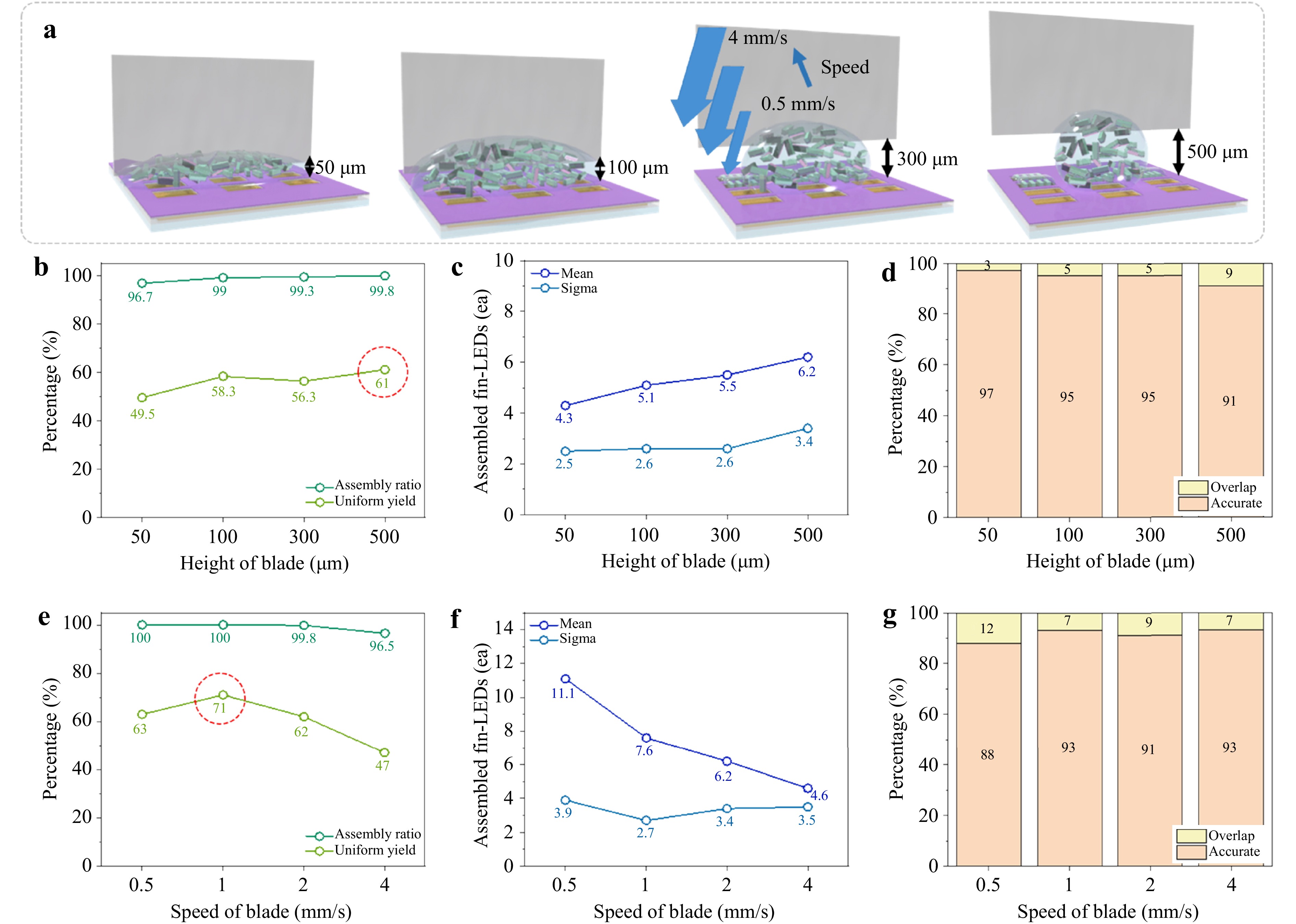
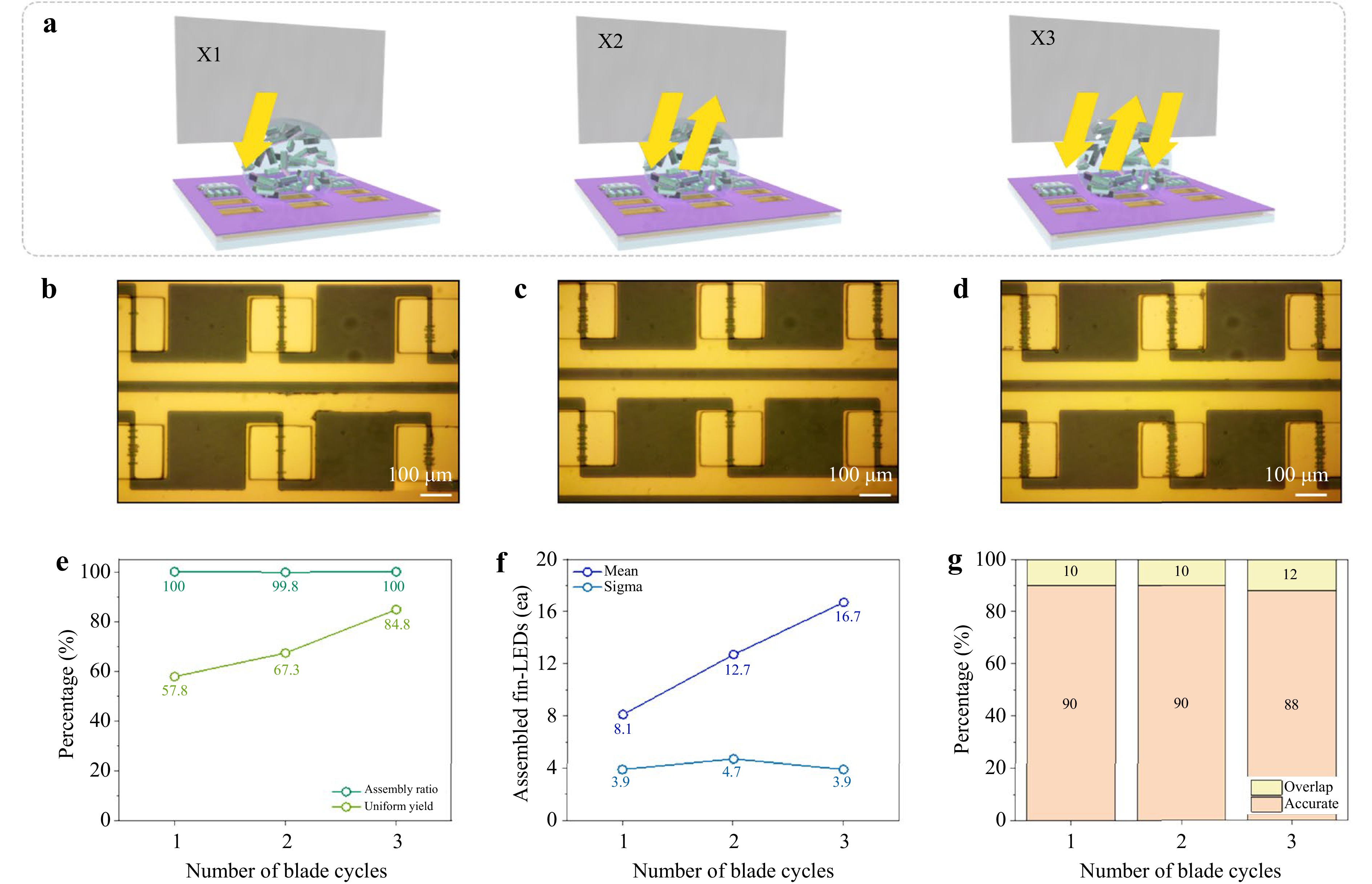
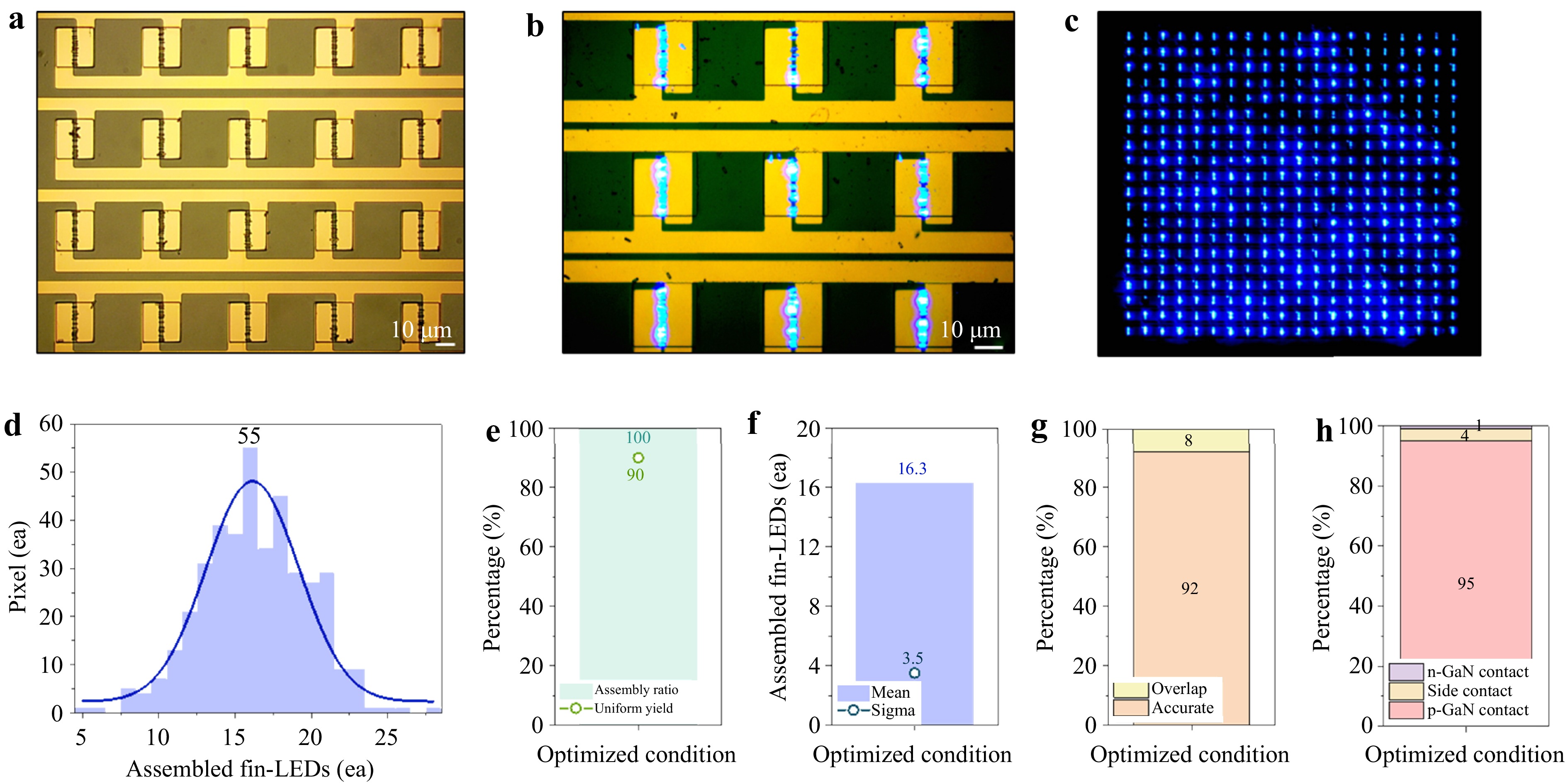
We propose a high-precision assembly technique for realizing high-resolution nano- to microscale displays using a trapped-assembly approach that integrates a doctor-blade-based ink-delivery system with dielectrophoresis (DEP)-induced assembly. Octadecyltrichlorosilane (OTS) self-assembled monolayers (SAMs) were coated onto the pixel-defined layer (PDL) to promote ink trapping and confine fin-LEDs within individual pixels during assembly. Key process parameters—including the viscosity and dielectric properties of the ink solvent, speed and number of blade passes, blade-to-substrate gap, and applied DEP voltage and frequency—were systematically optimised, as these parameters affect solvent confinement of the solvent and fin-LED assembly behavior. Under optimised conditions, achieved through precise control of solvent polarity, DEP force and torque, and doctor-blading parameters, all 400 pixels were successfully assembled. Statistical analysis revealed that 90% of the pixels contained 12-20 fin-LEDs, with an average of 16.3 fin-LEDs per pixel and a standard deviation of 3.5. The overlap ratio was limited to 8%, and 92% of the fin-LEDs were accurately assembled, of which 95% established contact with the p-GaN surface. Electroluminescent devices fabricated using the assembled fin-LEDs exhibited bright and uniform emission across the entire pixel array, confirming their excellent assembly quality and high electrical reliability. The DEP-based trapped-assembly method provides a reliable and scalable strategy for the practical integration of nano- to microscale LEDs in next-generation high-resolution display technologies.
Published
, Published online: 24 July 2026
, doi: 10.37188/lam.2026.086
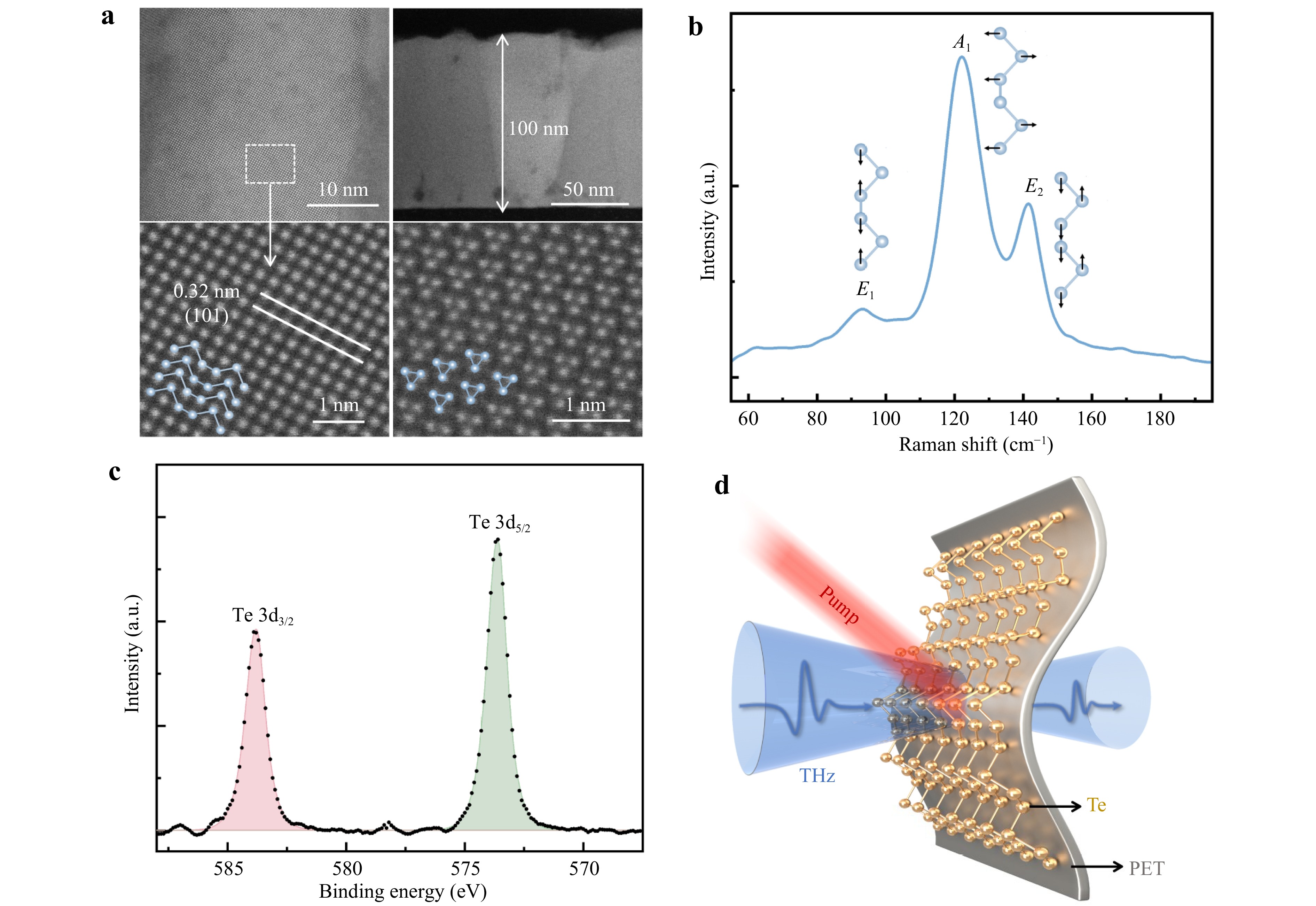
Flexible terahertz (THz) devices are fundamental components of wearable photonics and intelligent communication systems. However, conventional THz devices are affected by information loss or signal interruption due to mechanical deformation, which degrade their information fidelity. Here, we introduce tellurium (Te) nanofilms grown on polyethylene terephthalate (PET) substrates as a new class of mechanically robust THz modulators that can successfully improve device performances to optimal levels among existing flexible broadband modulators. The ultrafast transient THz photoresponses of two-dimensional Te films remained unchanged even after 1000 bending cycles or at a small bending radius of 3 mm, exhibiting high tolerance to bending deformation. Furthermore, the variations in the pattern recognition accuracy remained within 2% under different bending conditions, indicating its adaptability to various deformation conditions. This prototype lays the foundation for developing intelligent perception elements that operate stably under complex mechanical deformations.


Published
, Published online: 22 July 2026
, doi: 10.37188/lam.2026.075
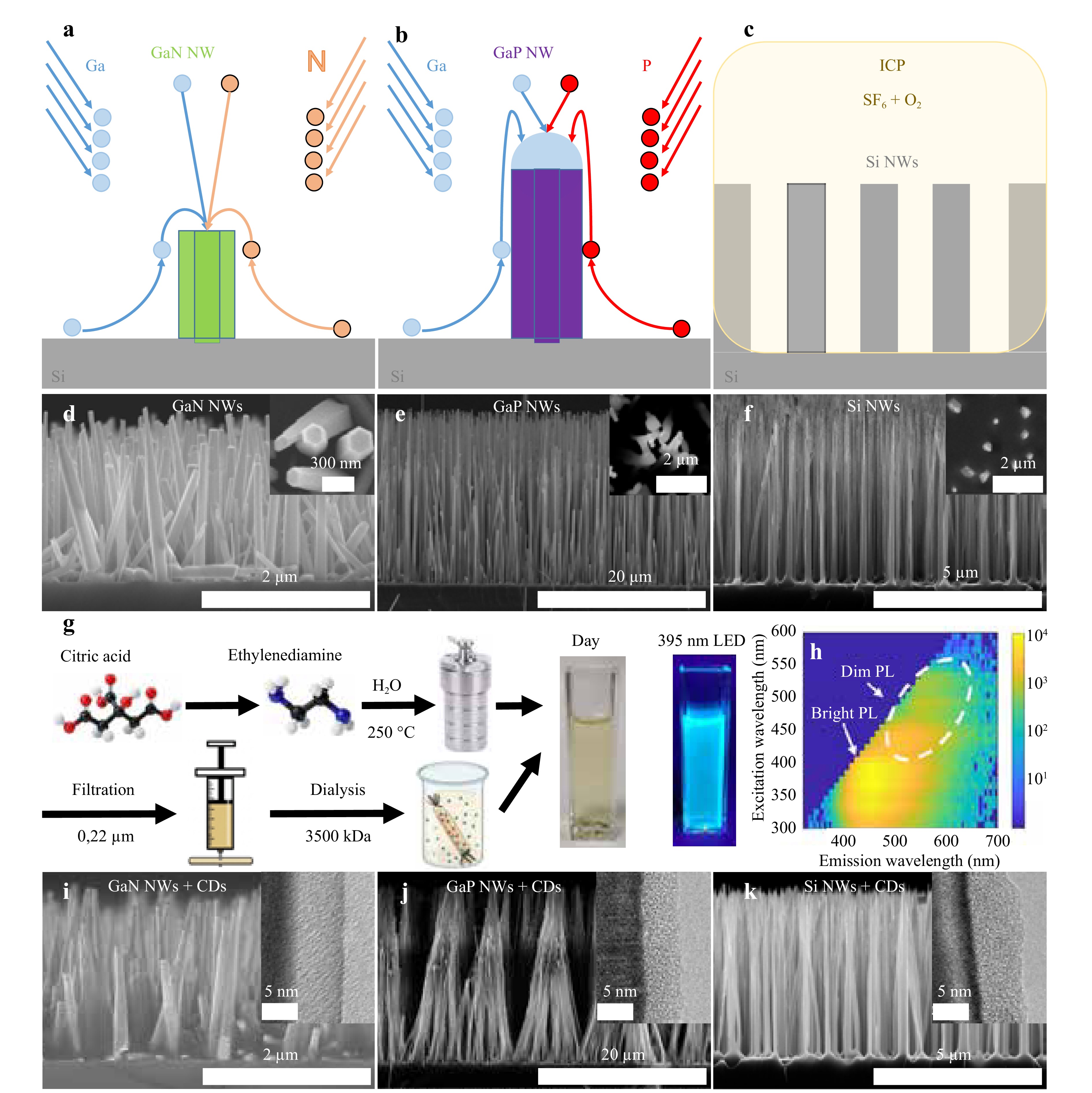
The integration of luminescent nanomaterials into scalable semiconductor platforms is vital for on-chip photonics. This study demonstrates an approach to fabricate fluorescent nanostructures by hybridising carbon dots (CDs) with semiconductor nanowires (NWs) grown on Si. We systematically investigated the photoluminescence of CDs on GaN, GaP, and Si NW hosts and demonstrated the key role of the absorption edge of the host as a practical spectral filter. Our results show that efficient CD excitation is governed by the transparency window of the NW, thereby allowing the precise tailoring of the emission spectrum through rational host selection. This effect has been consistently demonstrated in different materials. By coupling the tuneable chemistry of CDs with the tailored optoelectronics of semiconductor NWs, this study establishes a scalable host-guest architecture for engineering nanoscale light sources to promote applications in integrated photonic circuits and sensing.


Published
, Published online: 22 July 2026
, doi: 10.37188/lam.2026.098
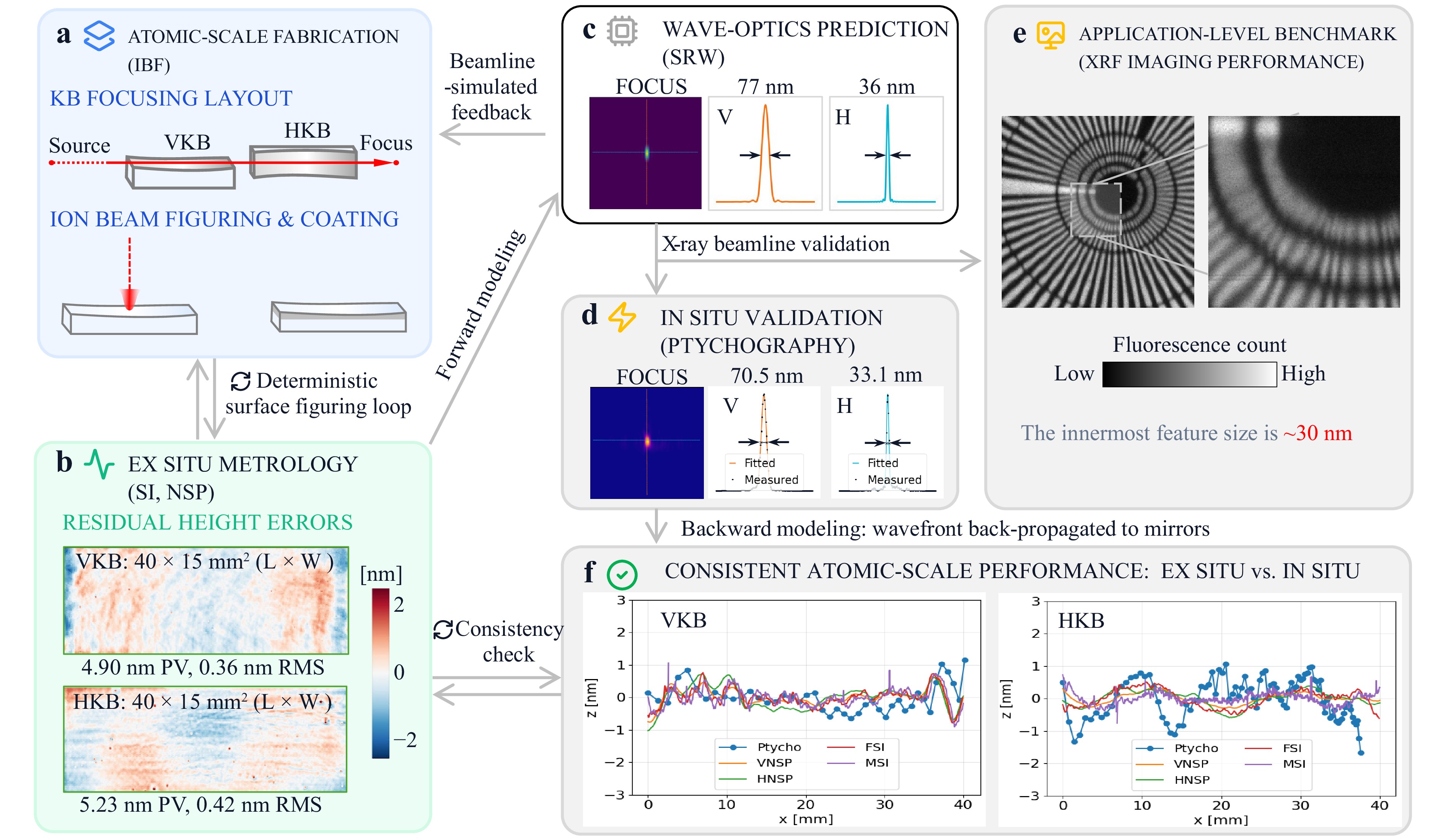
Diffraction-limited synchrotron sources place stringent demands on wavefront-preserving X-ray optics. We report a fully in-house, closed-loop pipeline at the National Synchrotron Light Source II that links ion beam figuring, precision ex situ metrology, wavefront simulation, and in situ beam validation. The fabricated elliptical Kirkpatrick–Baez mirrors achieved 0.4 nm root-mean-square residual height error. At 12 keV, ptychography measured a 70.5 × 33.1 nm2 (V × H) focal spot using an 8 × 7 µm2 secondary source aperture, consistent with partially coherent Synchrotron Radiation Workshop simulations of 77 × 36 nm2. X-ray fluorescence imaging independently resolved approximately 30 nm features in a Siemens star. Back-propagation of the reconstructed probe further linked the measured wavefront to ex situ surface errors, establishing quantitative closure across fabrication, metrology, simulation, and beamline commissioning.


Published
, Published online: 22 July 2026
, doi: 10.37188/lam.2026.083
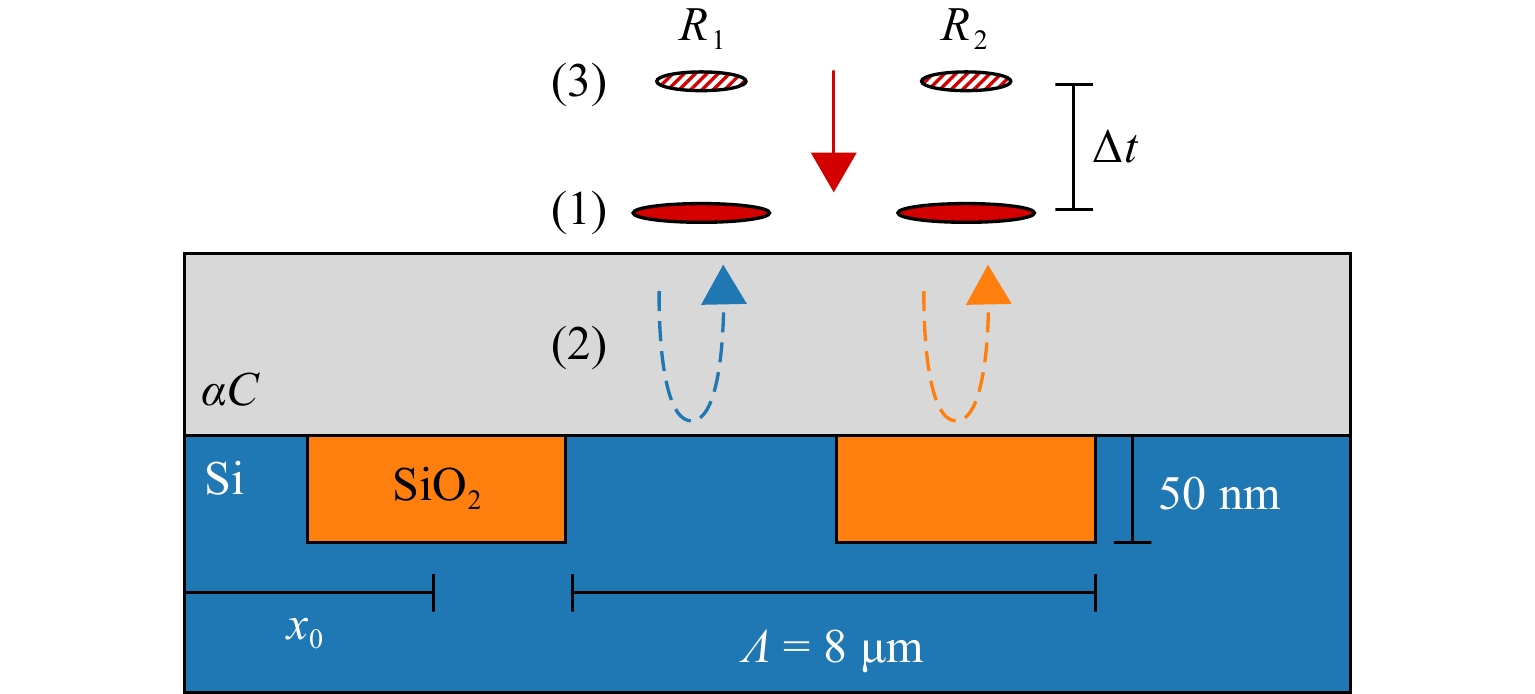
Manufacturing integrated circuits (ICs) using photolithography is the key technology enabling modern electronic devices. As advanced ICs are fabricated in multiple lithography steps, accurate metrology is crucial. For wafer alignment, optical methods are essential as they enable fast and non-invasive measurements. However, the use of optically opaque materials complicates optical metrology on markers in deeper layers. Here we present an optical metrology approach capable of nanometer-level alignment metrology through optically opaque layers. We use ultrashort laser pulses to generate high-frequency ultrasound at picosecond timescales, with which buried metrology markers can be probed. By detecting the ultrasound reflections with a second, time-delayed laser pulse, position information is obtained in an all-optical way. We demonstrate our approach on an alignment grating covered by a 1.3 μm thick layer of amorphous carbon, achieving 15 nm positioning reproducibility in 1 s measurement time, with significant potential for further scaling. This measurement concept will help advance semiconductor manufacturing, by enabling optical wafer metrology on future devices featuring layers of metals and other opaque materials.


Published
, Published online: 28 March 2026
, doi: 10.37188/lam.2026.032
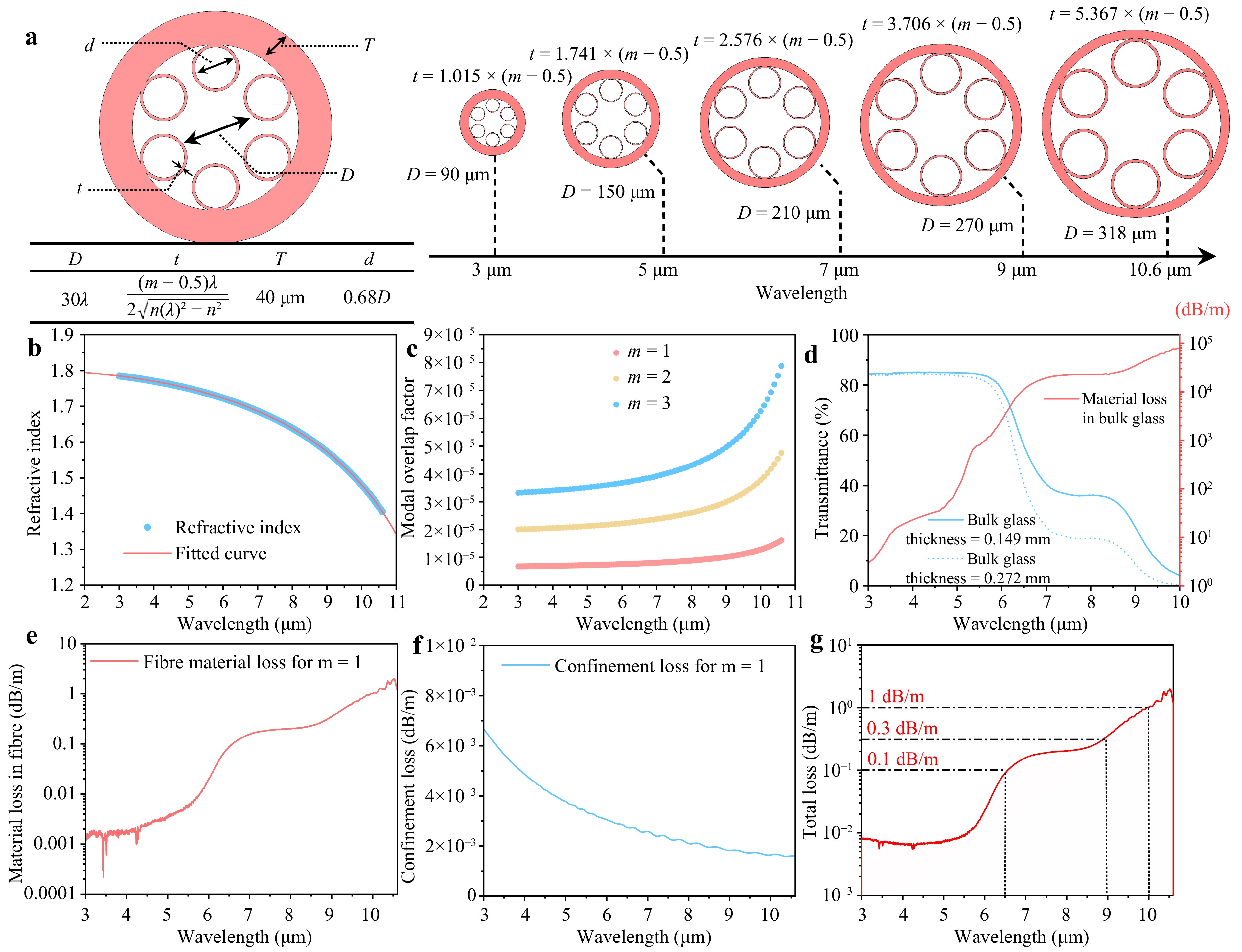
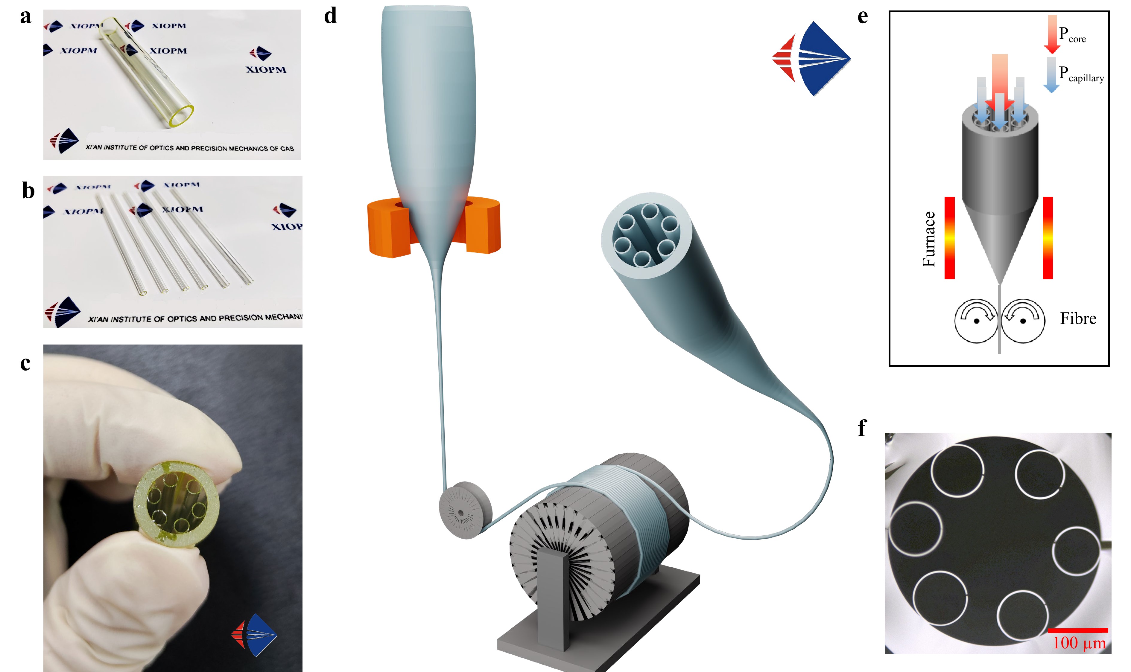
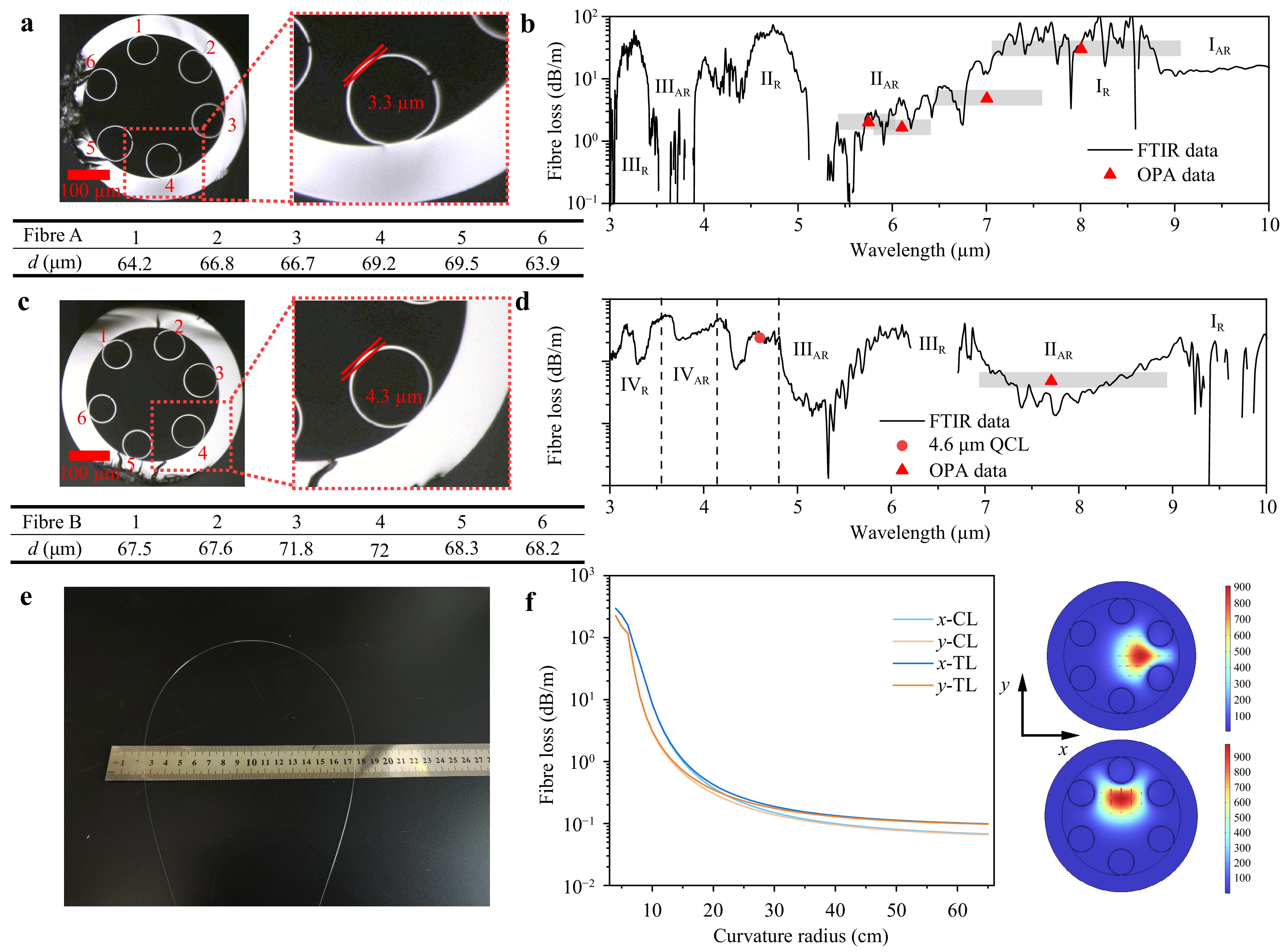
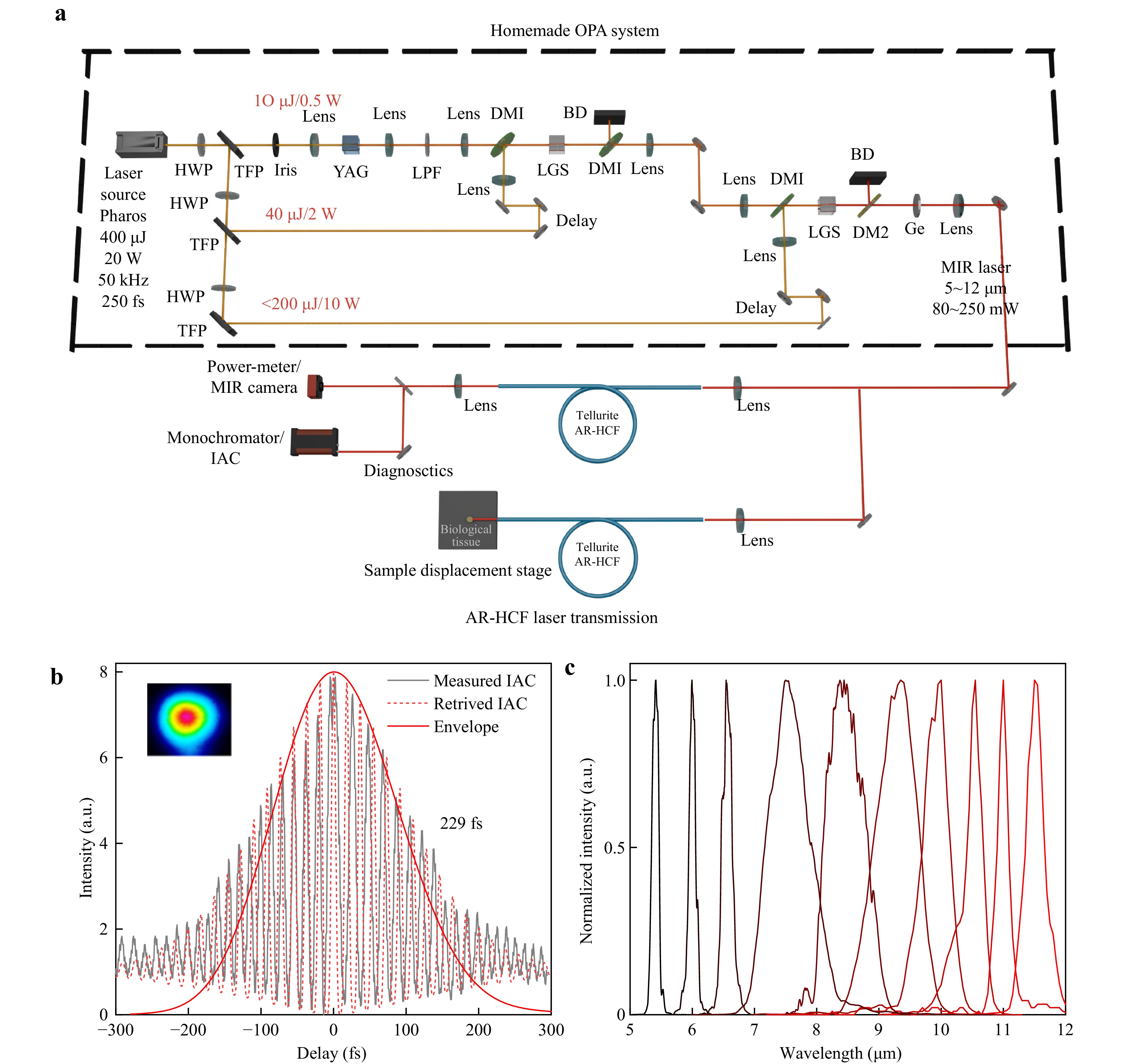
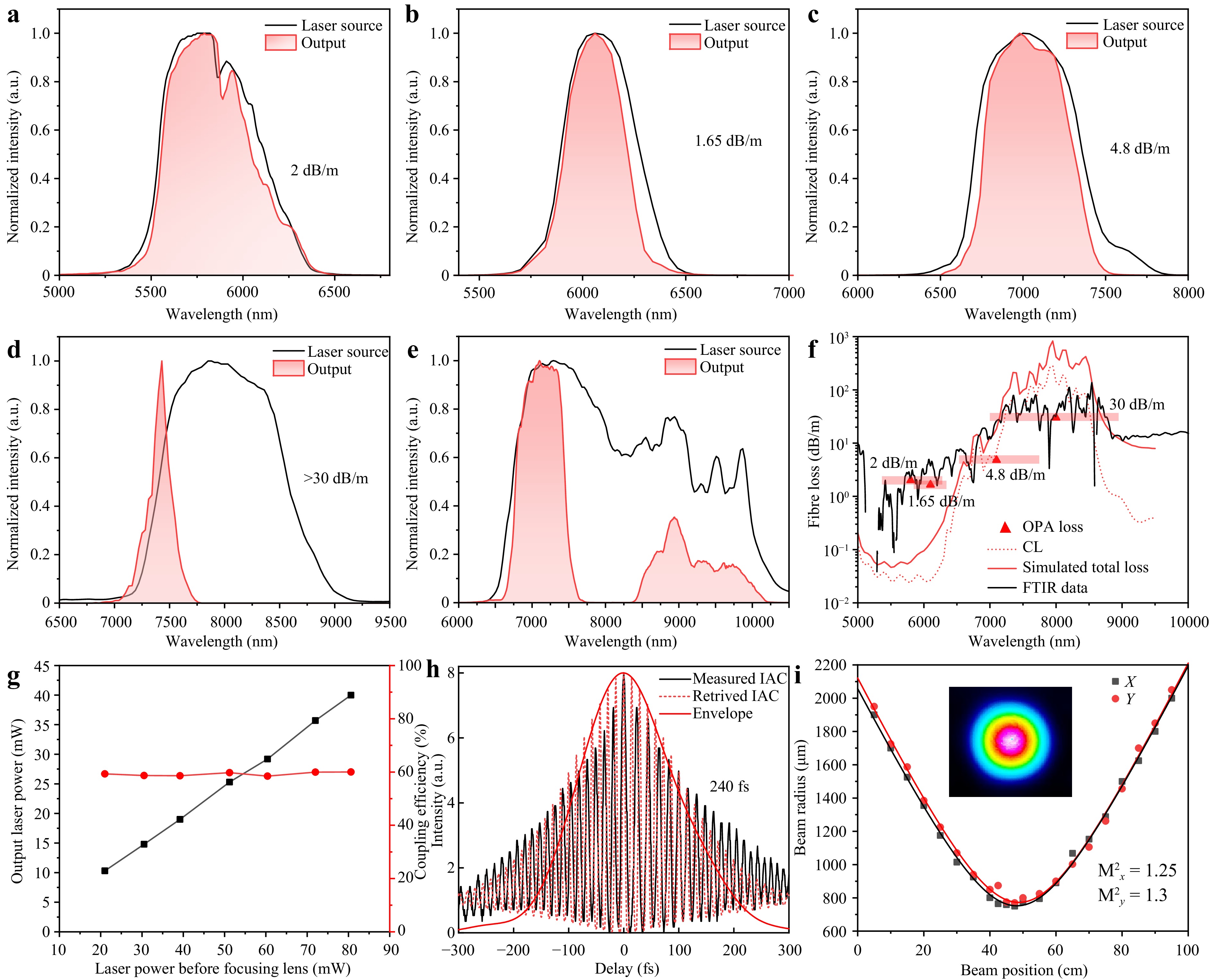
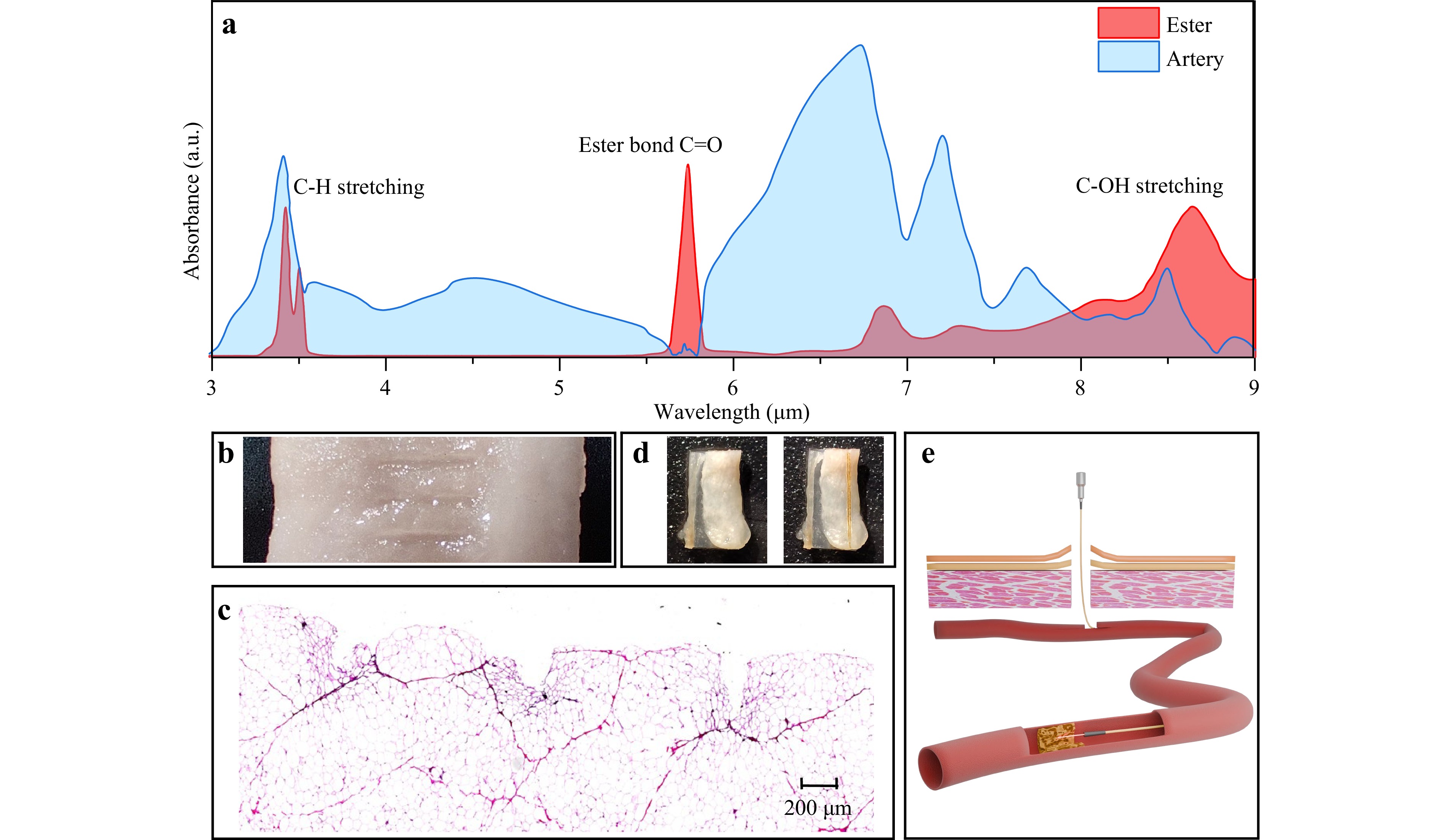
The absence of flexible fibres capable of delivering high-intensity mid-infrared ultrafast lasers (particularly at wavelengths exceeding 5 μm) without inducing pulse distortion or material damage constitutes a major limitation for numerous applications, including laser-based minimally invasive surgery, precision materials processing, and gas sensing. Herein, a tellurite glass anti-resonant hollow-core fibre is proposed that exhibits low transmission loss across the 5–10 μm band (~2 dB/m at 5.5–6 μm or 7.5–8 μm), robust bending resilience (minimum radius of 8 cm), and improved beam quality (output M2 reduced from 1.5 to 1.25). Notably, it facilitates the distortion-free delivery of ultrafast mid-infrared pulses from an optical parametric amplification system, without causing spectral broadening or material damage, at an input peak power of 16 MW. In a proof-of-concept demonstration, the developed fibre enables wavelength-selective ablation of biological adipose tissue at 5.75 μm, representing, to the best of our knowledge, the first such demonstration using tellurite hollow-core fibre platform. A record-wide operational bandwidth, extending to 10 μm, is achieved by leveraging the extended infrared edge of tellurite glass. This study confirms that tellurite anti-resonant hollow-core fibres can serve as groundbreaking tools in ultrafast mid-infrared photonics, offering significant potential for addressing challenges in invasive laser surgery, gas-phase spectroscopy, and non-linear optical studies.
Published
, Published online: 01 December 2023
, doi: 10.37188/lam.2023.036
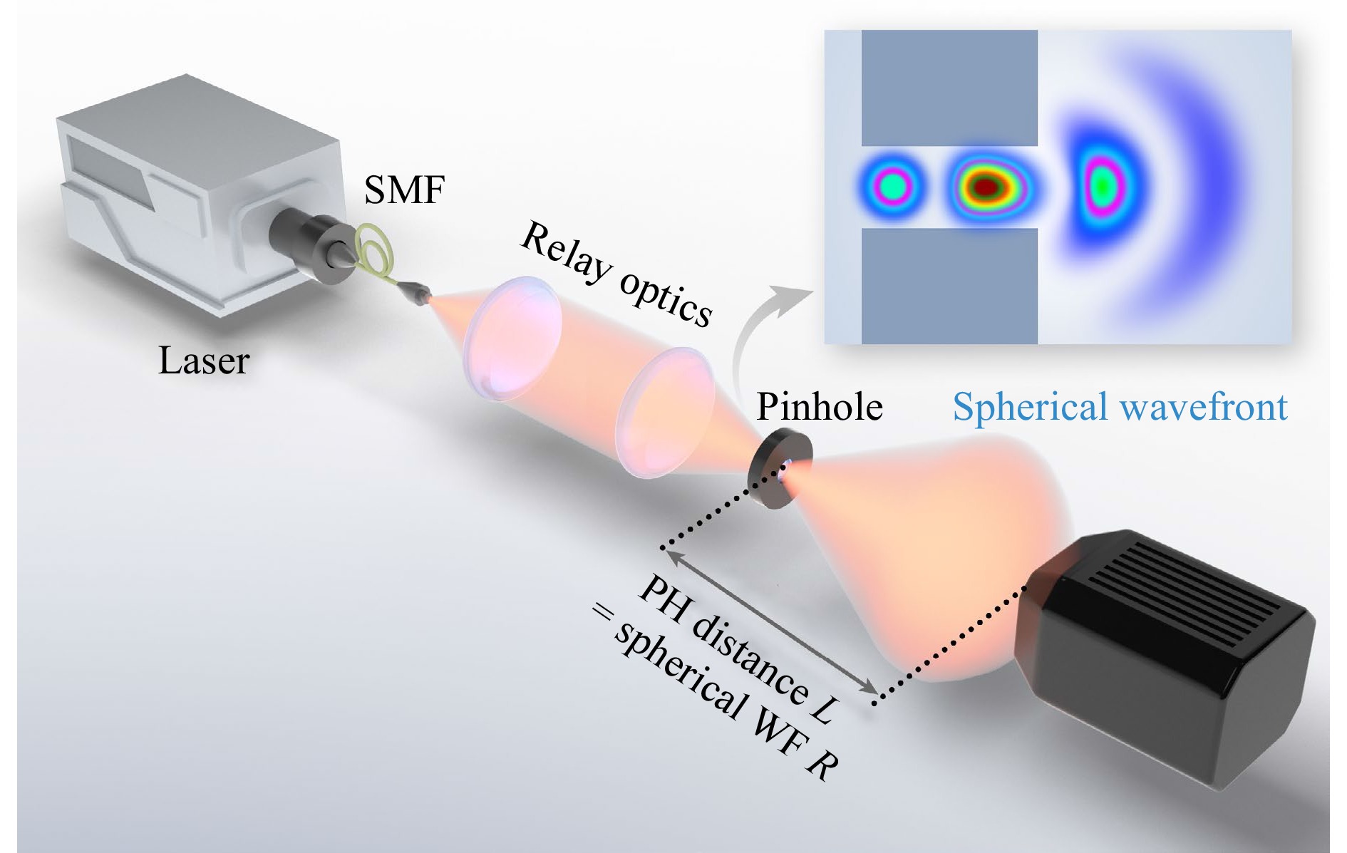
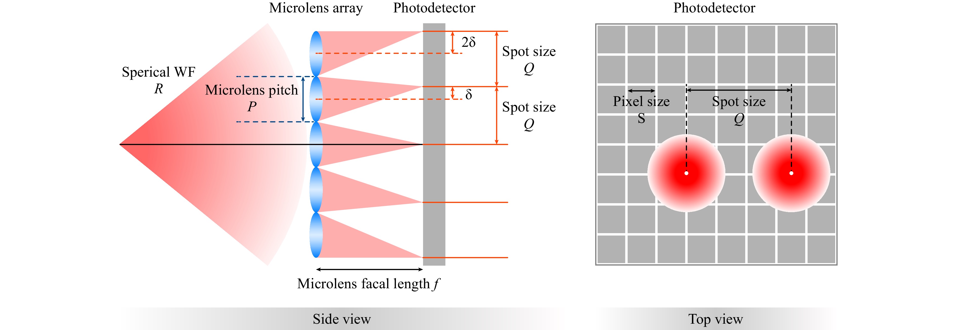
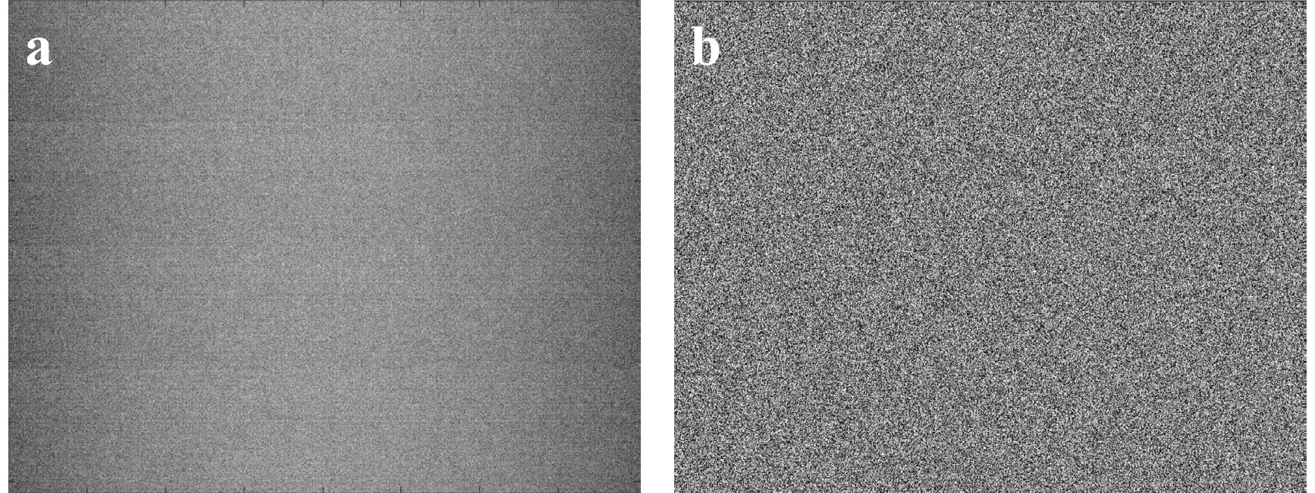
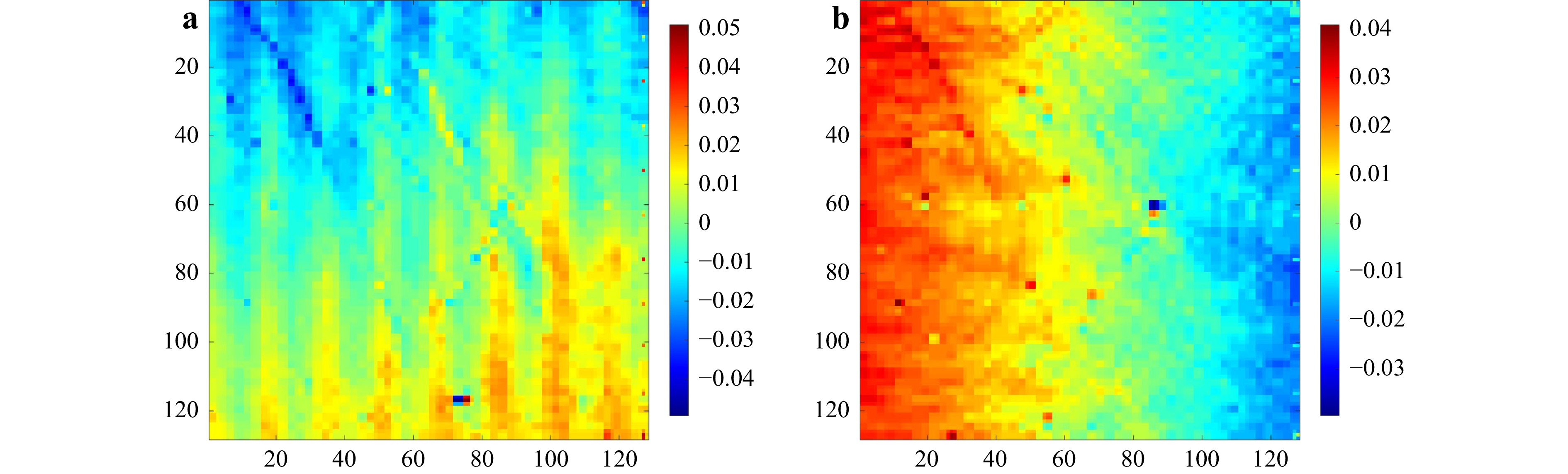
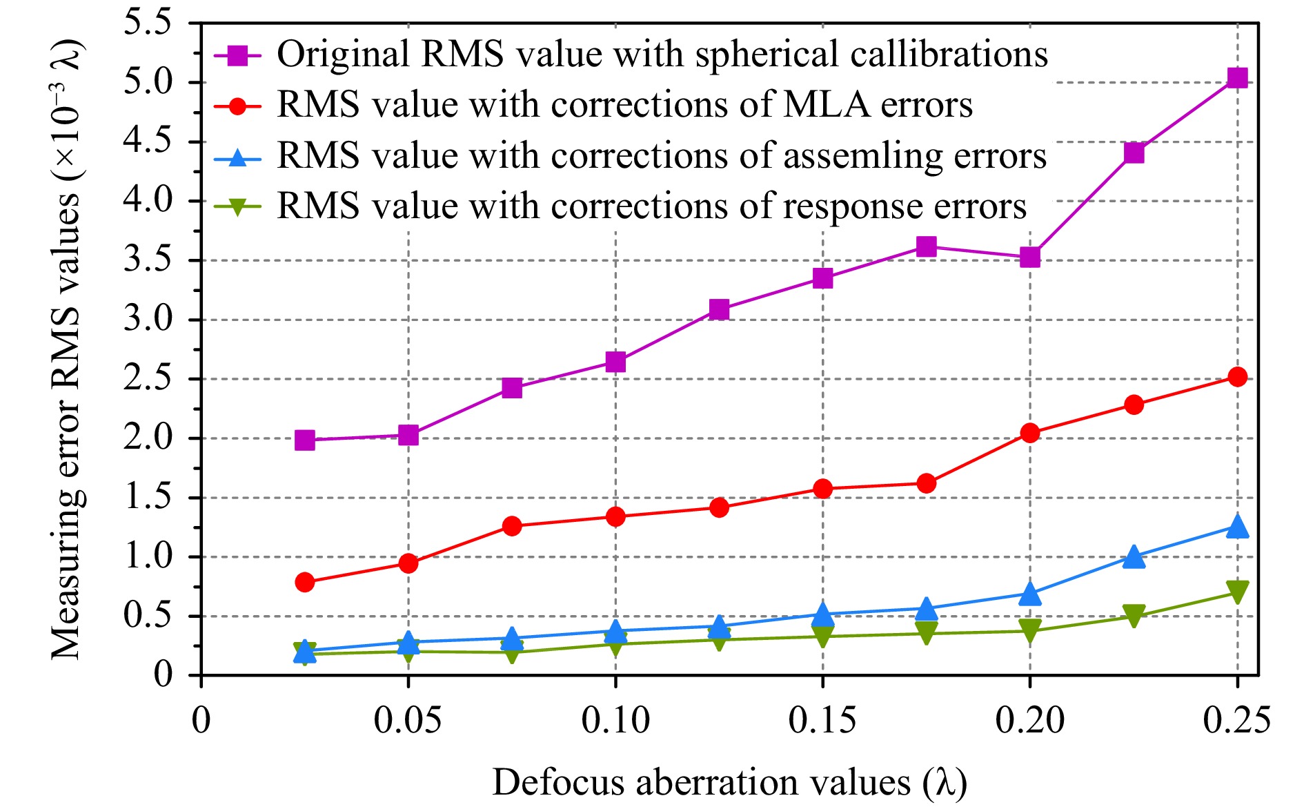
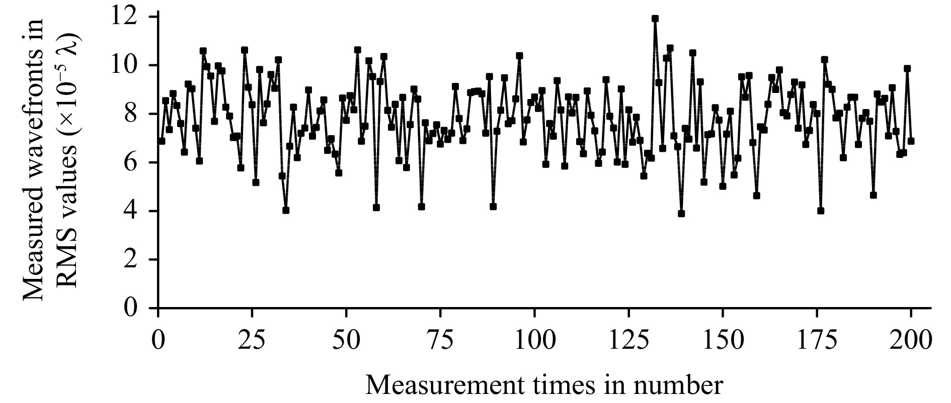
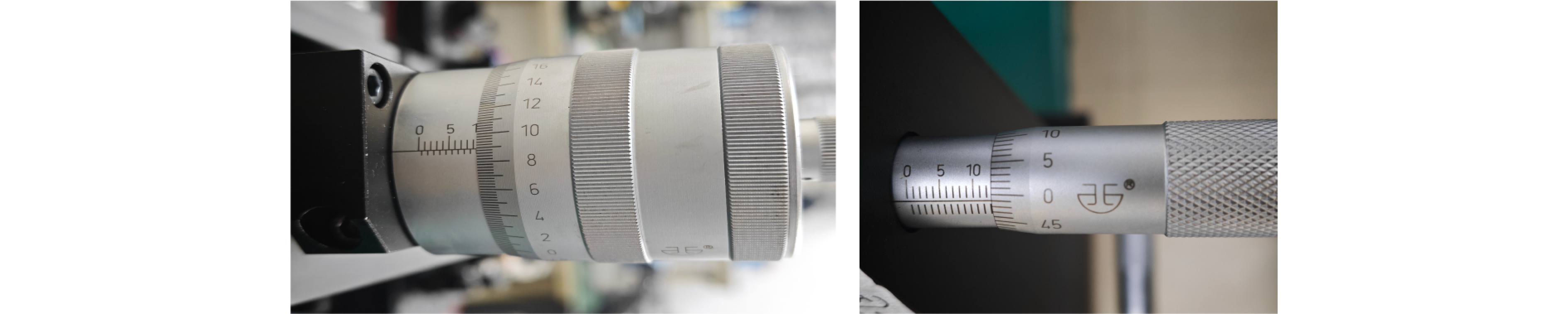
The widely used Shack–Hartmann wavefront sensor (SHWFS) is a wavefront measurement system. Its measurement accuracy is limited by the reference wavefront used for calibration and also by various residual errors of the sensor itself. In this study, based on the principle of spherical wavefront calibration, a pinhole with a diameter of 1 µm was used to generate spherical wavefronts with extremely small wavefront errors, with residual aberrations of 1.0 × 10⁻⁴ λ RMS, providing a high-accuracy reference wavefront. In the first step of SHWFS calibration, we demonstrated a modified method to solve for three important parameters (f, the focal length of the microlens array (MLA), p, the sub-aperture size of the MLA, and s, the pixel size of the photodetector) to scale the measured SHWFS results. With only three iterations in the calculation, these parameters can be determined as exact values, with convergence to an acceptable accuracy. For a simple SHWFS with an MLA of 128 × 128 sub-apertures in a square configuration and a focal length of 2.8 mm, a measurement accuracy of 5.0 × 10⁻³ λ RMS was achieved across the full pupil diameter of 13.8 mm with the proposed spherical wavefront calibration. The accuracy was dependent on the residual errors induced in manufacturing and assembly of the SHWFS. After removing these residual errors in the measured wavefront results, the accuracy of the SHWFS increased to 1.0 × 10⁻³ λ RMS, with measured wavefronts in the range of λ/4. Mid-term stability of wavefront measurements was confirmed, with residual deviations of 8.04 × 10⁻⁵ λ PV and 7.94 × 10⁻⁵ λ RMS. This study demonstrates that the modified calibration method for a high-accuracy spherical wavefront generated from a micrometer-scale pinhole can effectively improve the accuracy of an SHWFS. Further accuracy improvement was verified with correction of residual errors, making the method suitable for challenging wavefront measurements such as in lithography lenses, astronomical telescope systems, and adaptive optics.
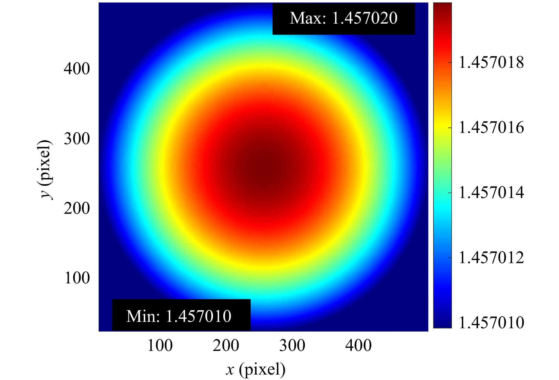
Published
, Published online: 29 April 2026
, doi: 10.37188/lam.2026.053
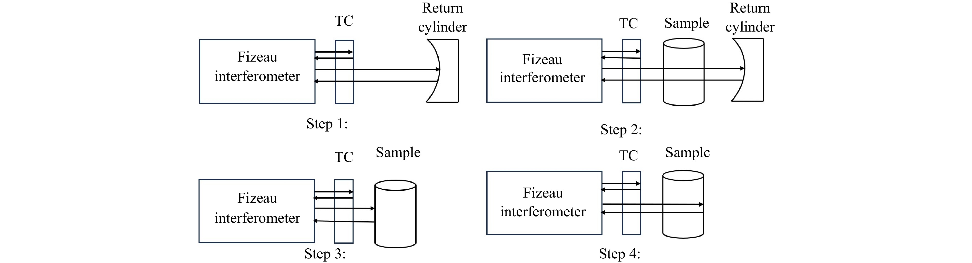
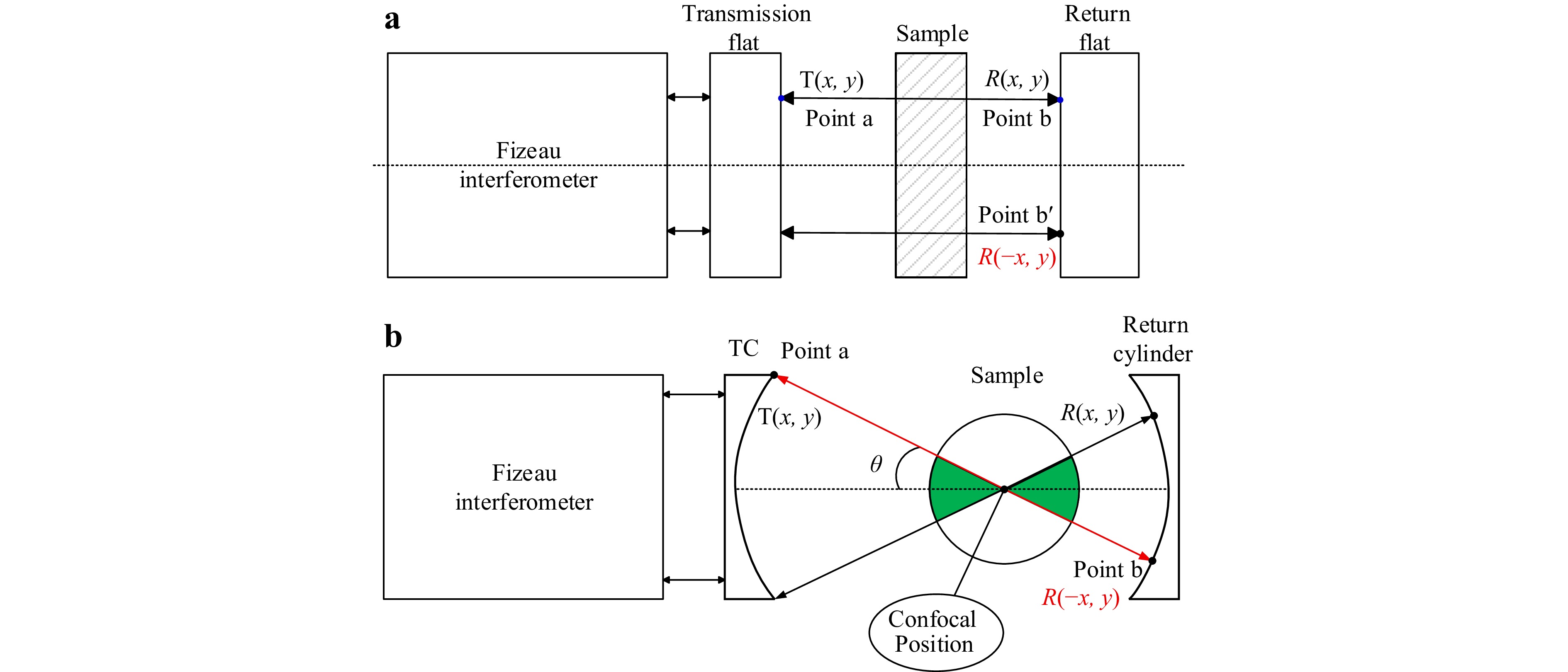
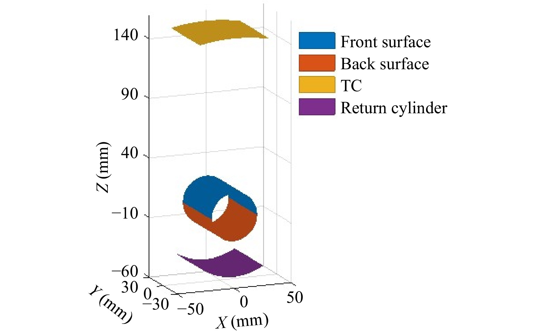
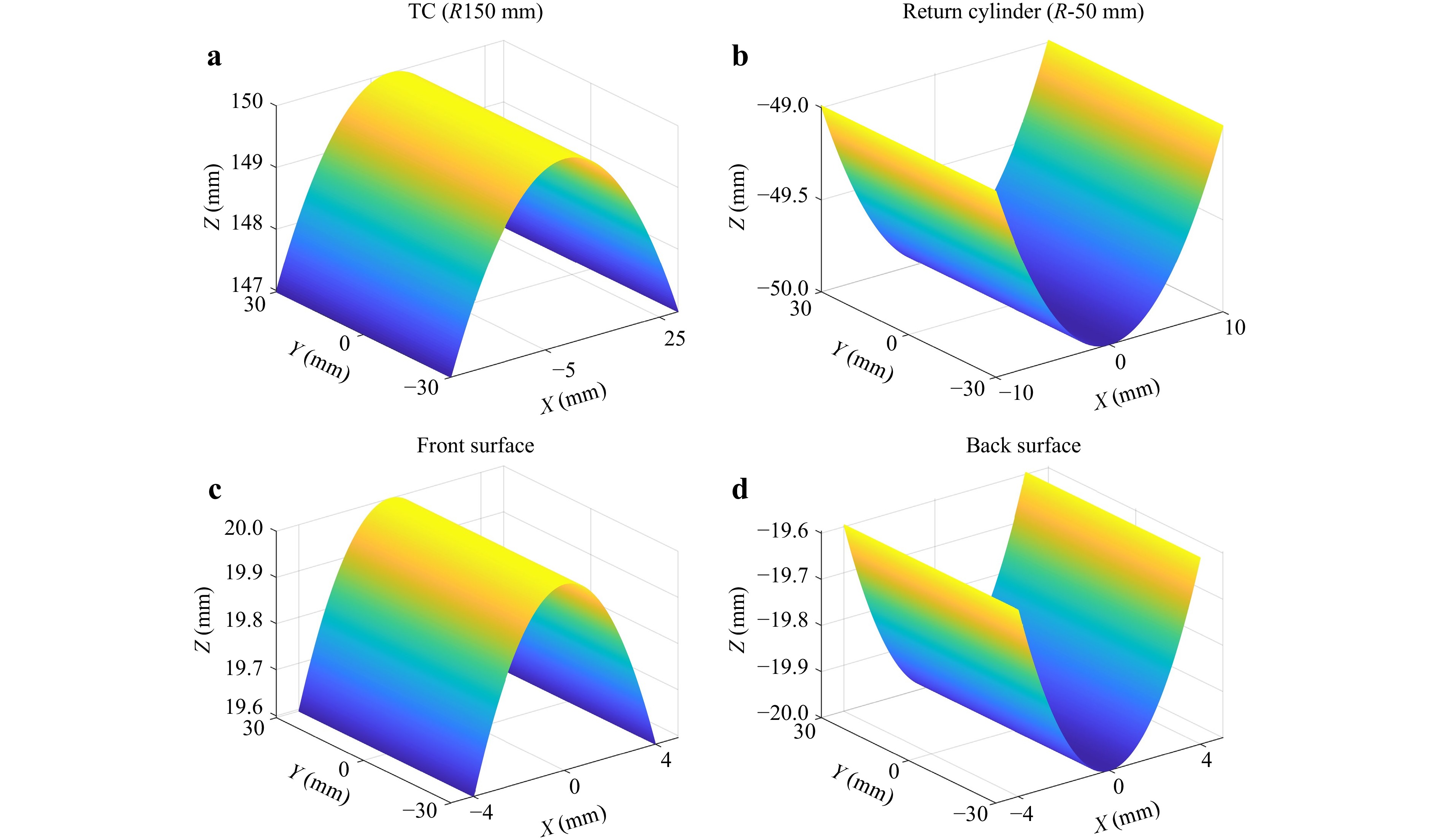
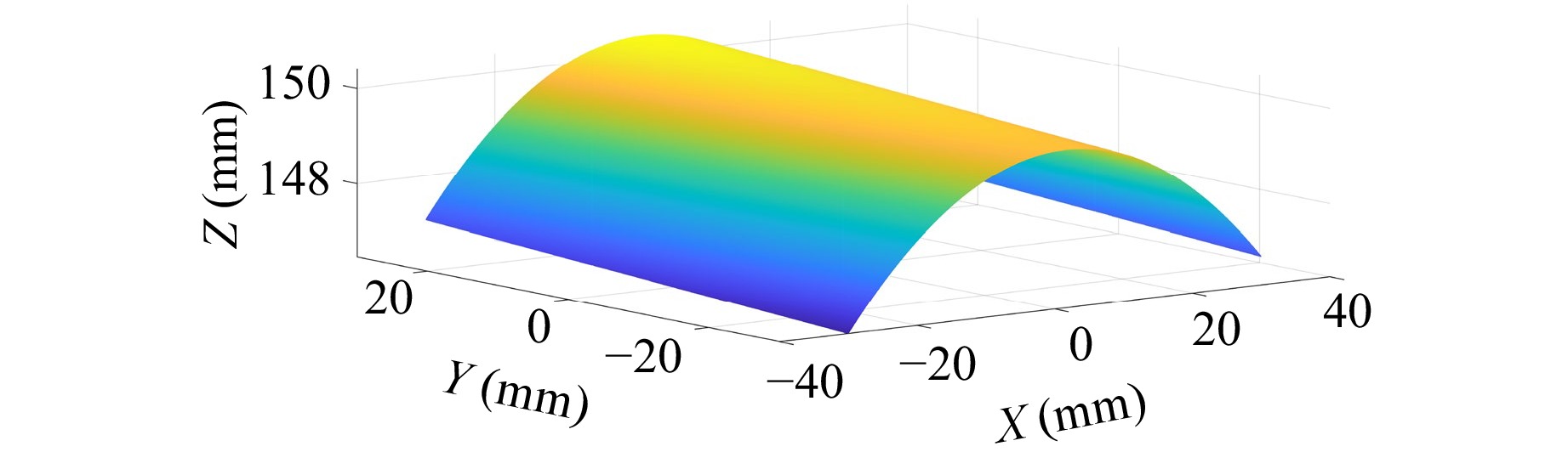
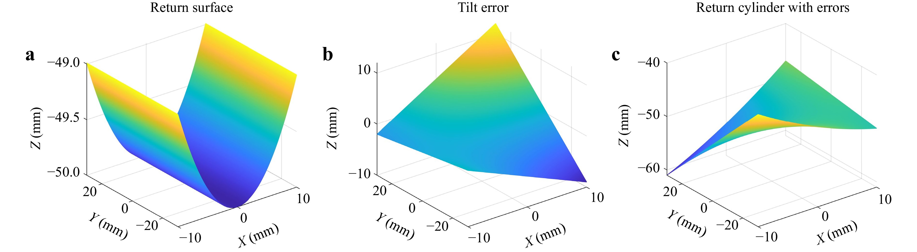
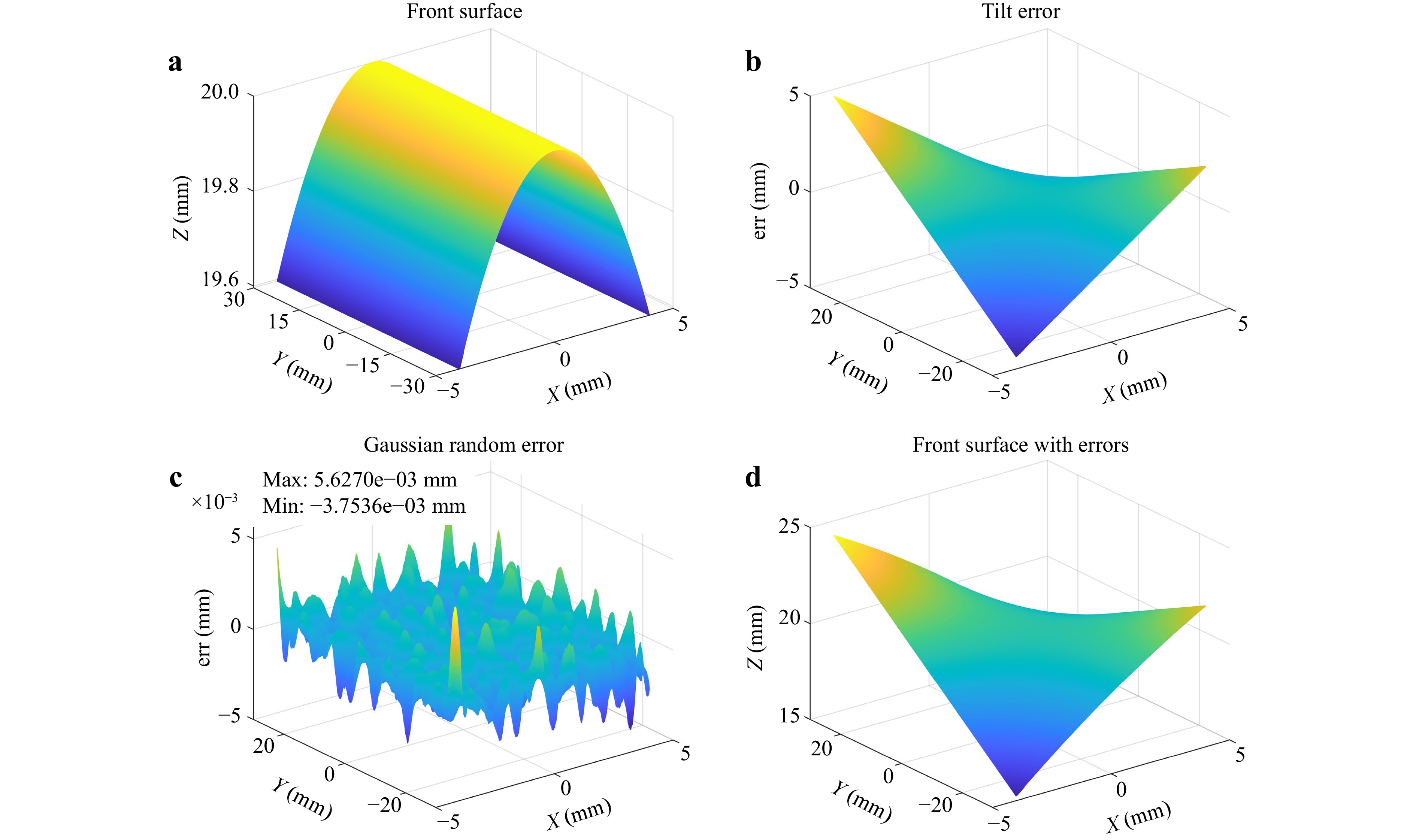
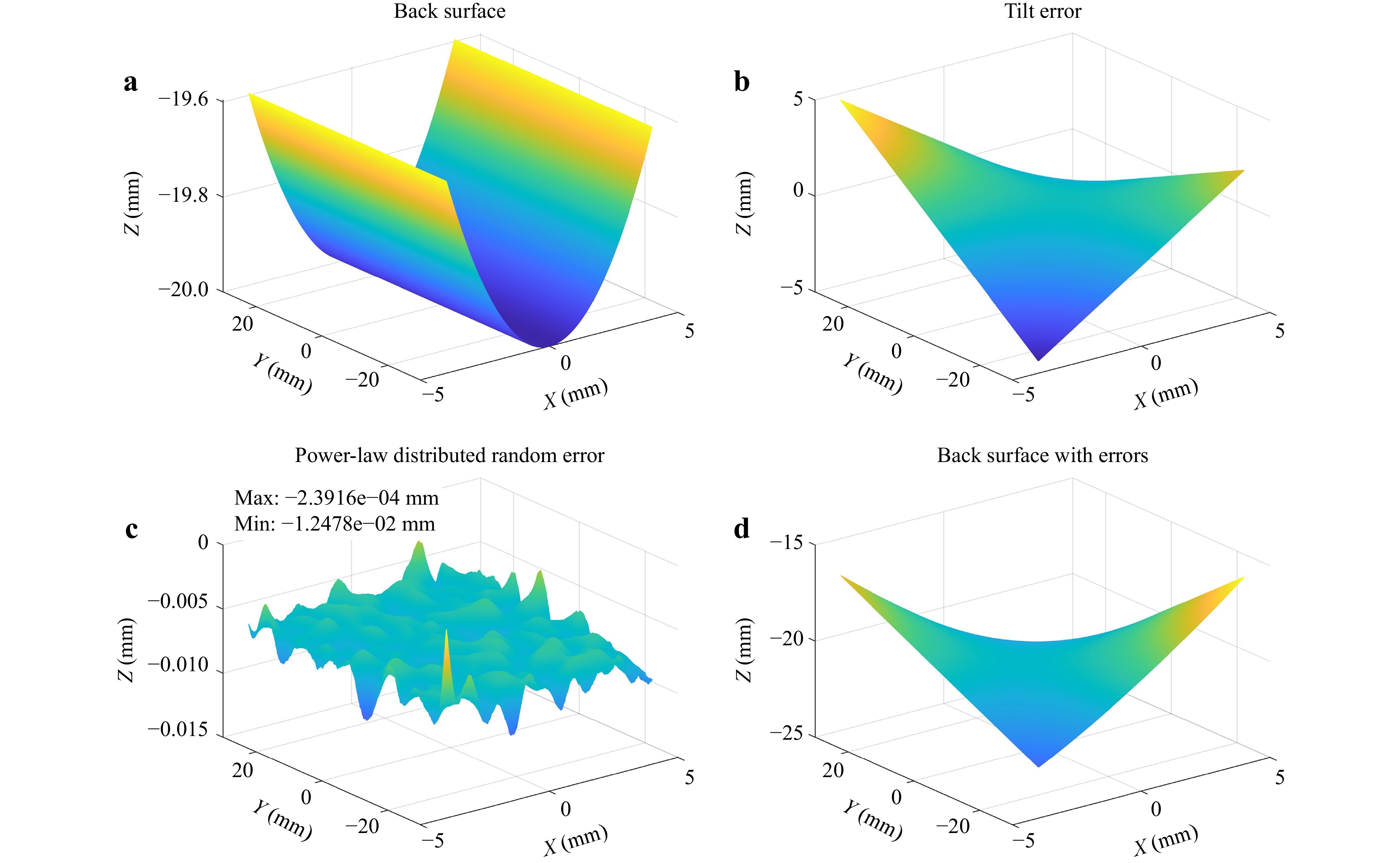
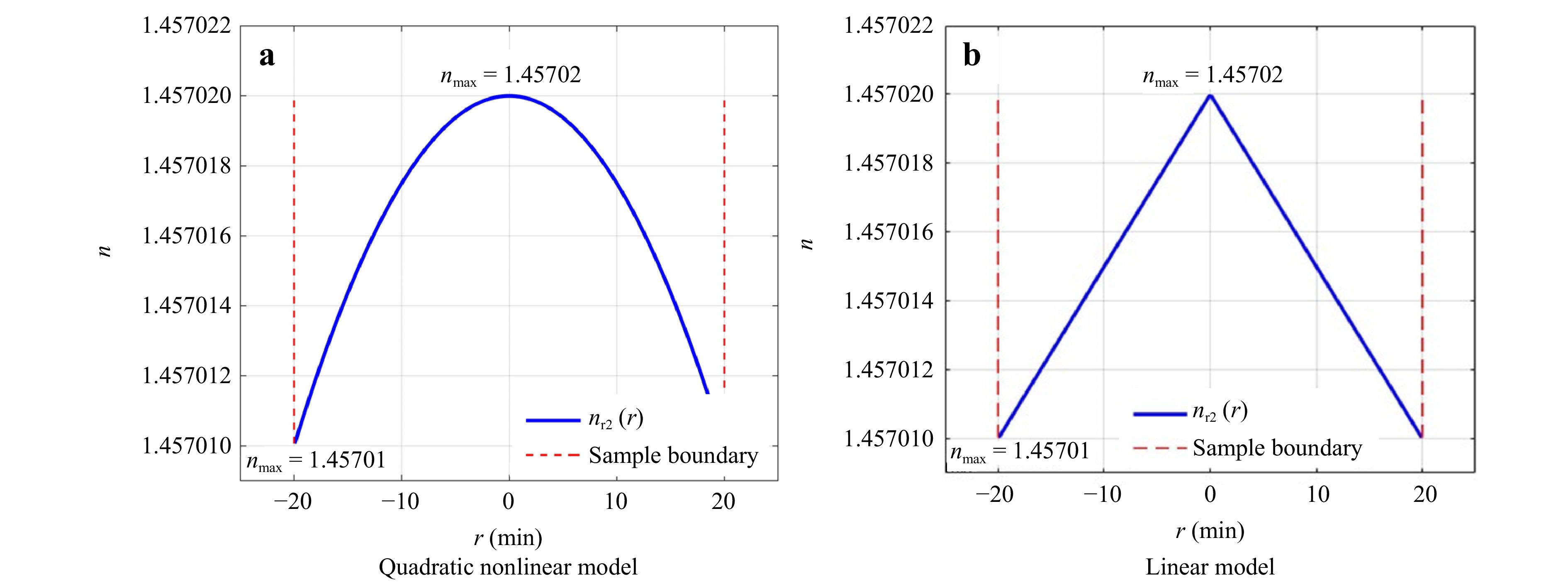
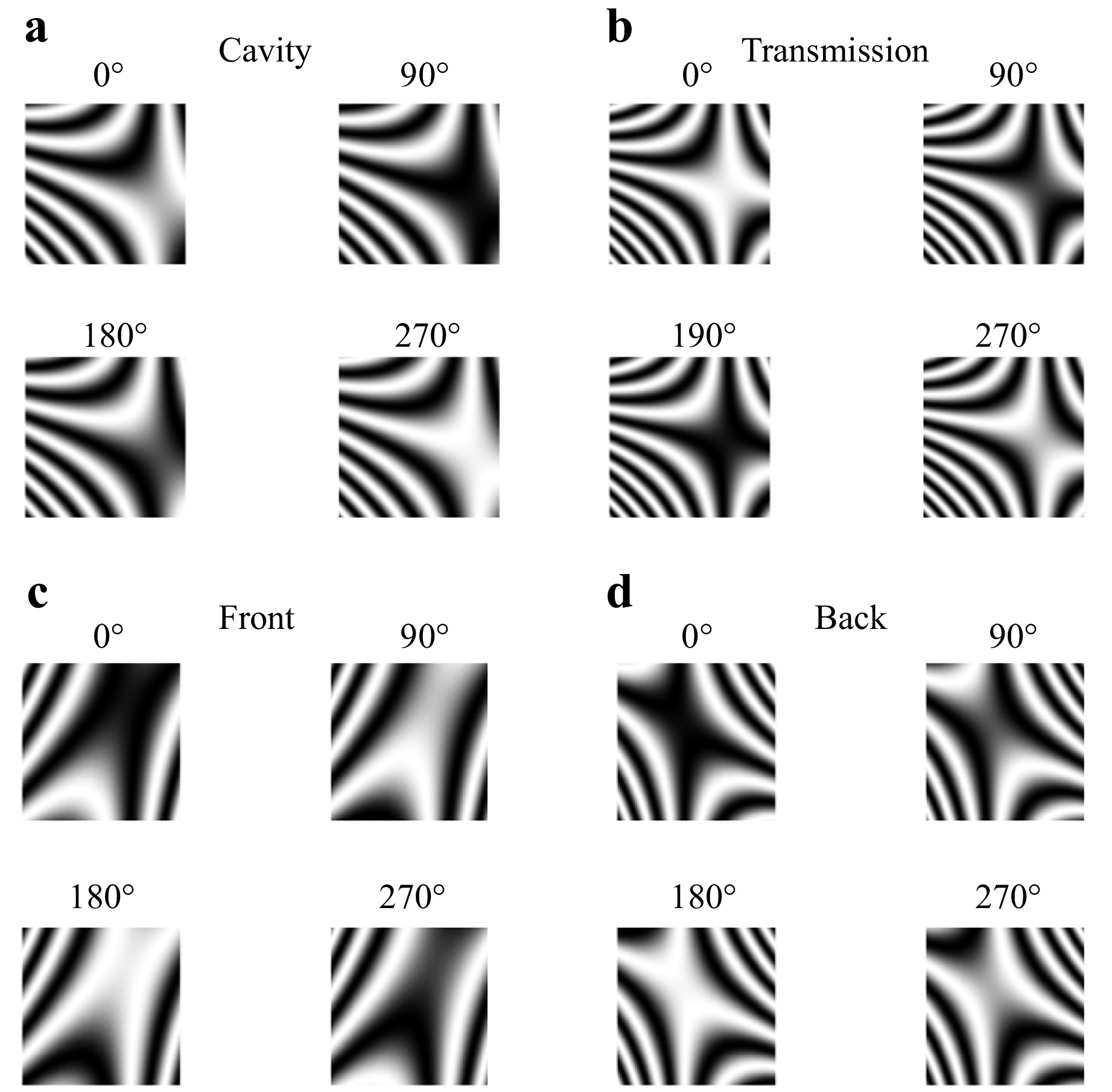
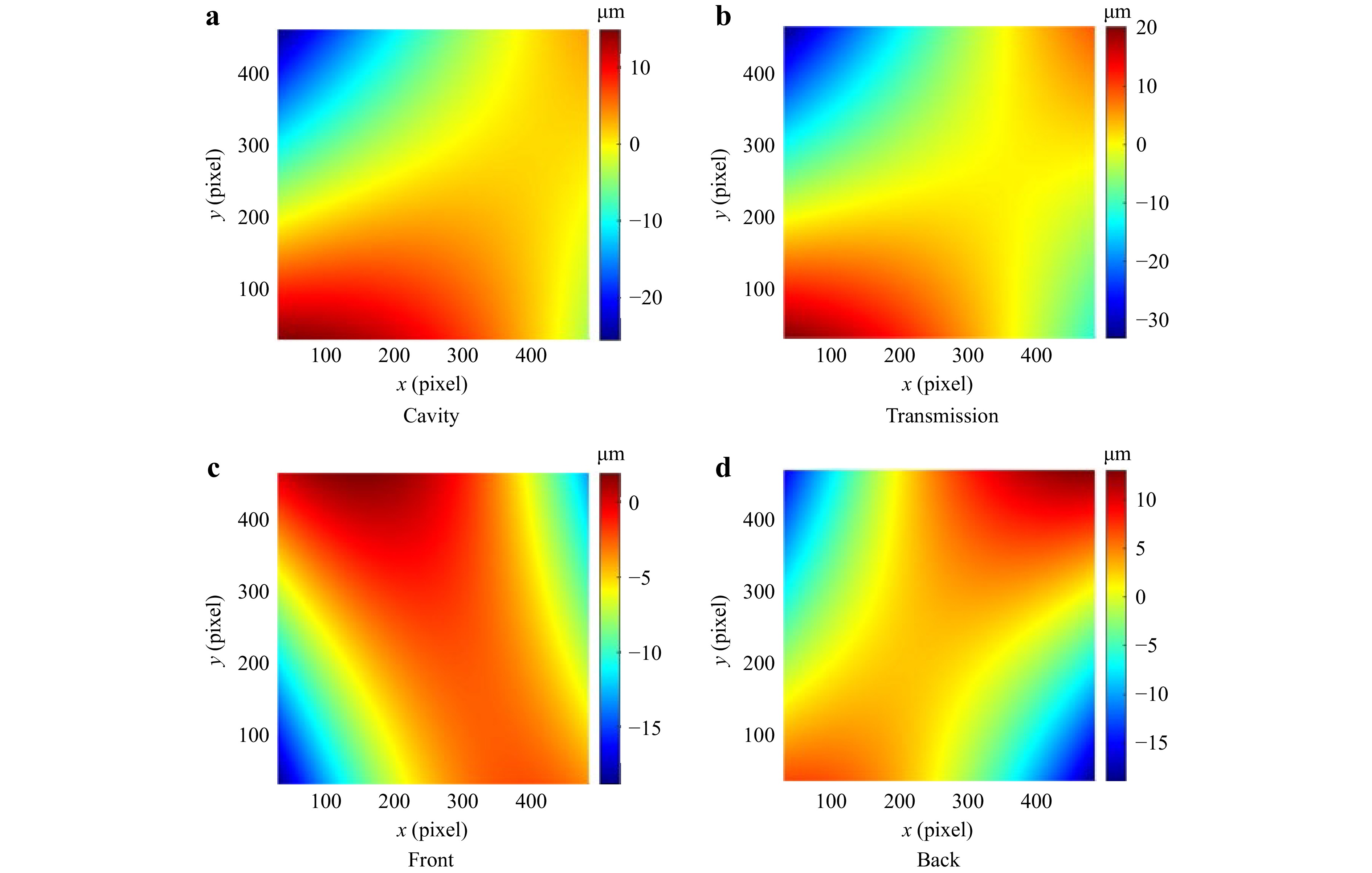
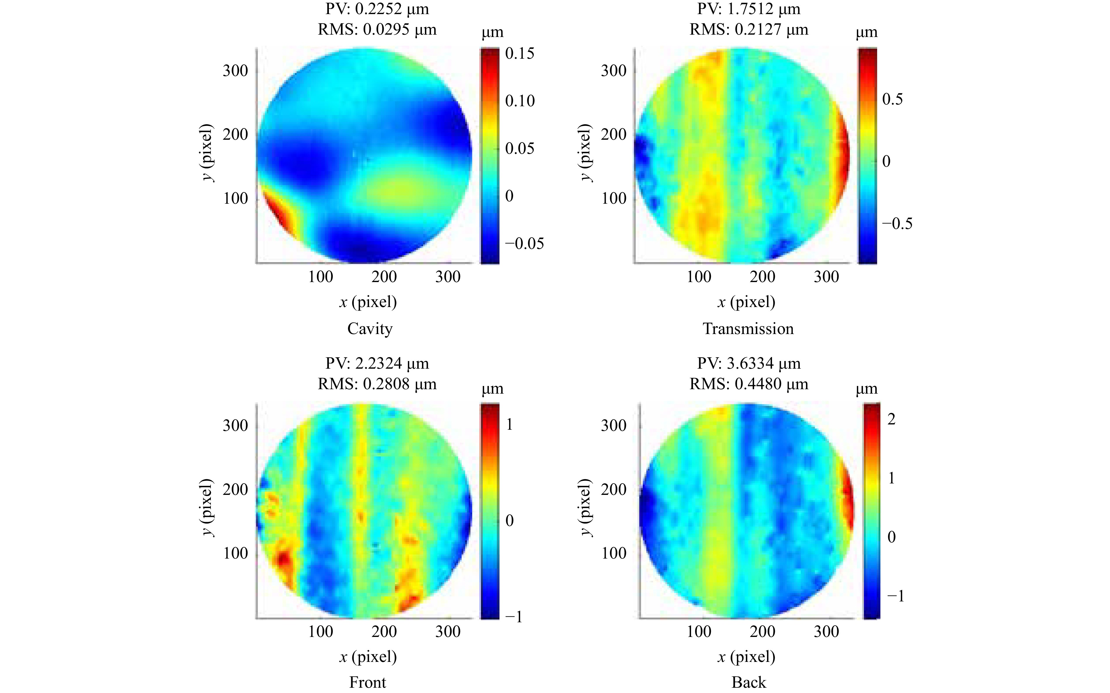
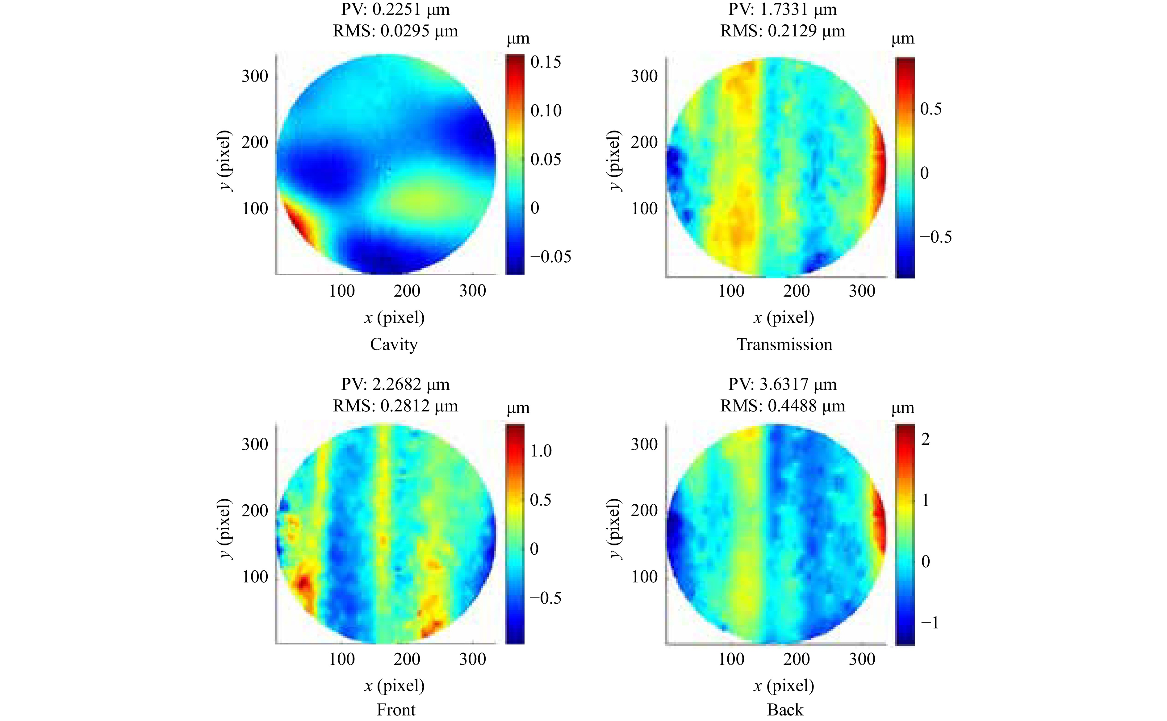
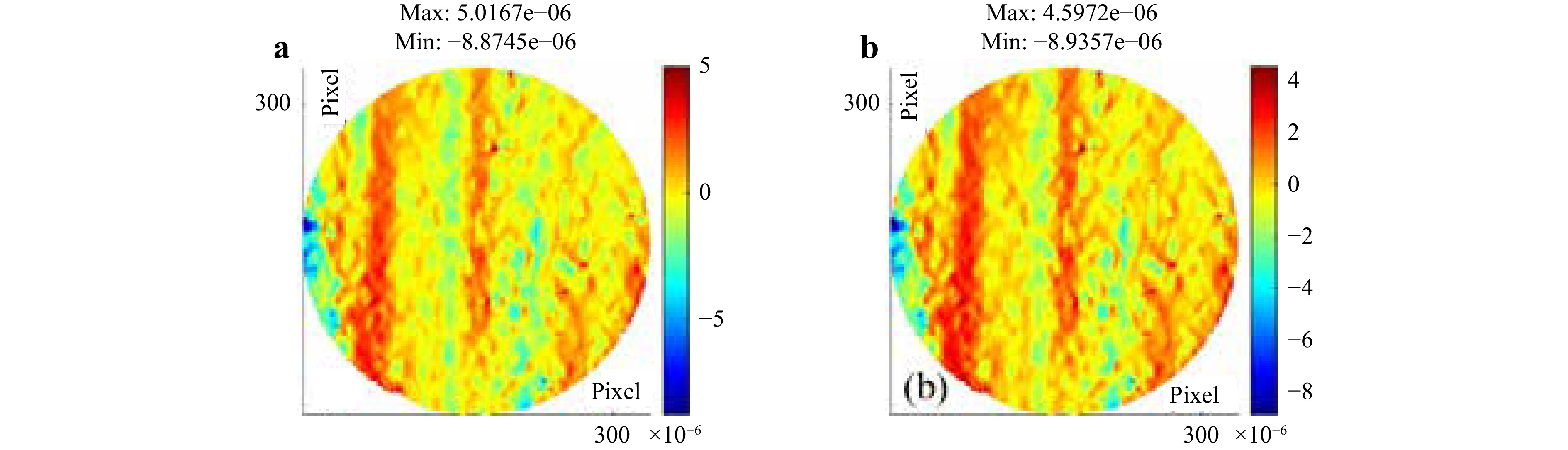
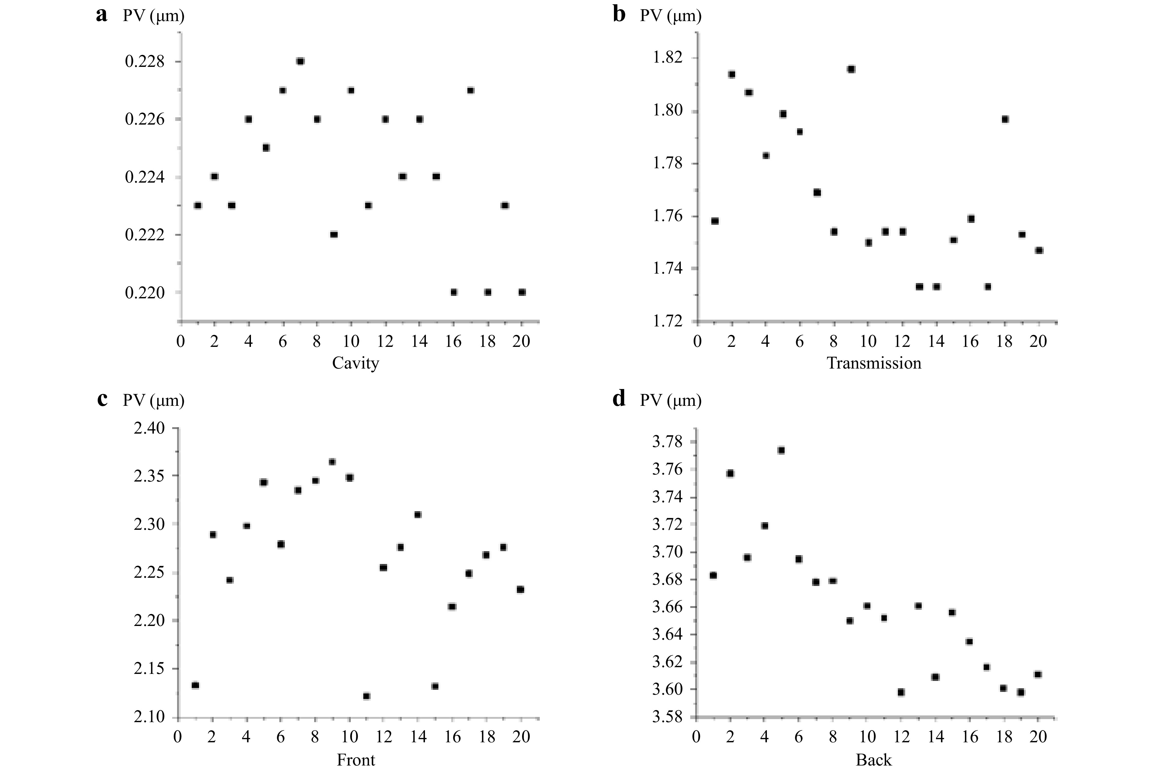
Characterizing the optical homogeneity of side-polished cylindrical transparent materials remains challenging. To address this challenge, a four-step absolute measurement method based on a Fizeau interferometer is proposed for cylindrical transparent materials. The refractive index distribution is derived from wavefront data obtained through four sequential measurements: empty-cavity interference, transmission interference, front-surface interference, and back-surface interference. A homogeneity error of 1 × 10⁻⁵ was introduced in MATLAB simulations, yielding a result of 9.9999 × 10⁻⁶ with a residual error of 8.0319 × 10⁻¹¹, confirming the method’s validity. Two repeated measurements performed at different times yielded homogeneity values of hom1 = 9.5802 × 10⁻⁶ and hom2 = 9.3331 × 10⁻⁶ (2.7% deviation), demonstrating good robustness. The uncertainties of the two measurements were 1.0997 × 10⁻⁶ and 0.8767 × 10⁻⁶, respectively, and the expanded uncertainties were 2.1994 × 10⁻⁶ and 1.7534 × 10⁻⁶, respectively. This method effectively isolates surface errors from material homogeneity, providing a practical approach for the accurate characterization of cylindrical optical components.

- First
- Prev
- 1
- 2
- 3
- 4
- 5
- 6
- 7
- 8
- 9
- 10
- Next
- Last
- Total:22
- To
- Go

 Email
Email RSS
RSS