
2025 Vol. 6, No. 2
Published. 2025, 6(2)
: 193-194
doi: 10.37188/lam.2025.028
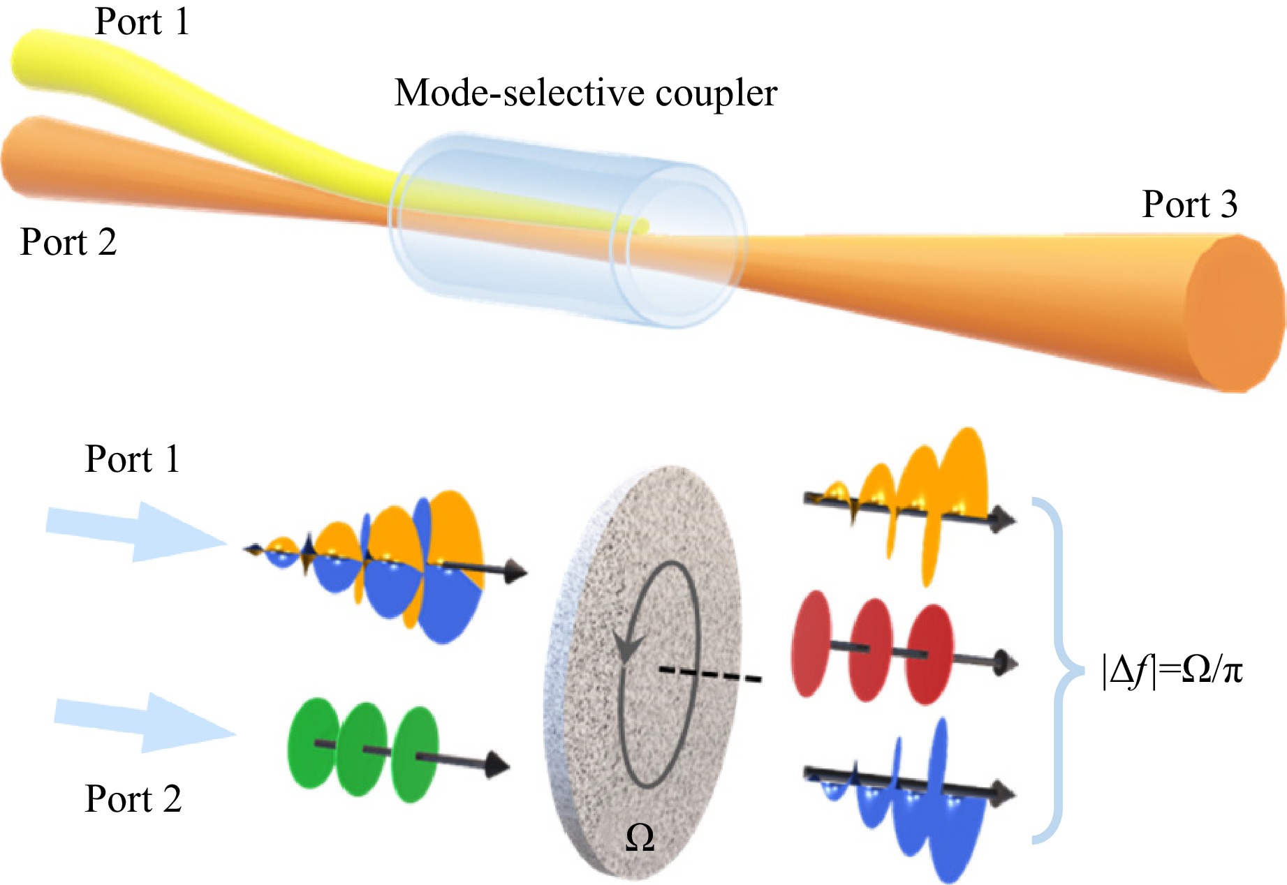
A recent breakthrough of optical metrology is the all-fiber rotational Doppler velocimetry using twisted light, which offers a compact, reciprocal, and ultra-broadband solution for measuring the angular velocity of rotating objects.

Published. 2025, 6(2)
: 195-196
doi: 10.37188/lam.2025.038
Nanoradian precision has been achieved in control of X-ray optics using feedback from optical interferometric measurements and real time adjustments of three mirrors in a simulated X-ray laser cavity in recent work reported by Koehlenbeck et al.

Published. 2025, 6(2)
: 197-200
doi: 10.37188/lam.2025.037
An advancement in the fast synthesis of lanthanide-based metal halides at room temperature is proposed and demonstrated. The reported Cs3LnCl6 scintillators are potential candidates in X-ray imaging by providing a safer, more efficient, and environmentally benign alternative to address the long-standing concerns about toxicity and fabrication complexities of existing scintillators.
Published. 2025, 6(2)
: 201-202
doi: 10.37188/lam.2025.041
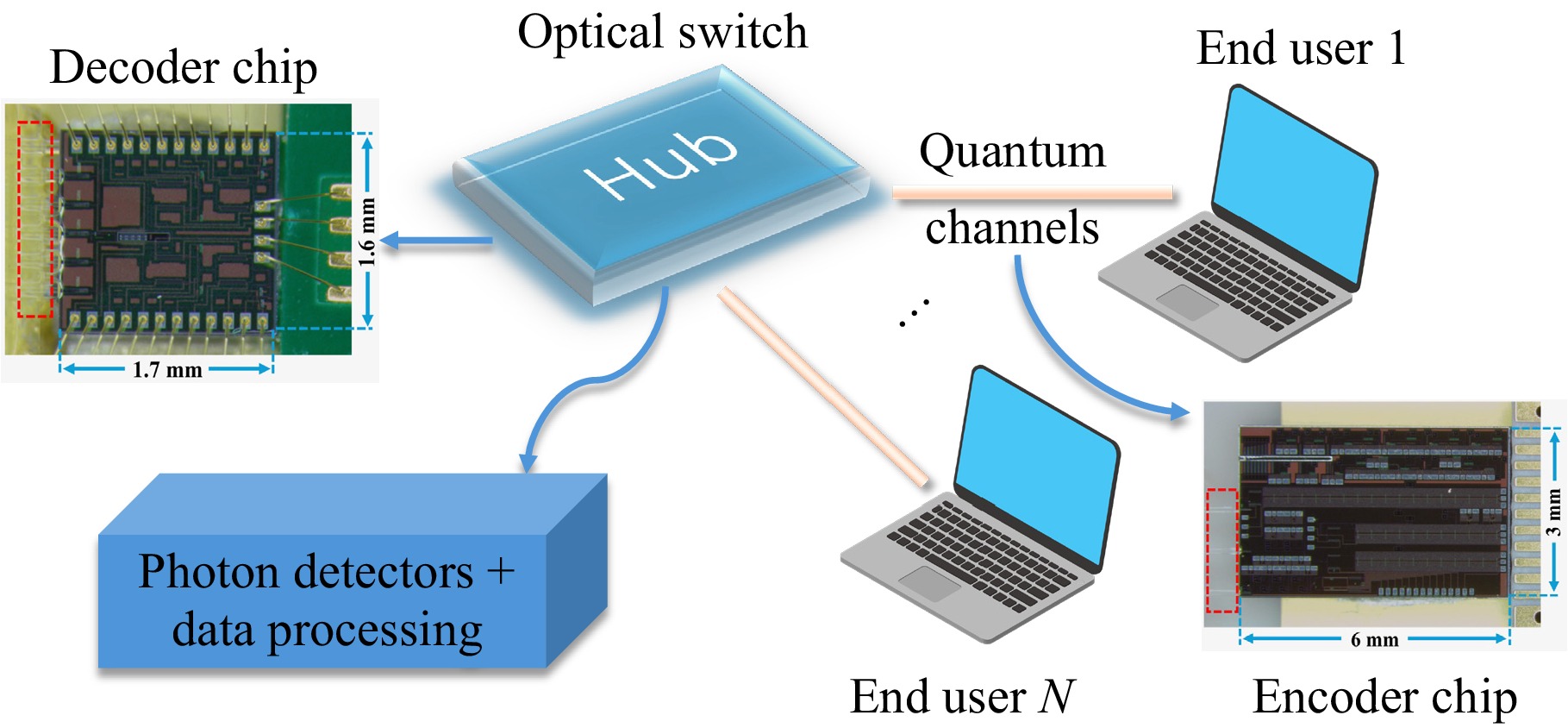
A pioneering chip-based quantum digital signature (QDS) network achieves secure document signing over 200 km of fiber, leveraging integrated photonics to miniaturize transmitters and centralize measurement systems. This breakthrough paves the way for future scalable, cost-effective, and robust quantum-secure communication networks.
Published. 2025, 6(2)
: 203-205
doi: 10.37188/lam.2025.042
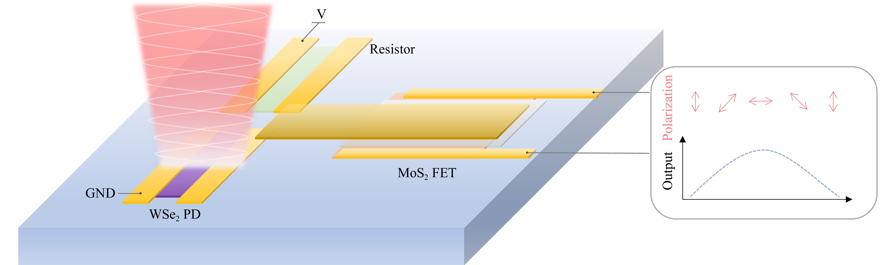
Hot carriers generated at the vicinity of the metal electrode in a WSe2 photodetector are extracted and amplified by a MoS2 field effect transistor, leading to a strong polarization-dependent photocurrent. This miniaturized polarization detection system assembled from two-dimensional materials enables new possibilities in optical communication and image recognition.
Published. 2025, 6(2)
: 206-218
doi: 10.37188/lam.2025.020
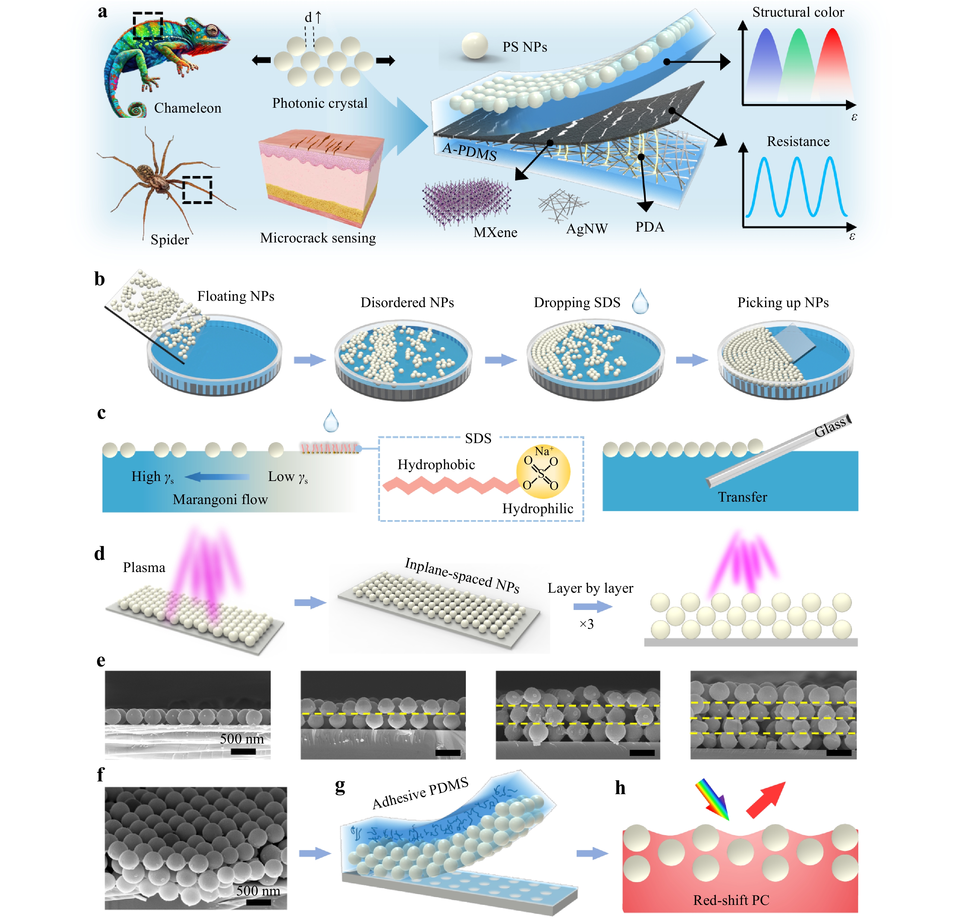
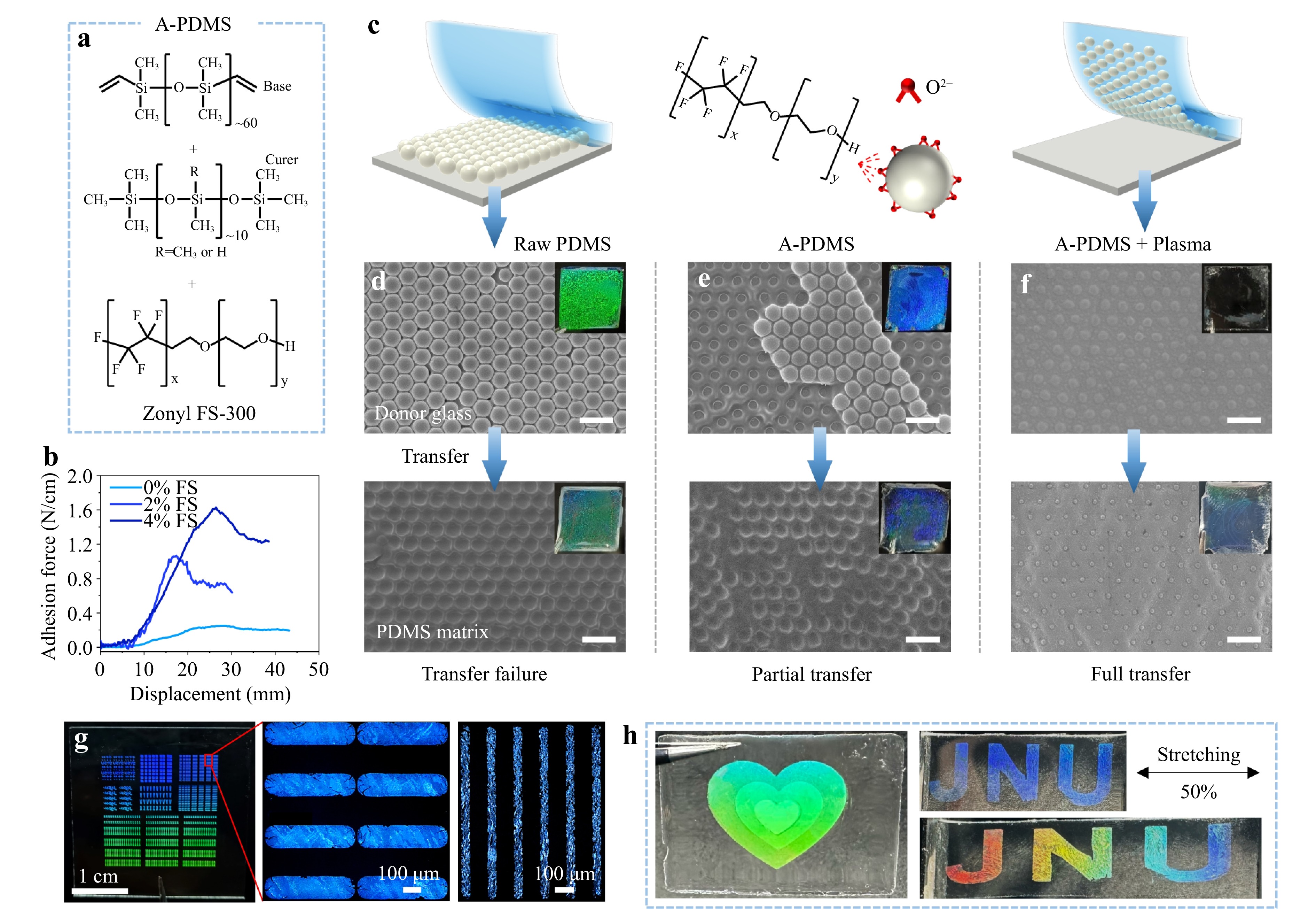
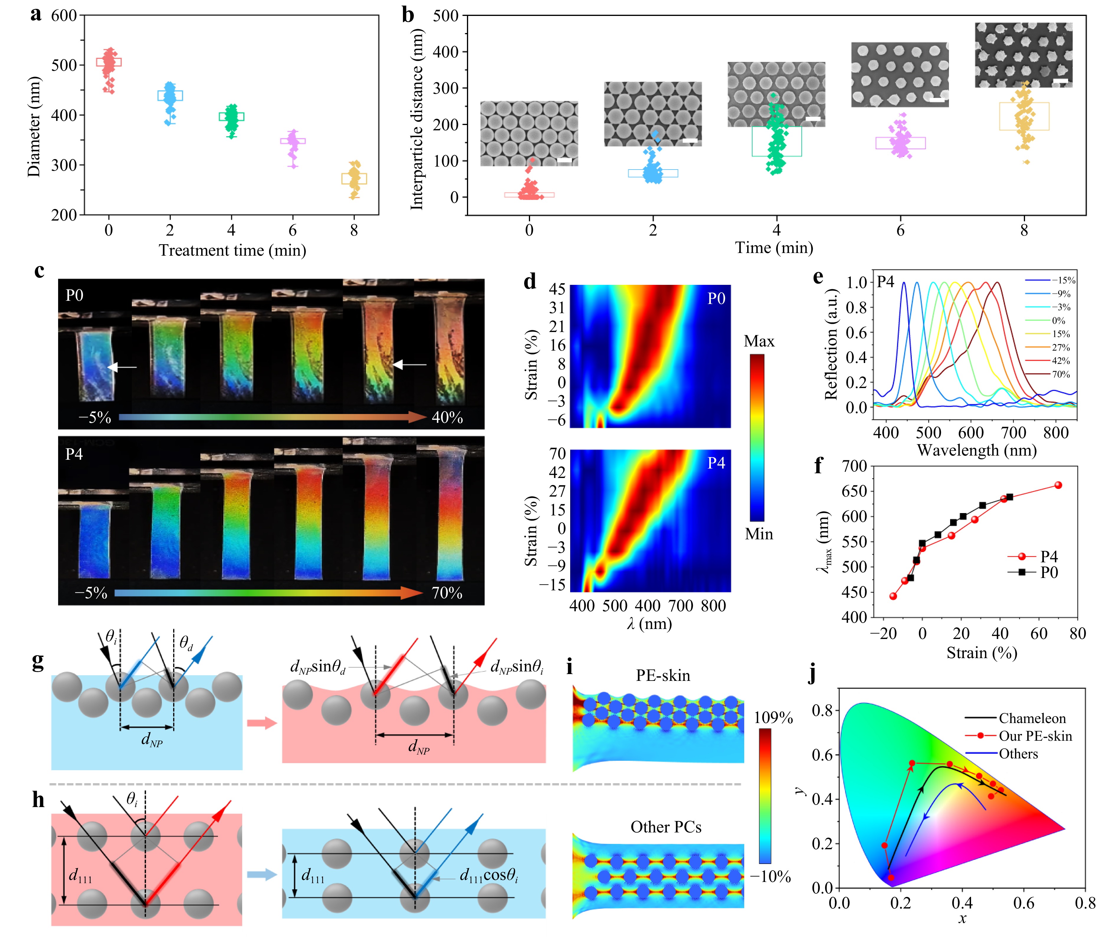
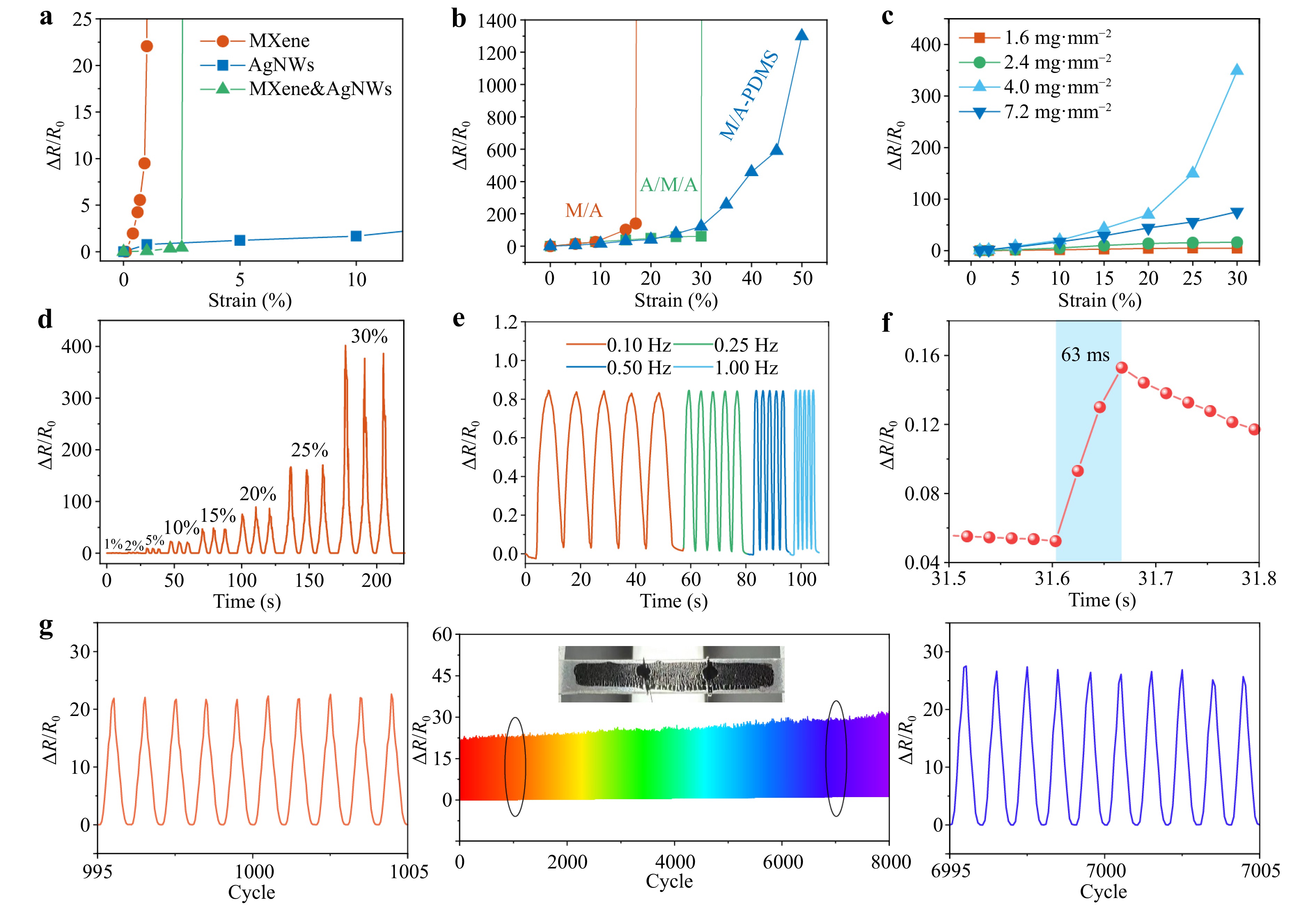
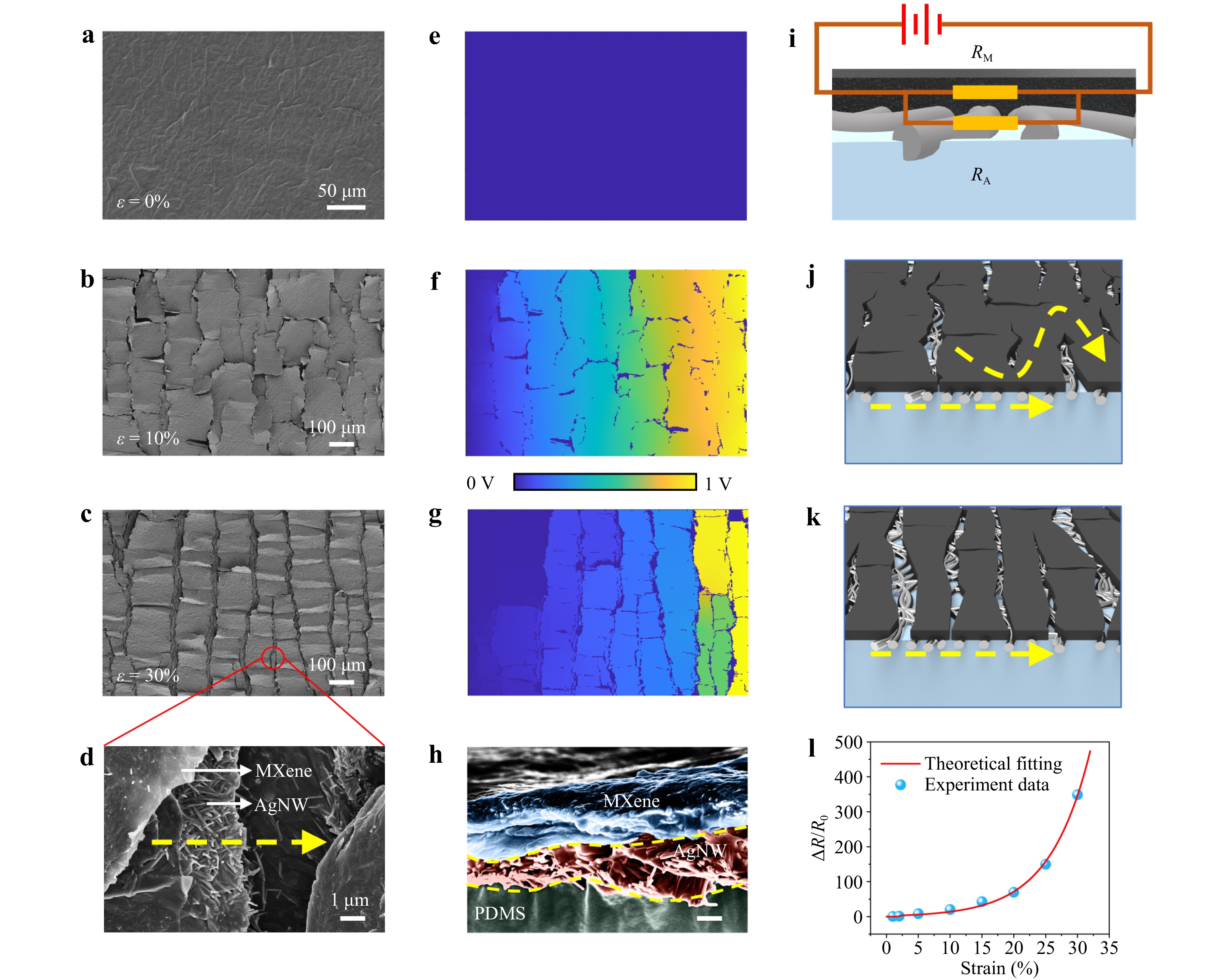
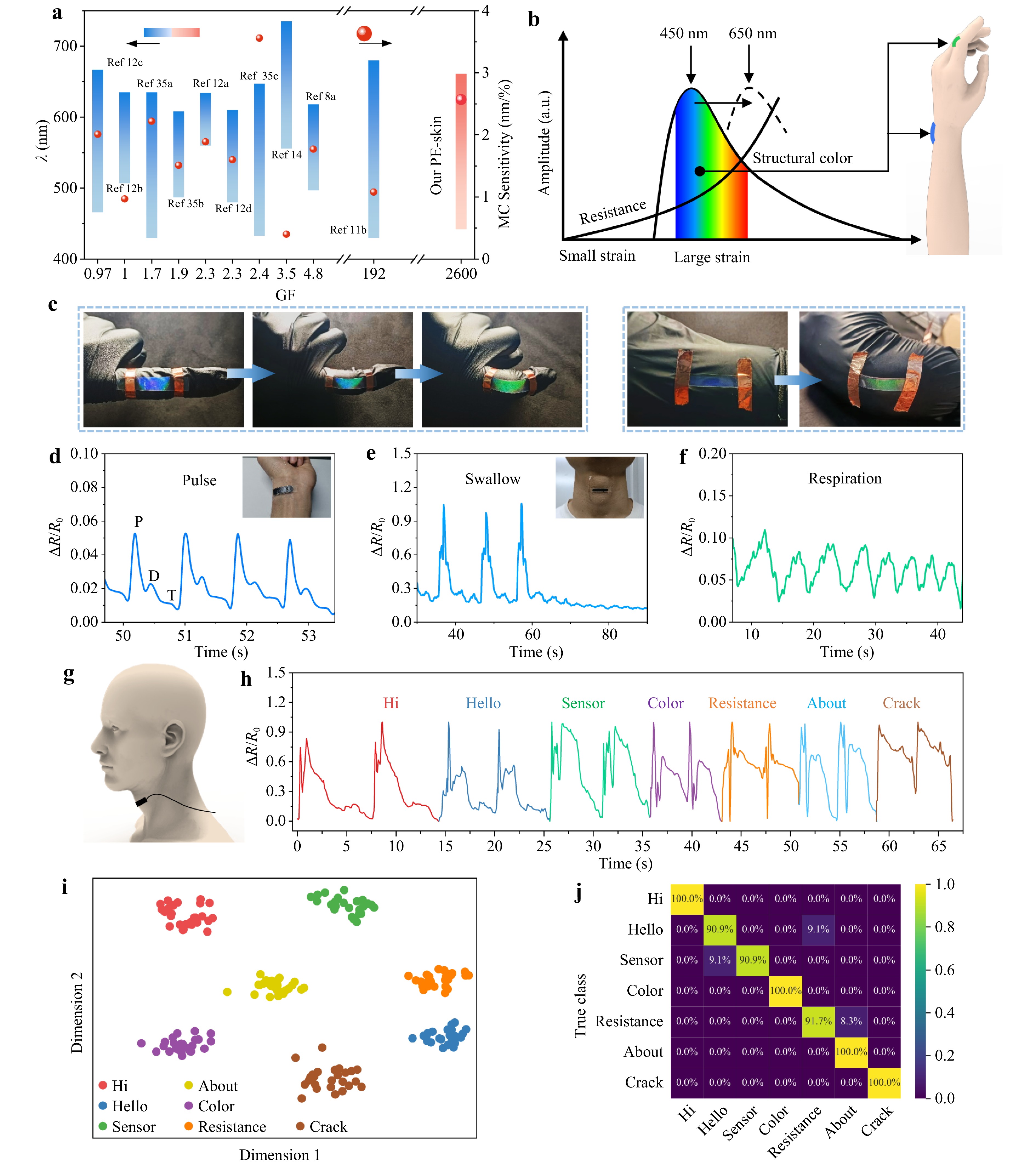
Mimicking animal skin is an effective strategy for enhancing the performance of artificial skin. Inspired by a chameleon’s iridophore and a spider’s slit organ, a novel photonic-electronic skin (PE-skin) with excellent optical/electrical dual-sensing performance was developed by integrating a photonic crystal (PC) with a conductive MXene/silver nanowire (AgNW) composite into adhesive polydimethylsiloxane. The PC layer containing in-plane-spaced and interplane-packed nanoparticle arrays was fabricated via a fast, facile, combined method of “Marangoni self-assembly”, “plasma etching”, and “adhesive PDMS transfer”. Notably, the PC exhibited a red-shift mechanochromic response through in-plane stretching, which is the first report of sharing the same mechanochromic behavior as a chameleon iridophore. The underlying MXene layer formed slit-organ-like cracks that provided high sensitivity, whereas the AgNWs maintained their conductivity under large strains. The resultant PE-skin exhibited a high mechanochromic sensitivity (2.57 nm %−1) and a high electrical gauge factor of 2600 in a large strain-sensing range (up to 85%). These advantages have been confirmed in the detection of full-range human motions, such as speech recognition, using a deep neural network algorithm. The red-shift stretchable PC demonstrates a new paradigm for artificial chameleon skins, and the bionic PC crack bilayer structure extends the design concept for visually interactive e-skins.
Published. 2025, 6(2)
: 219-227
doi: 10.37188/lam.2025.003
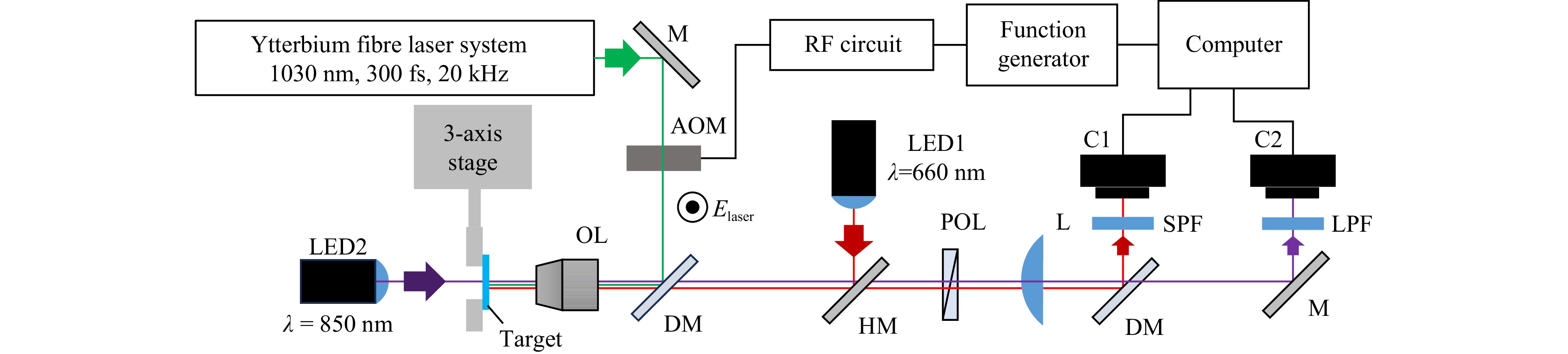
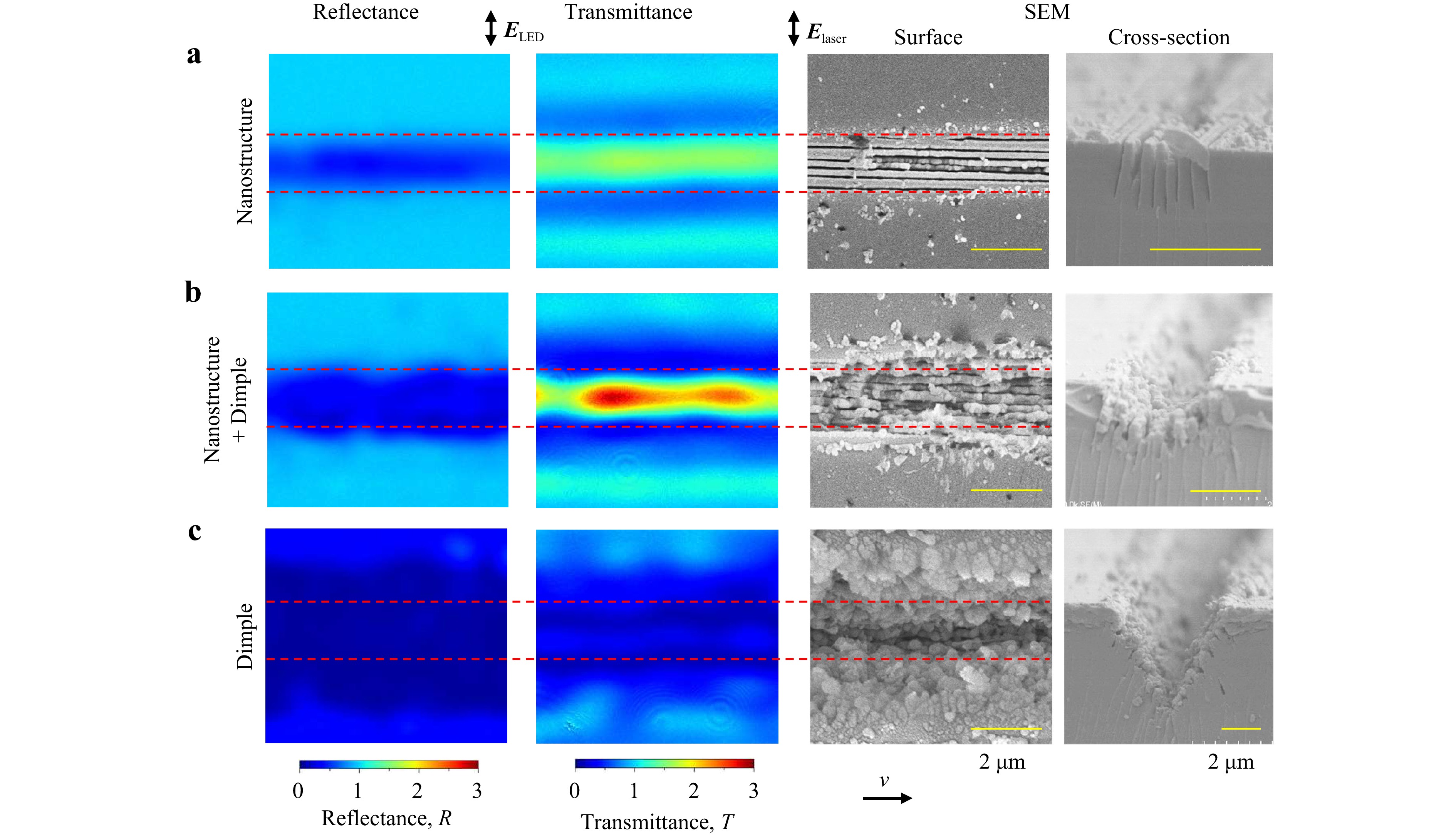
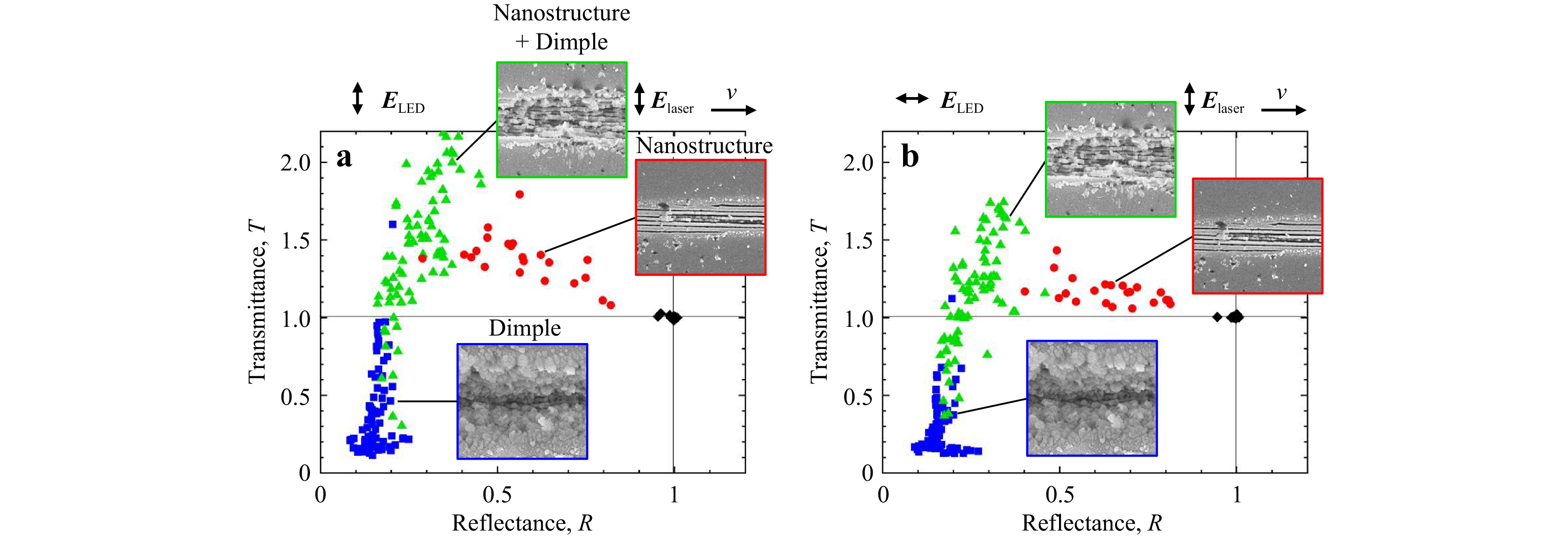
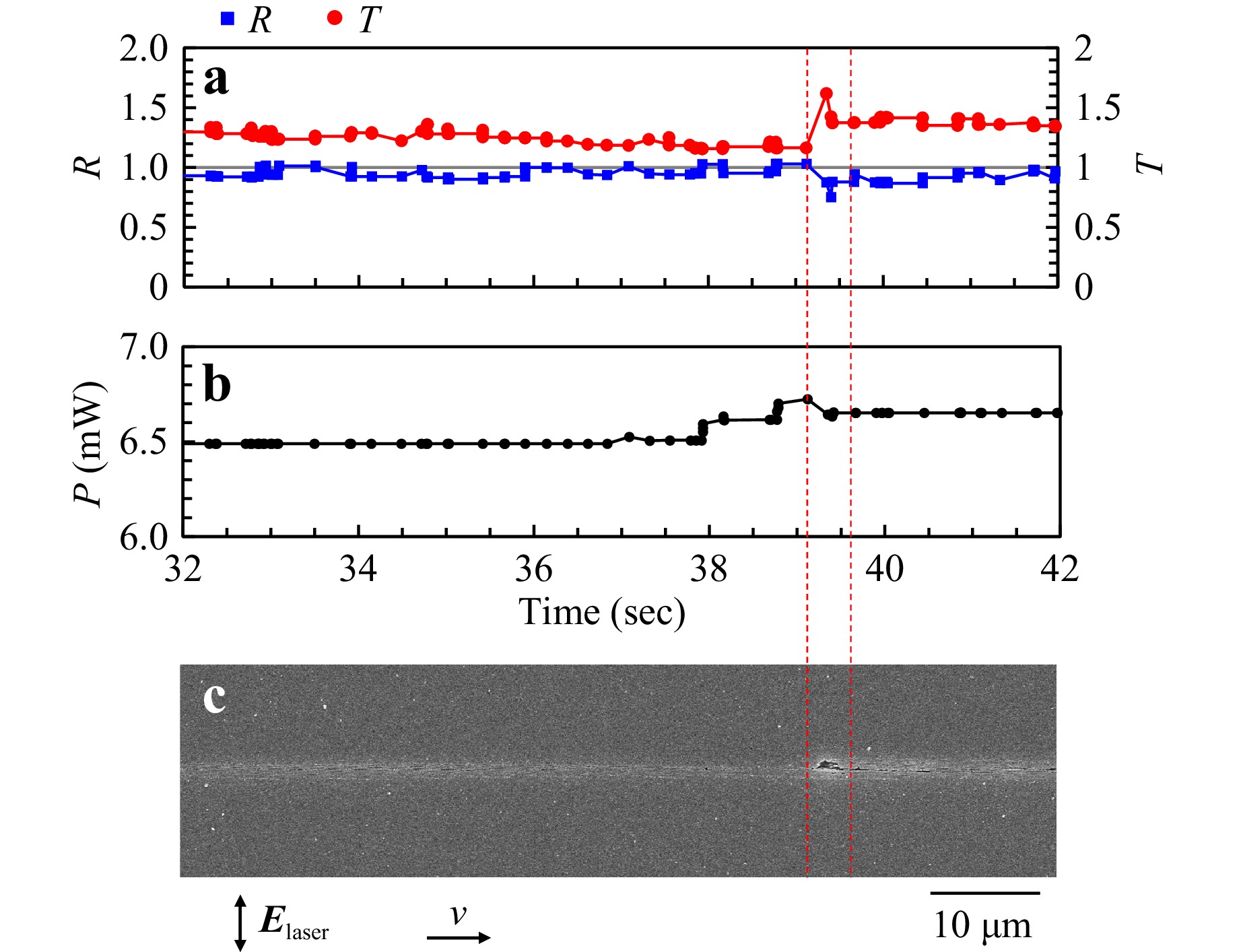
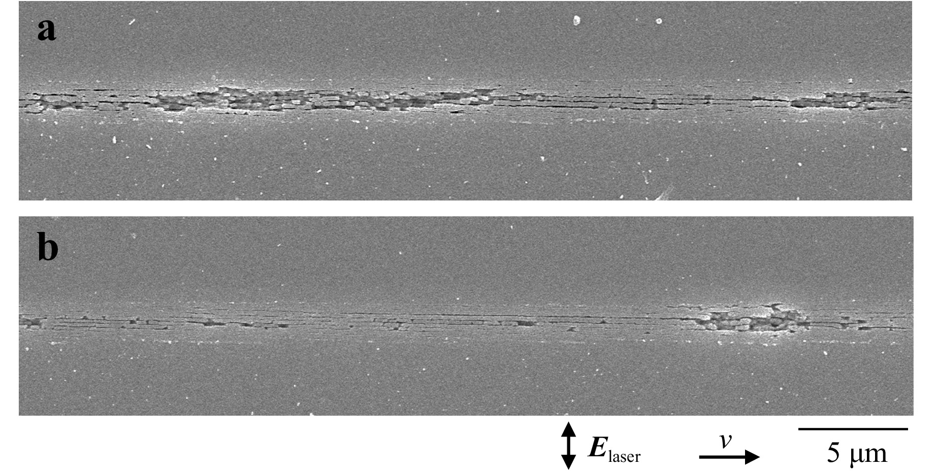
Femtosecond laser pulses can be employed to directly form periodic nanostructures on solid surfaces, including hard materials such as diamond and sapphire, via ablation. Thus, this technique is promising for industrial nanofabrication applications. However, the stable formation of uniform nanostructures is challenging because of their high sensitivity to changes in processing conditions, such as the surface roughness of materials and laser power. Herein, we report a real-time monitoring and control approach for fabricating high-quality nanostructures on glass surfaces. We measured the reflectance and transmittance of a laser-irradiated surface simultaneously and determined their specific values corresponding to the formation of a uniform nanostructure with a period of 200 nm and depth of 1 μm. By utilising these values as feedback signals in a proportional-integral-derivative control system, we adjusted the laser power during irradiation to form a uniform nanostructure. This approach led to a significant reduction in the defect ratio of the nanostructure (~2.4%), which represents a 10-fold reduction compared with uncontrolled processing. Our results demonstrate the potential for the stable and direct fabrication of high-quality nanostructures on solids and offer a valuable method for the quality assurance of nanostructures for various applications.
Published. 2025, 6(2)
: 228-235
doi: 10.37188/lam.2025.015
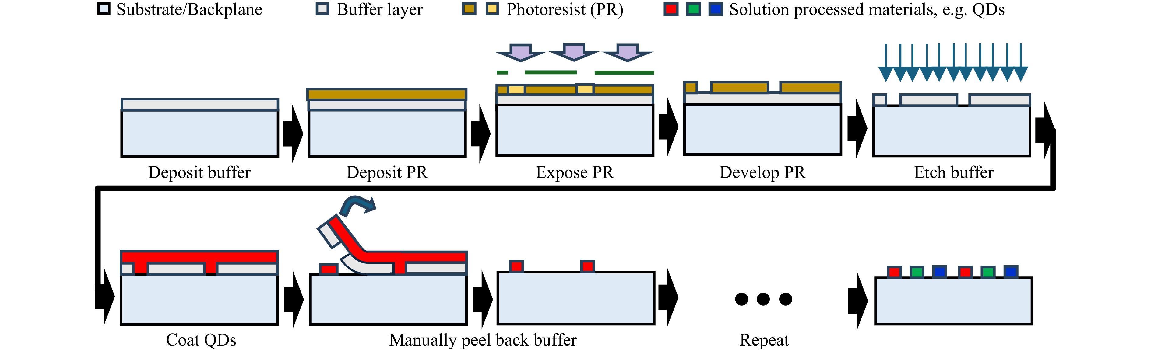
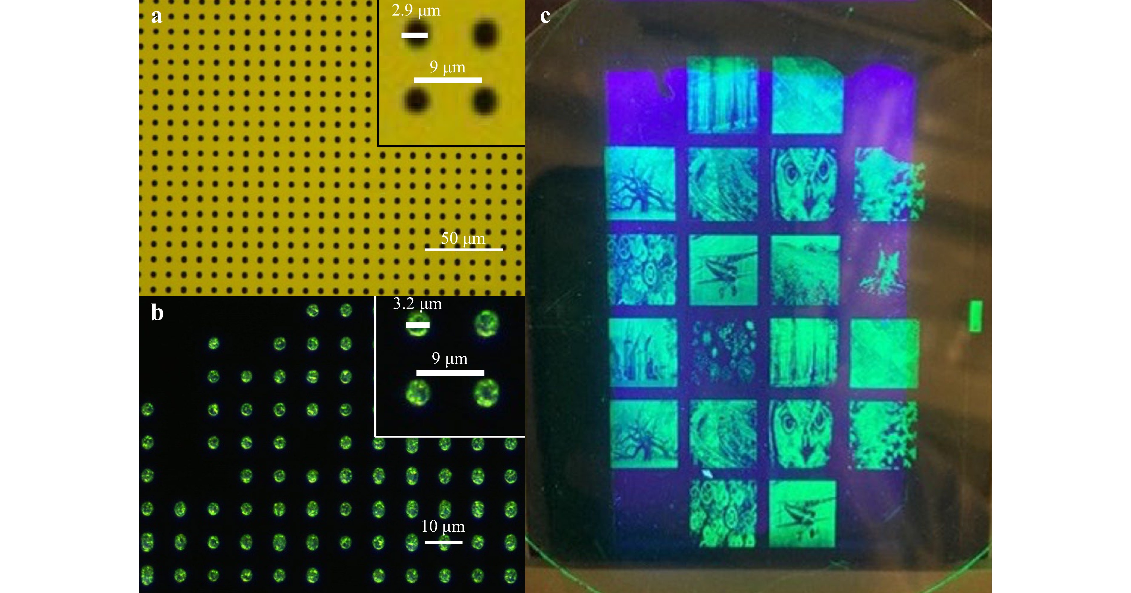
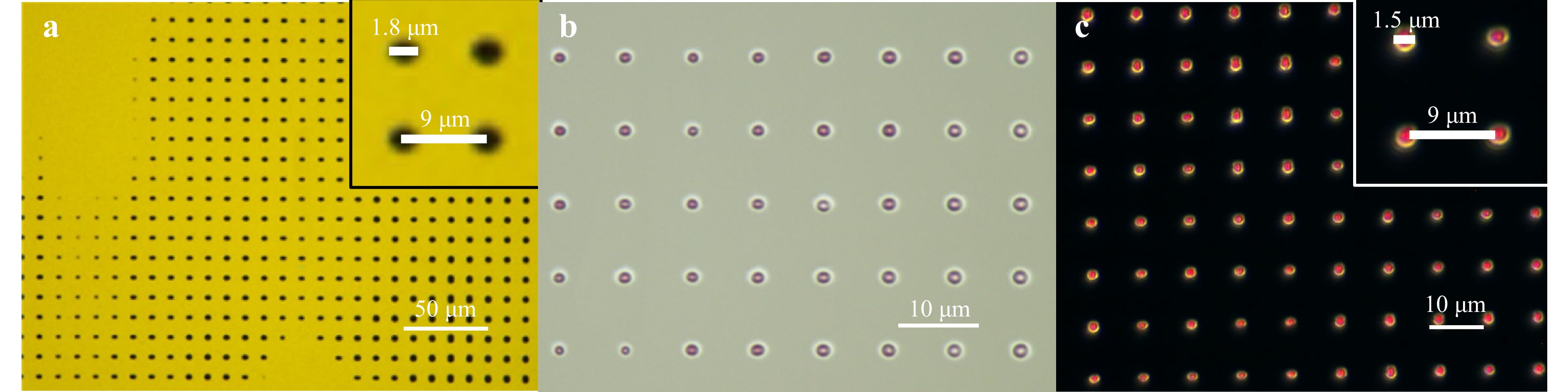
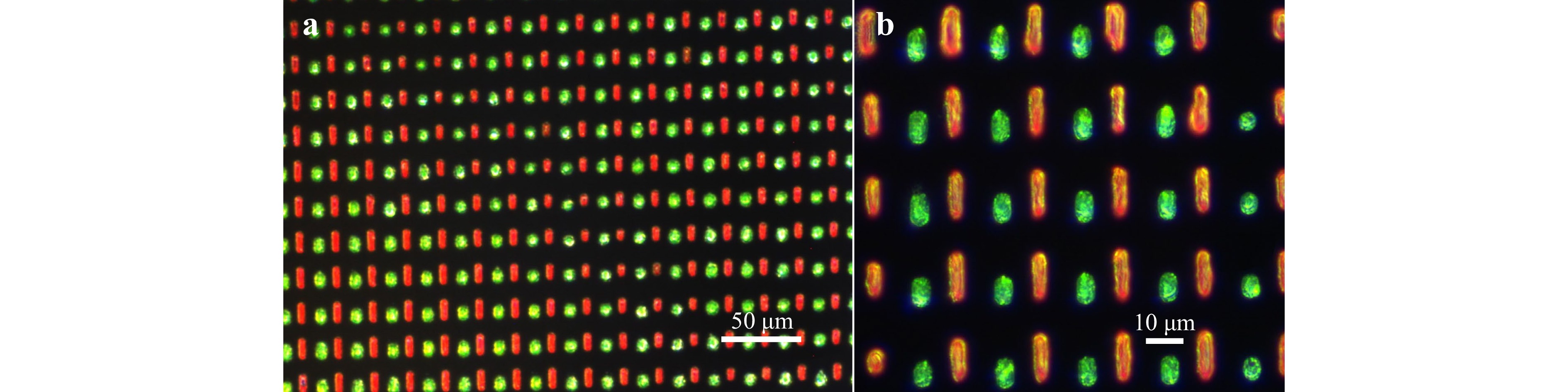
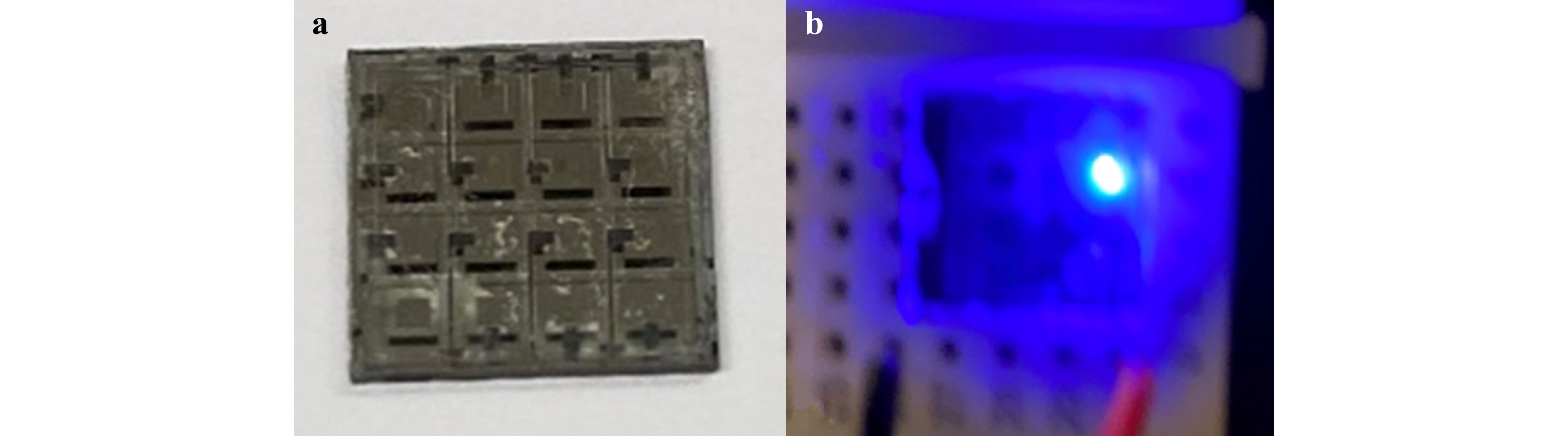
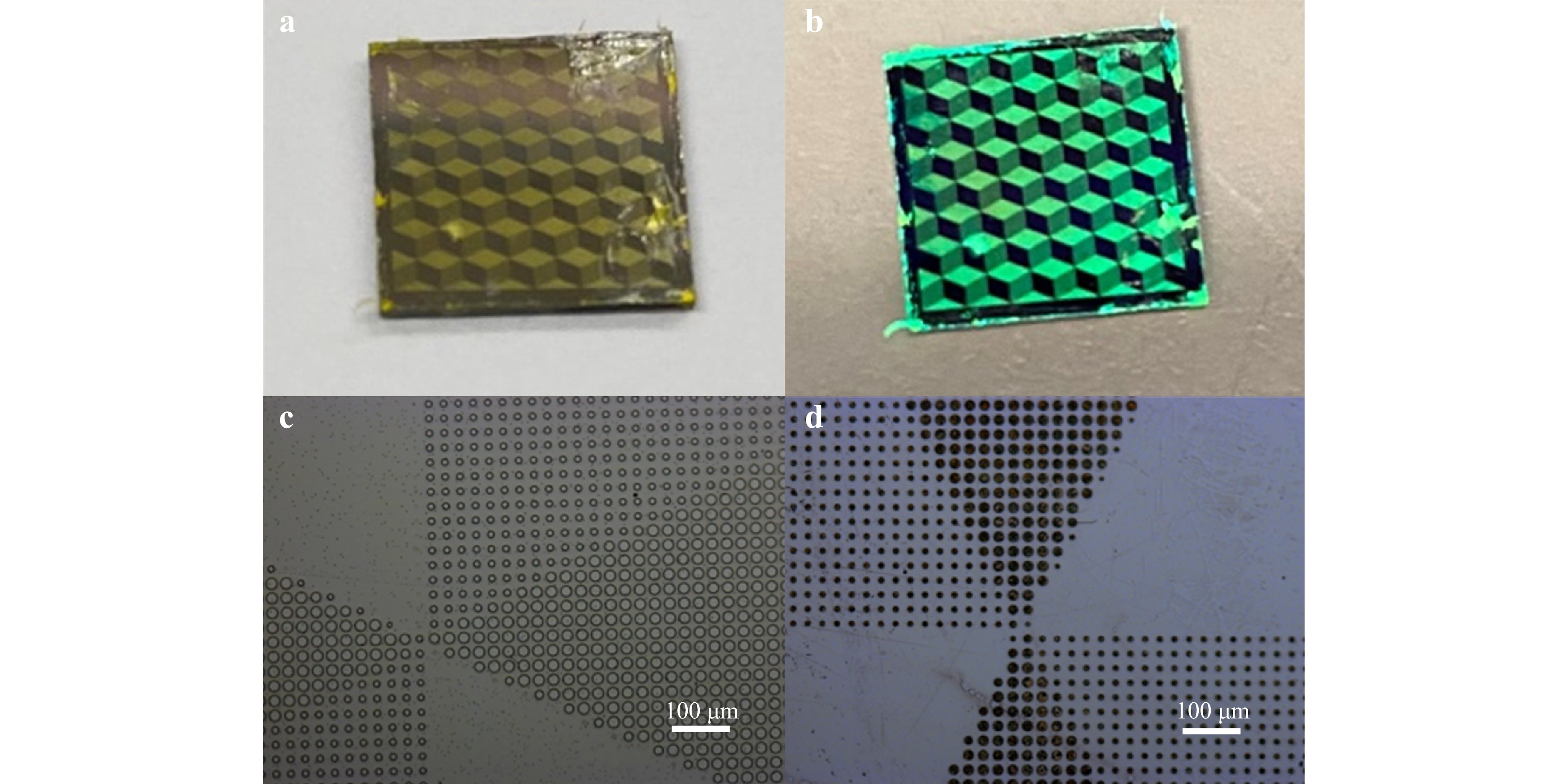
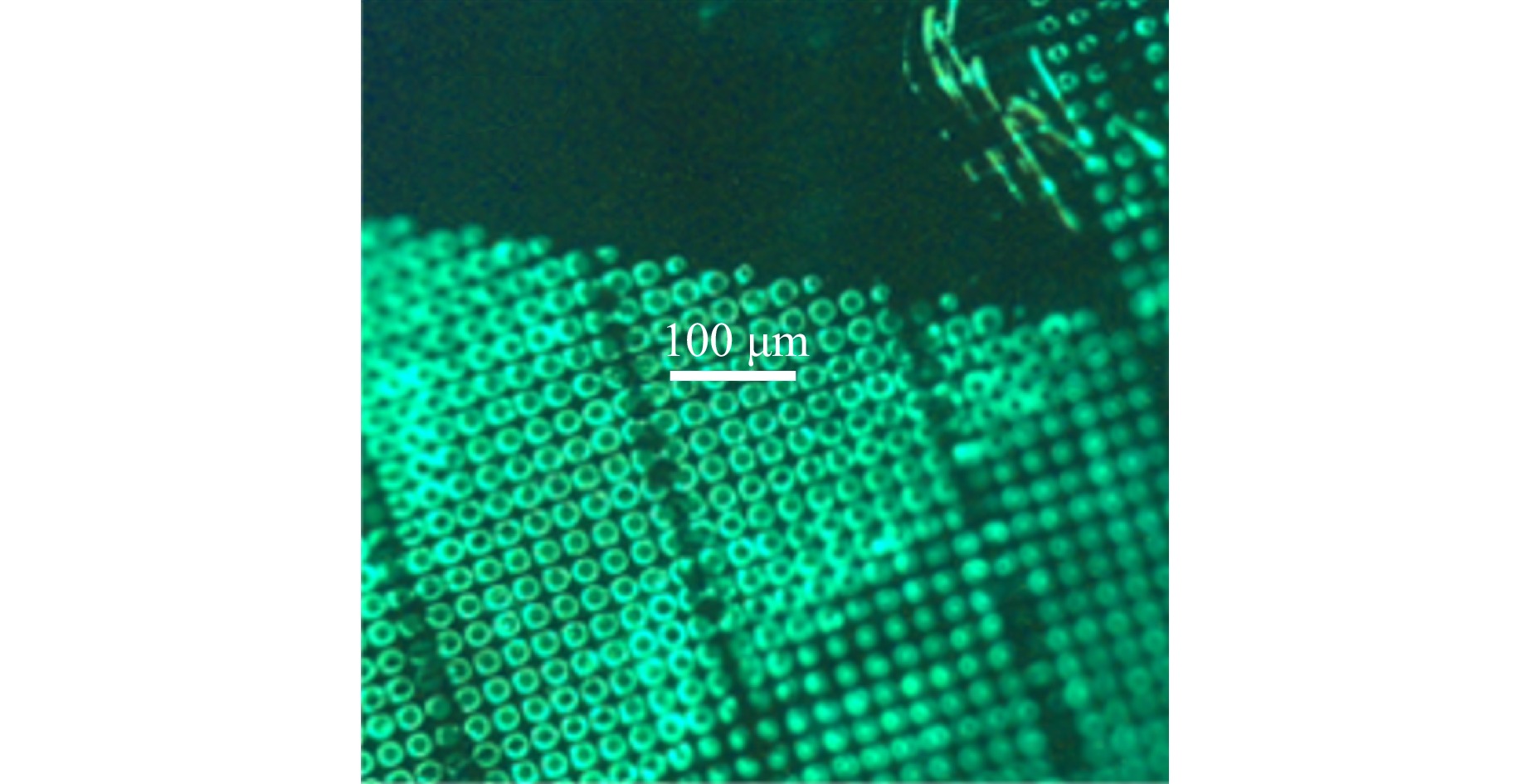
A universal method of micro-patterning thin quantum dot films is highly desired by industry to enable the integration of quantum dot materials with optoelectronic devices. Many of the methods reported so far, including specially engineered photoresist or ink-jet printing, are either of poor yield, resolution limited, difficult to scale for mass production, overly expensive, or sacrificing some optical quality of the quantum dots. In our previous work, we presented a dry photolithographic lift-off method for pixelization of solution-processed materials and demonstrated its application in patterning perovskite quantum dot pixels, 10 µm in diameter, to construct a static micro-display. This report presents further development of this method and demonstrates high-resolution patterning (~1 µm diameter), full-scale processing on a 100 mm wafer, and multi-color integration of two different varieties of quantum dots. Perovskite and cadmium-selenide quantum dots were adopted for the experimentation, but the method can be applied to other types of solution-processed materials. We also demonstrate the viability of this method for constructing high-resolution micro-arrays of quantum dot color-convertors by fabricating patterned films directly on top of a blue gallium-nitride LED substrate. The green perovskite quantum dots used for fabrication were synthesized via the room-temperature ligand-assisted reprecipitation method developed by our research group, yielding a photoluminescent quantum yield of 93.6% and full-width half-maximum emission linewidth less than 20 nm. Our results demonstrate the viability of this method for use in scalable manufacturing of high-resolution micro-displays paving the way for improved optoelectronic applications.
Published. 2025, 6(2)
: 236-247
doi: 10.37188/lam.2025.017
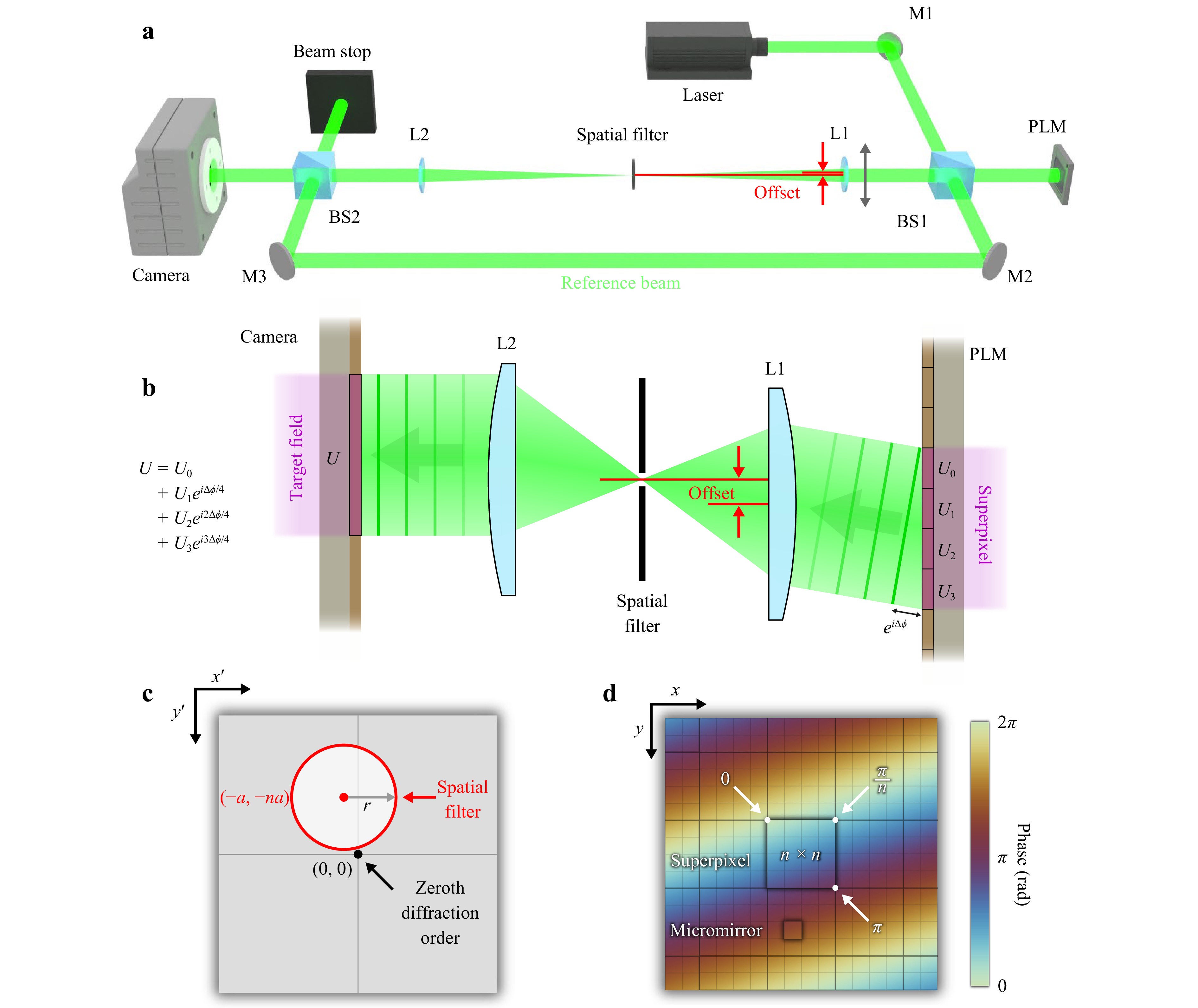
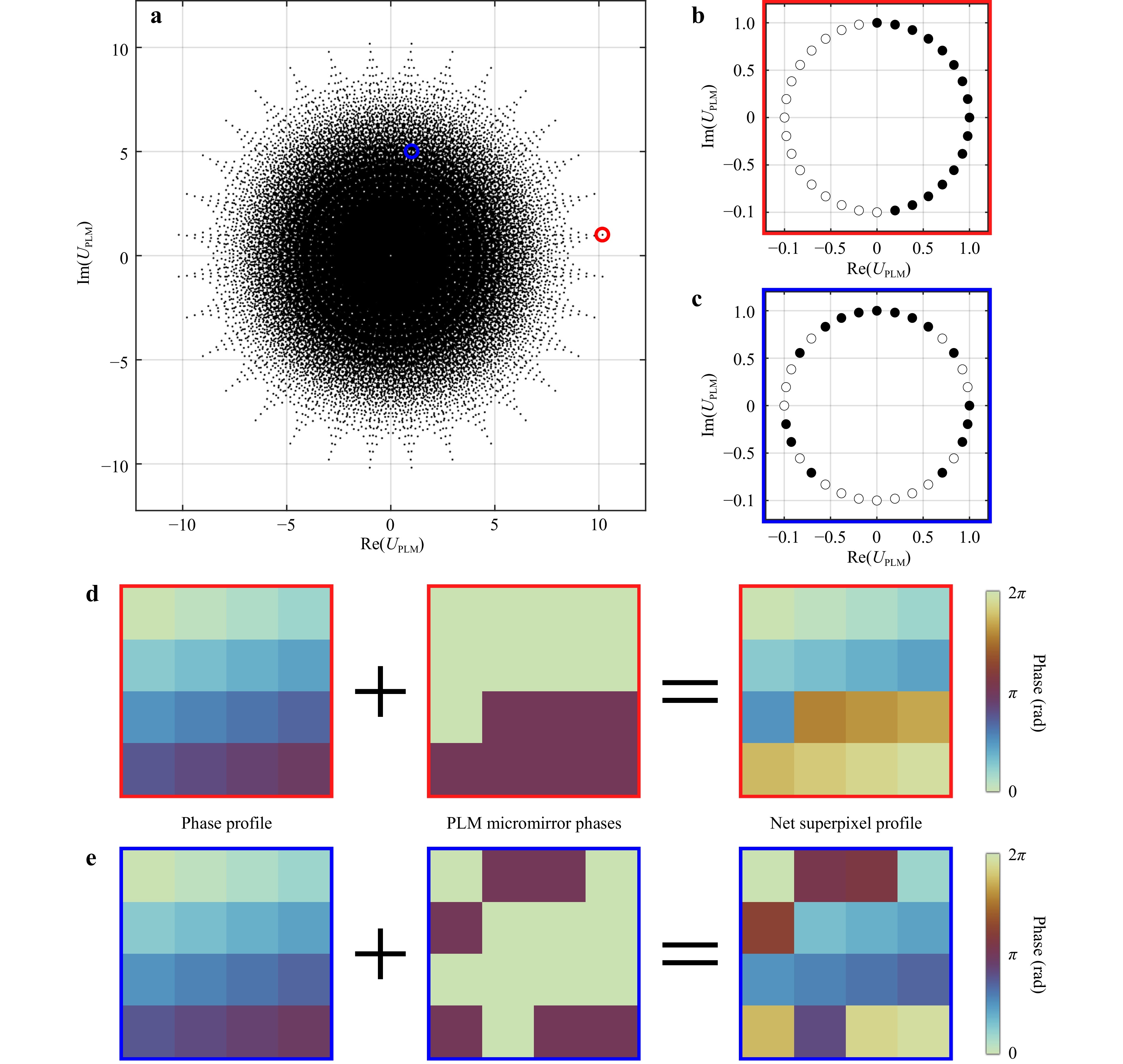
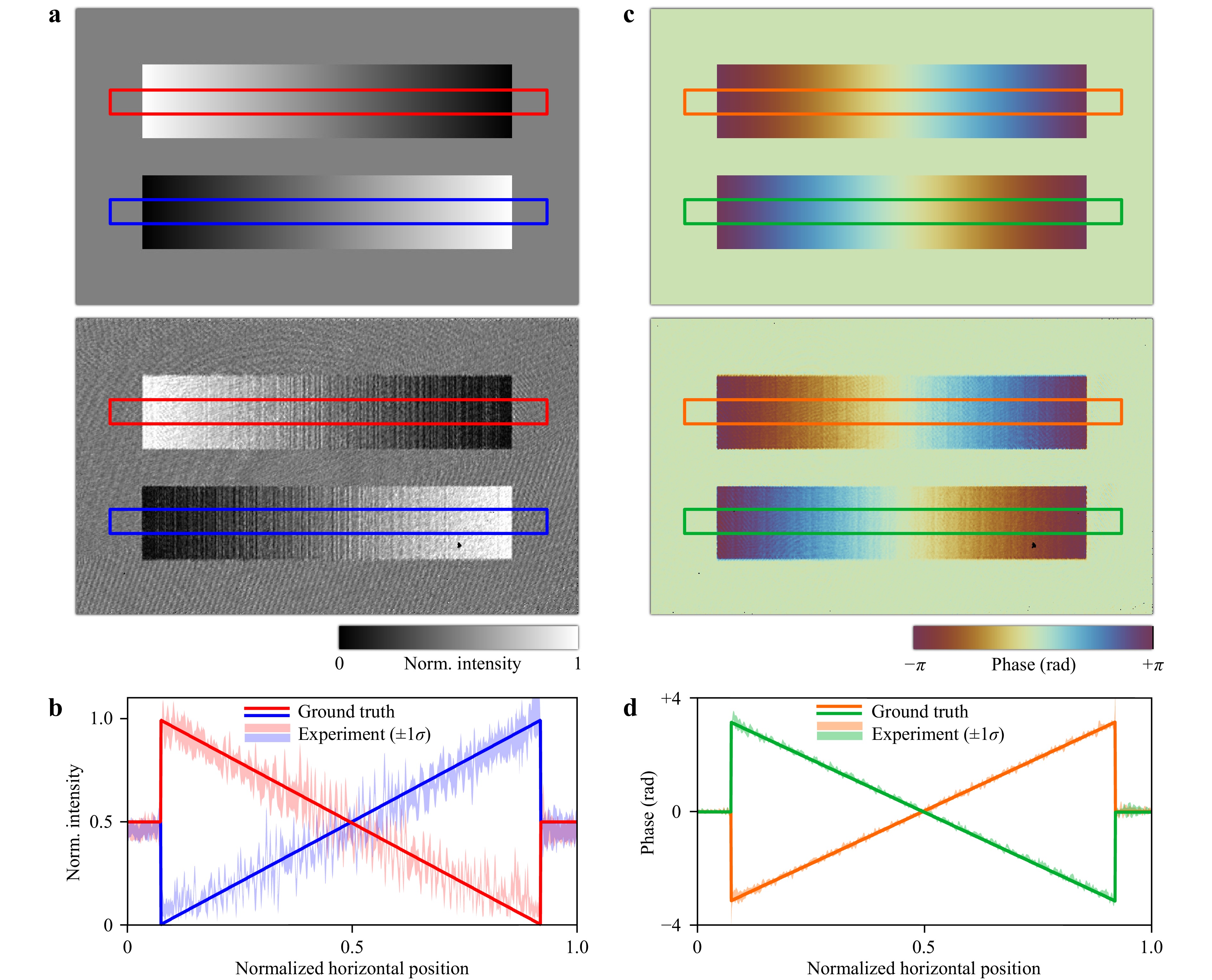
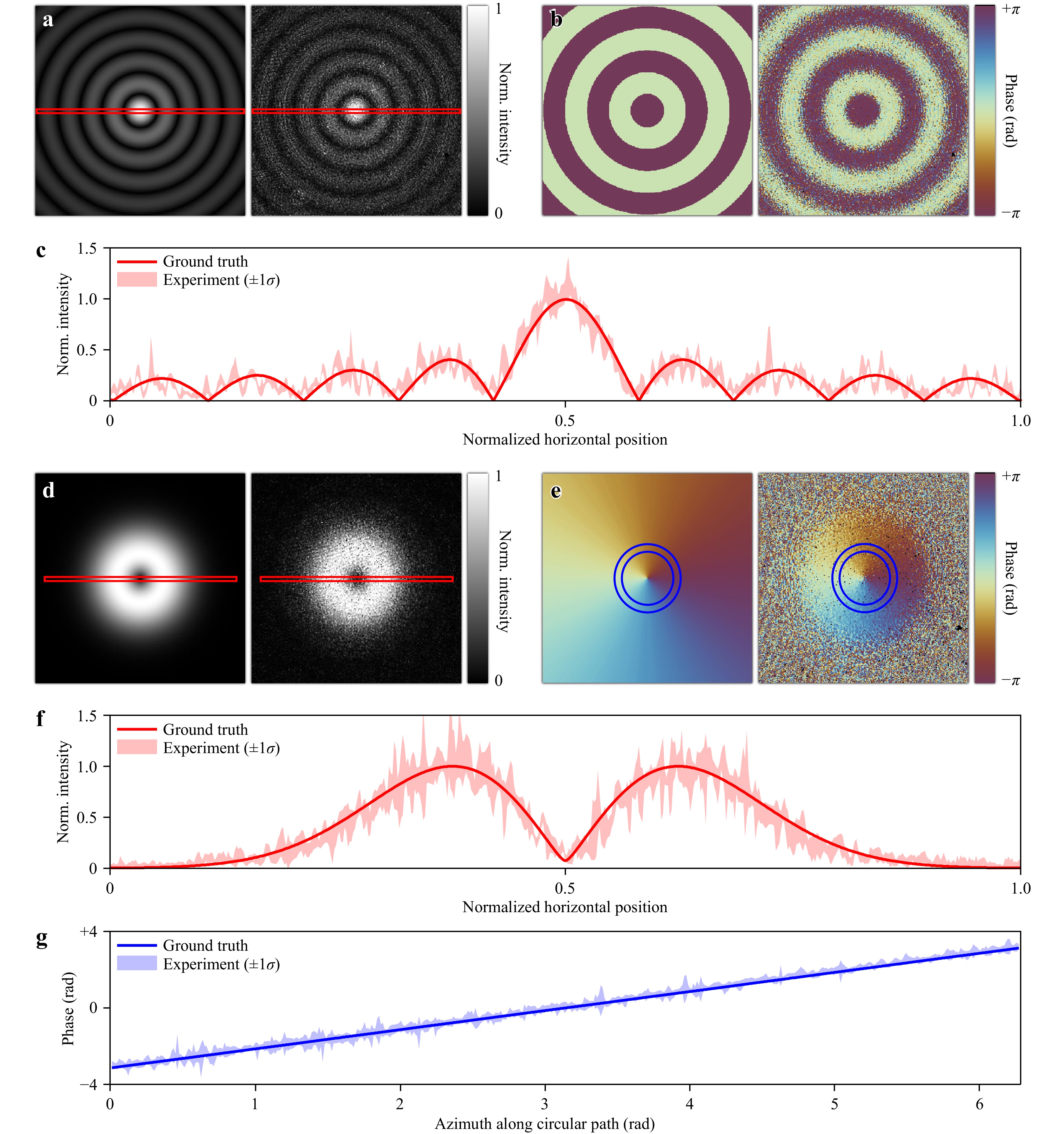
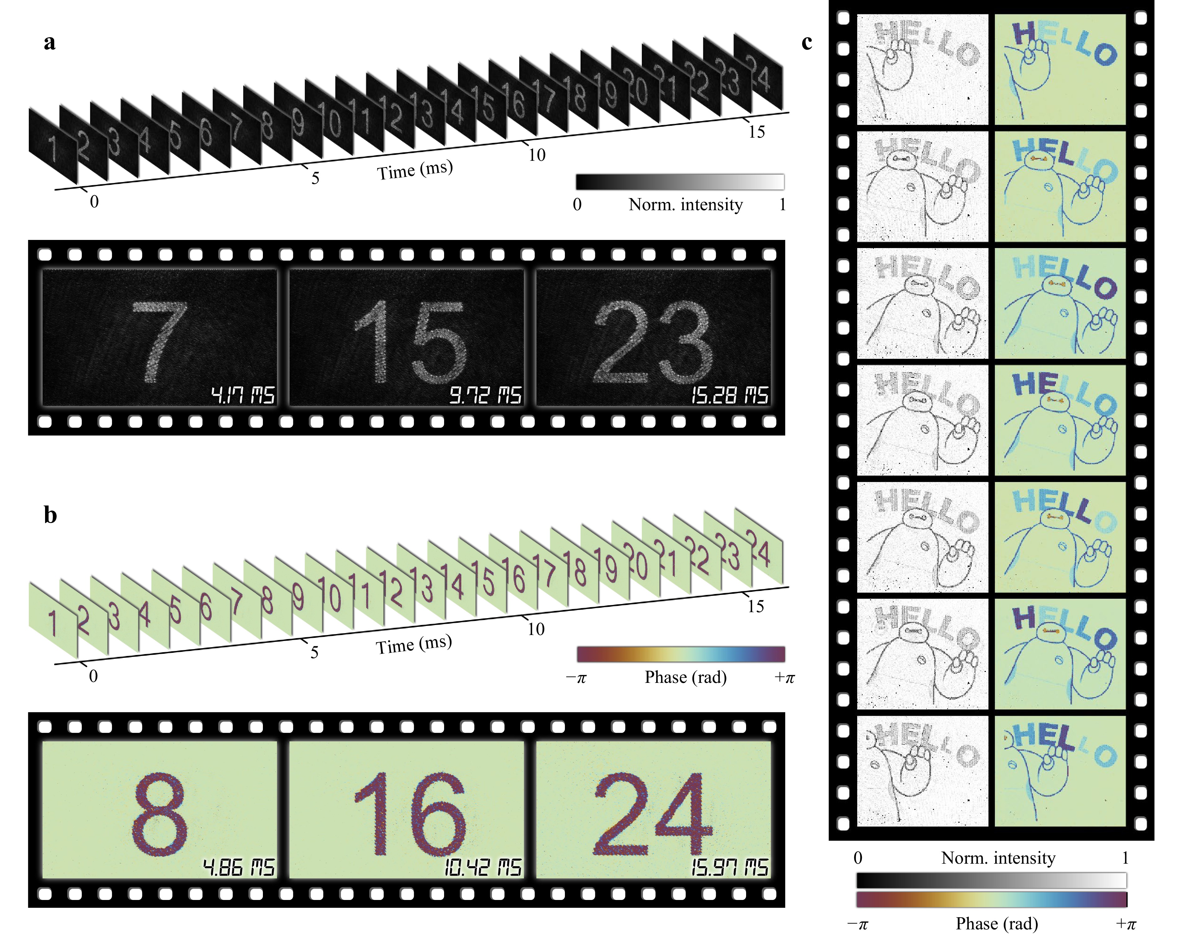
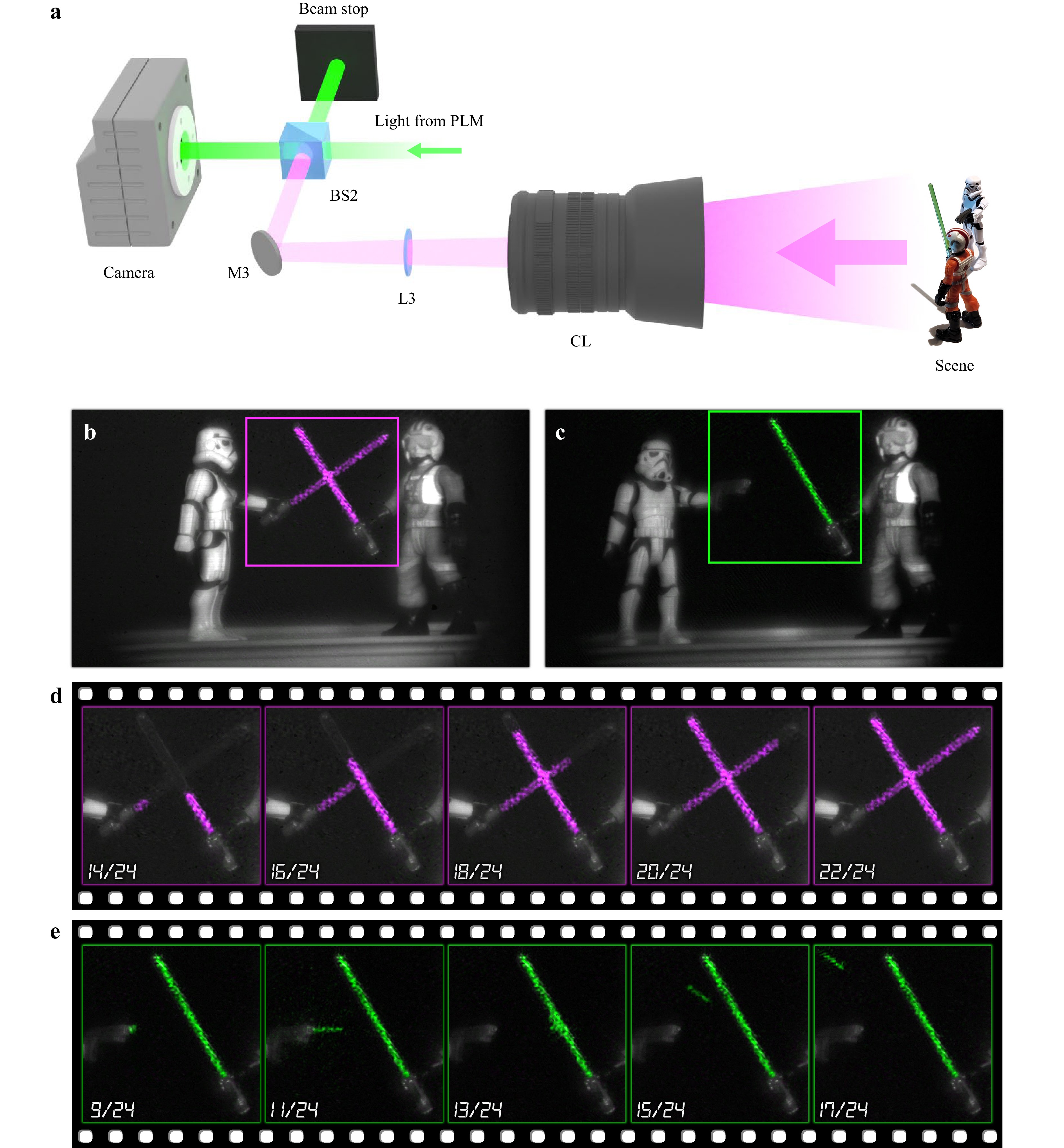
Complex field modulation (CFM) has found a plethora of applications in physics, biomedicine, and instrumentation. Among existing methods, superpixel-based CFM has been increasingly featured because of its advantages in high modulation accuracy and its compatibility with high-speed spatial light modulators (SLMs). Nonetheless, the mainstream approach based on binary-amplitude modulation confronts limitations in optical efficiency and dynamic range. To surmount these challenges, we develop binary phase-engraved (BiPE) superpixel-based CFM and implement it using the phase light modulator (PLM)—a new micro-electromechanical system-based SLM undergoing development by Texas Instruments in recent years. Using BiPE superpixels, we demonstrate high-accuracy spatial amplitude and phase modulation at up to 1.44 kHz. To showcase its broad utility, we apply BiPE-superpixel-based CFM to beam shaping, high-speed projection, and augmented-reality display.
Published. 2025, 6(2)
: 248-259
doi: 10.37188/lam.2025.021
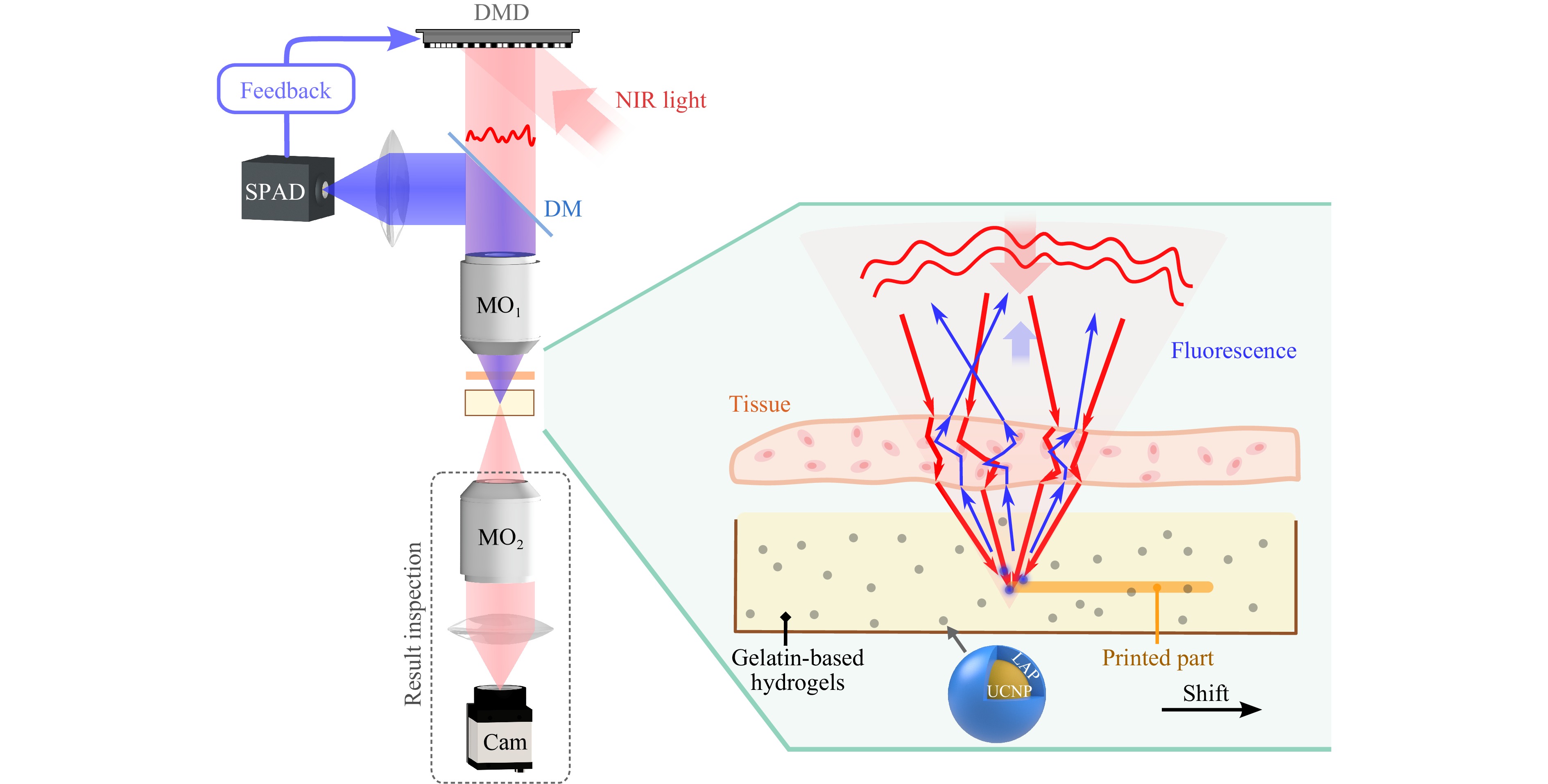
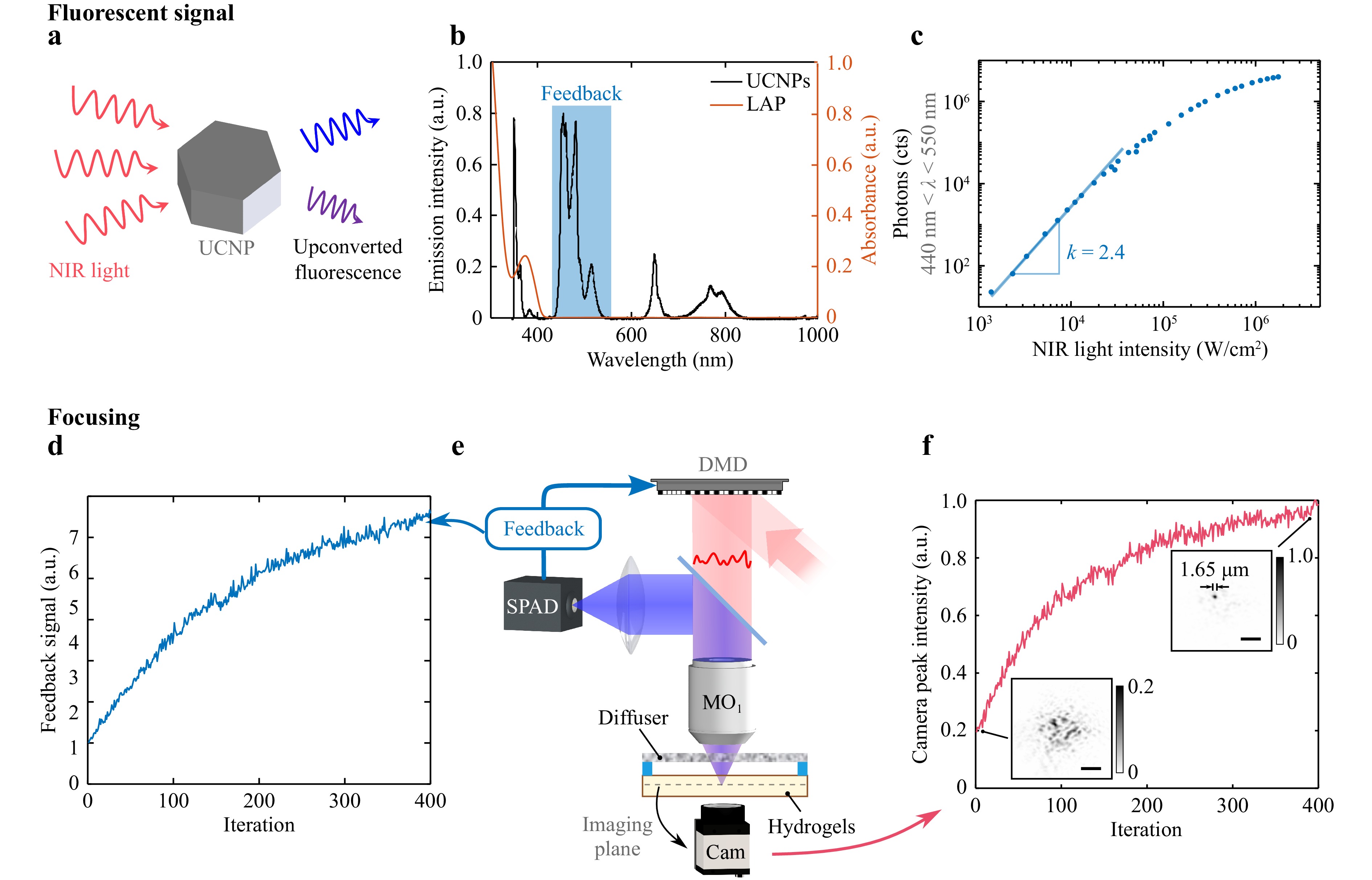
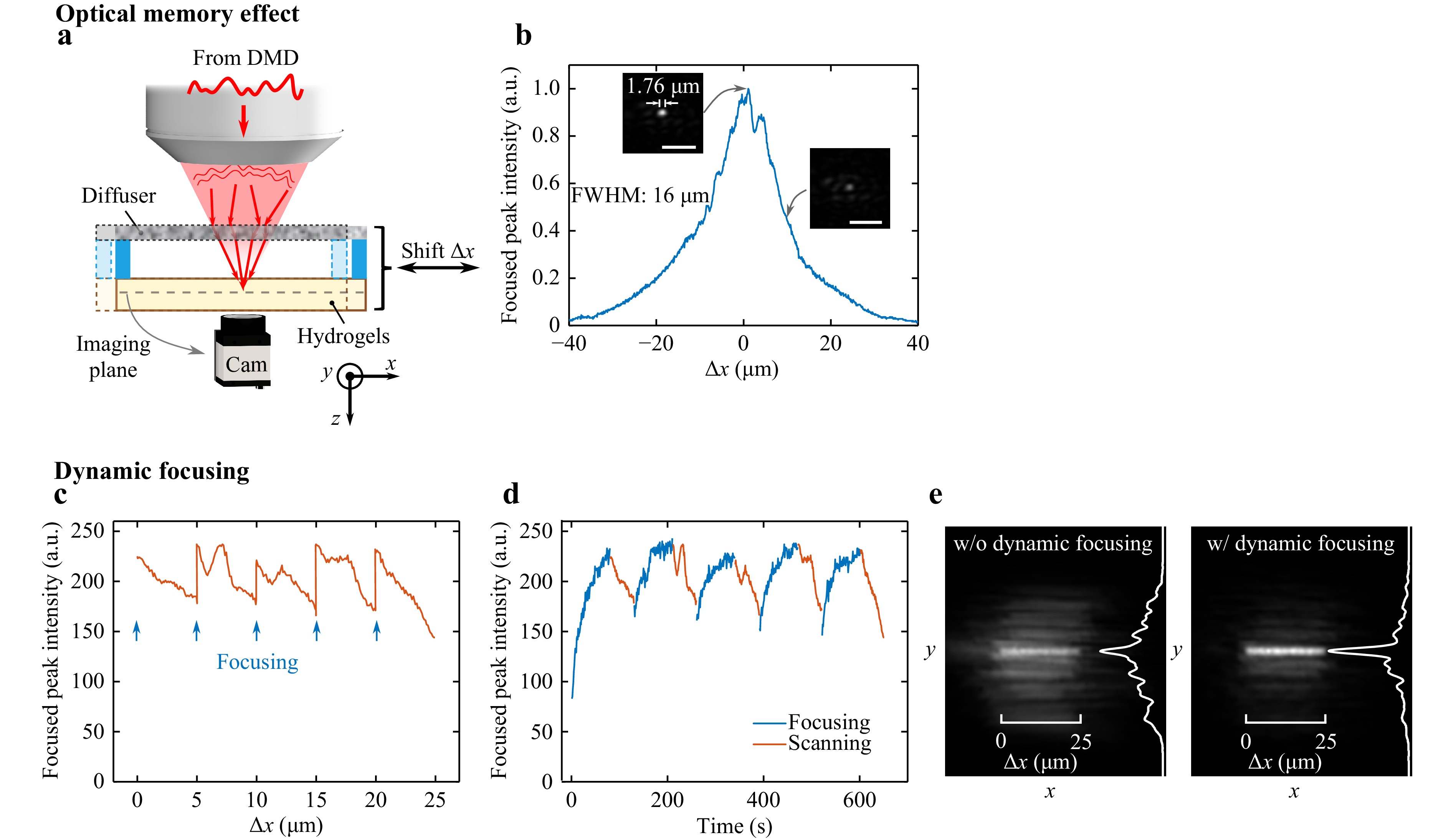
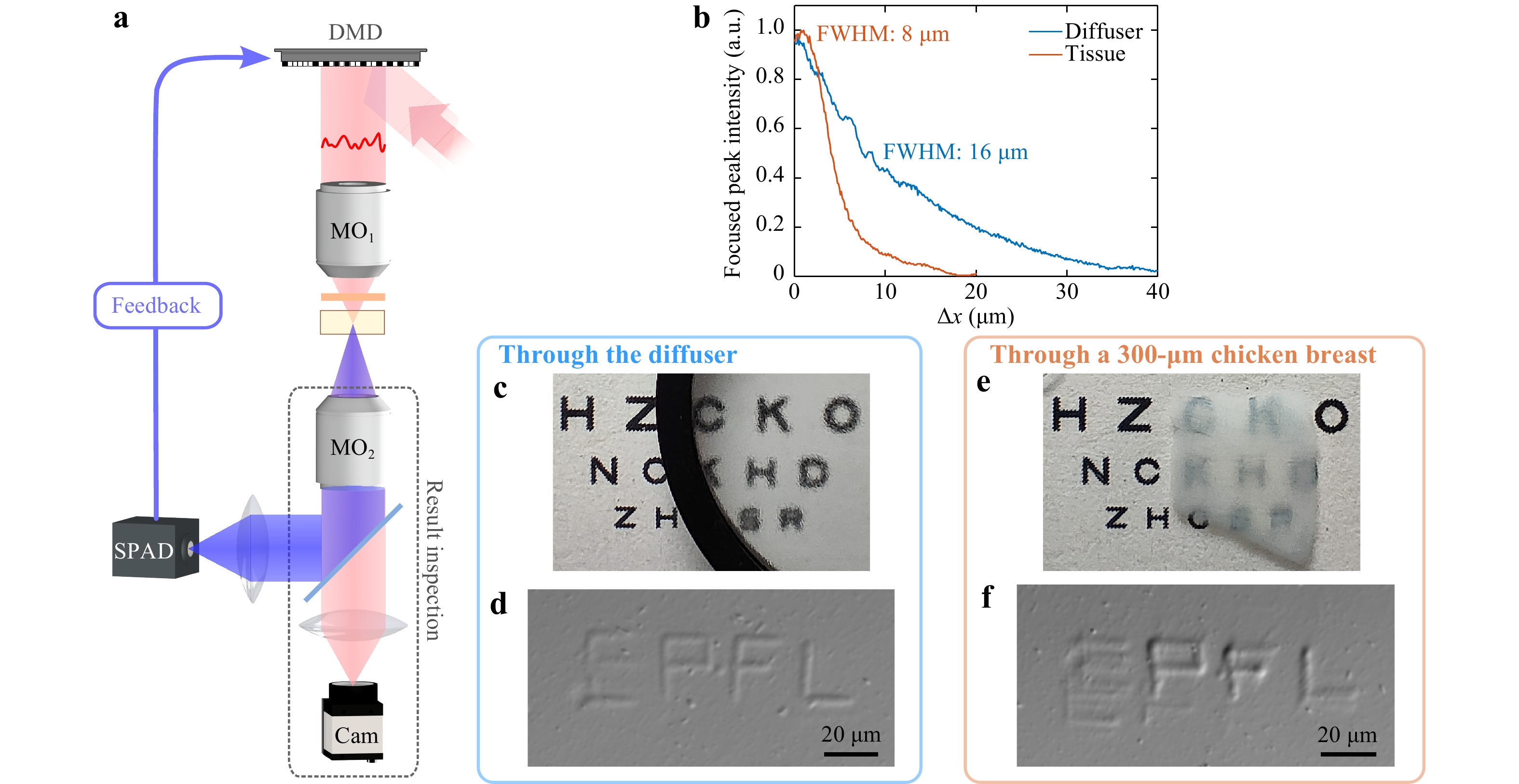
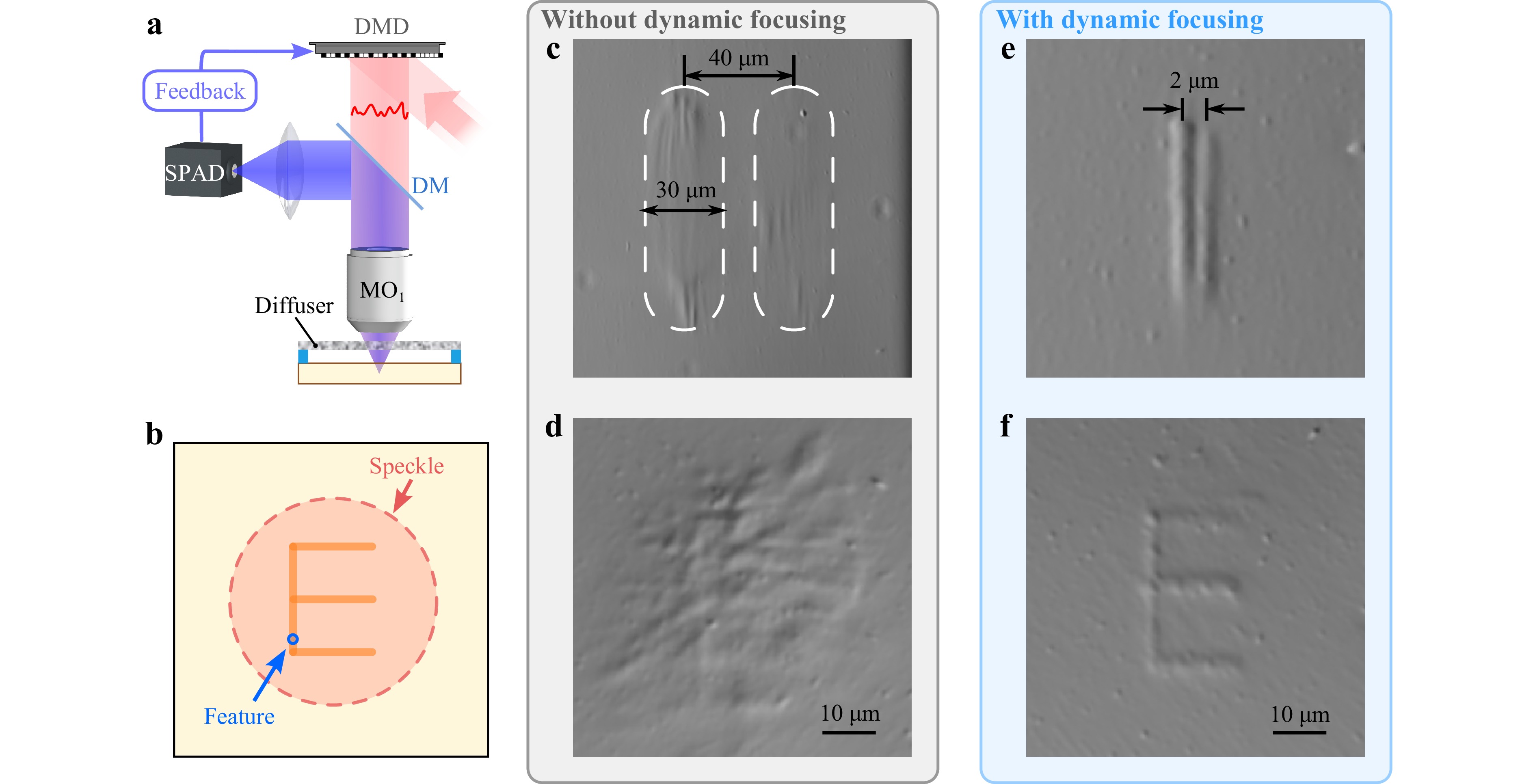
Light-based additive manufacturing holds great potential in the field of bioprinting due to its exceptional spatial resolution, enabling the reconstruction of intricate tissue structures. However, printing through biological tissues is severely limited due to the strong optical scattering within the tissues. The propagation of light is scrambled to form random speckle patterns, making it impossible to print features at the diffraction-limited size with conventional printing approaches. The poor tissue penetration depth of ultra-violet or blue light, which is commonly used to trigger photopolymerization, further limits the fabrication of high cell-density tissue constructs. Recently, several strategies based on wavefront shaping have been developed to manipulate the light and refocus it inside scattering media to a diffraction-limited spot. In this study, we present a high-resolution additive manufacturing technique using upconversion nanoparticles and a wavefront shaping method that does not require measurement from an invasive detector, i.e., it is a non-invasive technique. Upconversion nanoparticles convert near-infrared light to ultraviolet and visible light. The ultraviolet light serves as a light source for photopolymerization and the visible light as a guide star for digital light shaping. The incident light pattern is manipulated using the feedback information of the guide star to focus light through the tissue. In this way, we experimentally demonstrate that near-infrared light can be non-invasively focused through a strongly scattering medium. By exploiting the optical memory effect, we further demonstrate micro-meter resolution additive manufacturing through highly scattering media such as a 300-μm-thick chicken breast. This study provides a concept of high-resolution additive manufacturing through turbid media with potential application in tissue engineering.
Published. 2025, 6(2)
: 260-271
doi: 10.37188/lam.2025.029
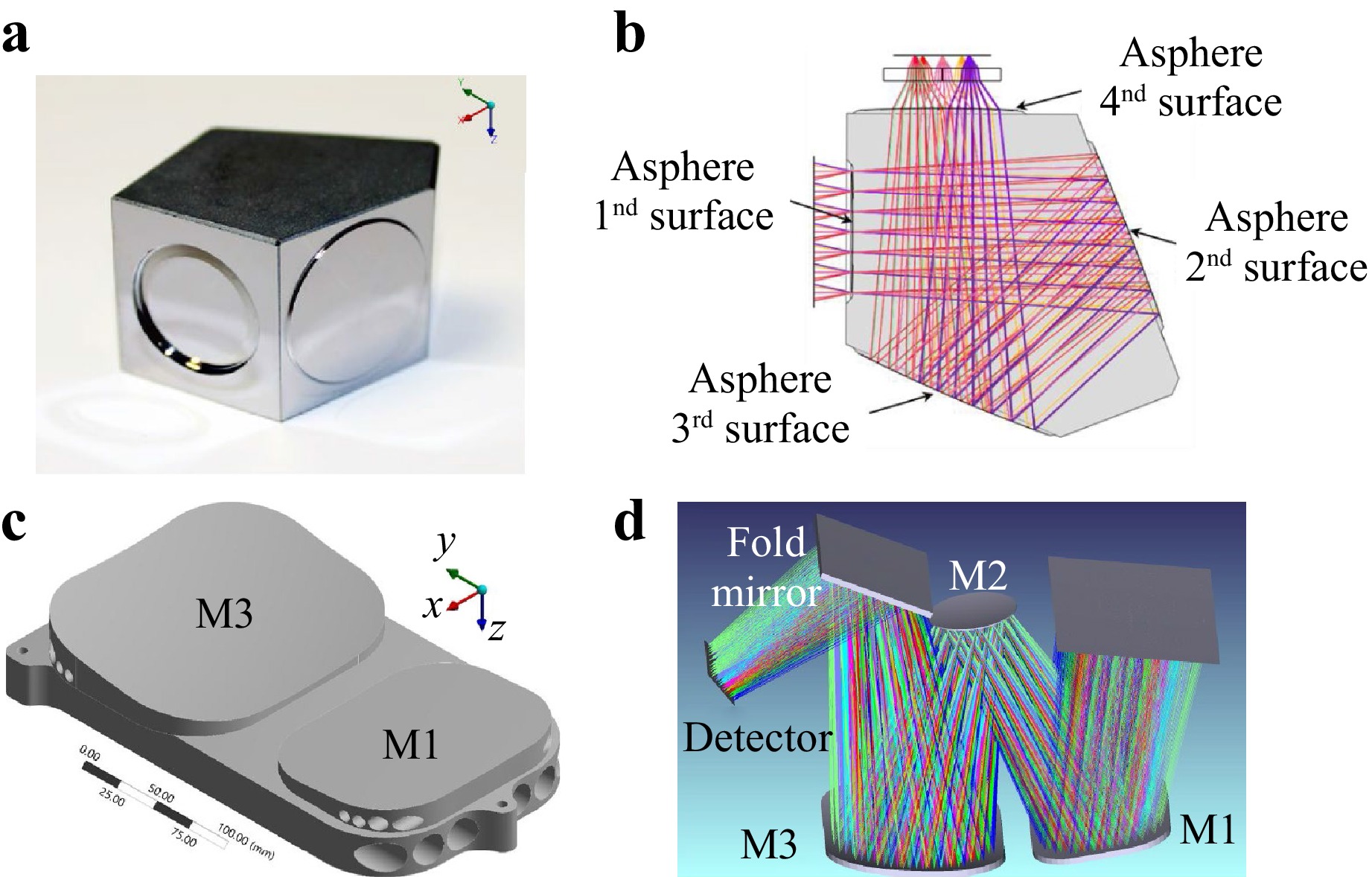
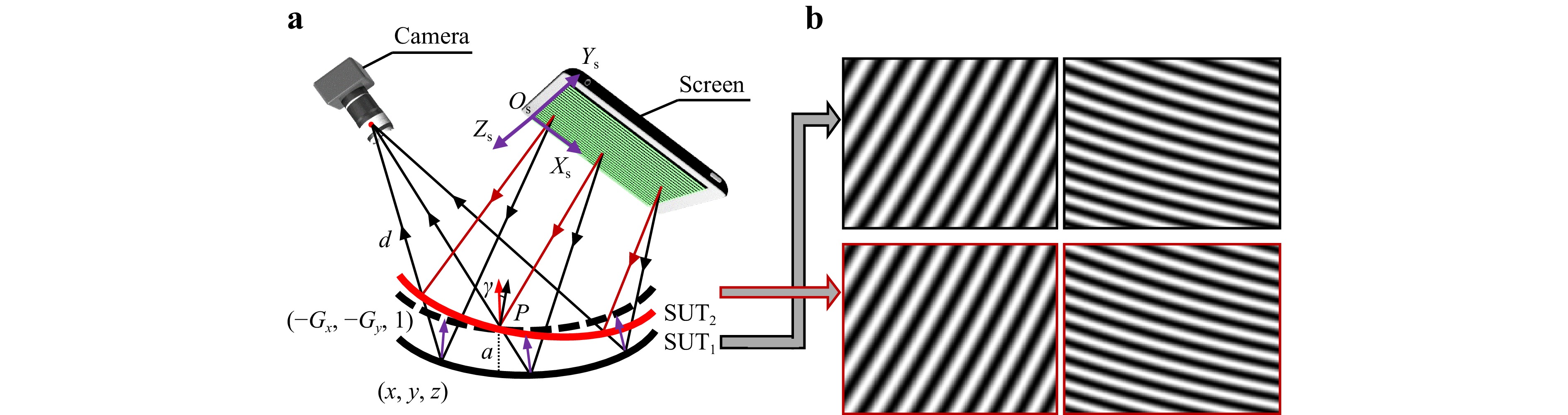
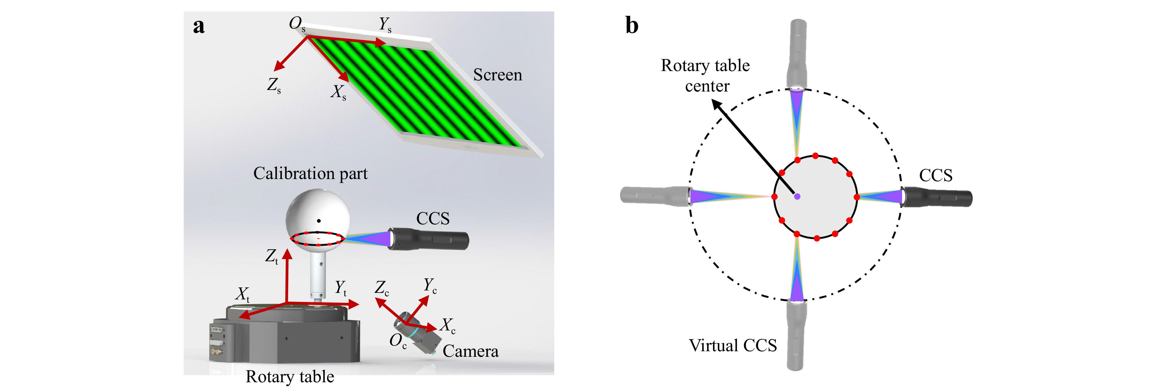
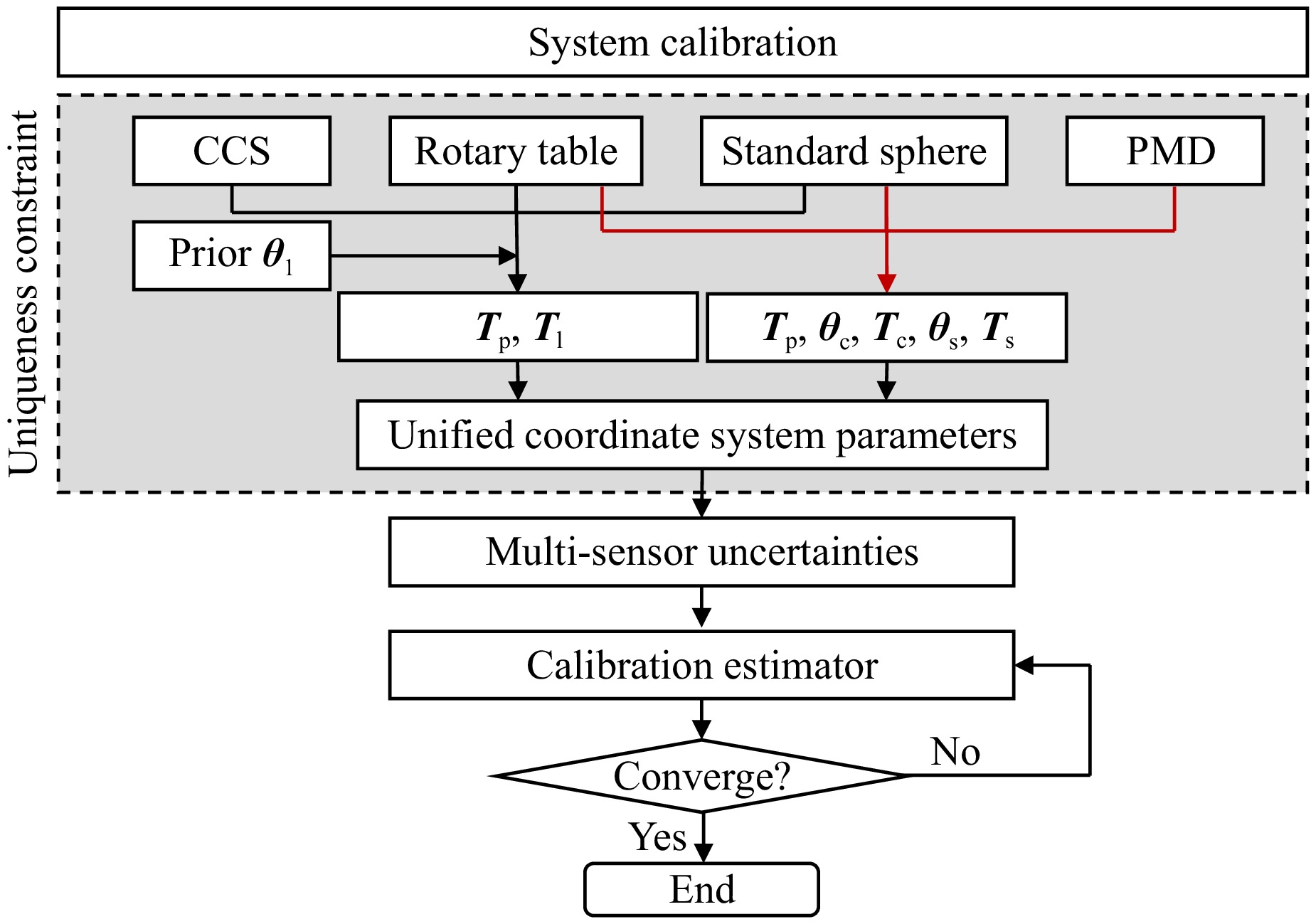
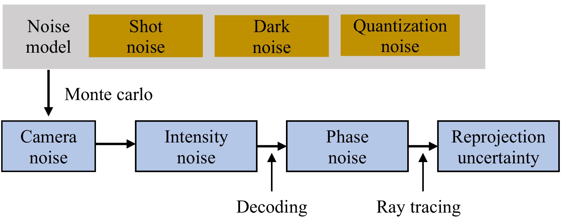
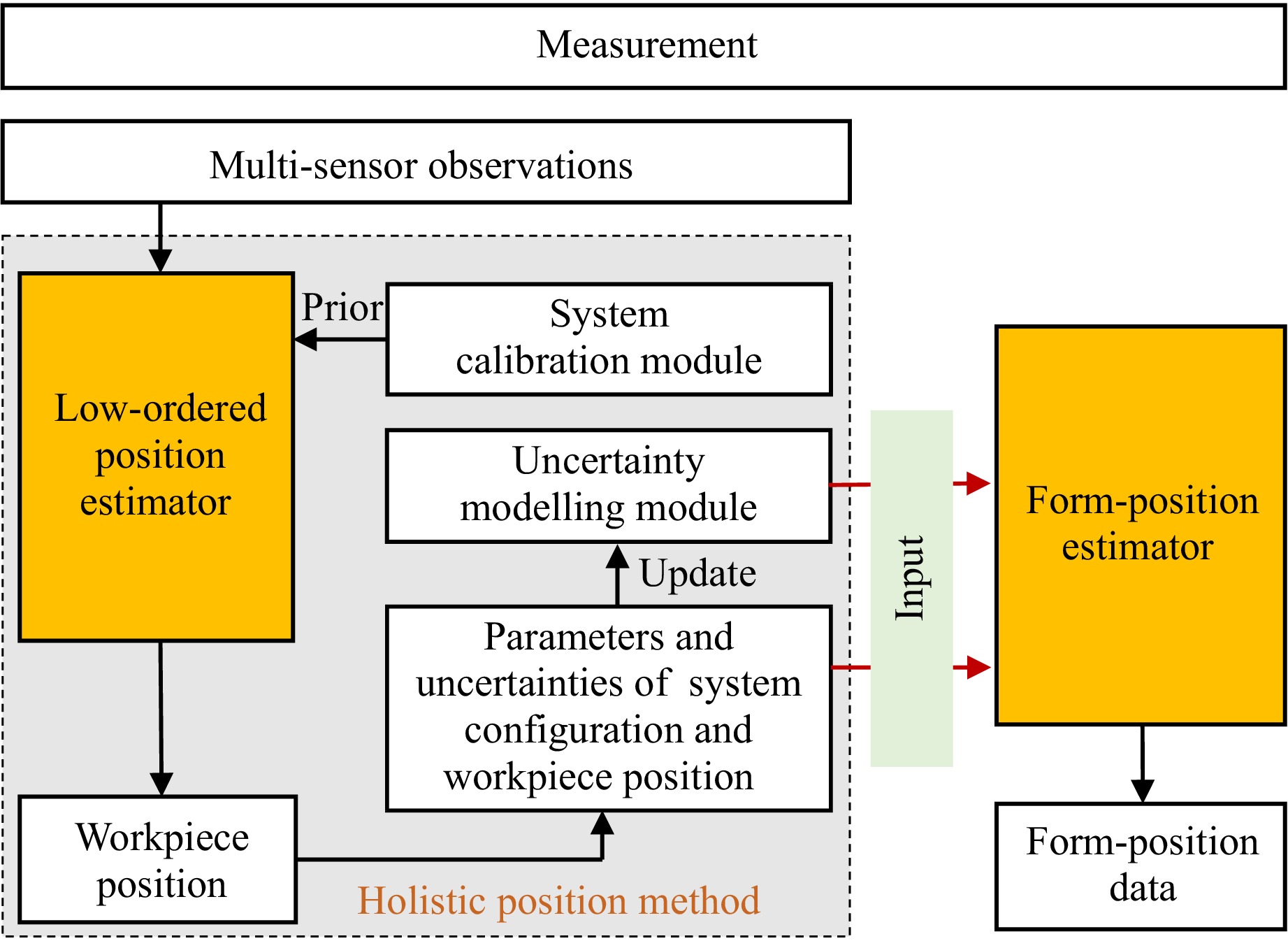
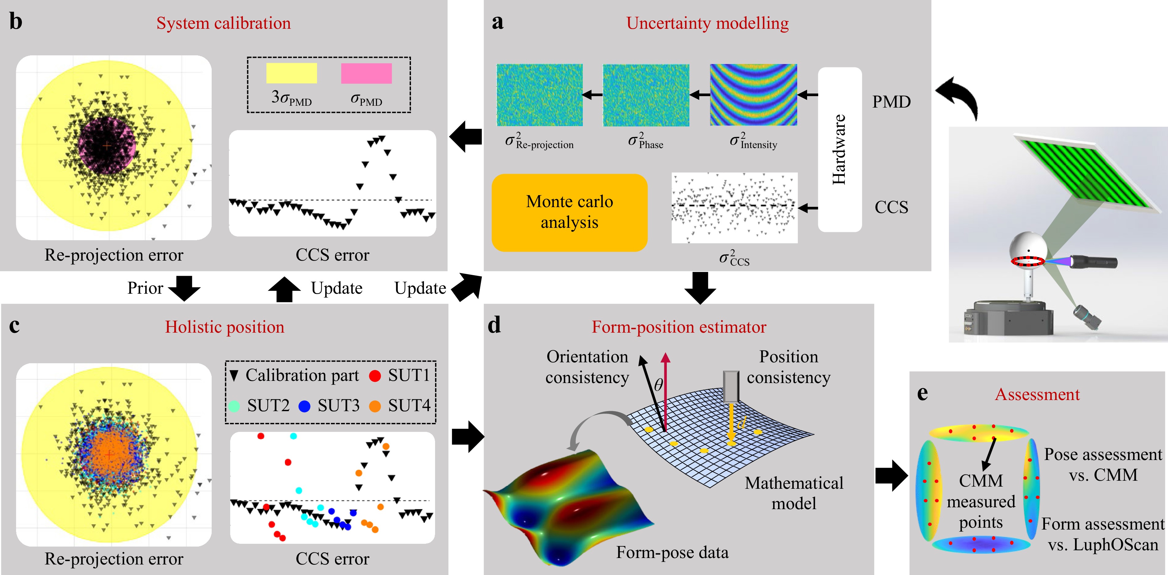
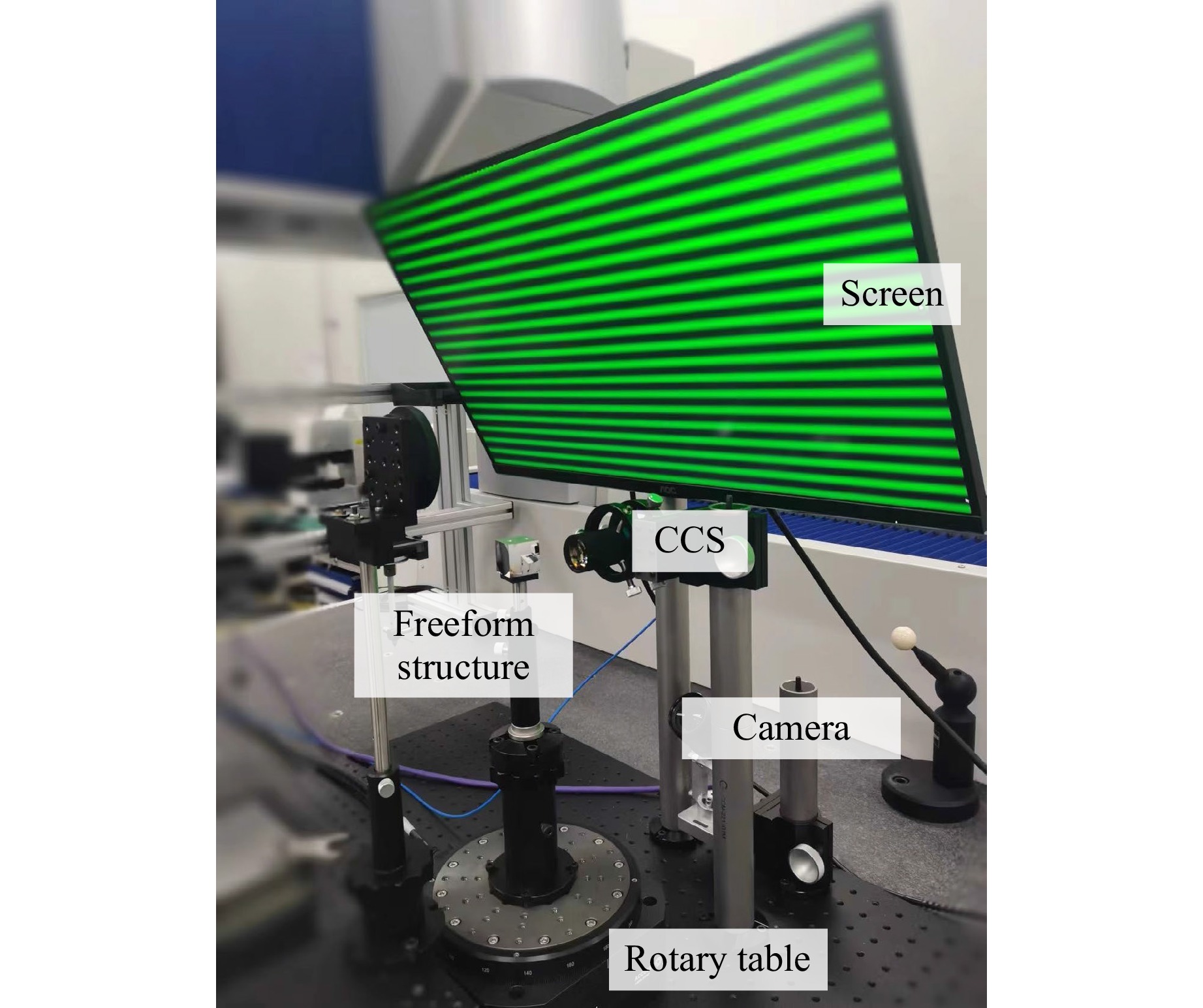
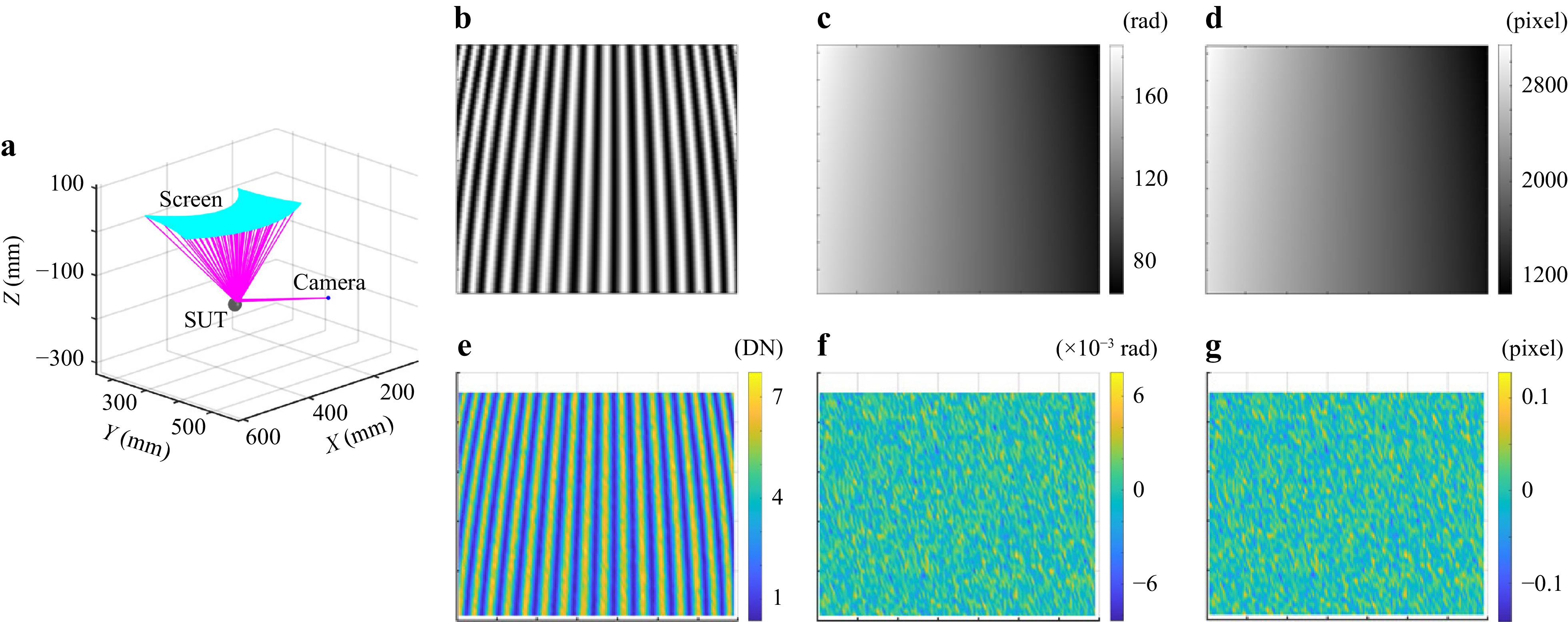
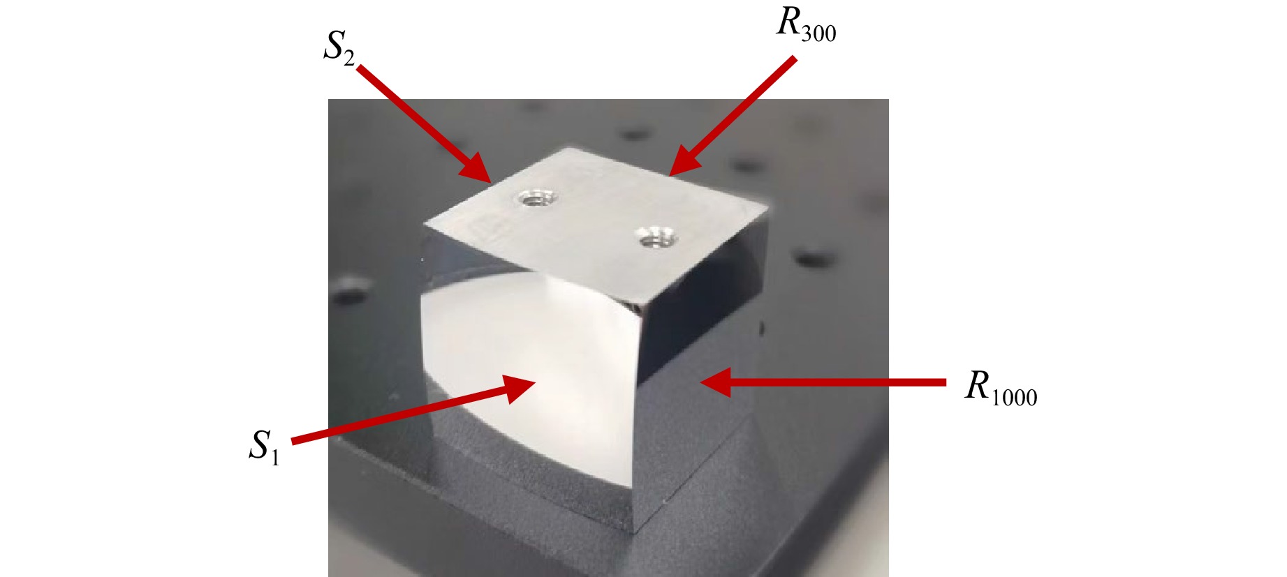
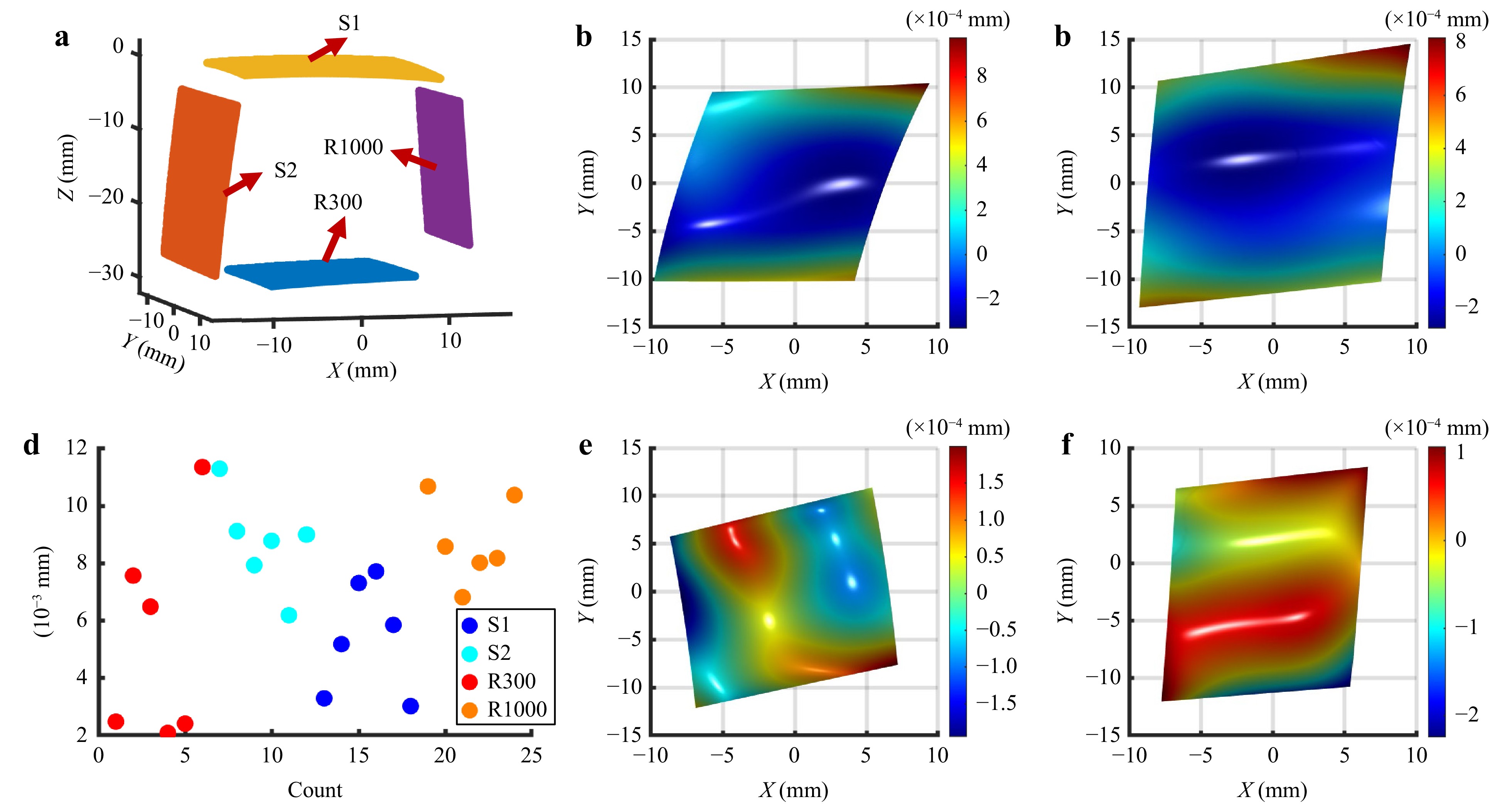
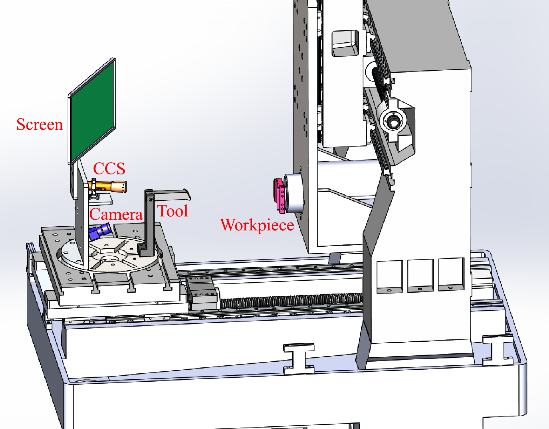
Monolithic multi-freeform optical structures play significant roles in advanced optical systems by simplifying system structures and enhancing optoelectronic performance. However, manufacturing and measurement present significant challenges, which require the simultaneous assurance of form quality and relative positioning of multiple functional surfaces. Consequently, a deterministic form-position deflectometric measuring method is proposed based on Bayesian multisensor fusion, which effectively overcomes the inherent limitation of deflectometry in absolute positioning. Calibration priors were marginalised in the measurement model to improve fidelity, and a fully probabilistic measurement framework was proposed to eliminate numerical bias in conventional sequential optimisation approaches. Finally, a geometric-constraint-based registration method was developed to evaluate the form-position quality of freeform surfaces. The experimental results demonstrated the measurement accuracy could achieve a level of one hundred nanometres for surface forms and a few microns for surface positions.
Published. 2025, 6(2)
: 272-283
doi: 10.37188/lam.2025.031
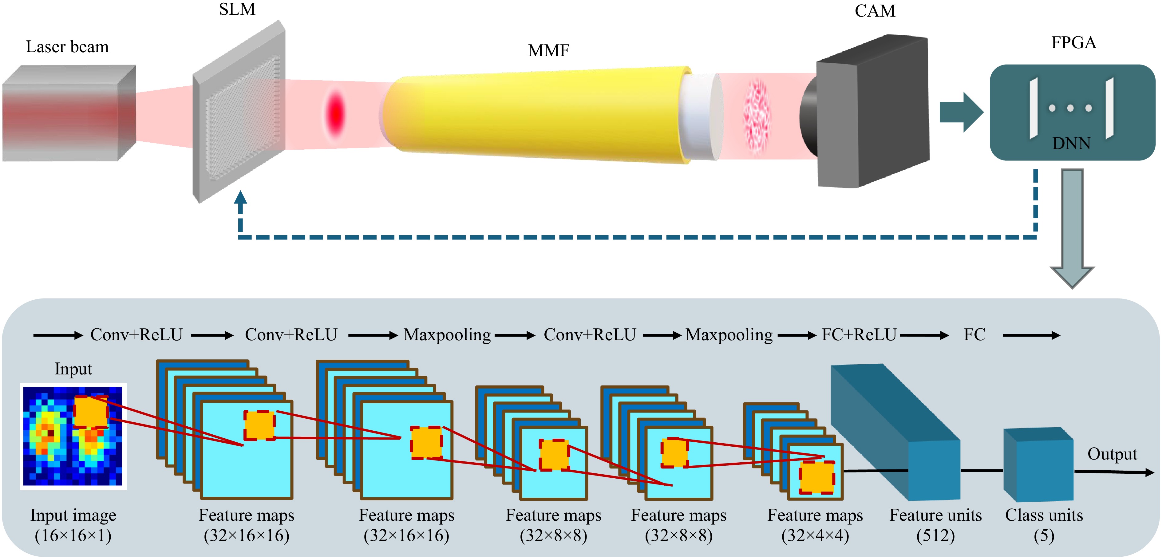
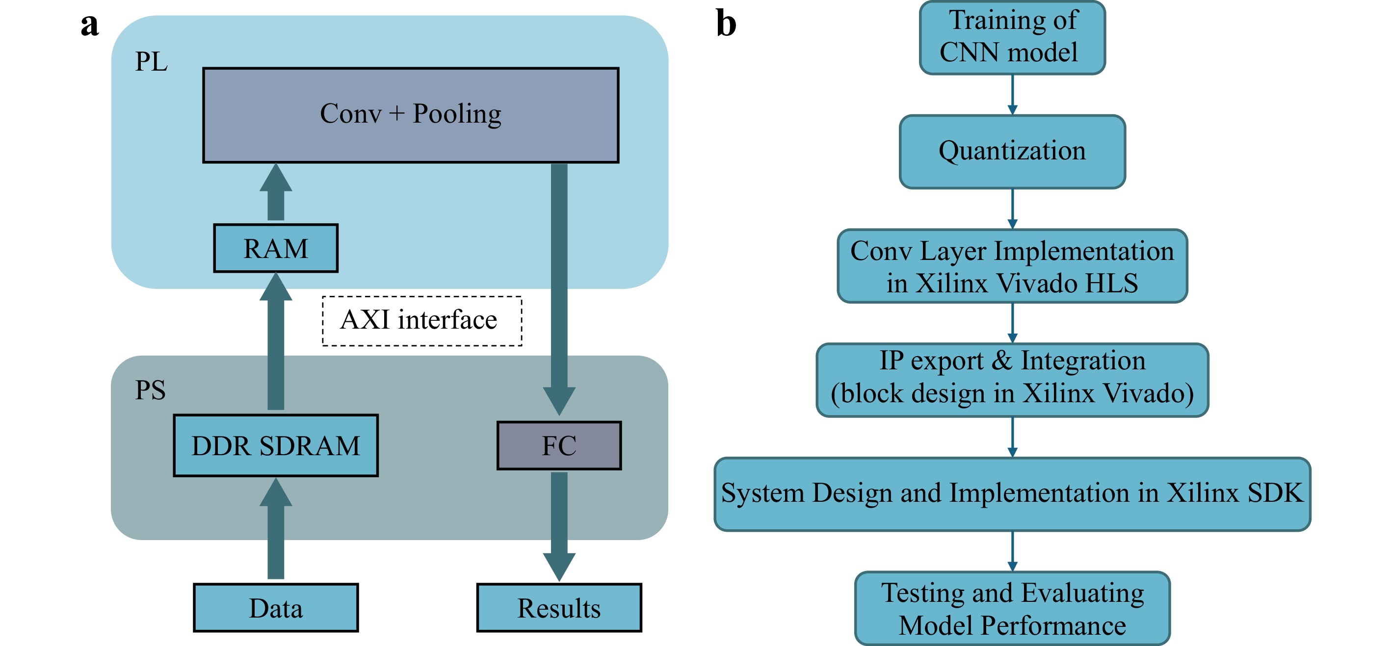
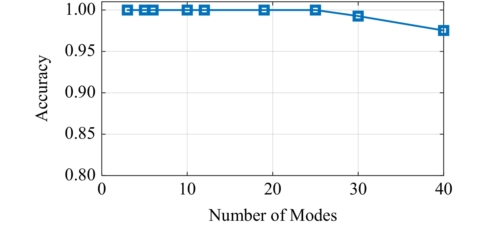
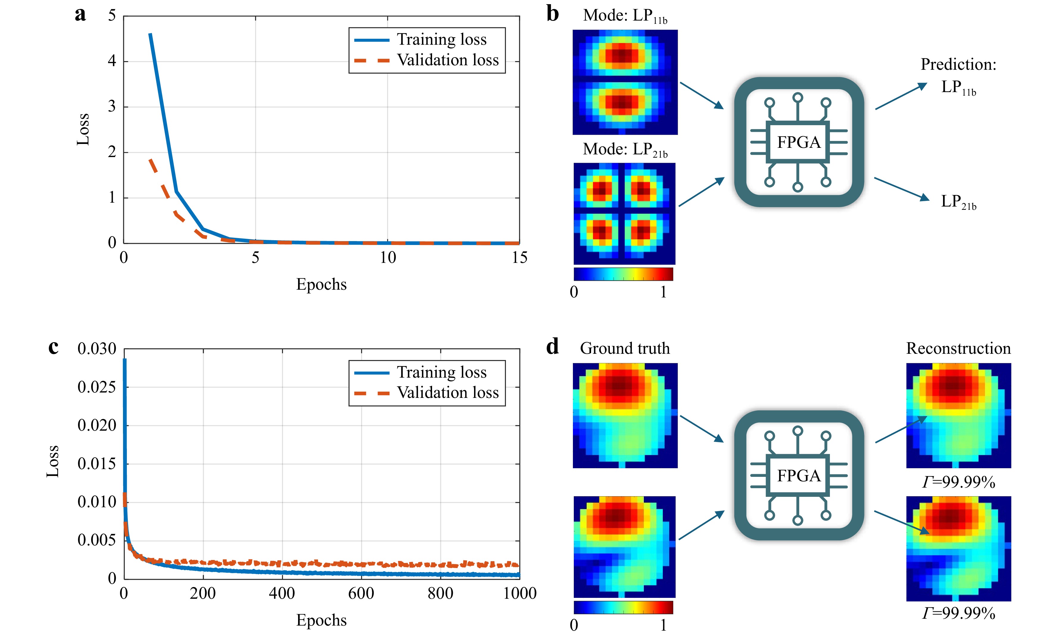
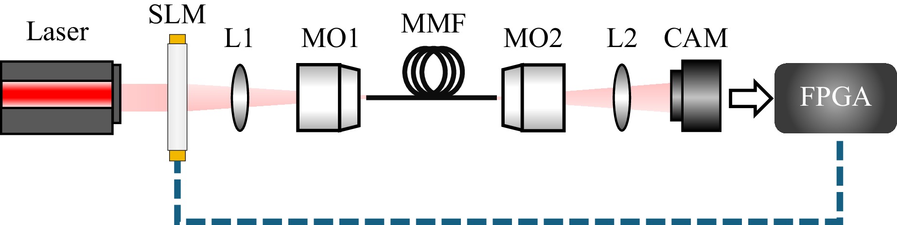
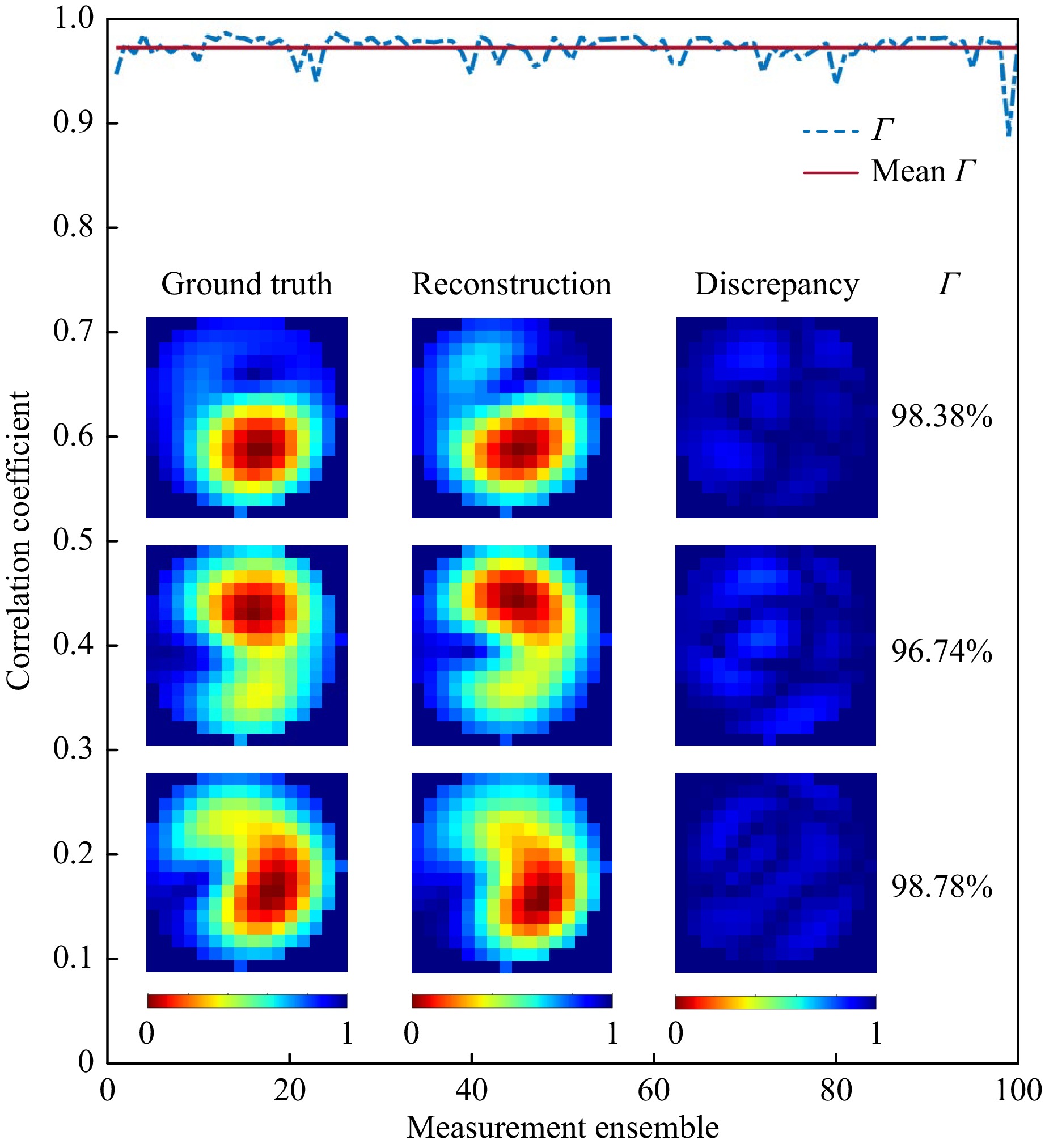
Mode division multiplexing (MDM) using multimode fibers (MMFs) is key to meeting the demand for higher data rates and advancing internet technologies. However, optical transmission within MMFs presents challenges, particularly due to mode crosstalk, which complicates the use of MMFs to increase system capacity. Quantitatively analyzing the output of MMFs is essential not only for telecommunications but also for applications like fiber sensors, fiber lasers, and endoscopy. With the success of deep neural networks (DNNs), AI-driven mode decomposition (MD) has emerged as a leading solution for MMFs. However, almost all implementations rely on Graphics Processing Units (GPUs), which have high computational and system integration demands. Additionally, achieving the critical latency for real-time data transfer in closed-loop systems remains a challenge. In this work, we propose using field-programmable gate arrays (FPGAs) to perform neural network inference for MD, marking the first use of FPGAs for this application, which is important, since the latency of closed-loop control could be significantly lower than at GPUs. A convolutional neural network (CNN) is trained on synthetic data to predict mode weights (amplitude and phase) from intensity images. After quantizing the model’s parameters, the CNN is executed on an FPGA using fixed-point arithmetic. The results demonstrate that the FPGA-based neural network can accurately decompose up to six modes. The FPGA’s customization and high efficiency provide substantial advantages, with low power consumption (2.4 Watts) and rapid inference (over 100 Hz), offering practical solutions for real-time applications. The proposed FPGA-based MD solution, coupled with closed-loop control, shows promise for applications in fiber characterization, communications, and beyond.
Published. 2025, 6(2)
: 284-294
doi: 10.37188/lam.2025.035
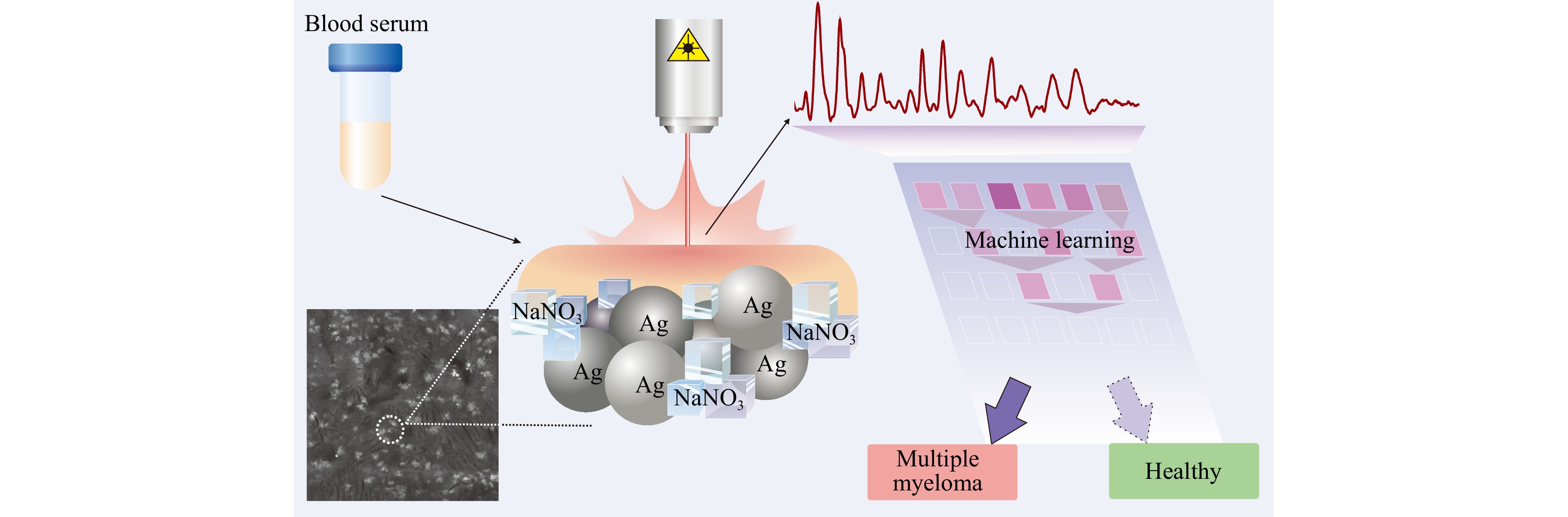
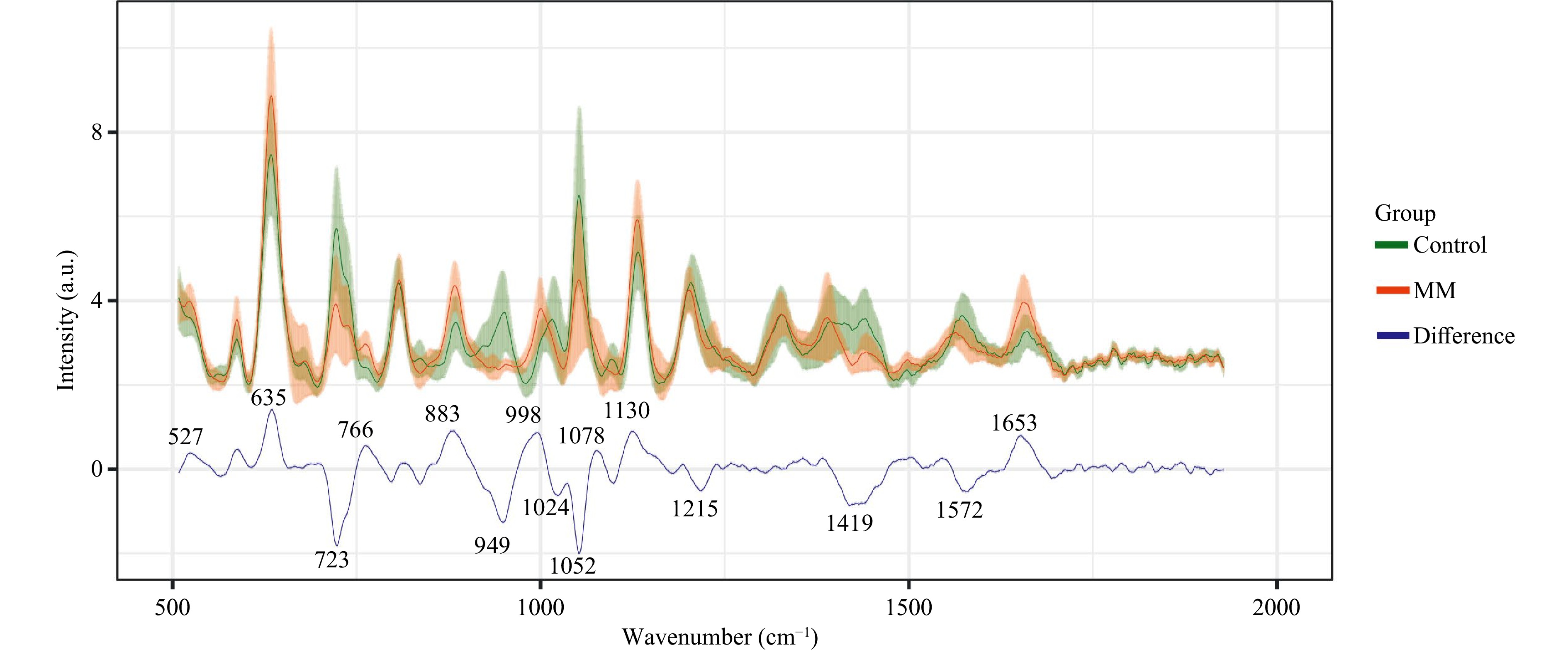
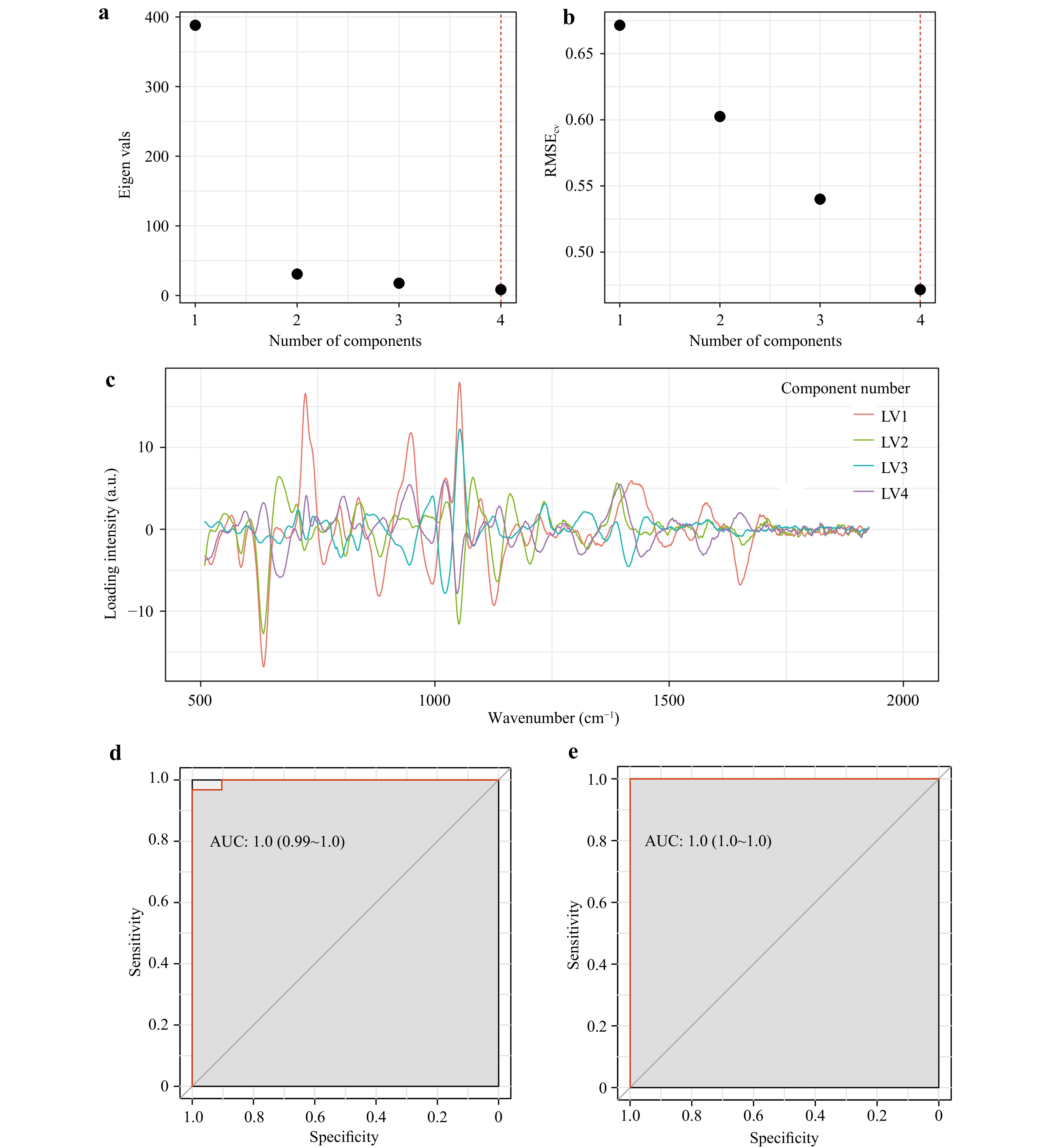
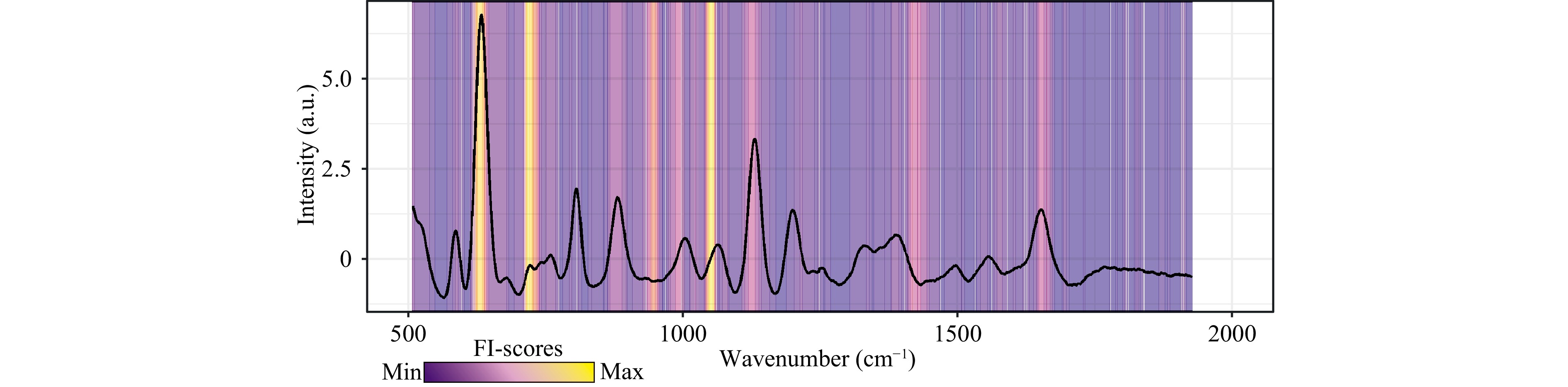
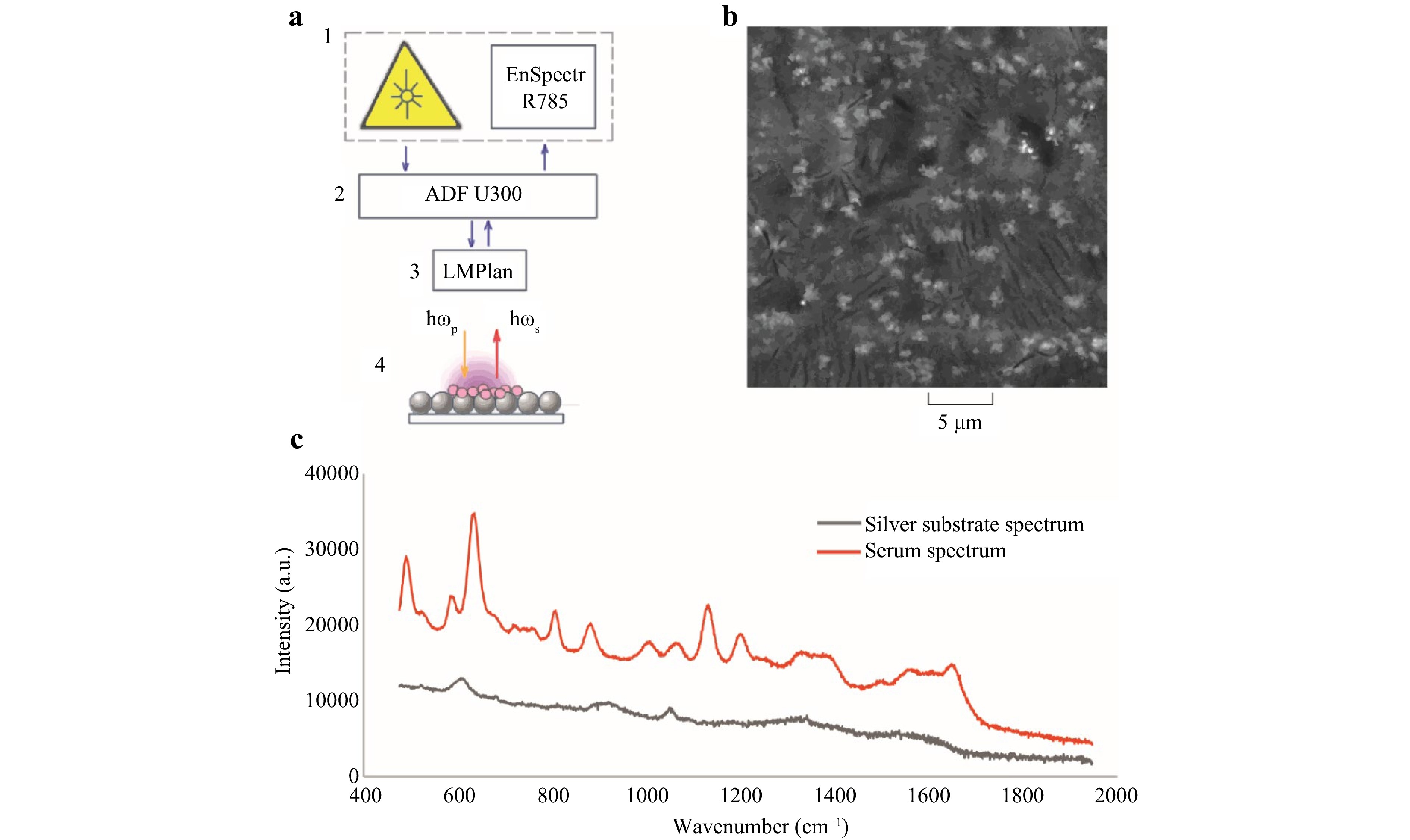
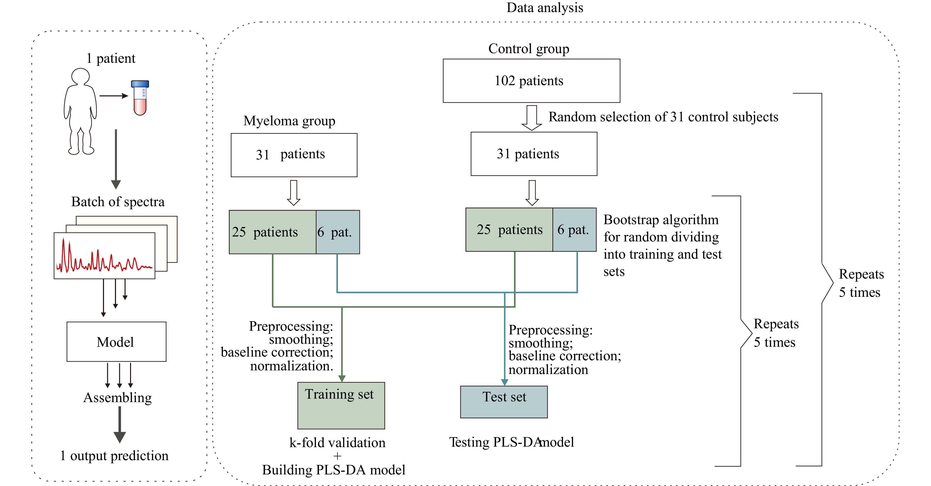
Surface-enhanced Raman spectroscopy (SERS) is a promising analytical method for studying the structure and composition of multi-component media in clinical practice. However, the practical application of SERS imposes several conditions and restrictions depending on the required analytical accuracy and implementation complexity. This paper proposes a simple serum SERS technique for diagnosing multiple myeloma (MM). The process utilises a substrate composed of agglomerated spherical silver particles (~200 nm) with a capillary effect on sodium nitrate crystals (0.02% volume concentration), excited at a wavelength of 785 nm. Spectral characteristics were recorded using a detector without external cooling, ensuring a cost-effective approach. The proposed low-cost approach was tested on 31 samples from MM and 102 serum samples from an age-matched control group. Combining the SERS technique with the multivariate analysis for serum testing provided high discrimination rates for MM patients compared to the control patients, with an average accuracy of over 96%. Biochemical interpretation of the recorded spectra identified the informative bands at 635 cm-1, 723 cm-1, and 1052 cm-1. Overall, the proposed SERS-based tool can become the basis for screening for MM and can be easily integrated into clinical practice, expanding diagnostic capabilities where expensive laboratory techniques are not affordable.
Dual-modal spatiotemporal imaging of ultrafast dynamics in laser-induced periodic surface structures
Published. 2025, 6(2)
: 295-305
doi: 10.37188/lam.2025.030
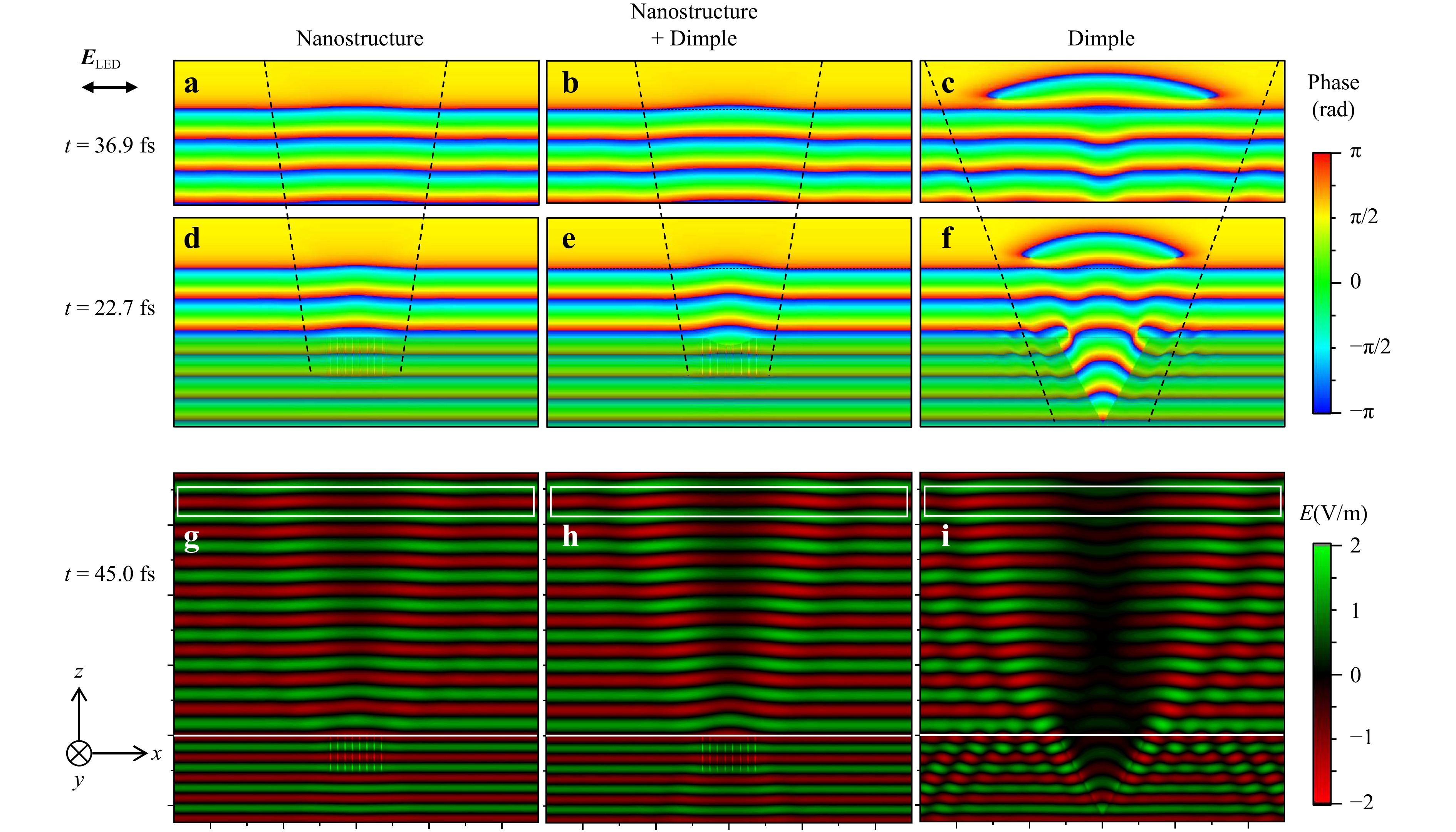
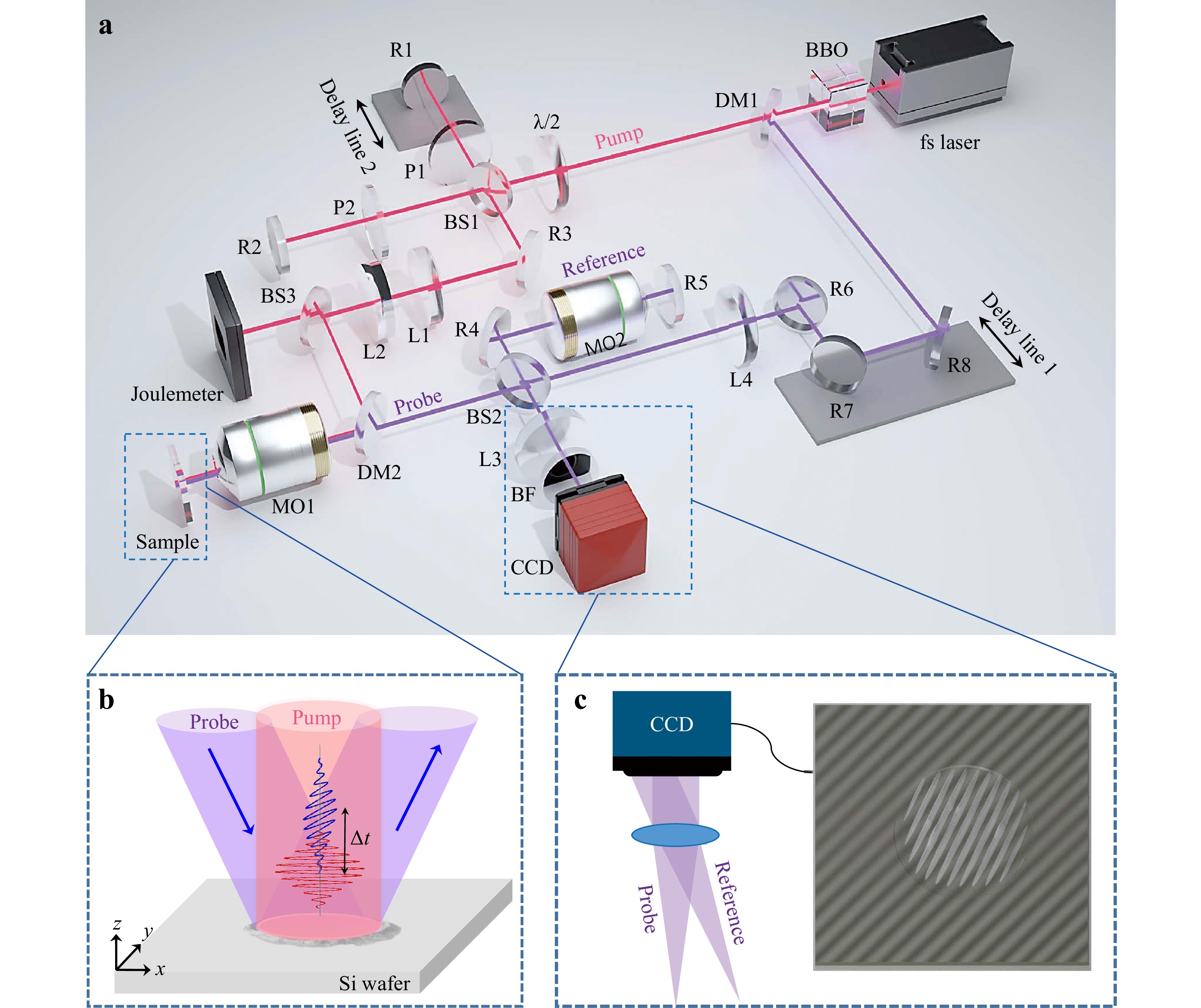
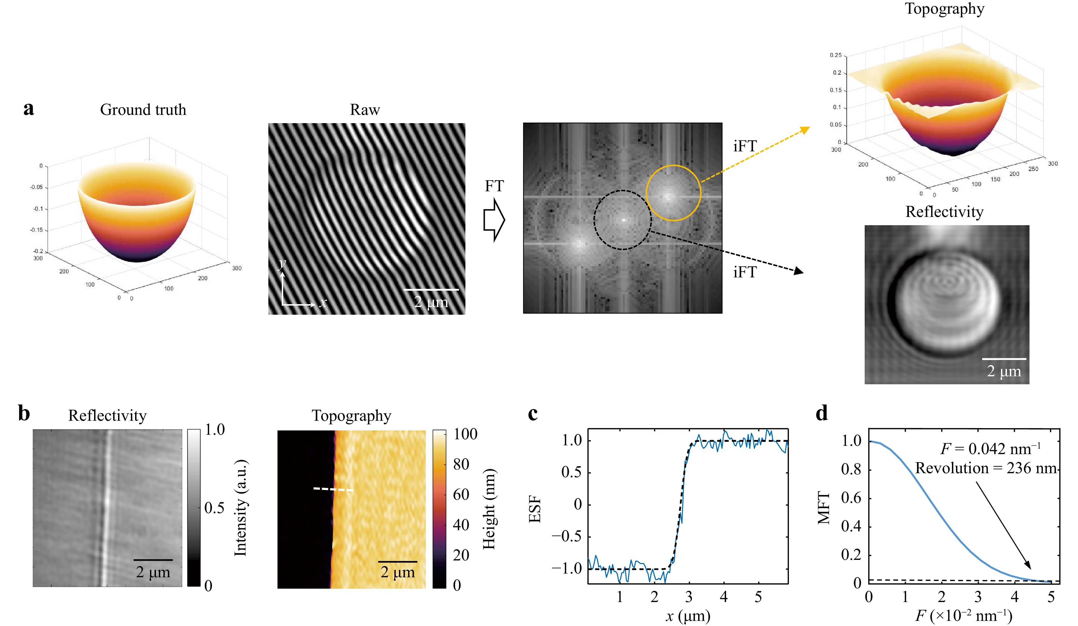
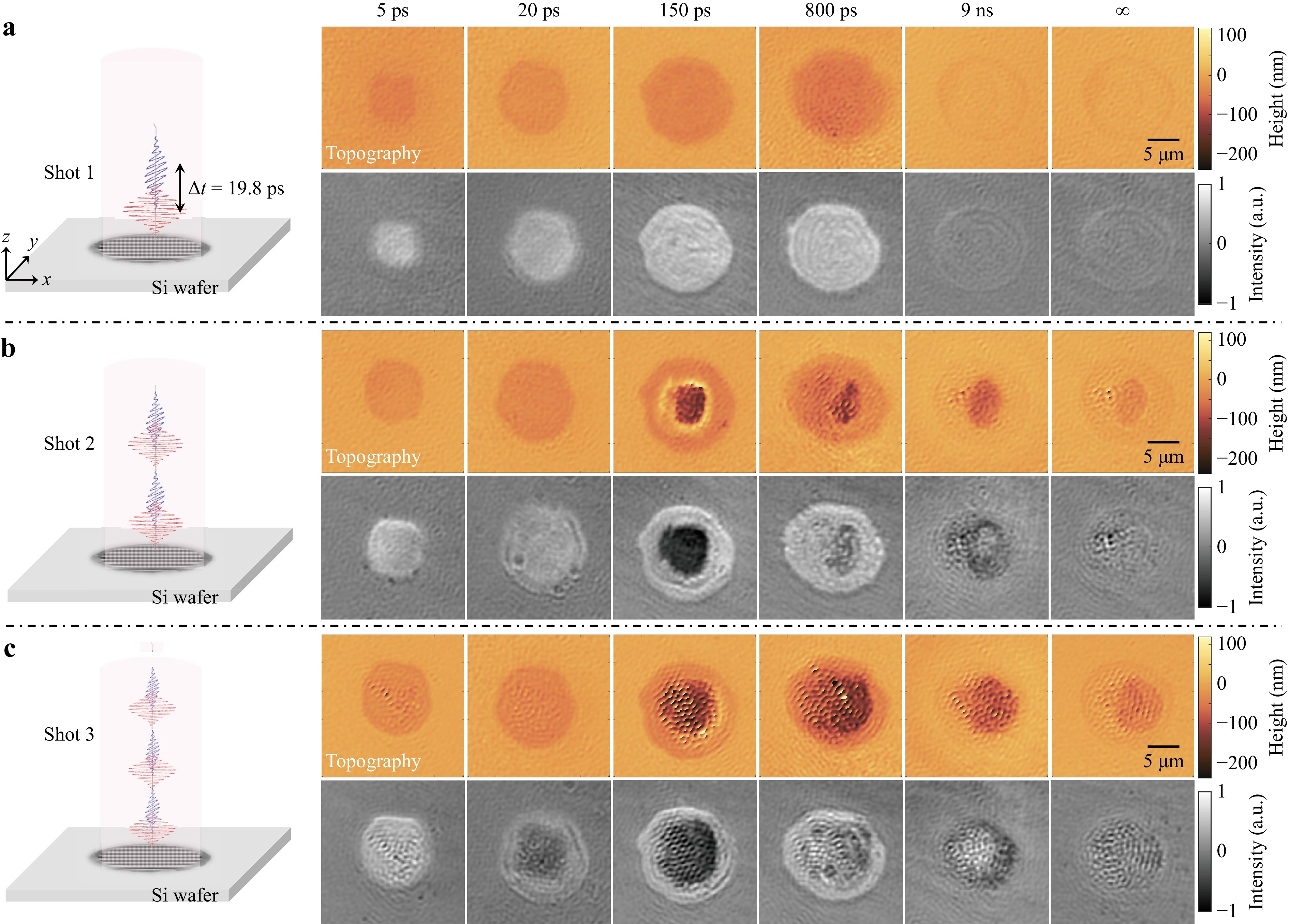
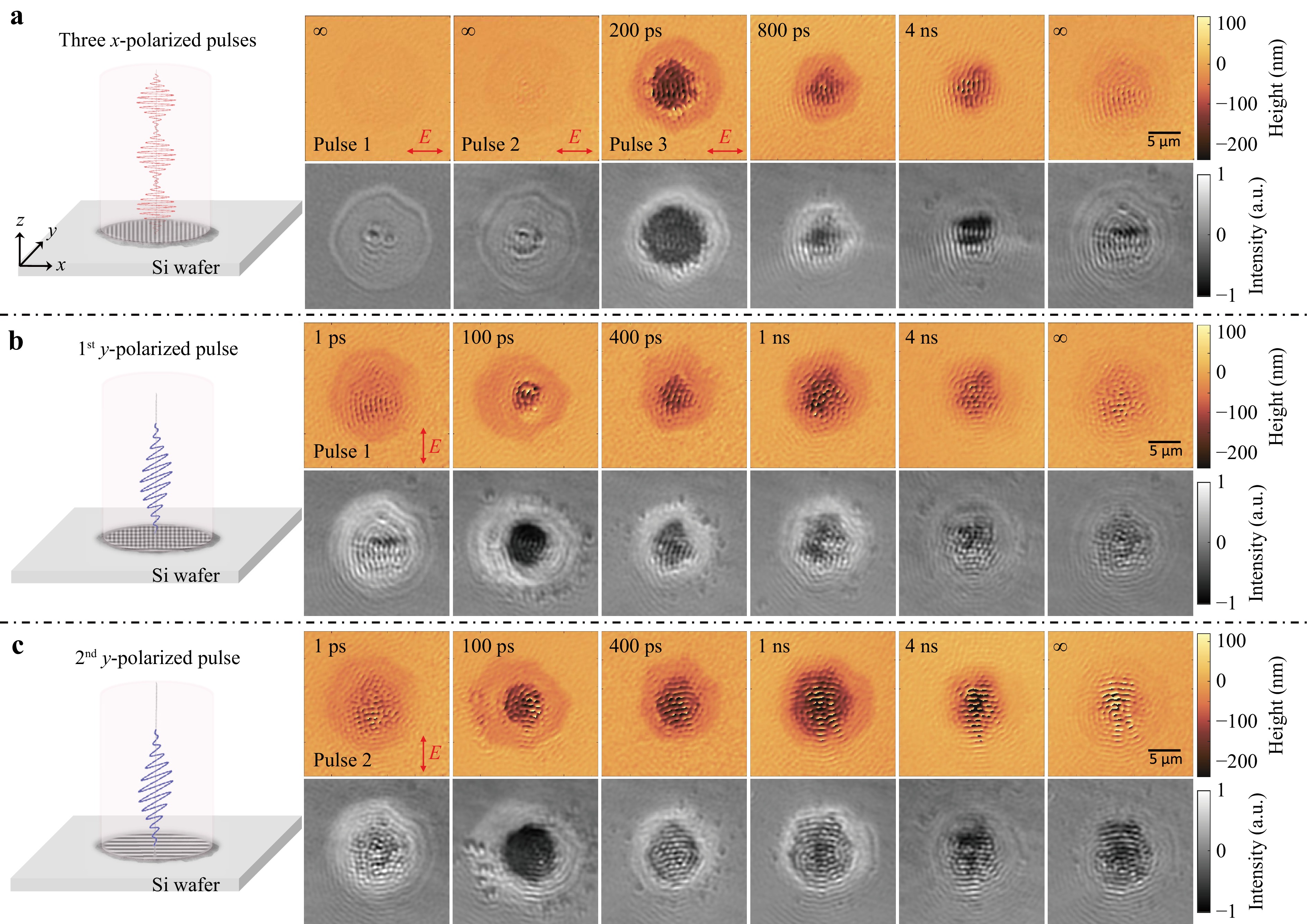
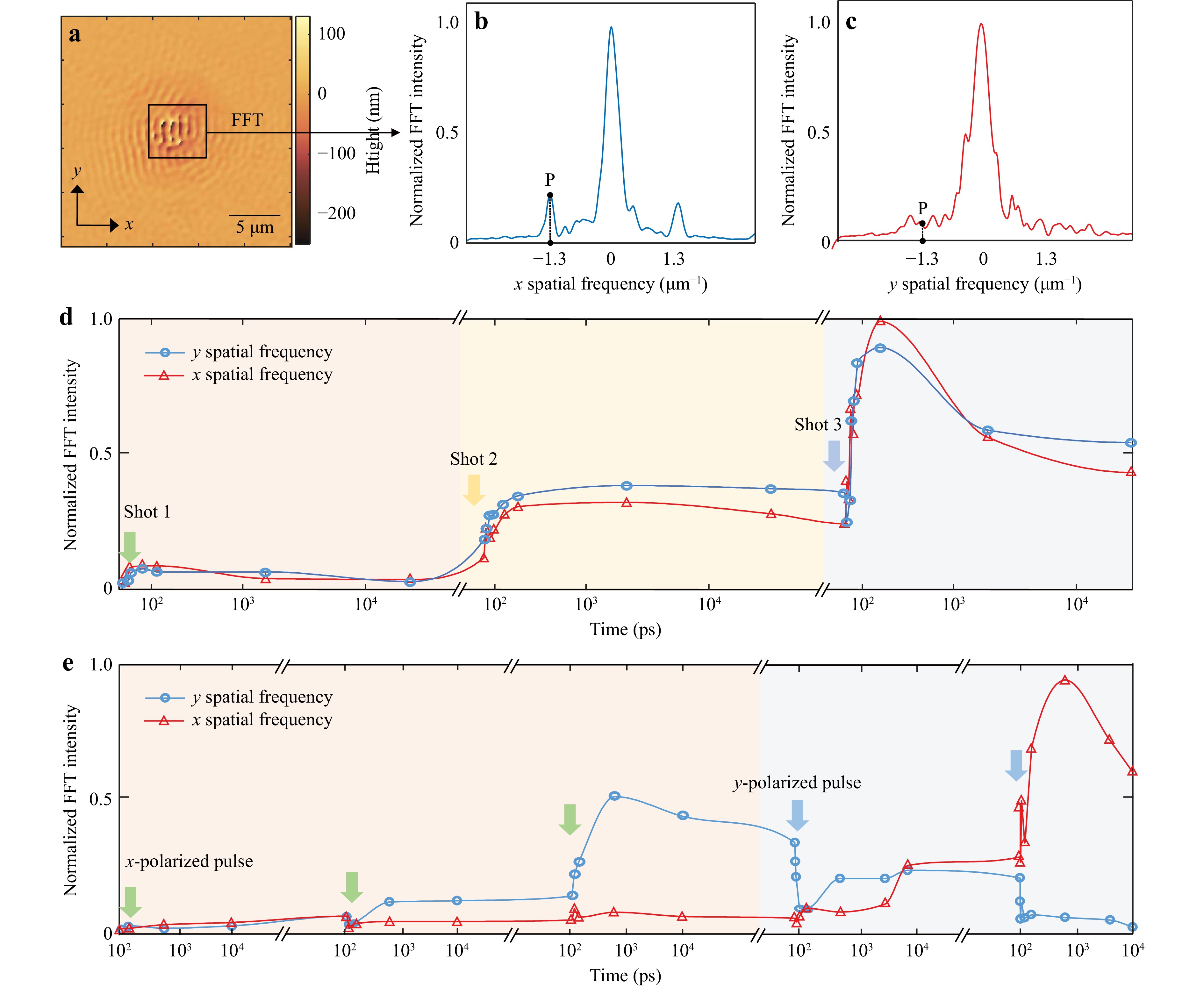
The interactions between ultrafast lasers and materials reveal a range of nonlinear transient phenomena that are crucial in advanced manufacturing. Understanding these interactions during ultrafast laser ablation requires detailed measurements of material properties and structural changes with high temporal and spatial resolutions. Traditional spatiotemporal imaging techniques relying on reflective imaging often fail to capture comprehensive information, resulting in predominantly qualitative theoretical models of these interactions. To overcome this limitation, we propose a dual-modal ultrafast microscopy system that combines two-dimensional reflectivity and three-dimensional topography imaging. By integrating pump-probe techniques with an interferometric imaging system, impressive spatiotemporal resolutions of 236 nm and 256 fs were achieved. Furthermore, using this system, we successfully examined the dynamics of laser-induced periodic surface structure formation, strengthening, and erasure on Si surfaces. The results demonstrate that the dual-modal spatiotemporal imaging technique can serve as a robust tool for the comprehensive analysis of ablation dynamics, facilitating a deeper understanding of the fundamental physics involved and enabling more accurate optimisation of ultrafast laser fabrication processes.
Published. 2025, 6(2)
: 306-318
doi: 10.37188/lam.2025.032
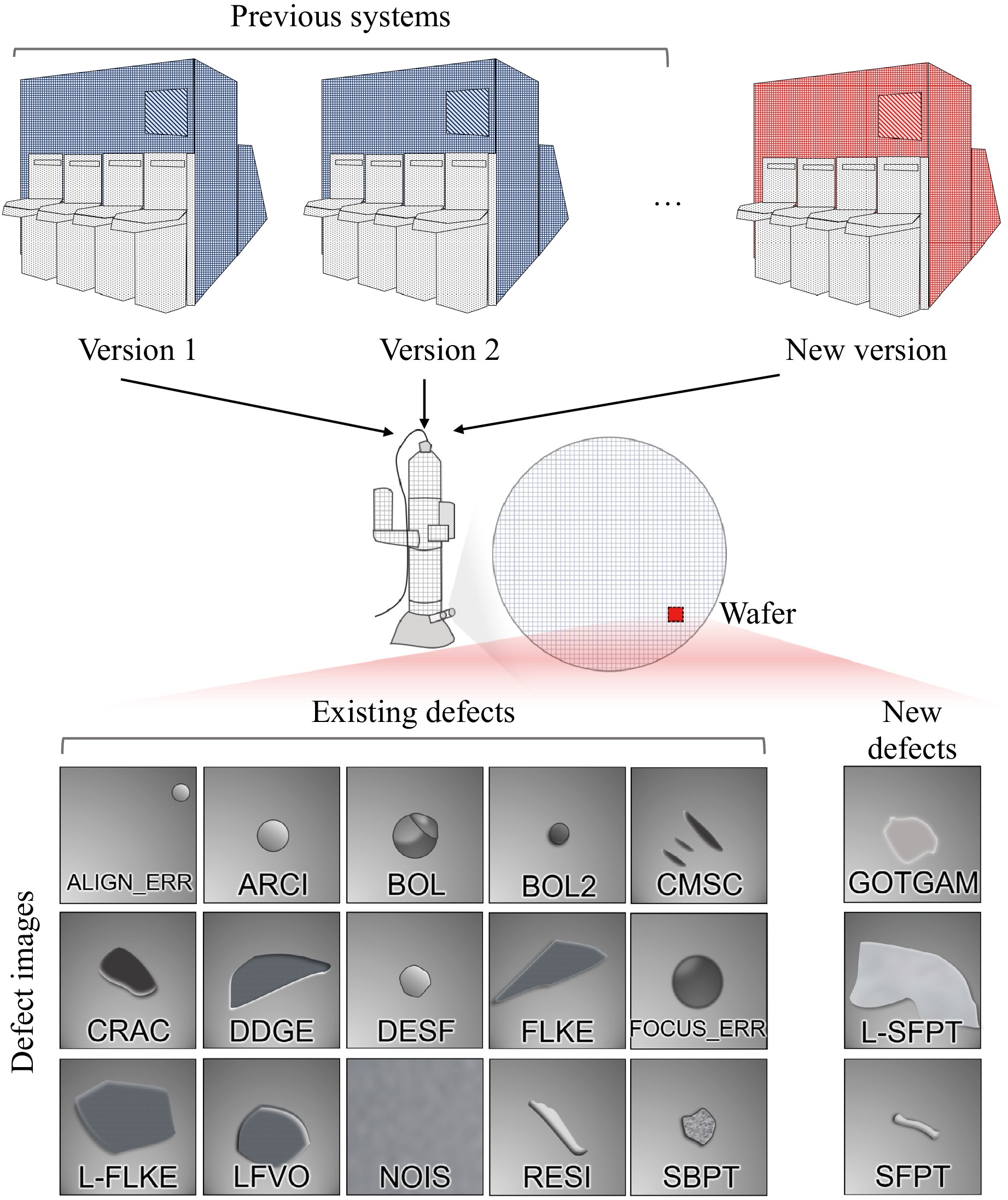
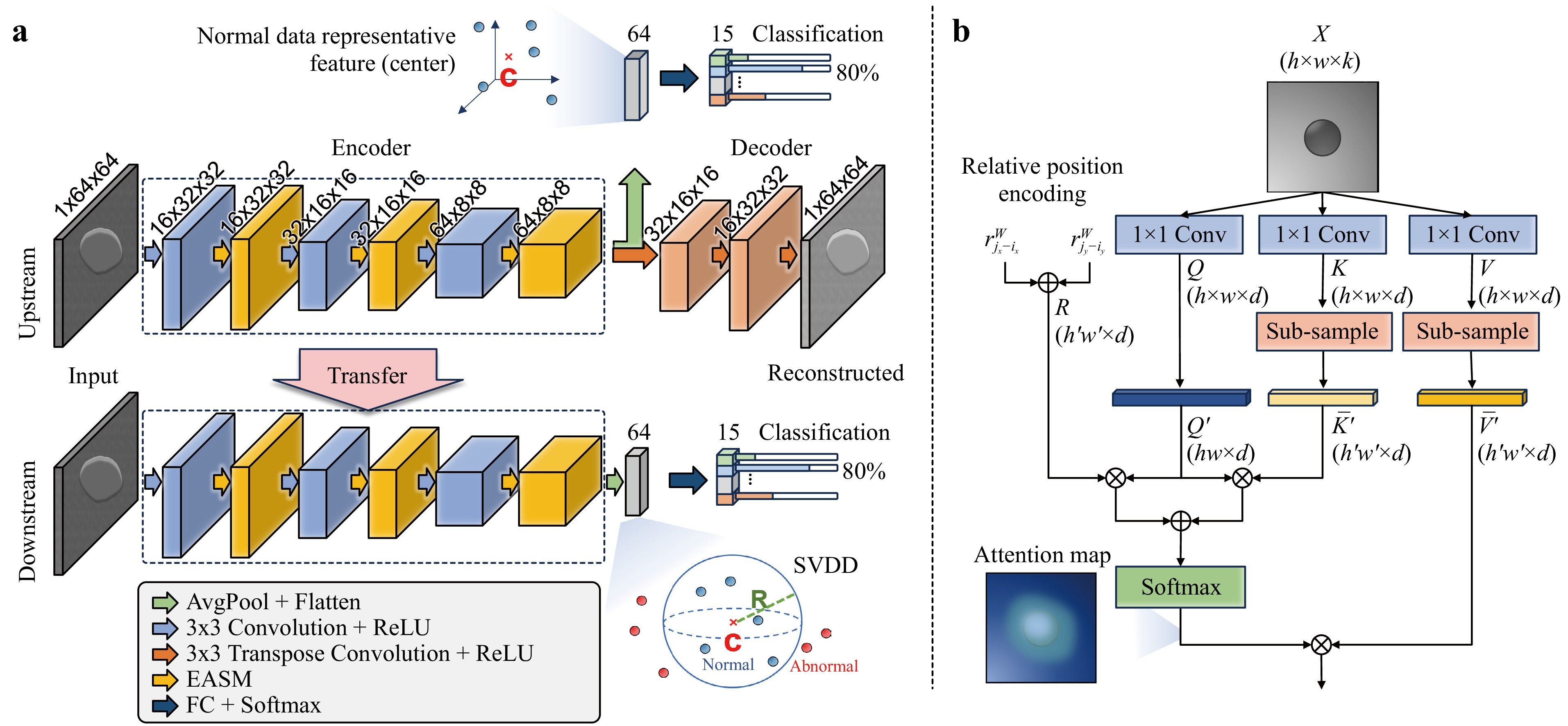
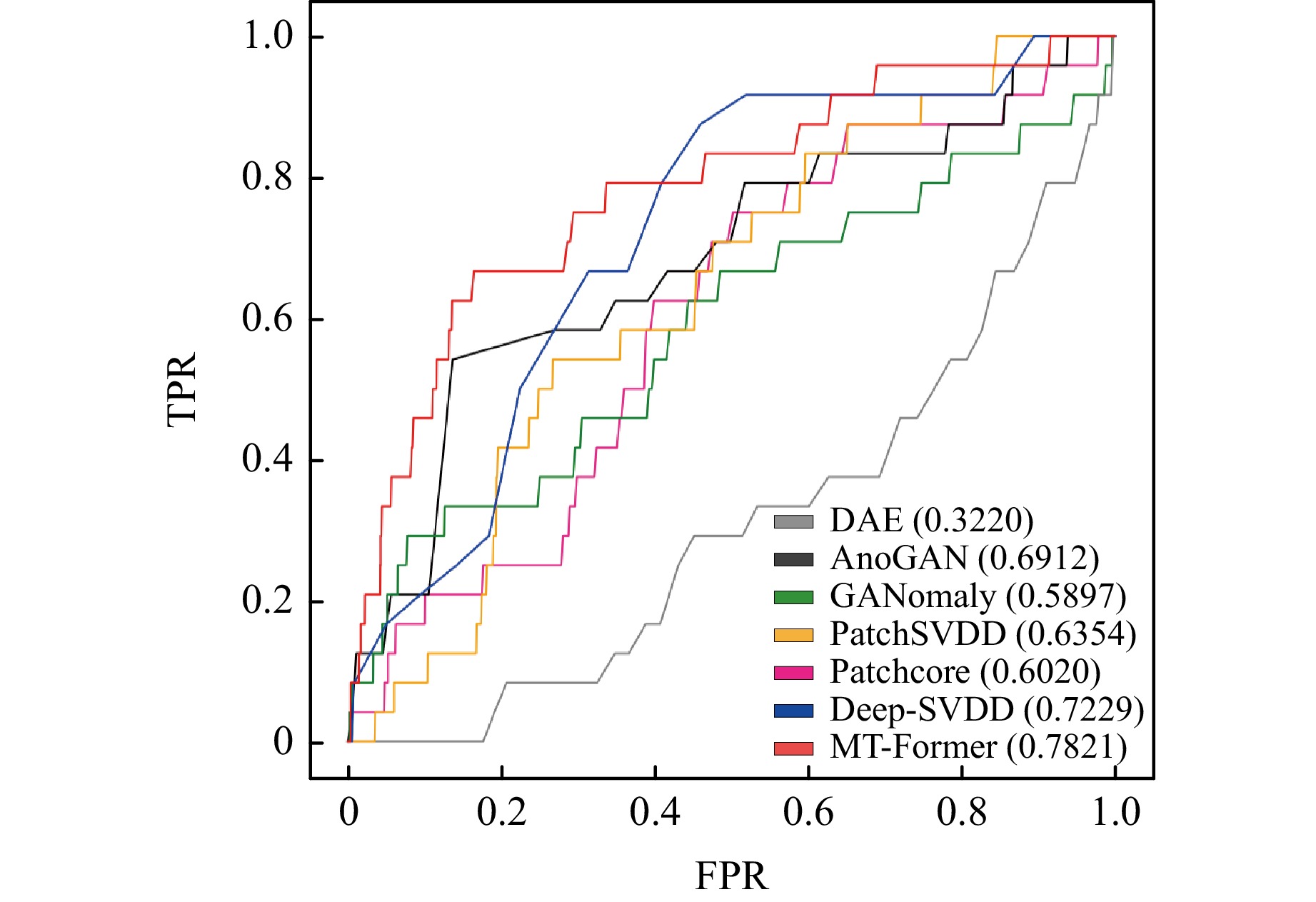
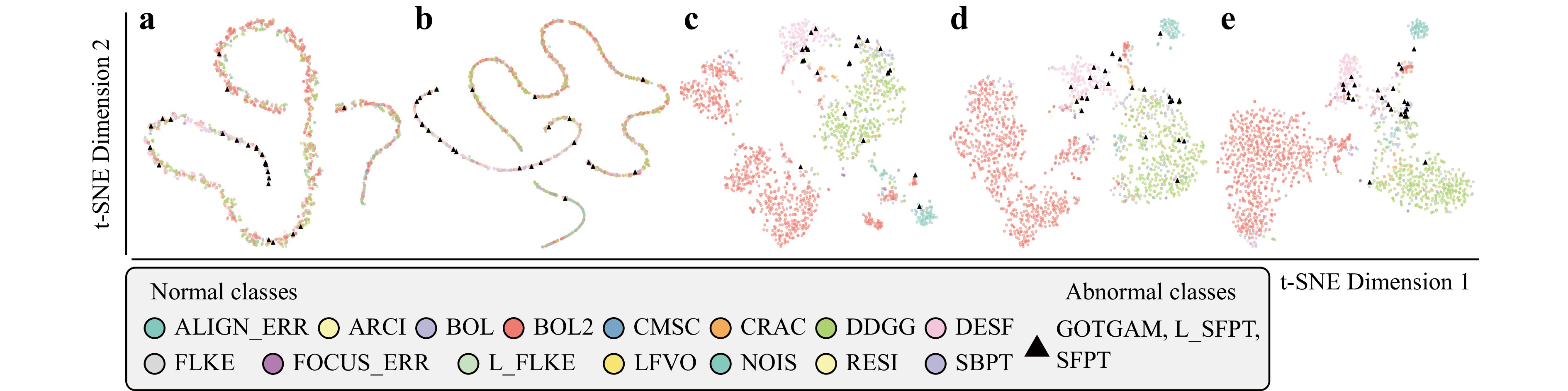
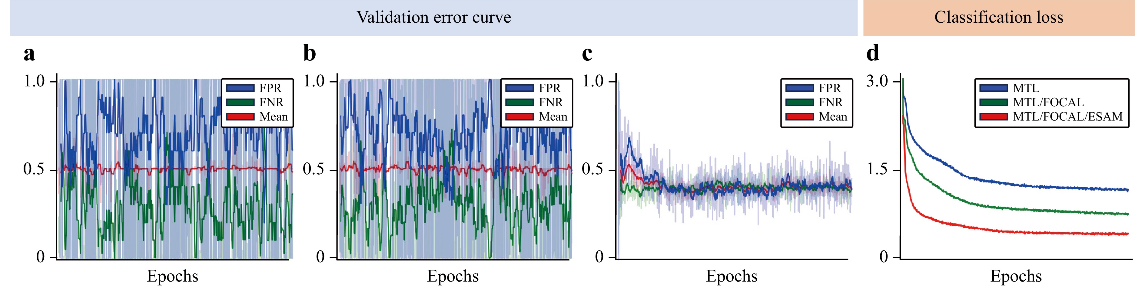
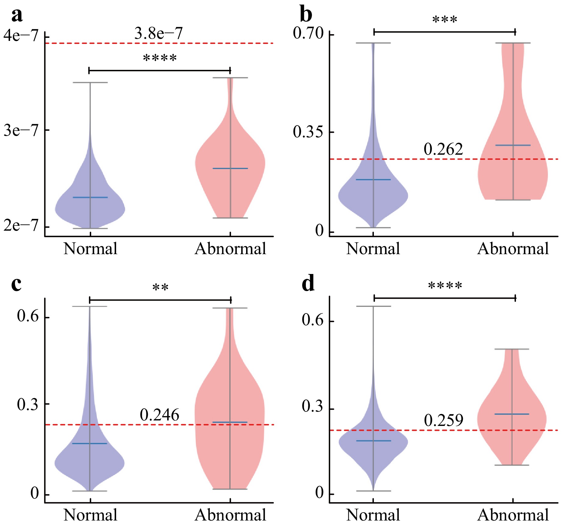
Defect inspection is critical in semiconductor manufacturing for product quality improvement at reduced production costs. A whole new manufacturing process is often associated with a new set of defects that can cause serious damage to the manufacturing system. Therefore, classifying existing defects and new defects provides crucial clues to fix the issue in the newly introduced manufacturing process. We present a multi-task hybrid transformer (MT-former) that distinguishes novel defects from the known defects in electron microscope images of semiconductors. MT-former consists of upstream and downstream training stages. In the upstream stage, an encoder of a hybrid transformer is trained by solving both classification and reconstruction tasks for the existing defects. In the downstream stage, the shared encoder is fine-tuned by simultaneously learning the classification as well as a deep support vector domain description (Deep-SVDD) to detect the new defects among the existing ones. With focal loss, we also design a hybrid-transformer using convolutional and an efficient self-attention module. Our model is evaluated on real-world data from SK Hynix and on publicly available data from magnetic tile defects and HAM10000. For SK Hynix data, MT-former achieved higher AUC as compared with a Deep-SVDD model, by 8.19% for anomaly detection and by 9.59% for classifying the existing classes. Furthermore, the best AUC (magnetic tile defect 67.9%, HAM10000 70.73%) on the public dataset achieved with the proposed model implies that MT-former would be a useful model for classifying the new types of defects from the existing ones.

Published. 2025, 6(2)
: 319-332
doi: 10.37188/lam.2025.040
This study proposes a novel heterodyne grating interferometer designed to meet the multi-dimensional atomic-level measurement demands of next-generation lithography systems and large-scale atomic-level manufacturing. By utilizing a dual-frequency laser source, the interferometer enables simultaneous three-degree-of-freedom (3-DOF) displacement measurements. Key innovations include a compact, zero dead-zone optical path architecture, which enhances measurement robustness by minimizing sensitivity to laser source instabilities and atmospheric refractive index fluctuations. In addition, we present a systematic crosstalk error analysis, coupled with a corresponding compensation algorithm, effectively reducing crosstalk-induced errors to below 5%. Experimental evaluation of the 90 × 90 × 40 mm3 prototype demonstrates outstanding performance metrics: sub-nanometer resolutions (0.25 nm for X/Y-axes, 0.3 nm for Z-axis), superior linearity coefficients (6.9 × 10⁻⁵, 8.1 × 10⁻⁵, 16.2 × 10⁻⁵ for X-, Y-, and Z-axes, respectively), high repeatability (0.8 nm@1000 nm for all axes), exceptional long-term stability (20 nm XY-plane drift, 60 nm Z-axis drift over 1000 s), and practical measurement ranges exceeding 10 mm in-plane and 2 mm axially. Comparative analysis with state-of-the-art sensors demonstrates significant advantages in measurement precision, system integration, and multi-axis capability. This advancement highlights excellent potential for applications in integrated circuit fabrication, atomic-scale manufacturing, and ultra-precision metrology for aerospace systems.


Published. 2025, 6(2)
: 333-357
doi: 10.37188/lam.2025.022
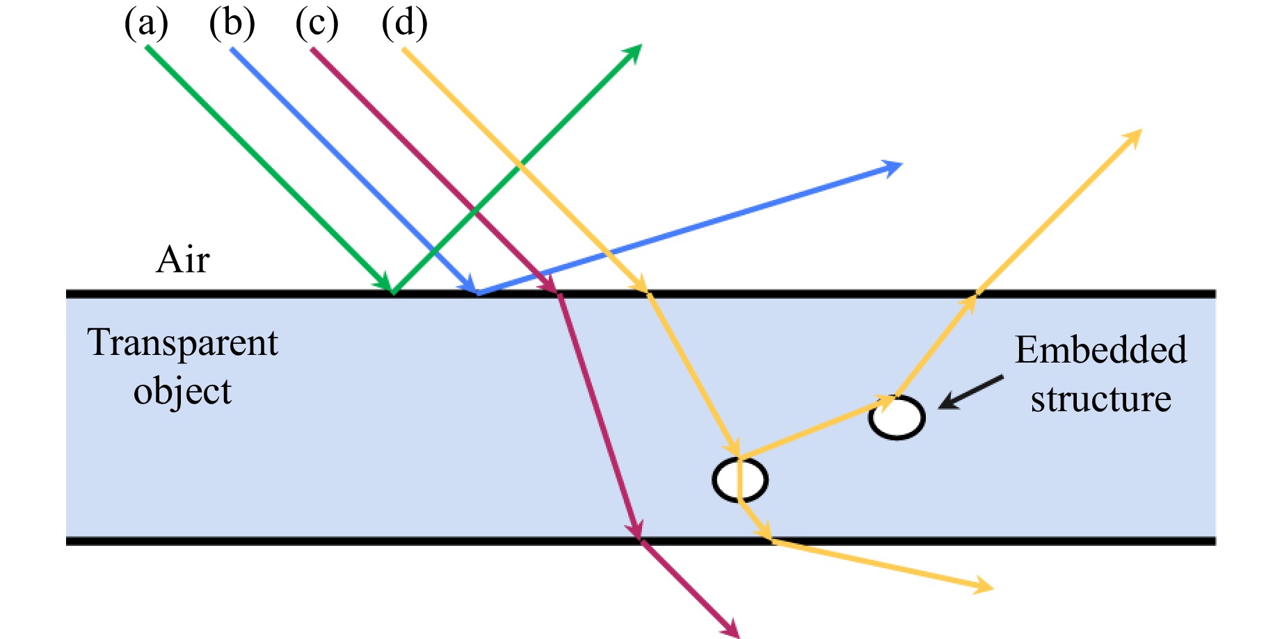
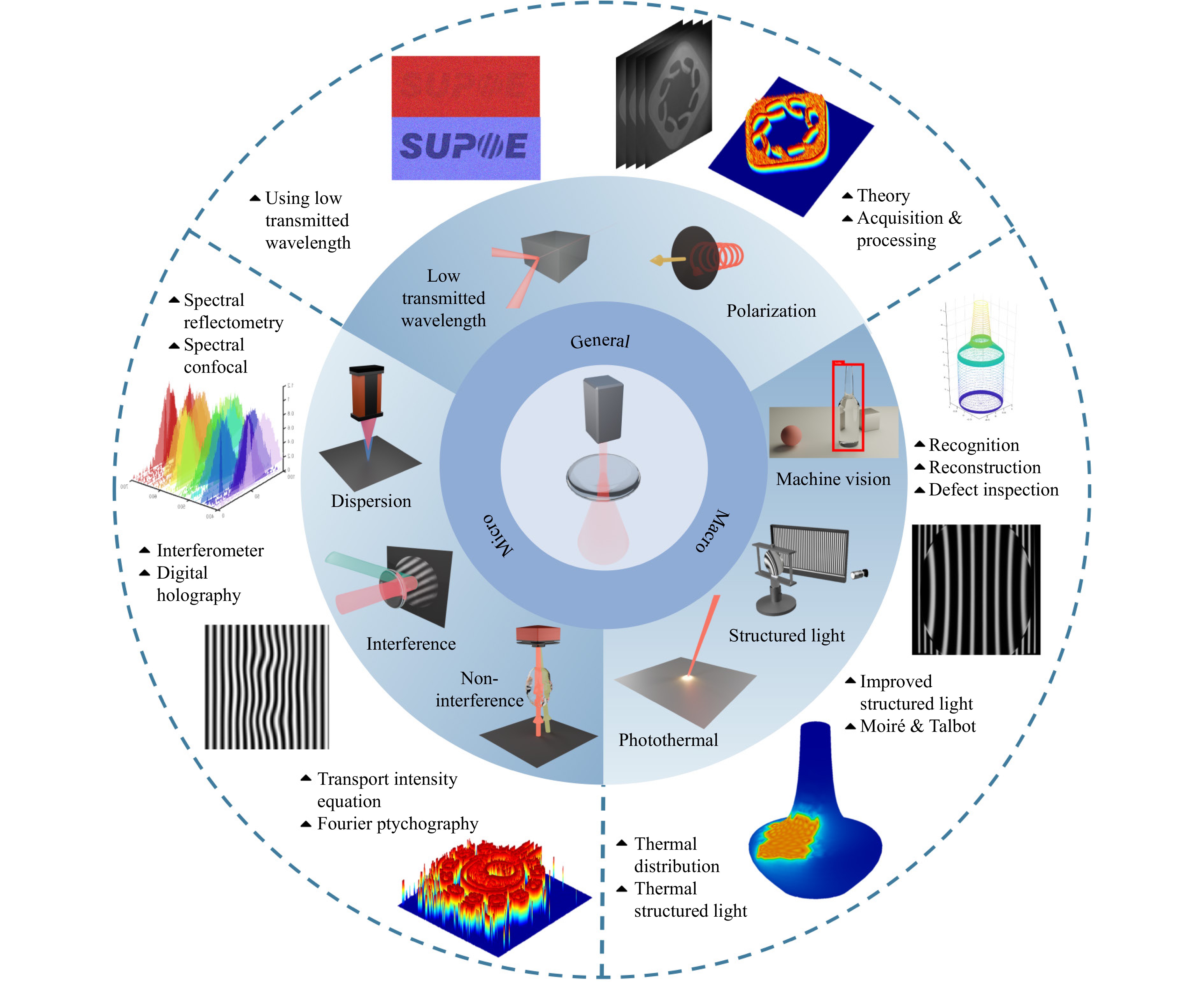
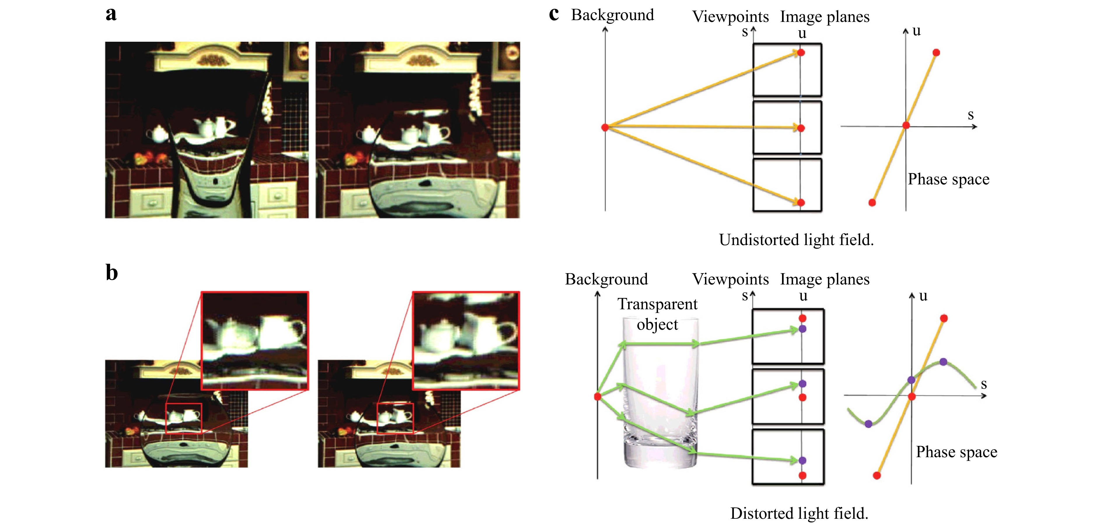
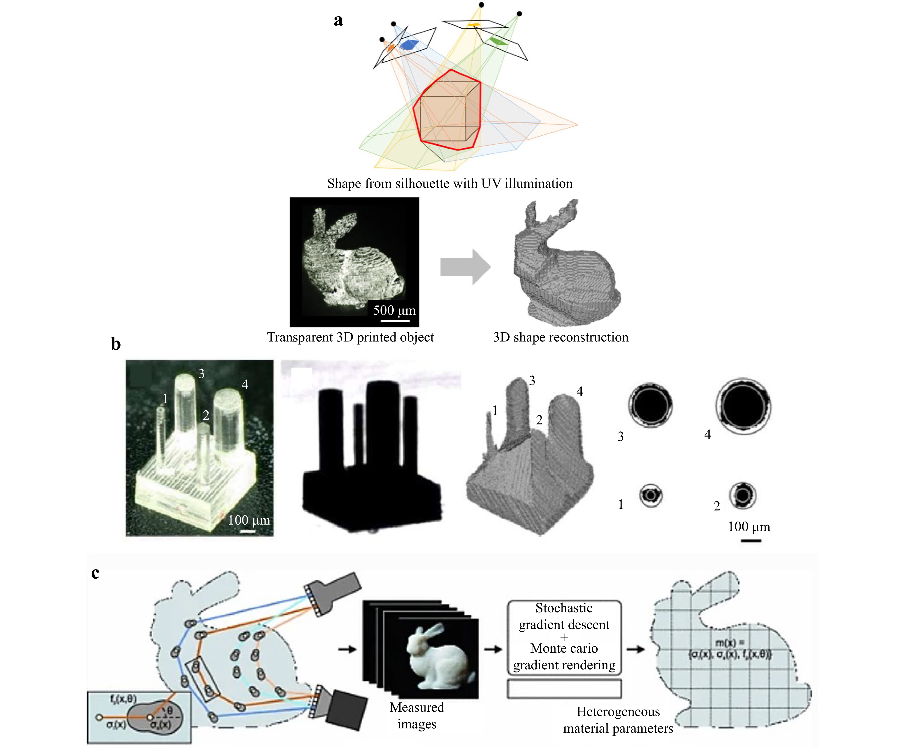
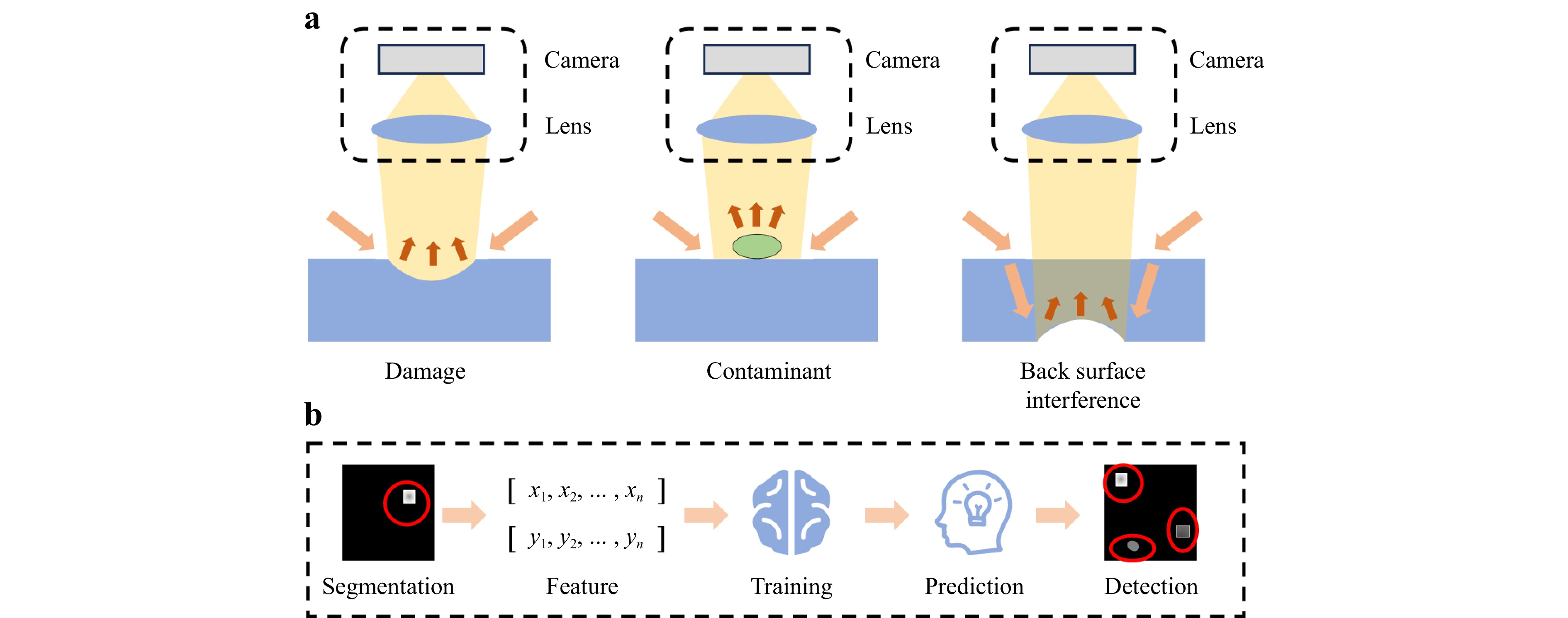
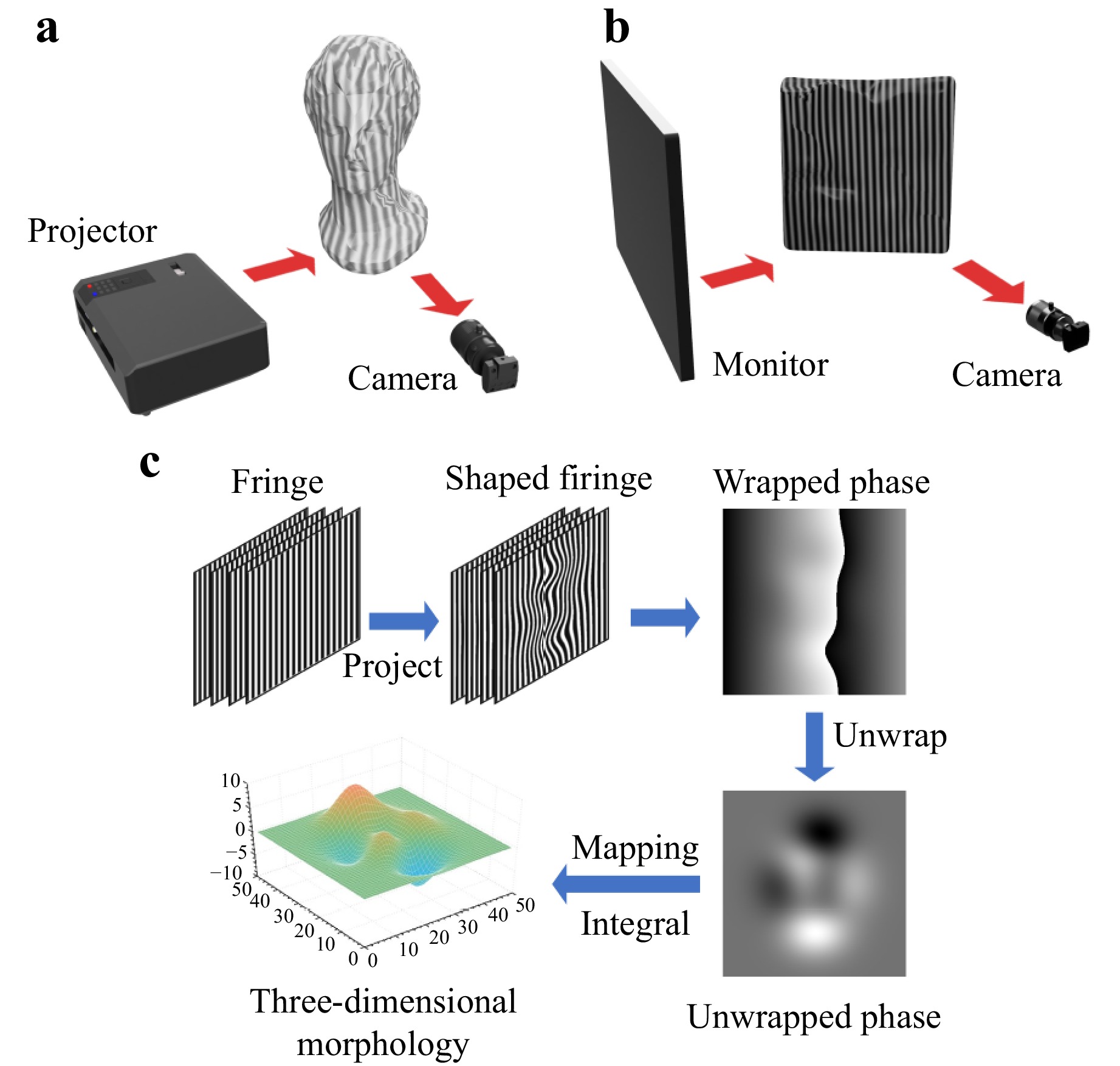
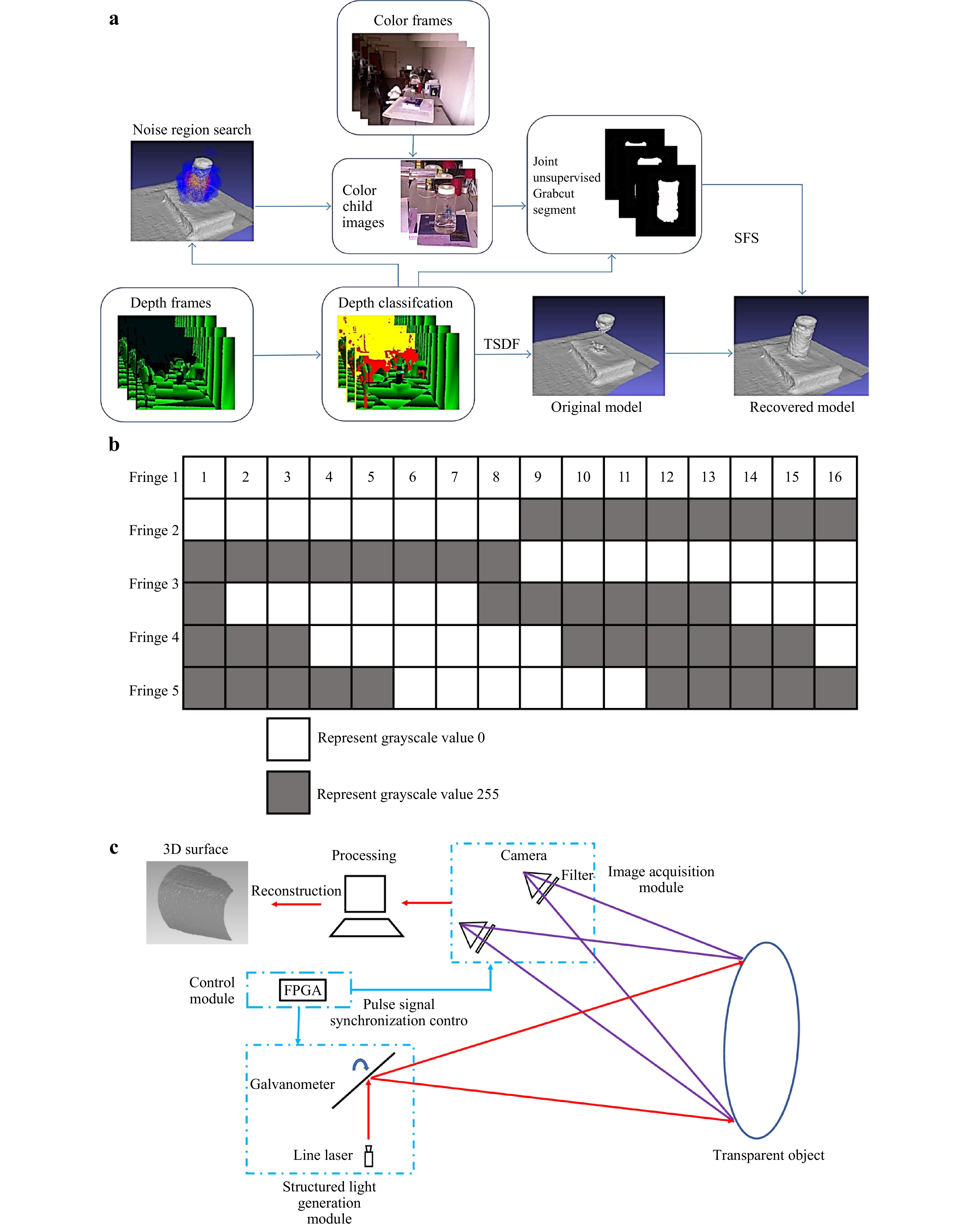
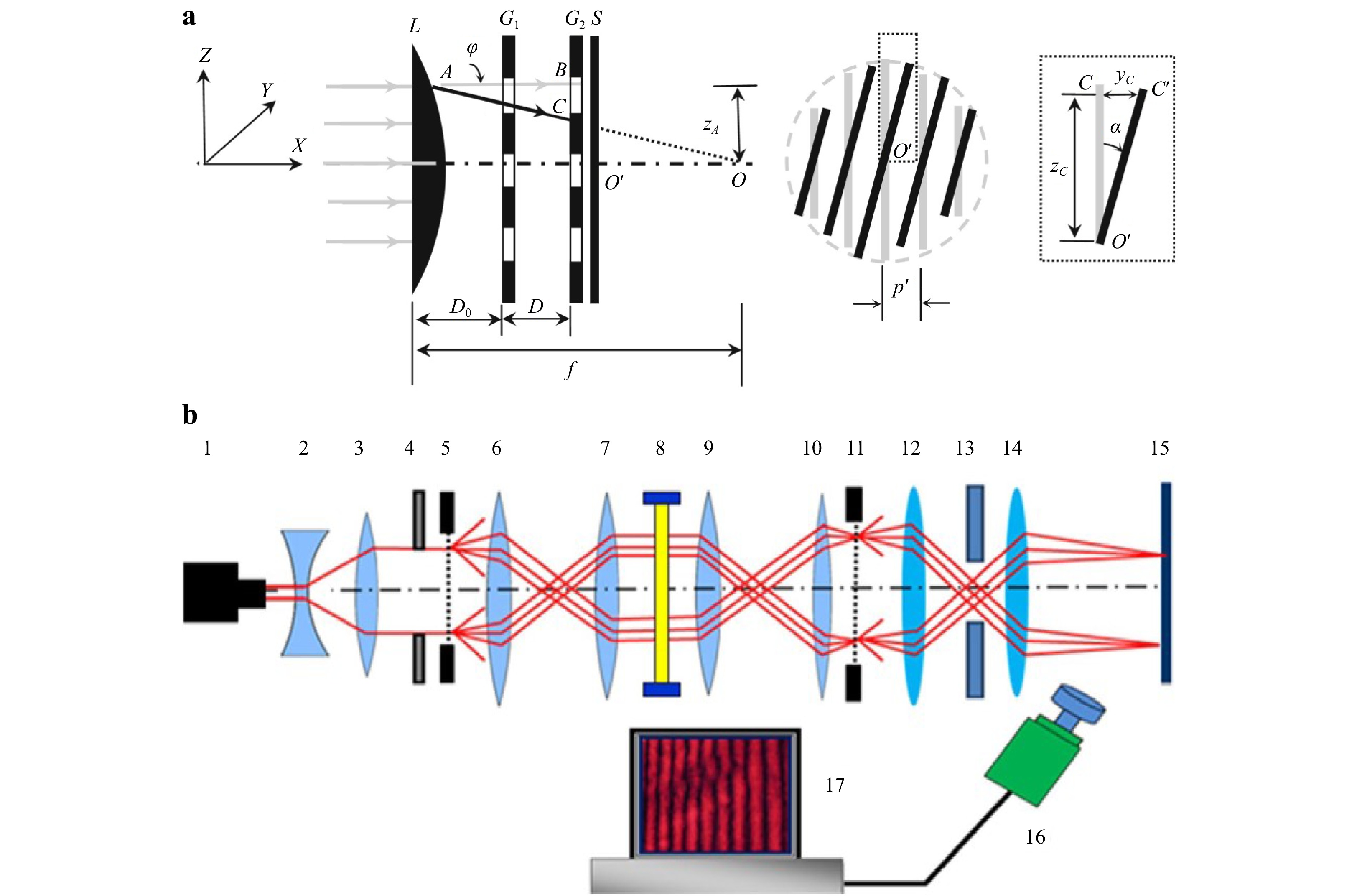
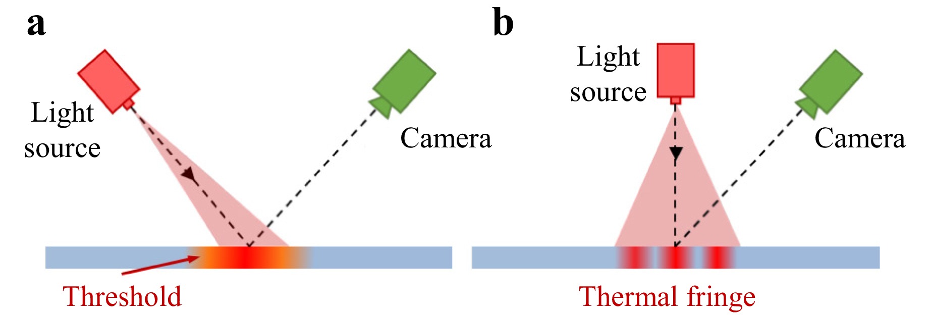
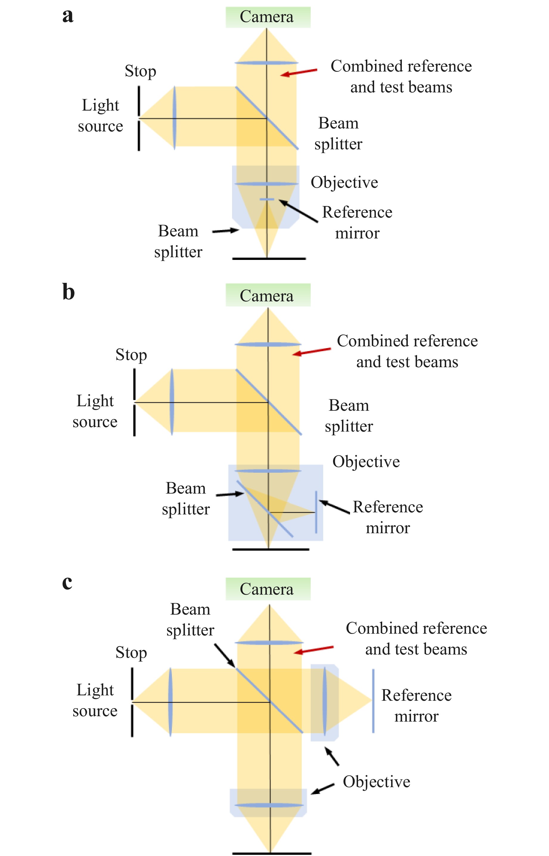
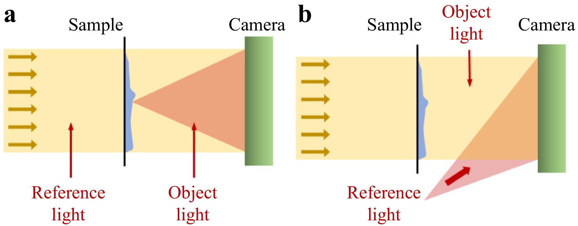
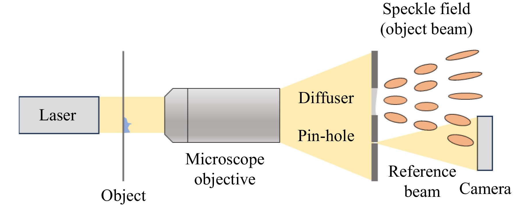
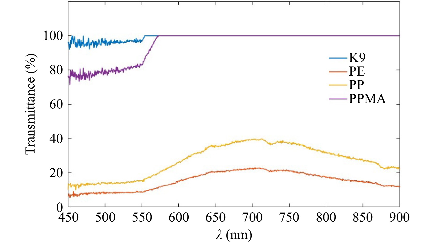
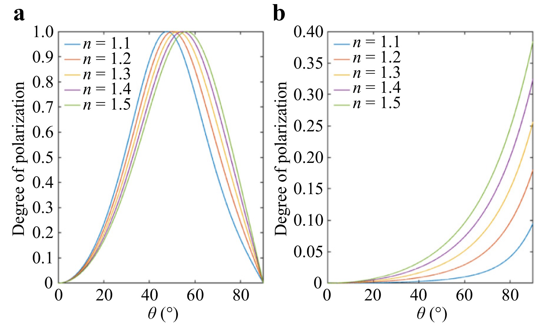
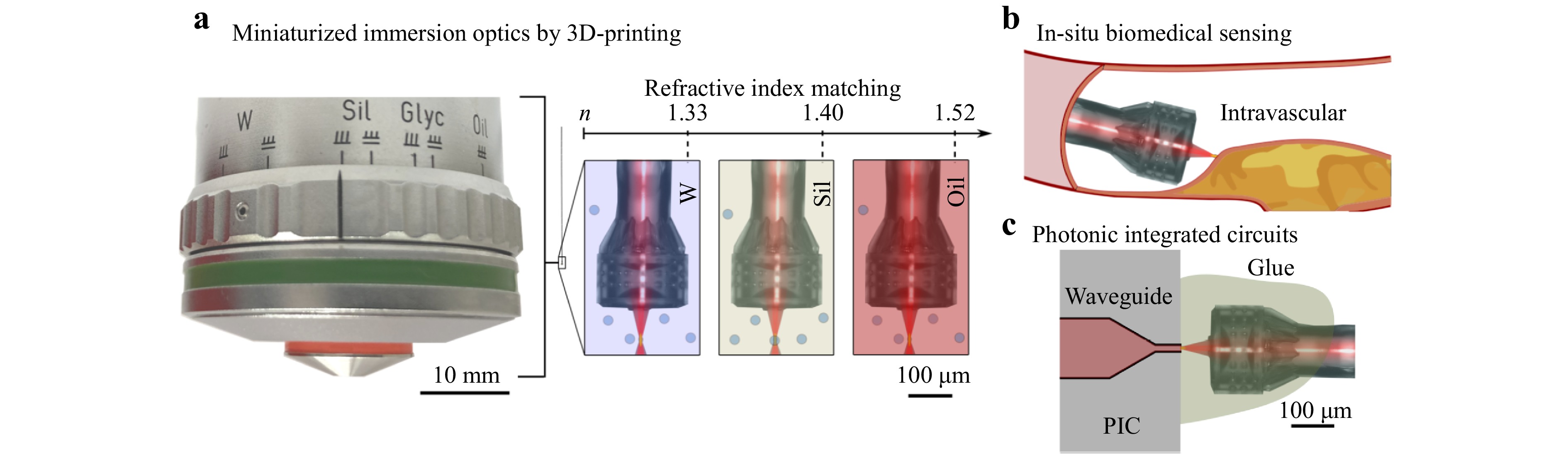
Transparent objects are widely used in various fields, leading to increasing demand for methods of measuring them. However, the measurement of such objects has always been challenging owing to the intricate refraction and reflection phenomena they exhibit. Given that traditional contact measurement methods can damage transparent objects, the use of non-destructive measurement techniques, particularly those based on optical principles, is considered preferable. As a result, various non-destructive measurement methods have been developed for transparent objects by leveraging the unique characteristics of light, and a comprehensive review is imperative for exploring these innovative methods and their potential applications. This review accordingly begins by elucidating the necessity of measuring transparent objects and exploring the concept of transparency. Next, an overview of various non-destructive optical measurement techniques spanning macro-, micro-, and general-scale applications is presented, followed by a discussion of their respective advantages and limitations. Finally, the paper concludes by outlining future directions for potential advancements in the field. This review is expected to serve as a valuable resource for newcomers in the field of transparent object measurement and assist researchers seeking to integrate these techniques into interdisciplinary studies.
Published. 2025, 6(2)
: 358-387
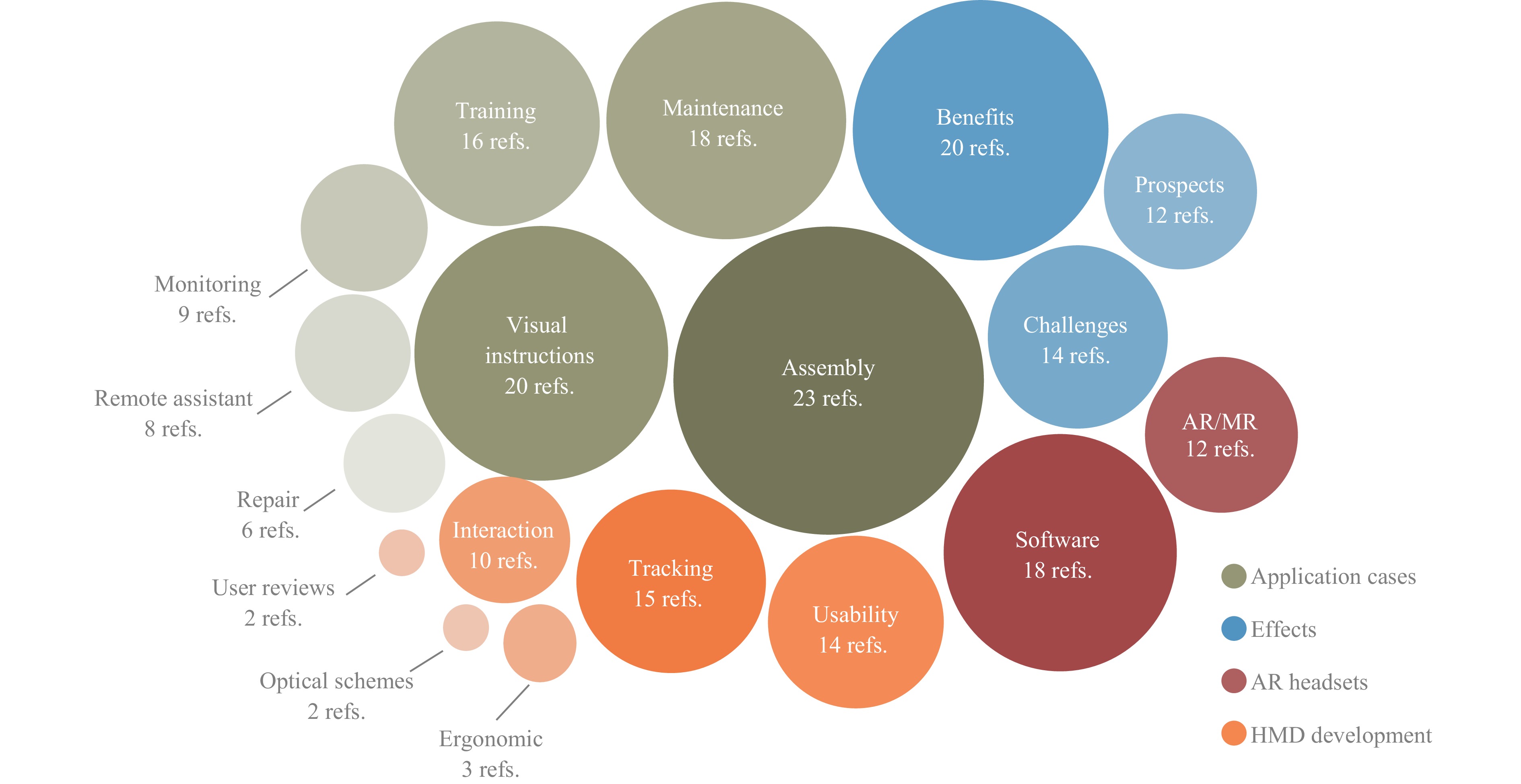
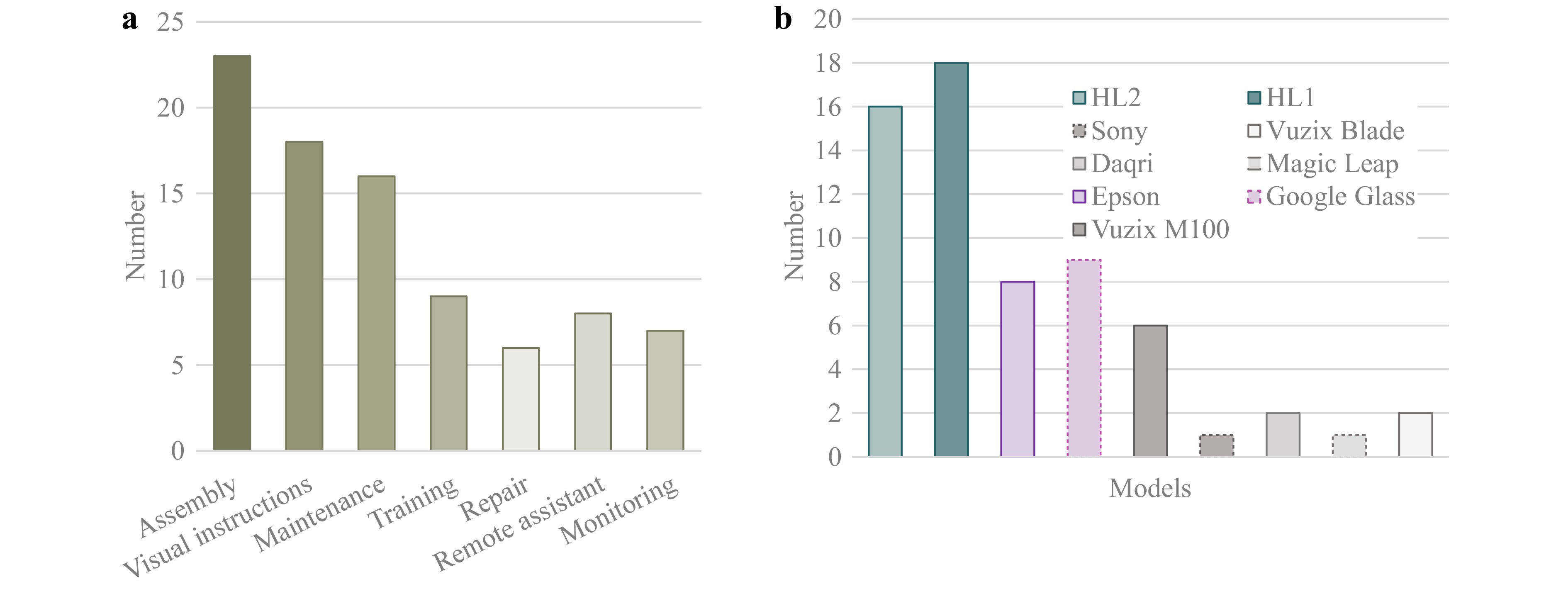
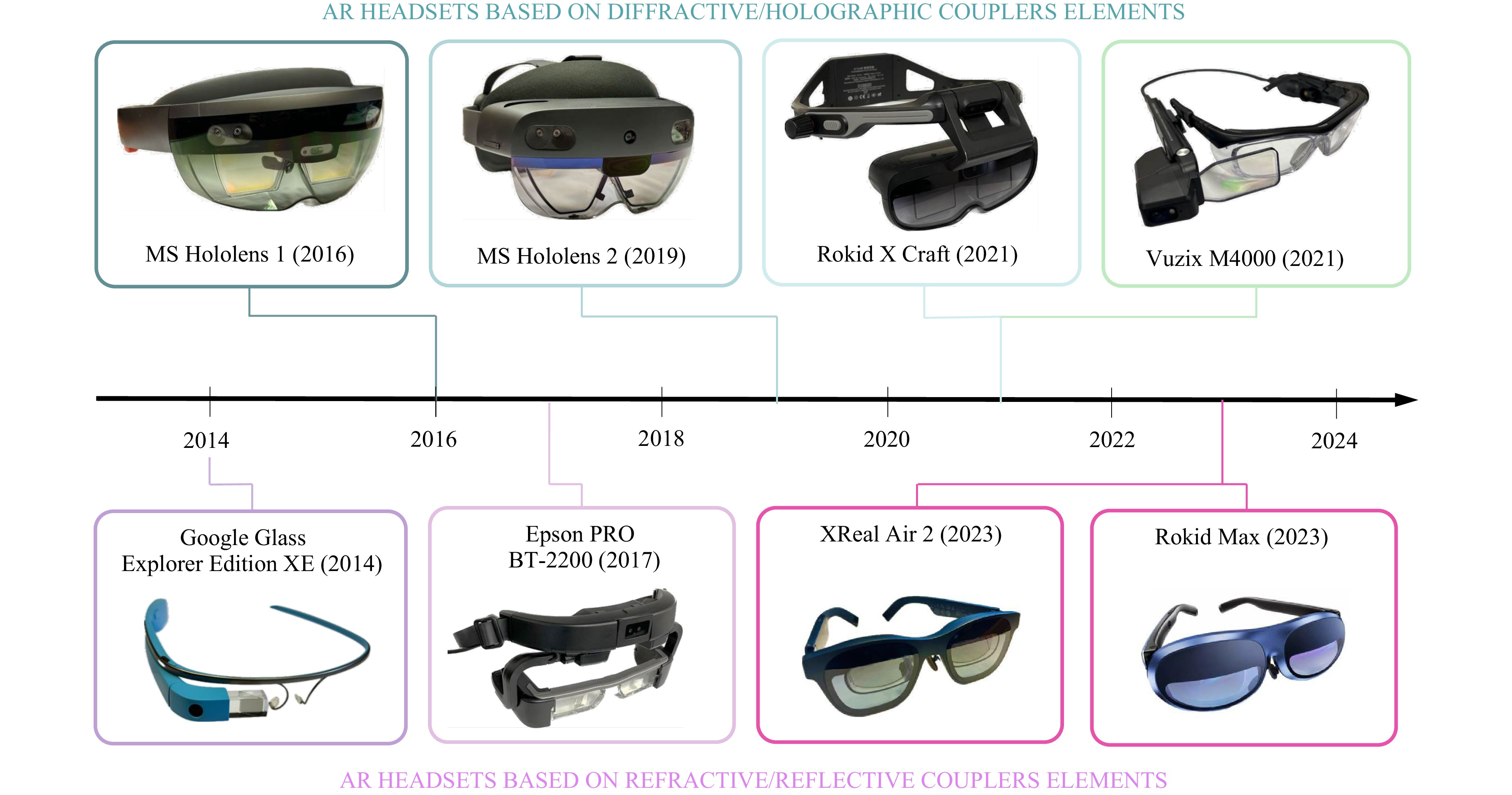
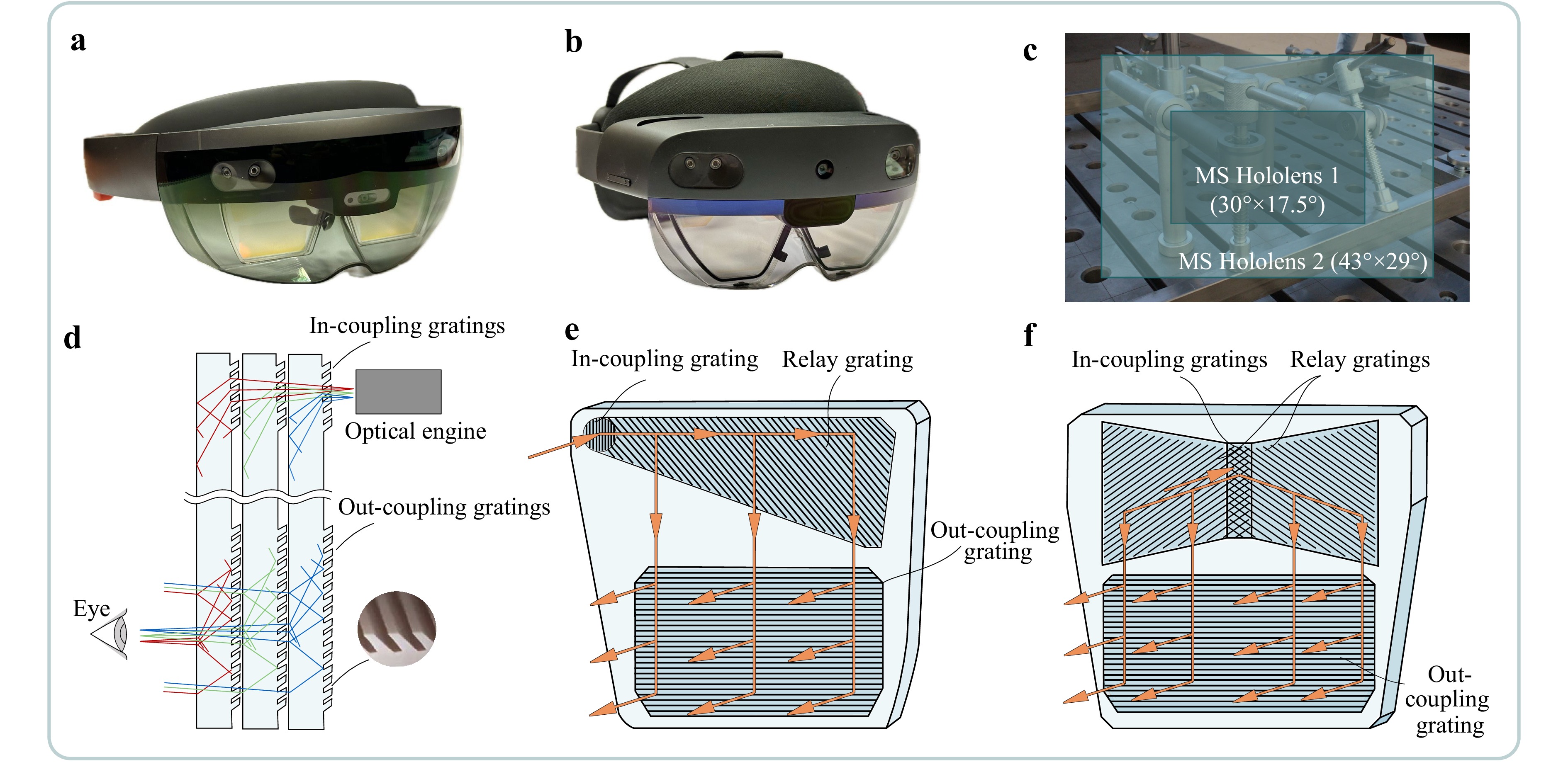
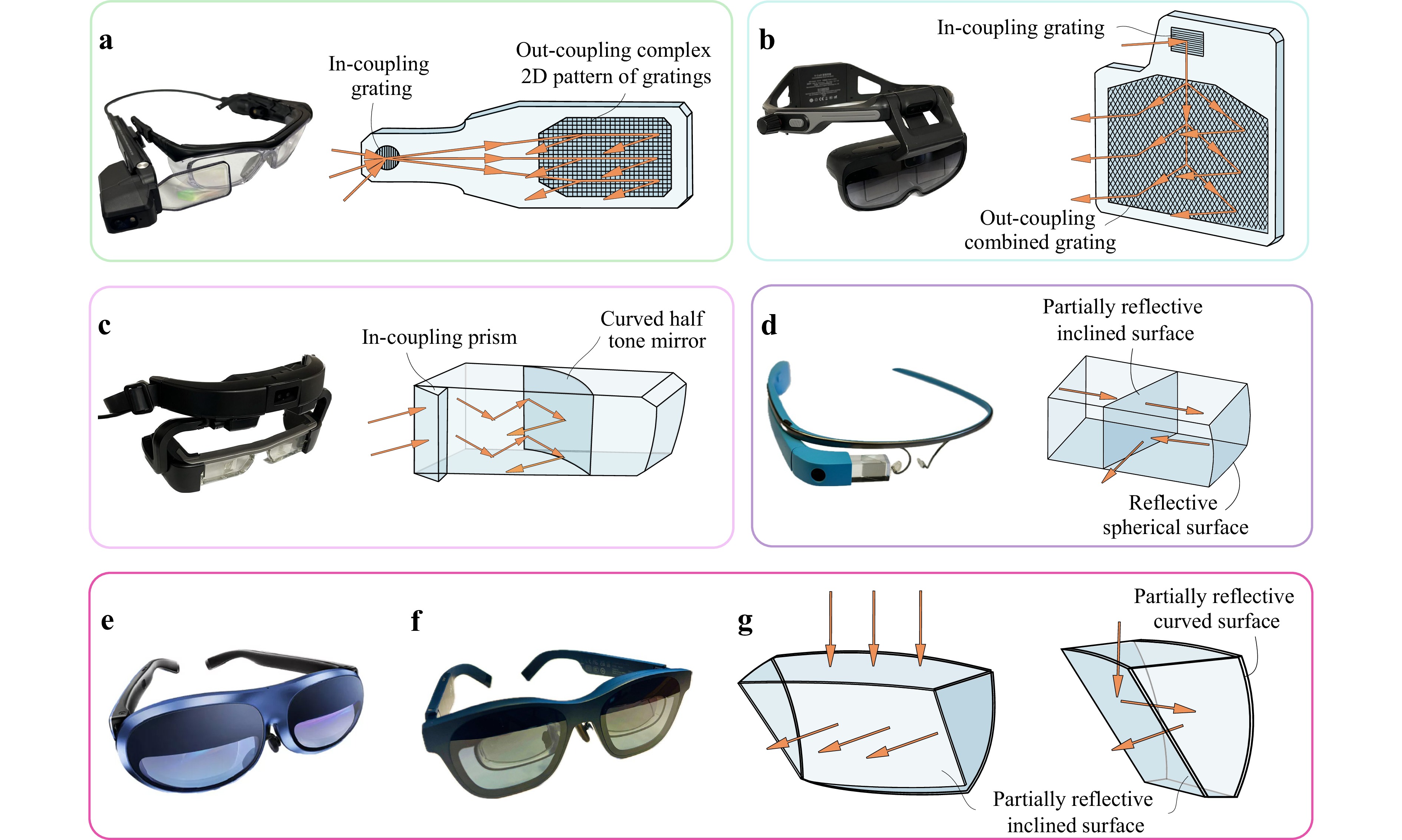
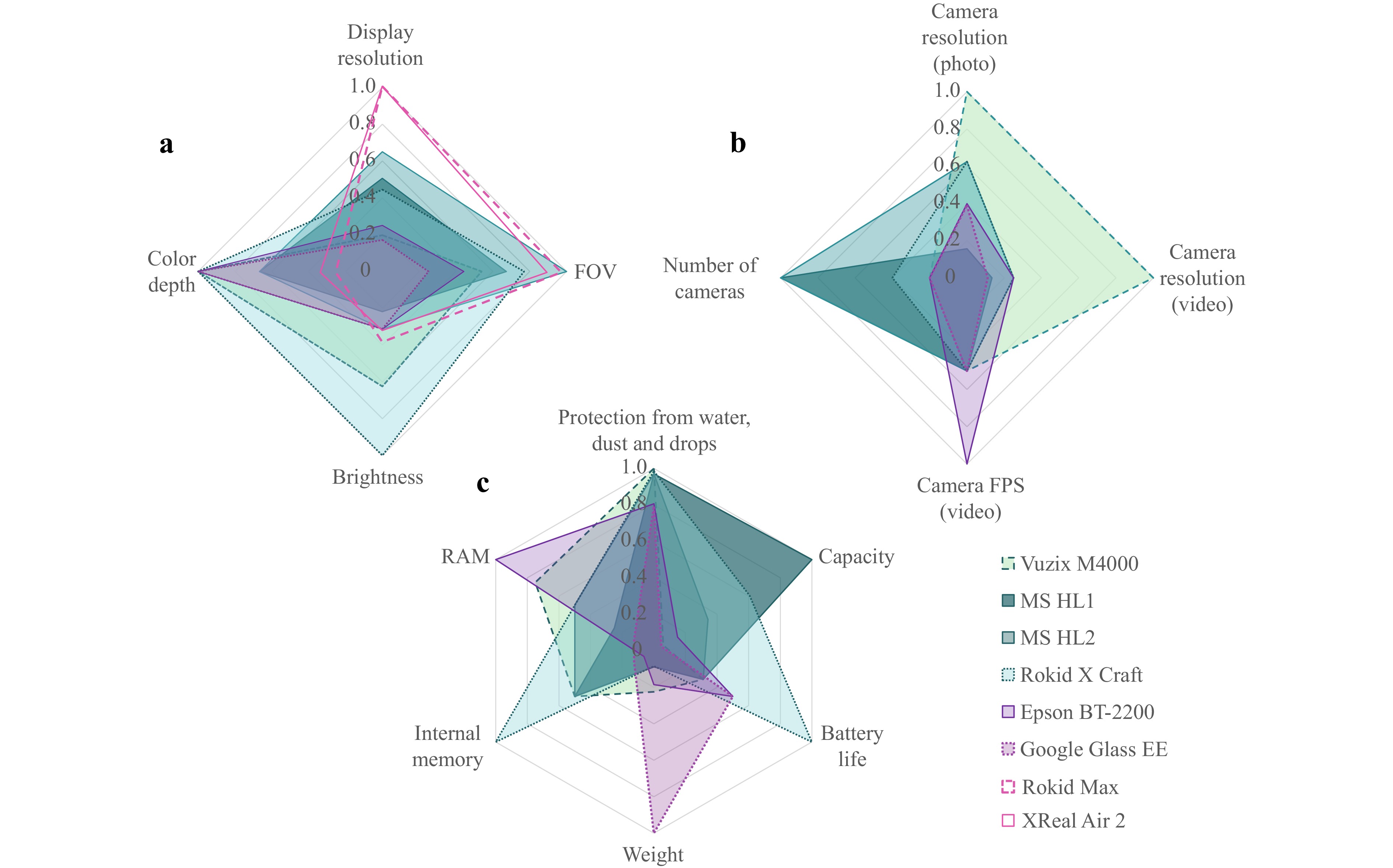
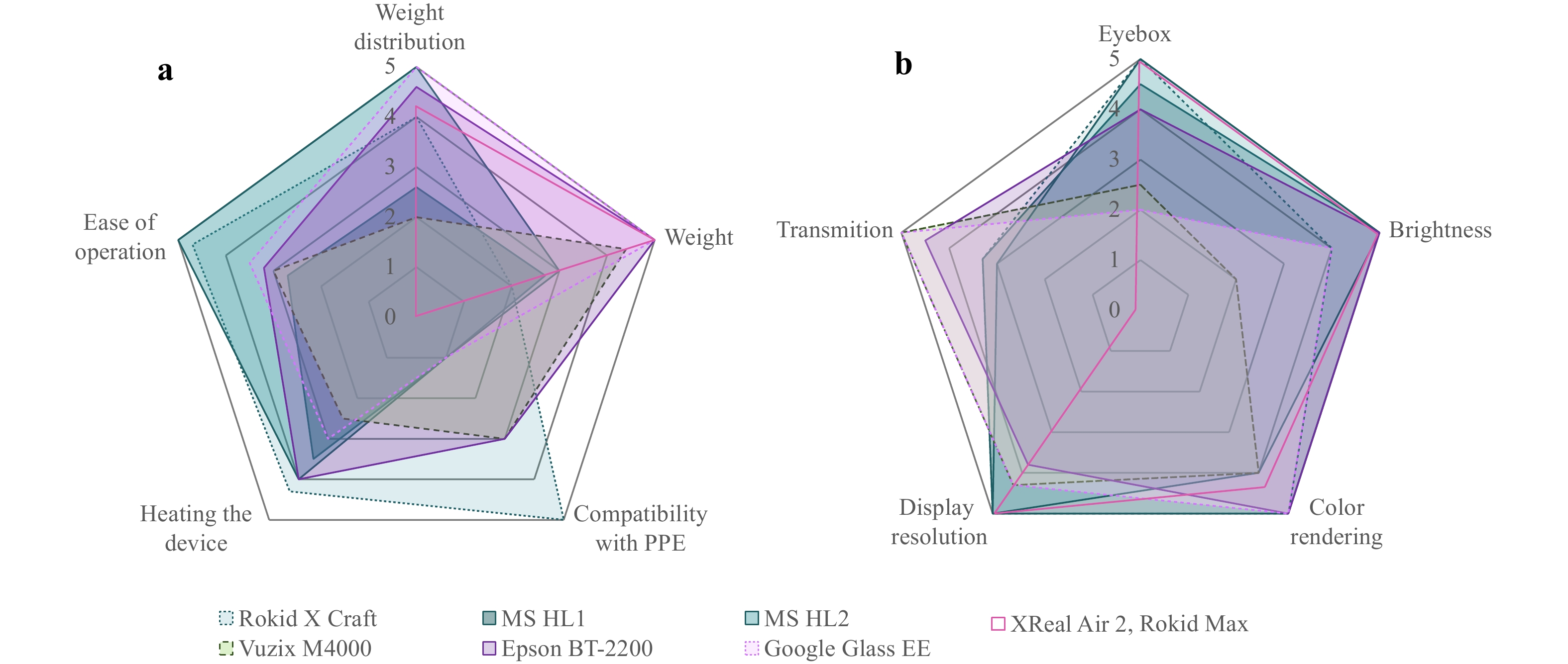
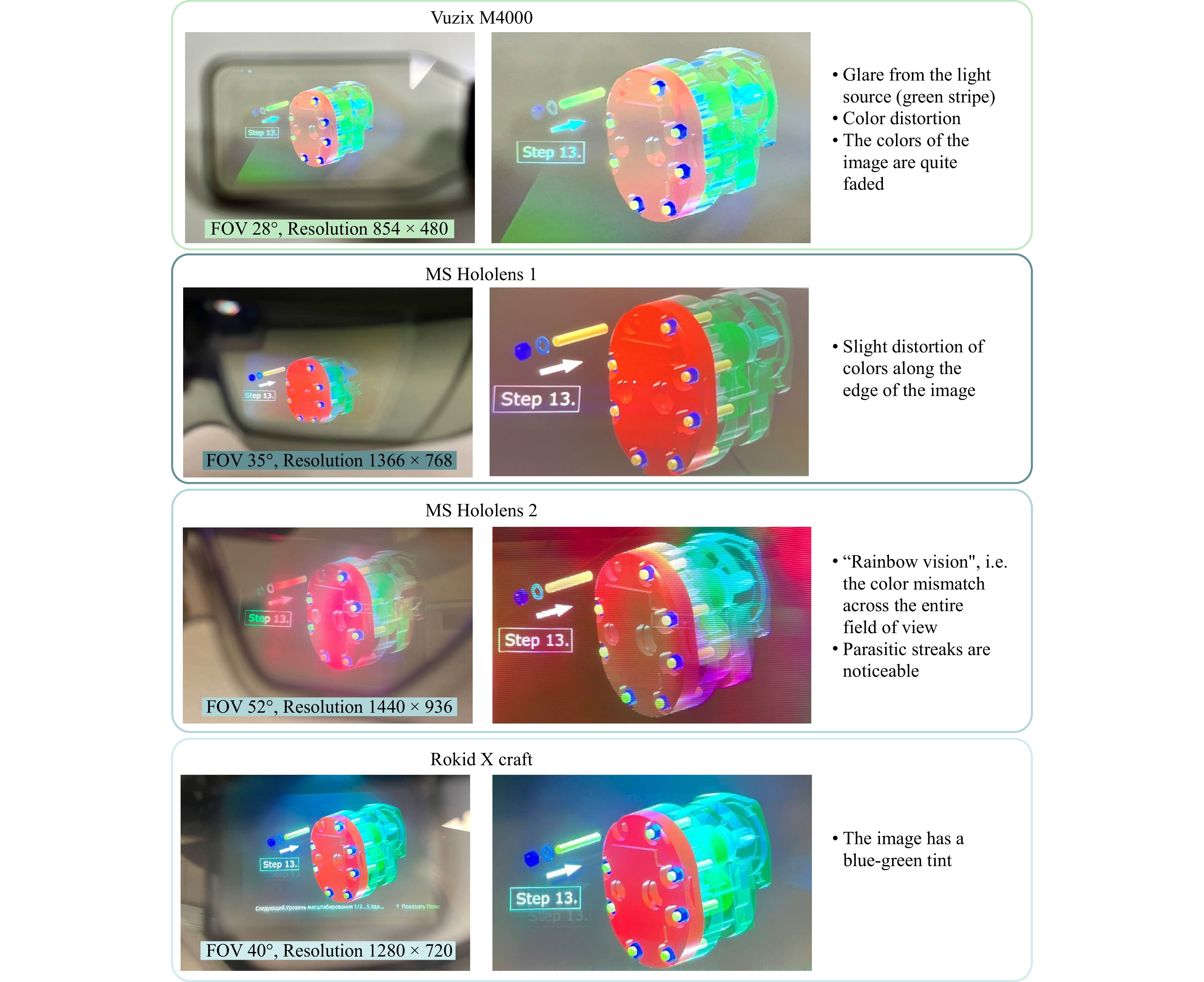
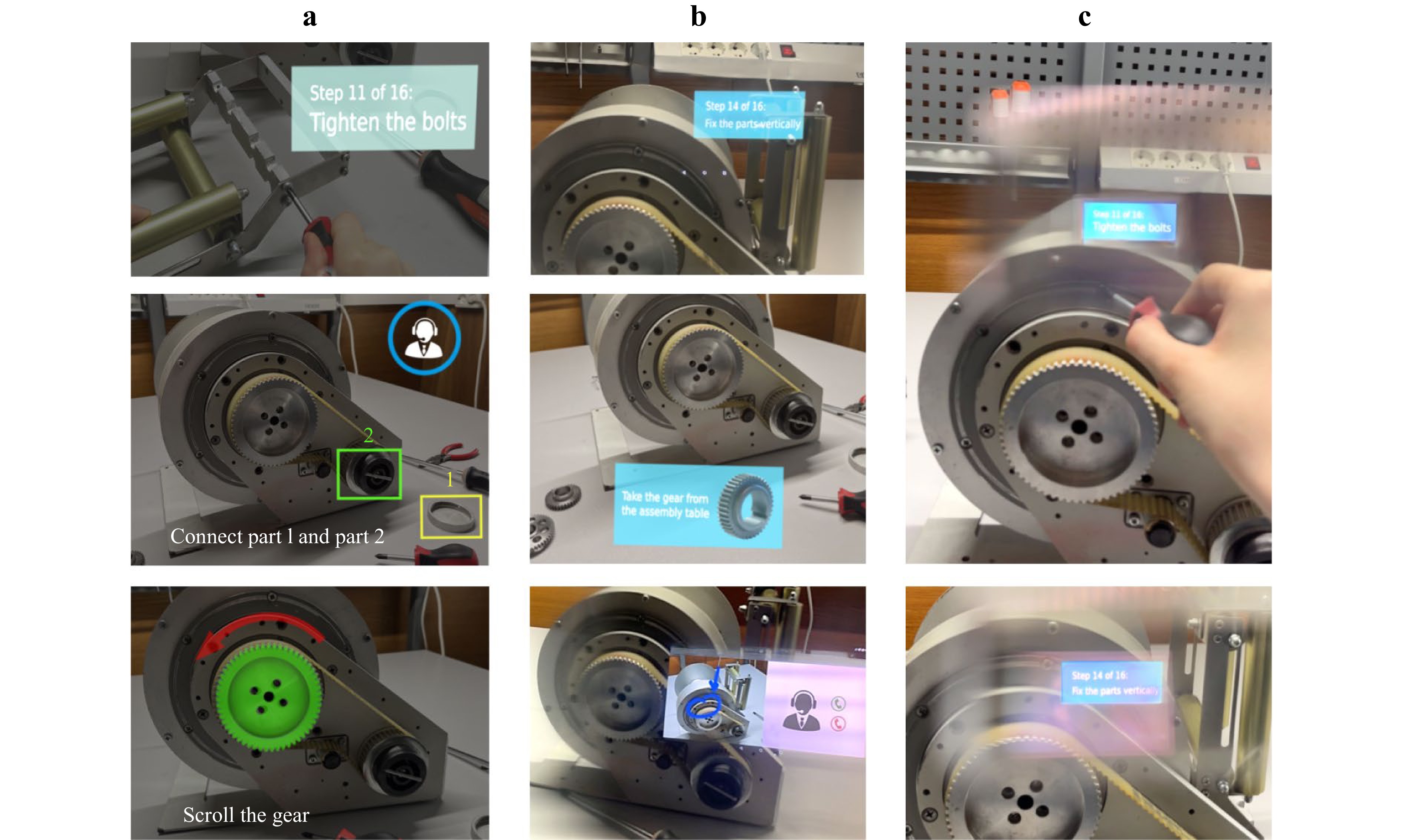
doi: 10.37188/lam.2025.023
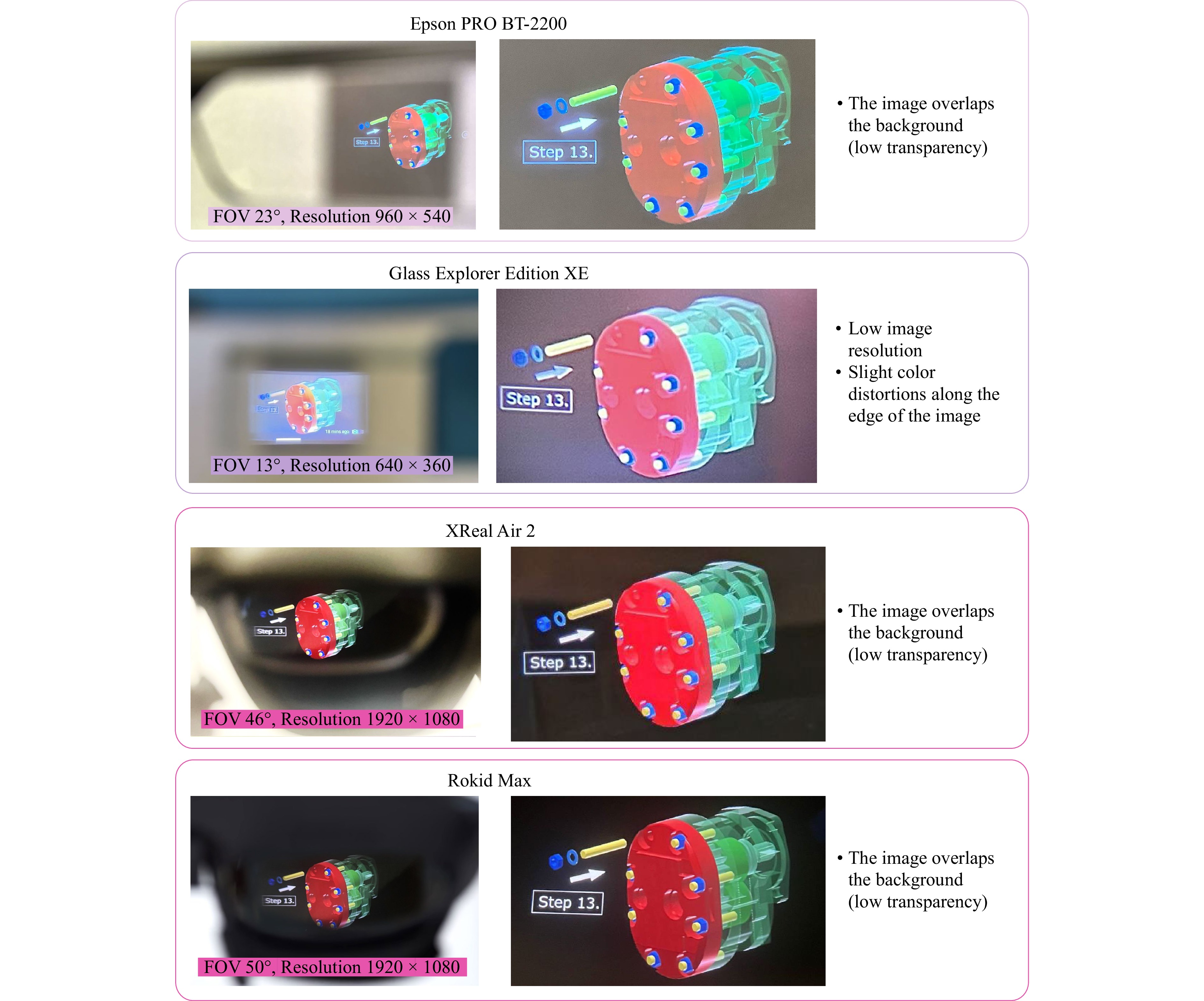
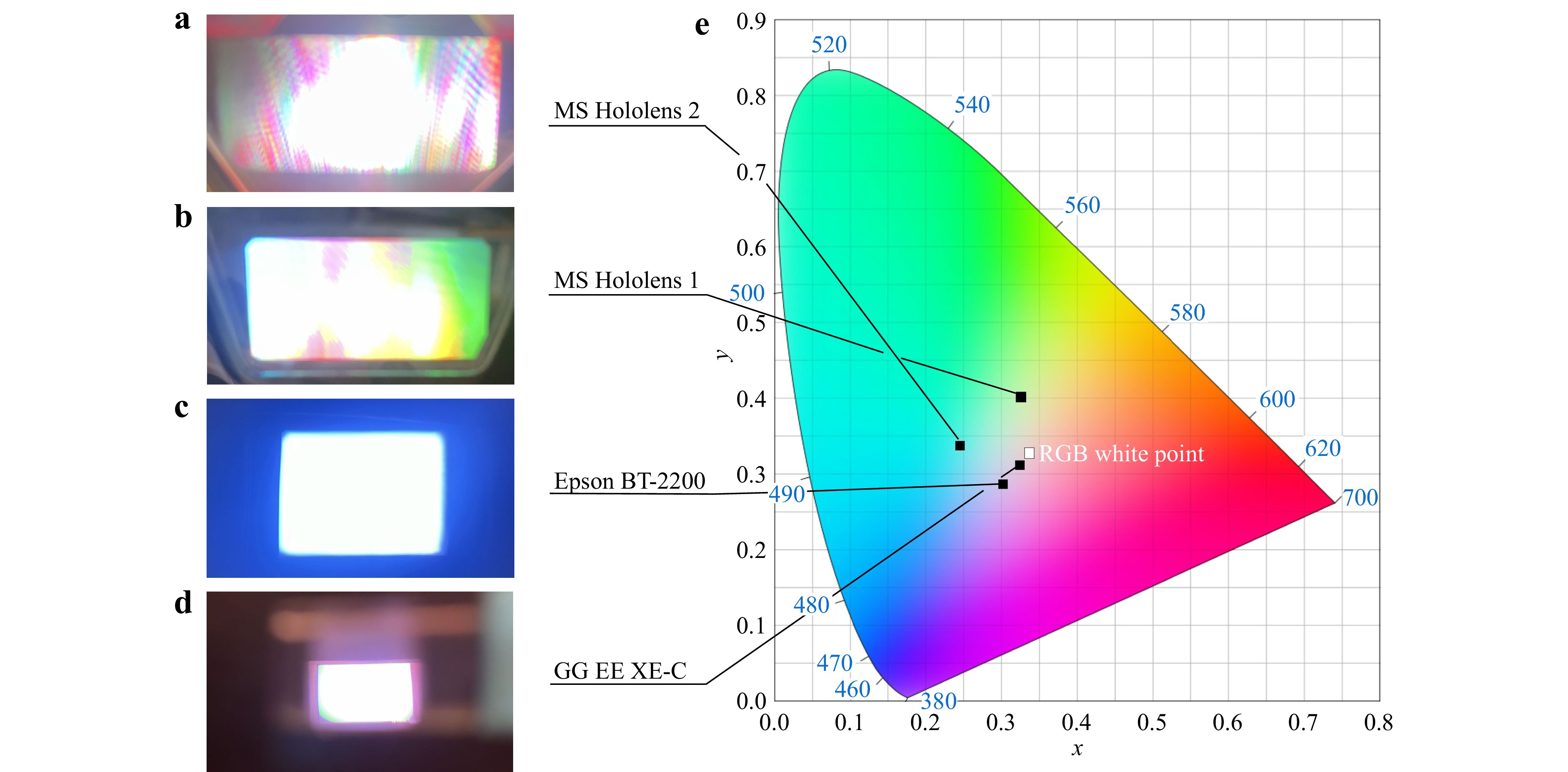
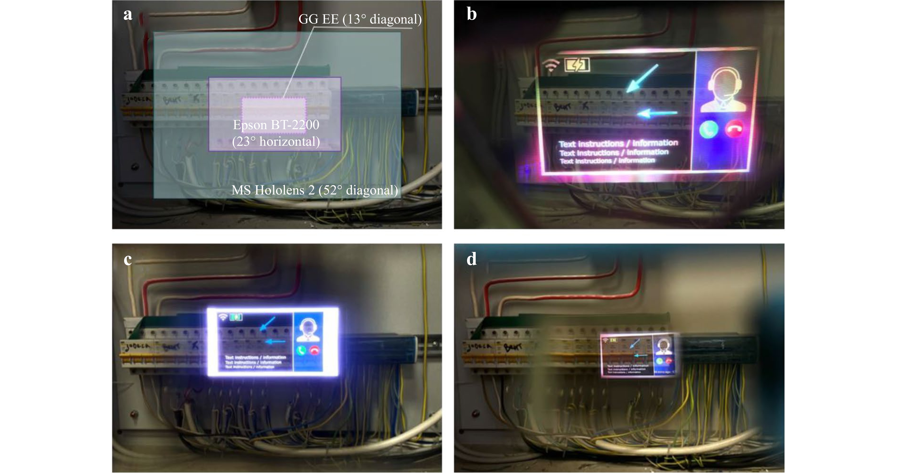
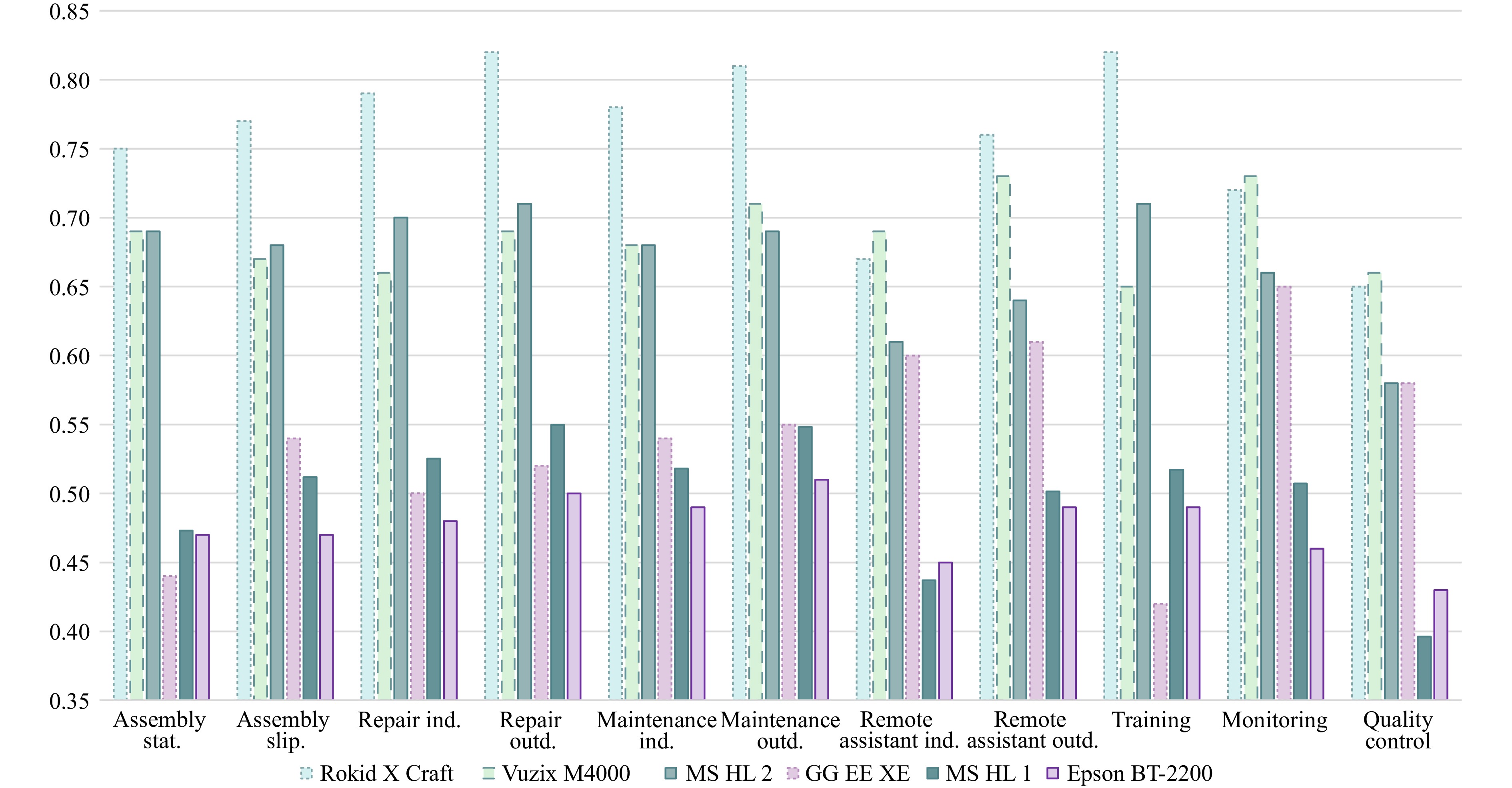
This review considers the modern industrial applications of augmented reality headsets. It draws upon a synthesis of information from open sources and press releases of companies, as well as the first-hand experiences of industry representatives. Furthermore, the research incorporates insights from both profile events and in-depth discussions with skilled professionals. A specific focus is placed on the ergonomic characteristics of headsets: image quality, user-friendliness, etc. To provide an objective evaluation of the various headsets, a metric has been proposed which is dependent on the specific application case. This enables a comprehensive comparison of the various devices in terms of their quantitative characteristics, which is of particular importance for the formation of a rapidly developing industry.

 Email
Email RSS
RSS