
2025 Vol. 6, No. 3
Published. 2025, 6(3)
: 399-401
doi: 10.37188/lam.2025.060
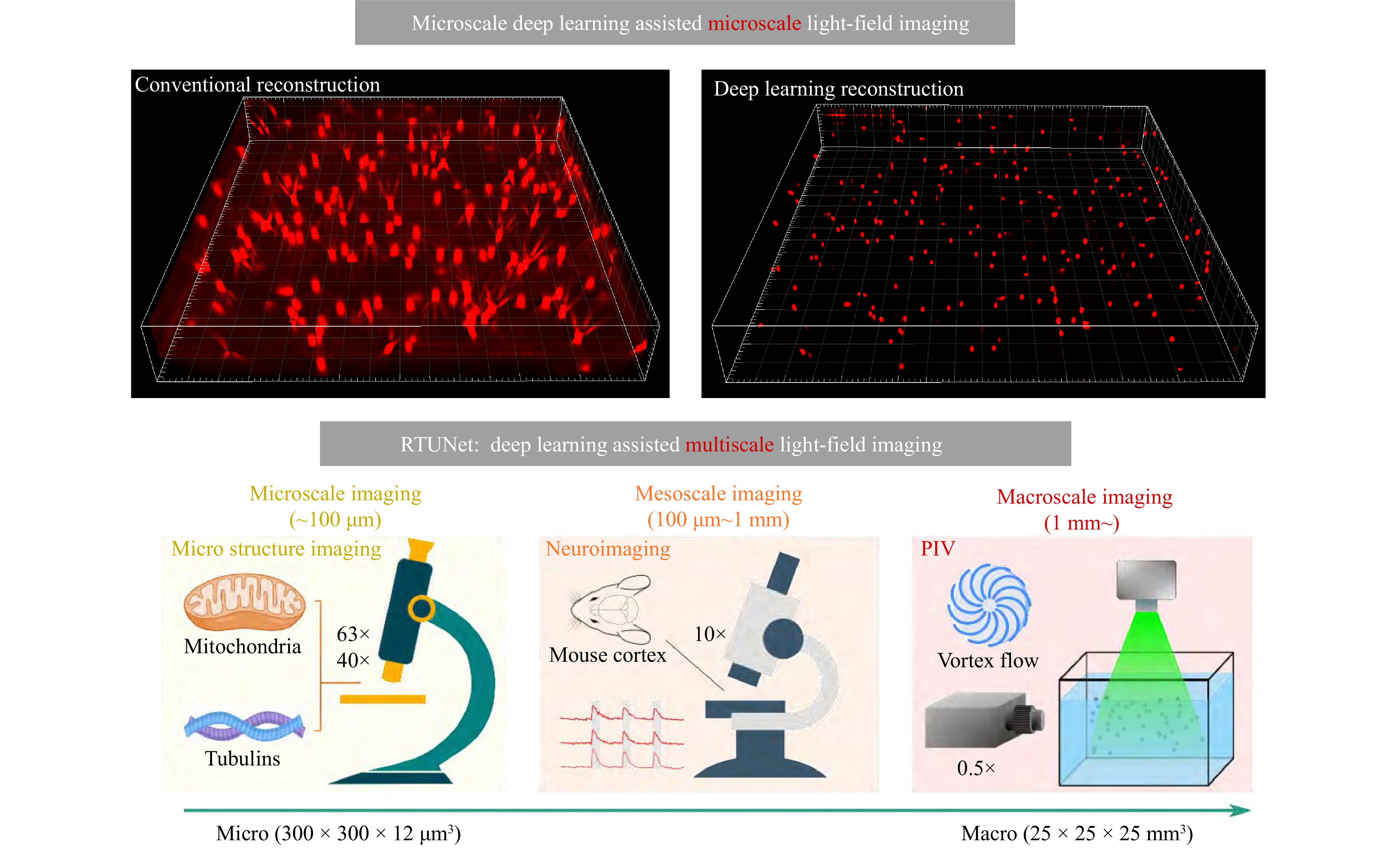
A real-time and universal network (RTU-Net) has been proposed for multiscale, real-time, high-resolution reconstruction of light-field images. The proposed RTU-Net can be applied to various application domains to gain insights into volumetric imaging from microscale to macroscale.
Published. 2025, 6(3)
: 402-403
doi: 10.37188/lam.2025.051
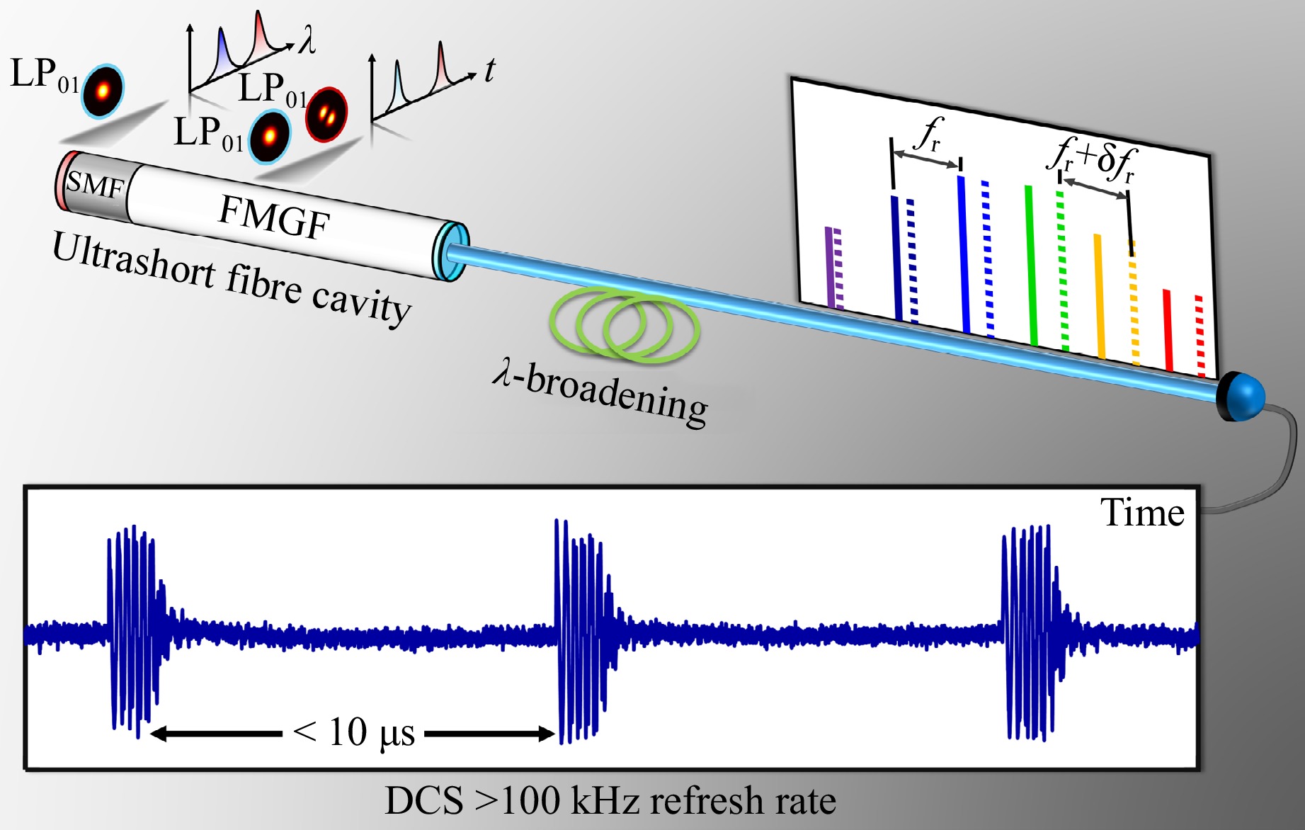
A single-cavity all-fibre laser operating at GHz rates is demonstrated as a promising approach for fast spectroscopy. Multimode-interference-based spectral filtering in the laser enables dual-wavelength mode-locked pulse generation (thus, dual-comb emission) with a 148 kHz repetition rate difference. The GHz dual-comb laser exhibits excellent stability and can be used for outdoor measurements.
Published. 2025, 6(3)
: 404-405
doi: 10.37188/lam.2025.036
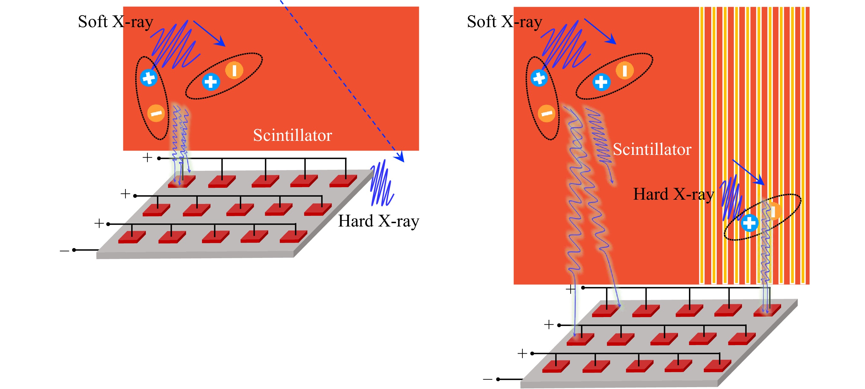
X-ray-responsive materials are often expensive and limited because of the monopolistic and complex high-temperature crystallisation technology required. Solution-processed material innovation offers a low-cost and vast design space for a new generation of X-ray detectors aimed at for high X-ray imaging performance.
Published. 2025, 6(3)
: 406-409
doi: 10.37188/lam.2025.054
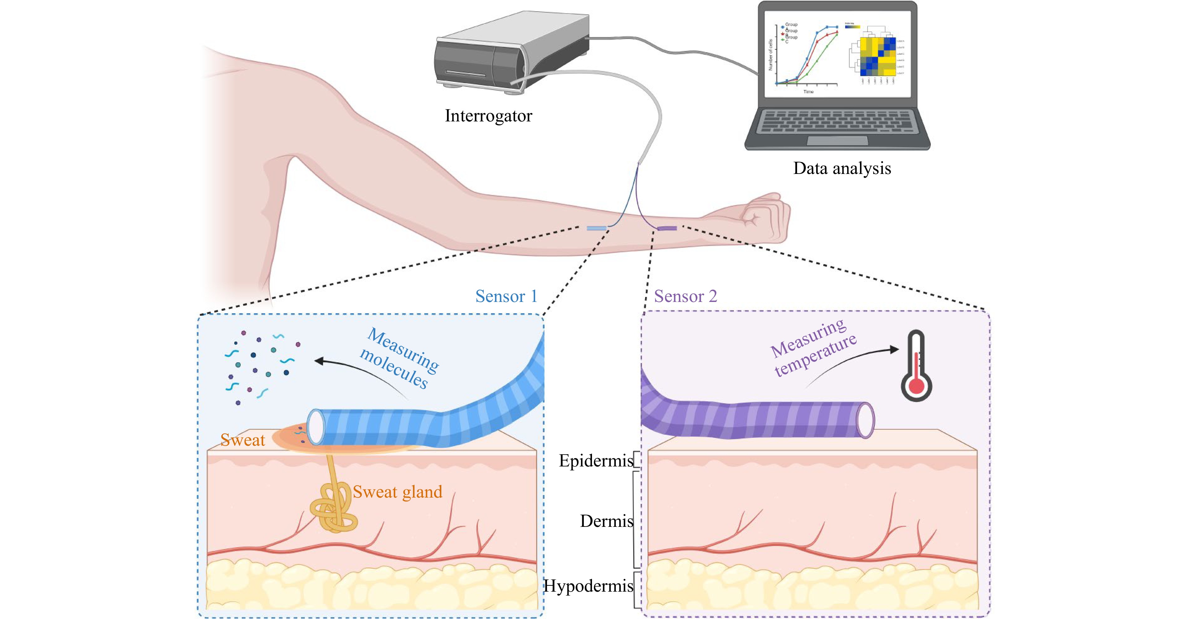
The real-time measurements of surface physiological parameters, such as body temperature, cardiorespiratory rates, and sweat, is of increasing importance in healthcare. Optical fibres can offer an effective solution for contact sensing, as they enable multi-parameter and multi-point sensing while maintaining a compact form factor. Recent advances using chalcogenide and other specialty fibres represent a substantial step towards all-fibre wearable devices.
Published. 2025, 6(3)
: 410-412
doi: 10.37188/lam.2025.052
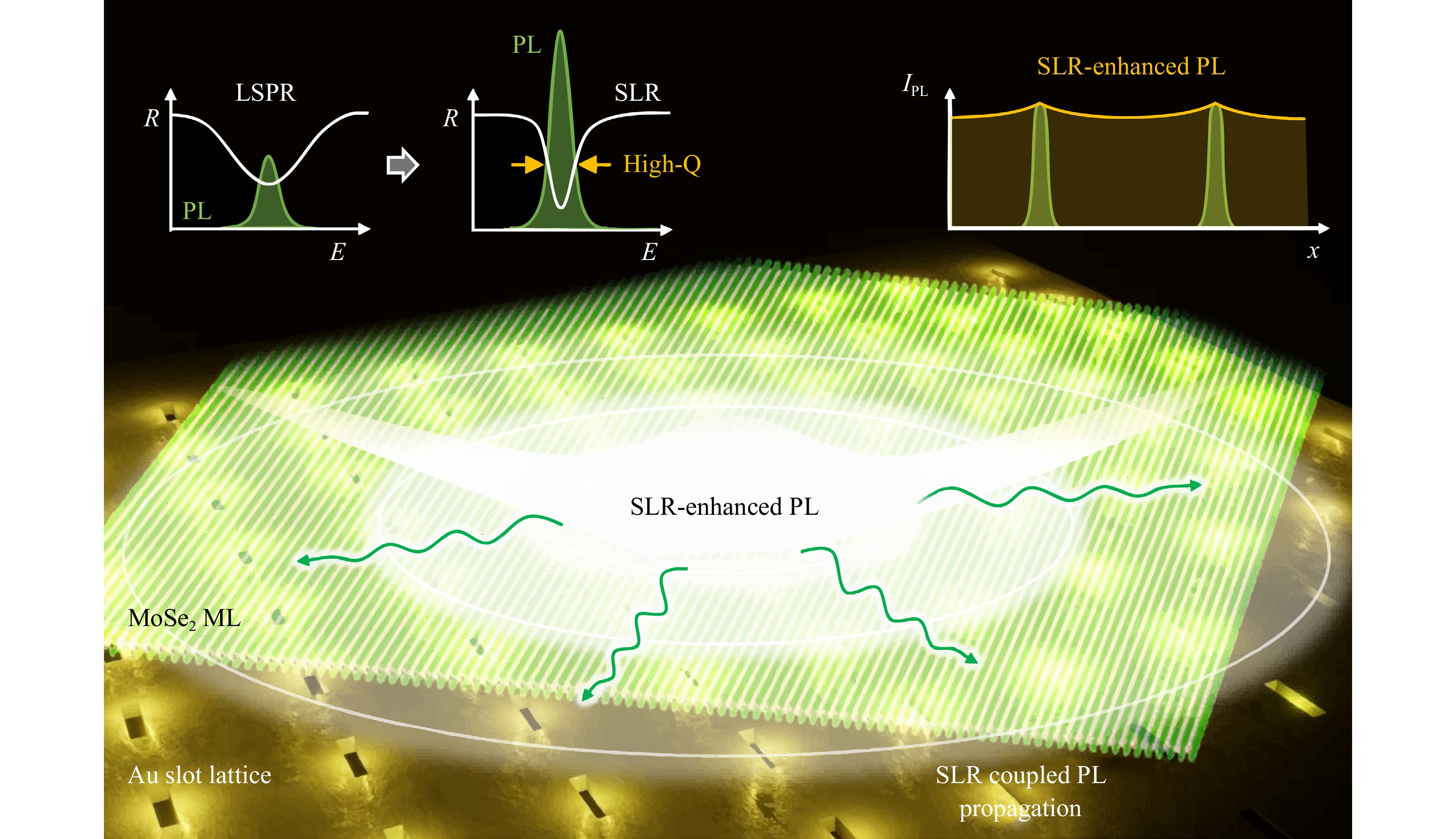
Recent progress in harnessing surface lattice resonance within a van der Waals material–Au slot lattice hybrid platform has enabled a 32-fold enhancement in two-dimensional photoluminescence over an 800 μm2-area, which is promising for realising scalable atomically thin light-emitting devices.
Published. 2025, 6(3)
: 413-415
doi: 10.37188/lam.2025.053
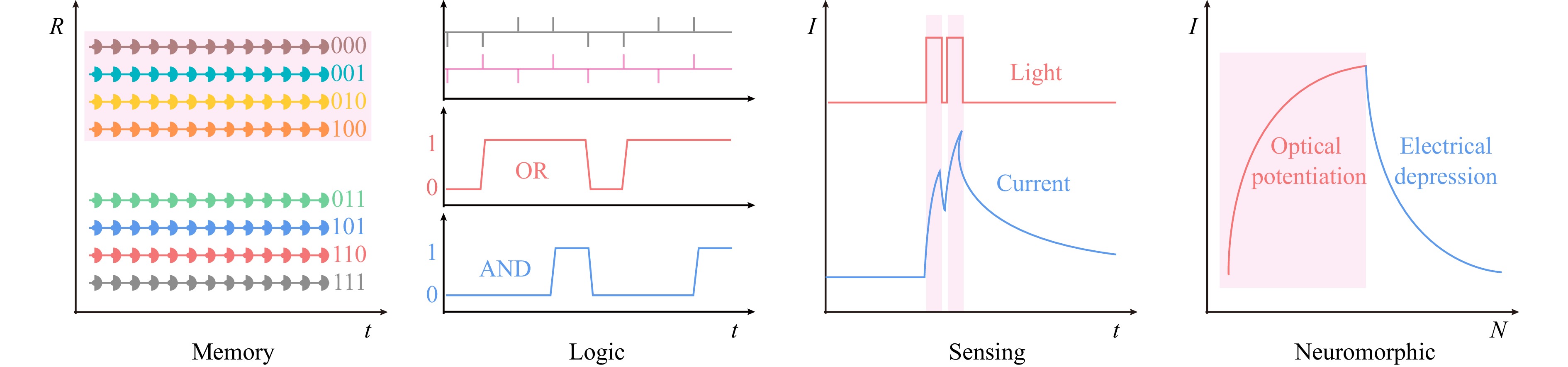
An amorphous Ga2O3 versatile memristive device has been fabricated to realise four-in-one functionality, merging multibit memory, logic operation, light detection, and neuromorphic computation.
Published. 2025, 6(3)
: 416-427
doi: 10.37188/lam.2025.062
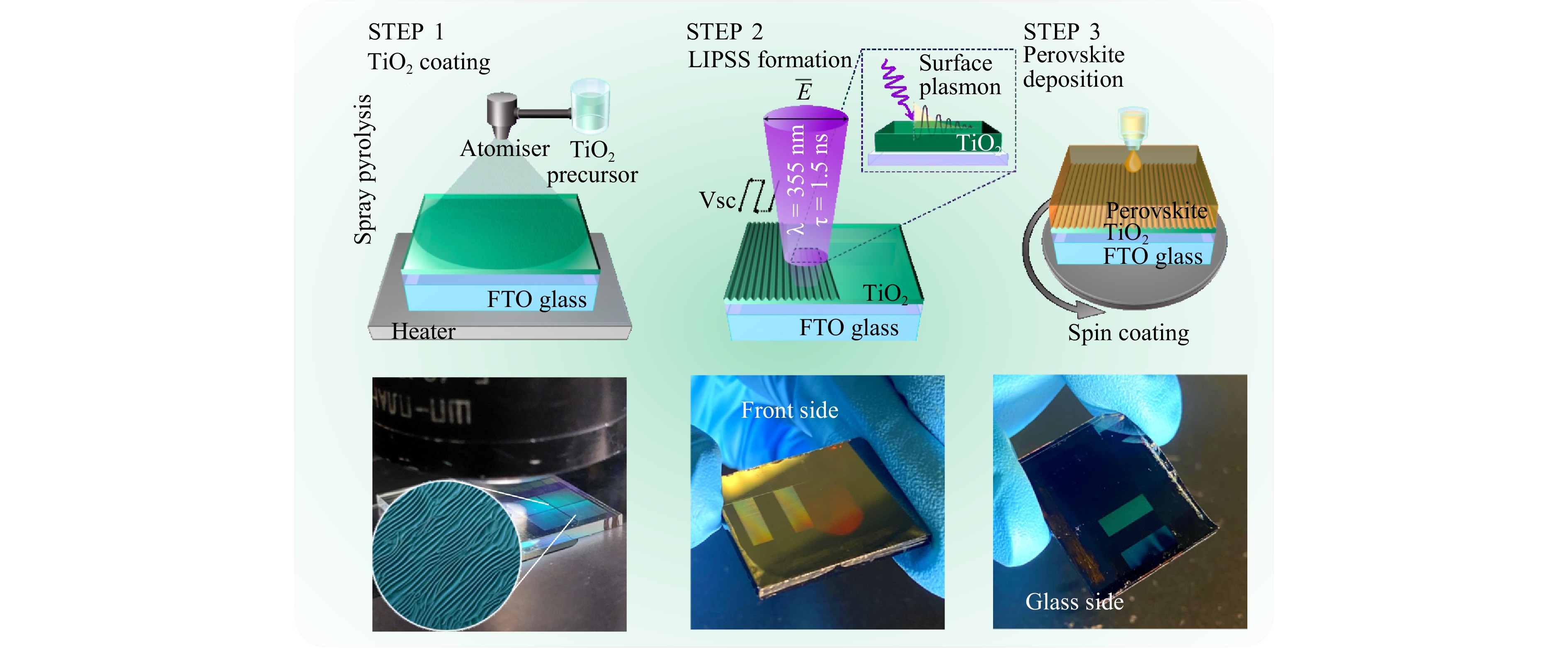
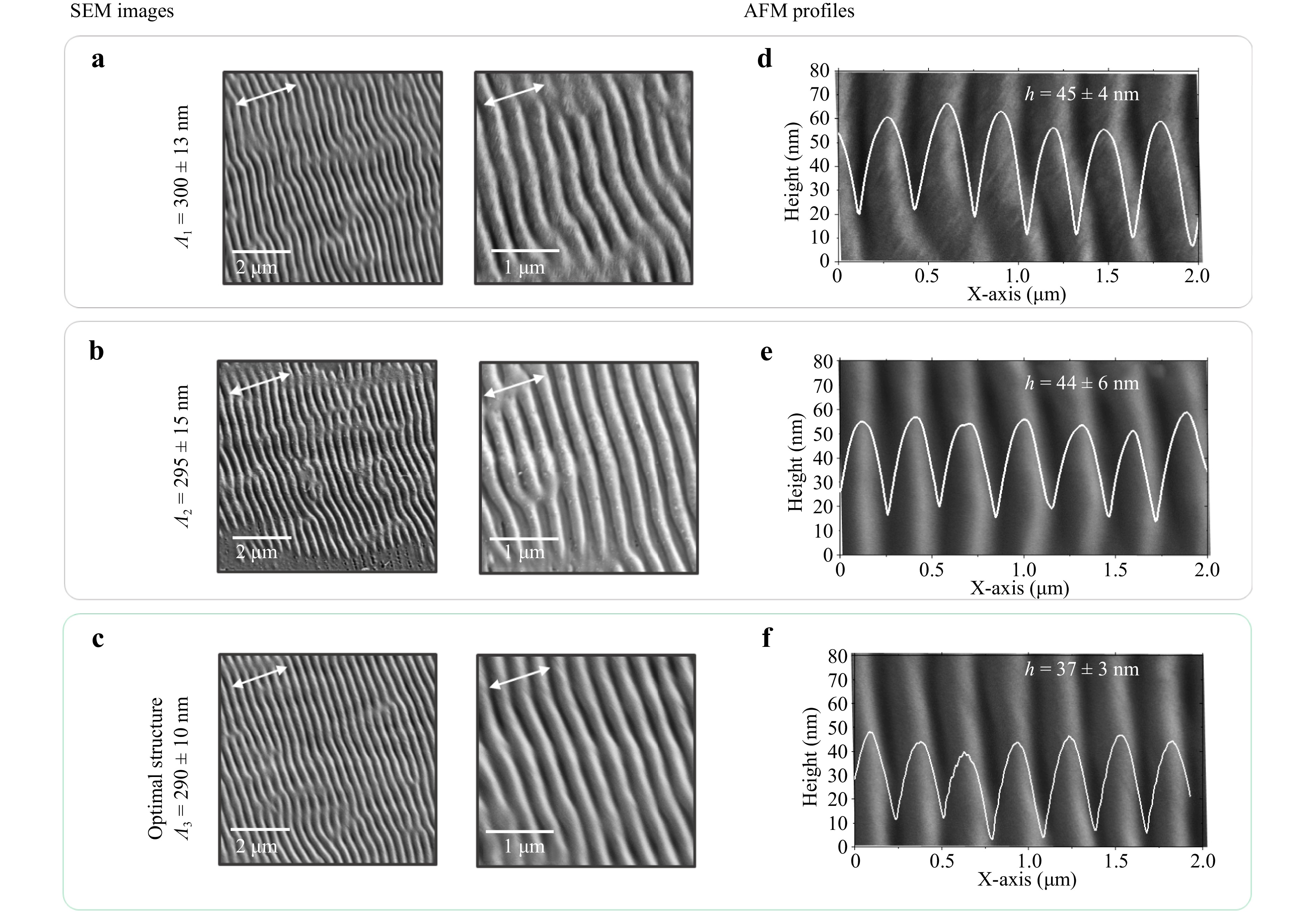
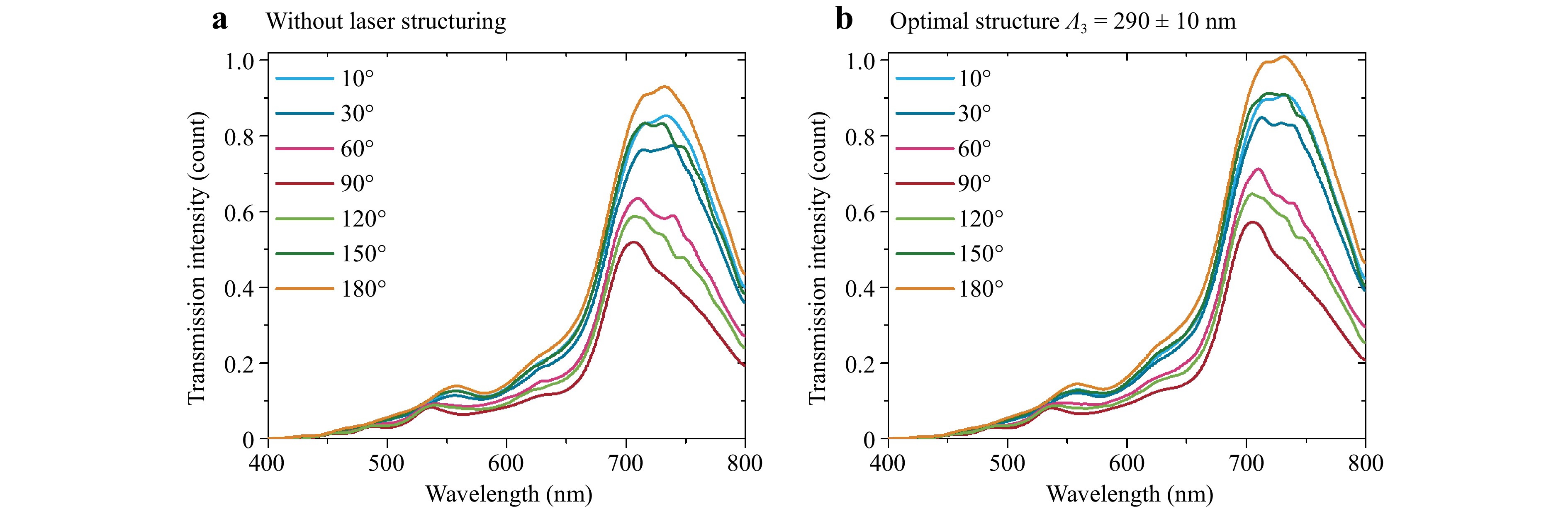
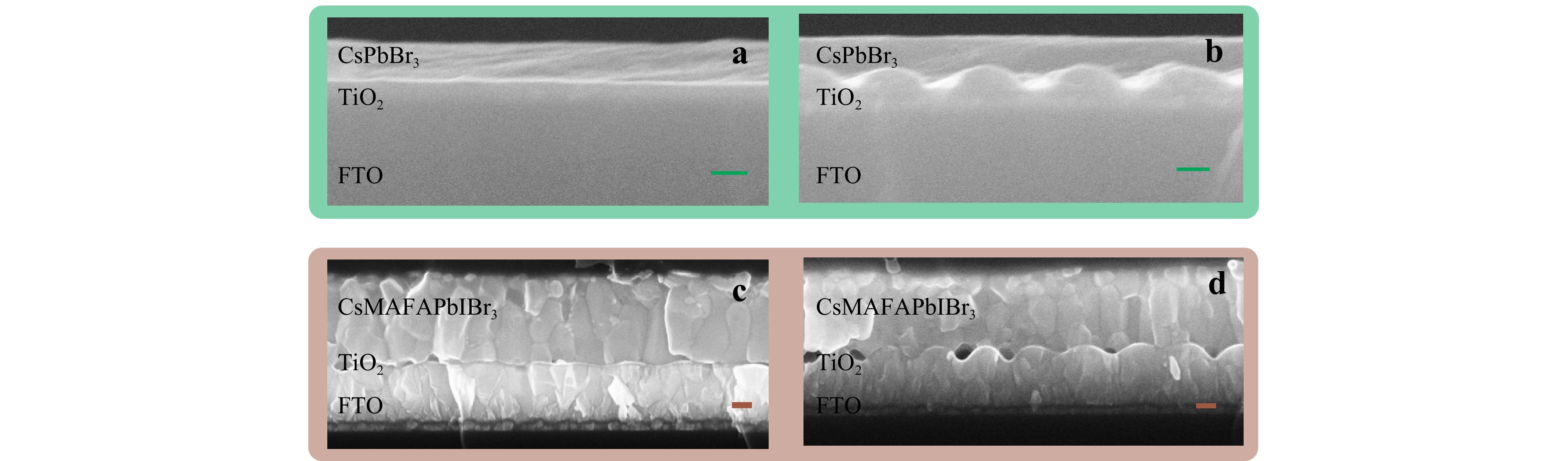
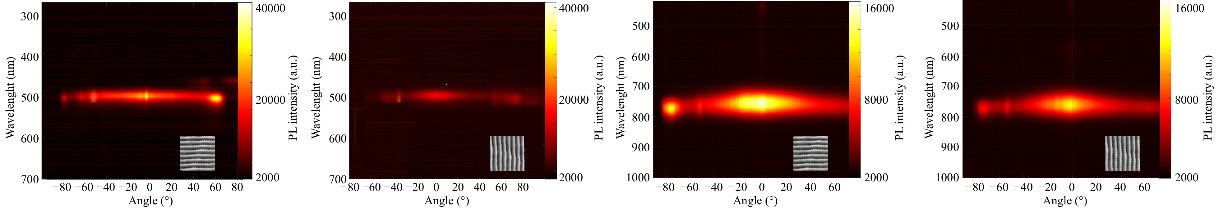
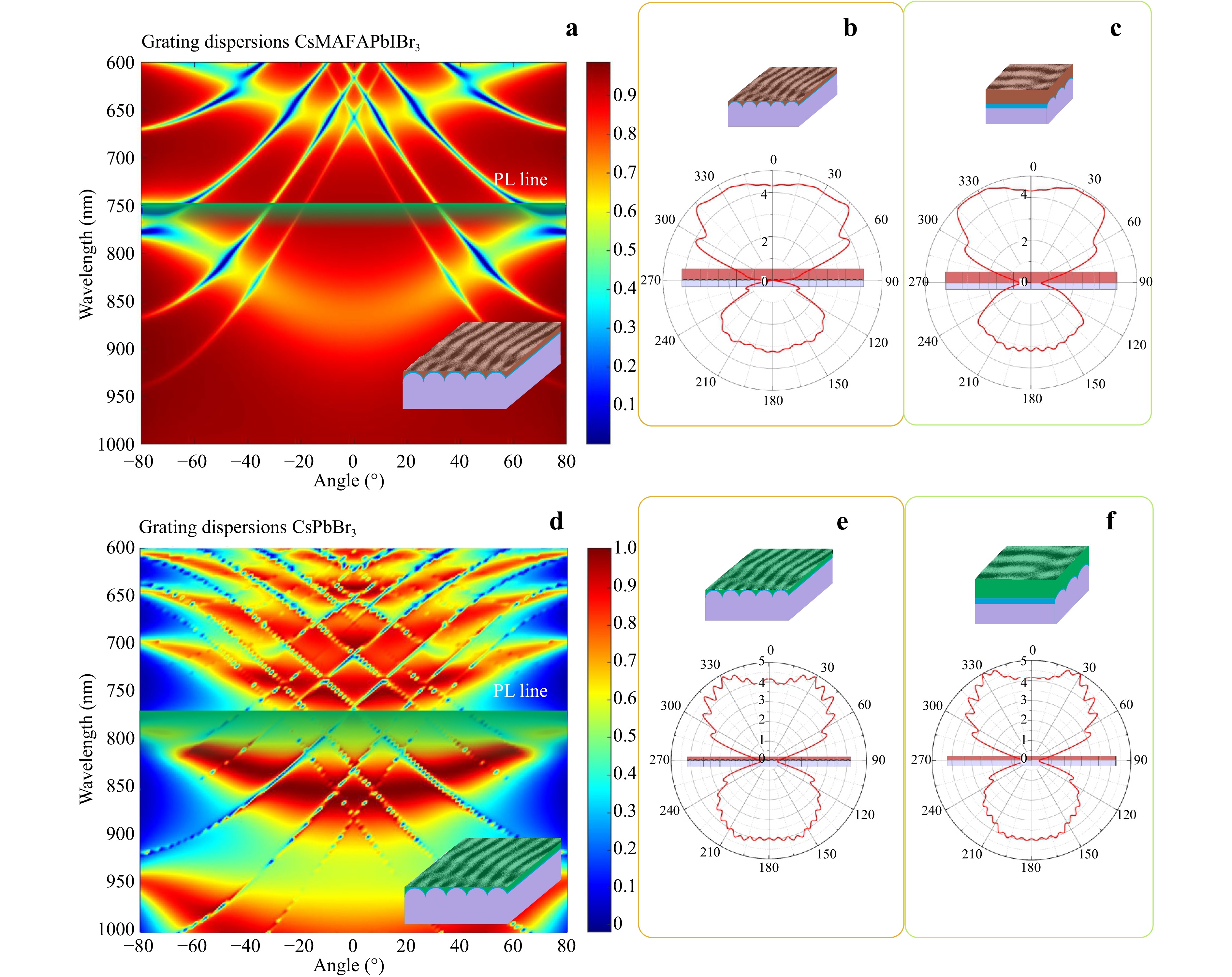
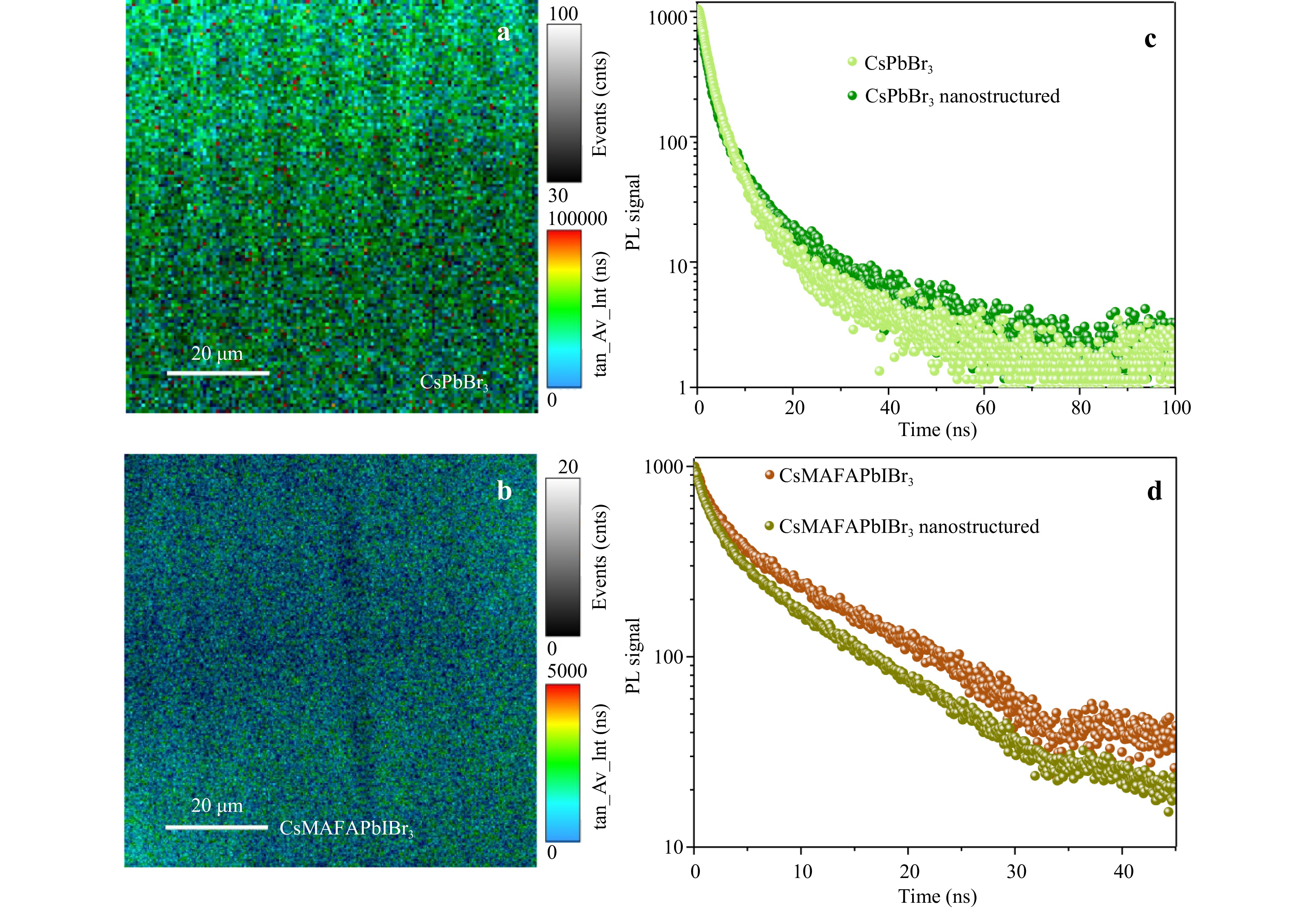
Perovskite nanostructured films are essential to create advanced optoelectronic and photovoltaic devices because of the additional degrees of freedom of manipulation by light reflection and structural colouration, as well as by light trapping and localisation, resulting in control of intensity or polarisation of luminescence. In this paper, we report structural colouration and photoluminescence anisotropy in perovskite films deposited on a substrate with laser-induced periodic surface structures (LIPSSs) on a thin TiO2 layer. The LIPSS TiO2 layer improves charge extraction from the perovskite films, confirmed by a time-resolved photoluminescence analysis. The developed method of substrate nanostructuring does not damage the perovskite films, in contrast to direct laser ablation, imprinting by a mould, mechanical scratching with a cantilever, or plasma-chemical etching. Moreover, the LIPSS formation is appropriate for upscaling owing to the high speed of LIPSS writing (2.25 cm2min-1) and uniform surface nanostructuring.
Published. 2025, 6(3)
: 428-435
doi: 10.37188/lam.2025.043
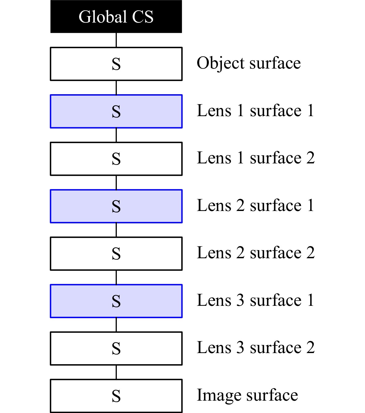
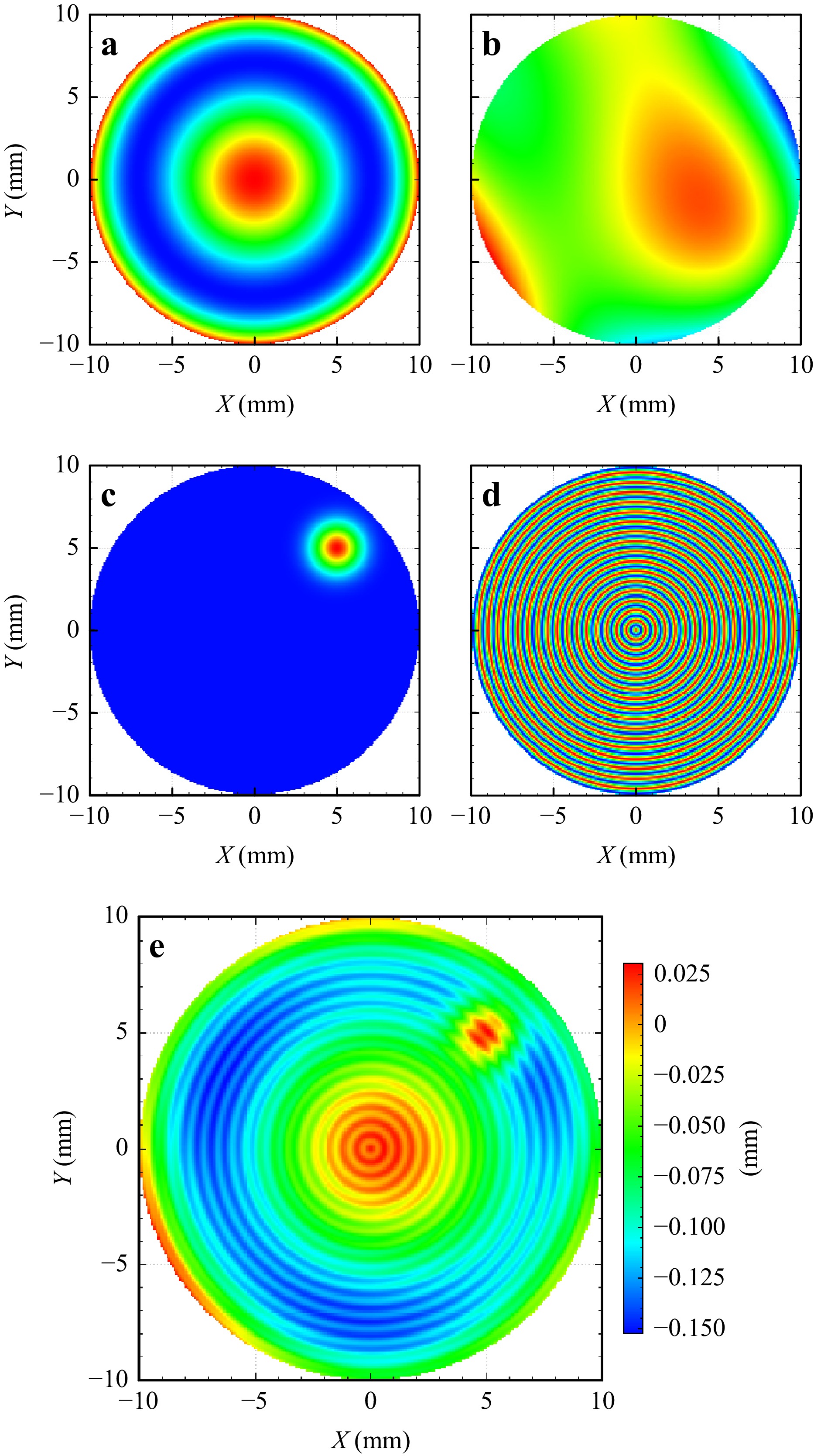
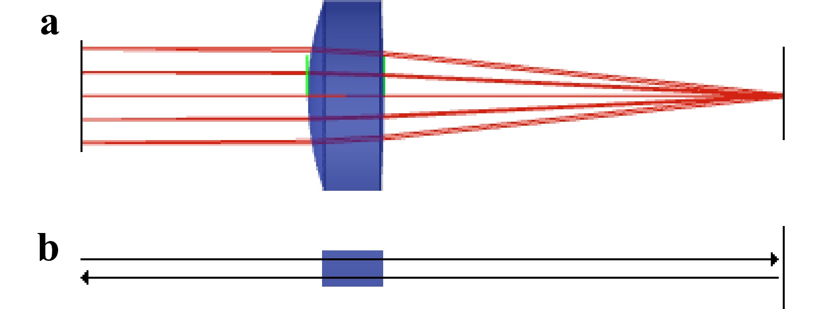
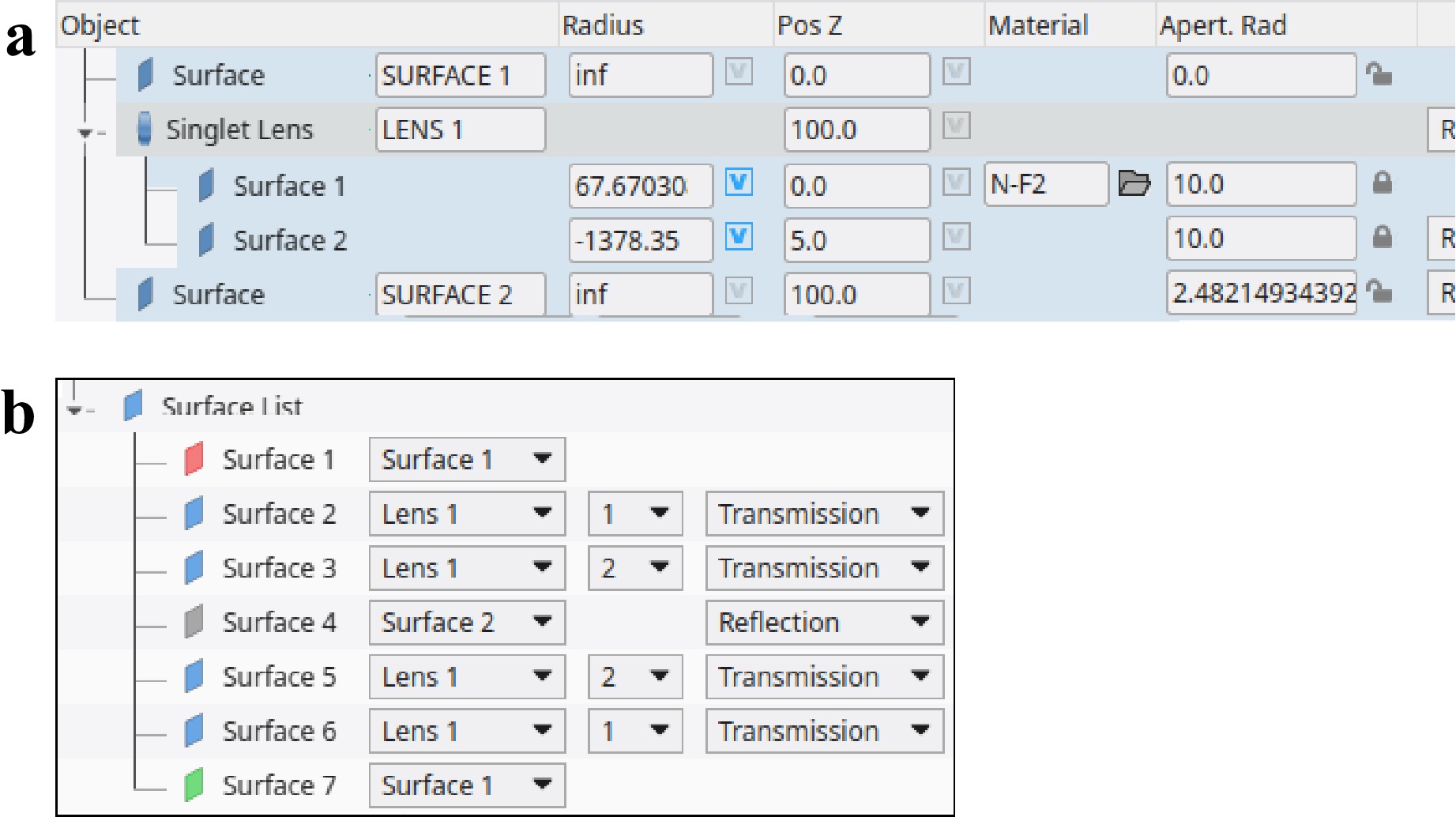
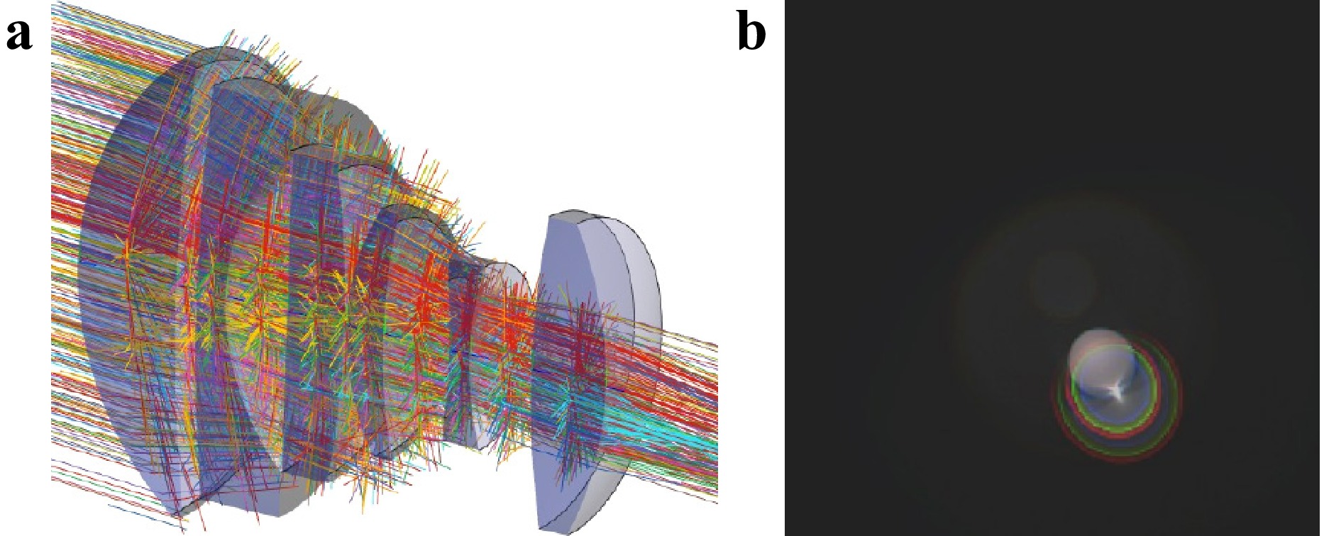
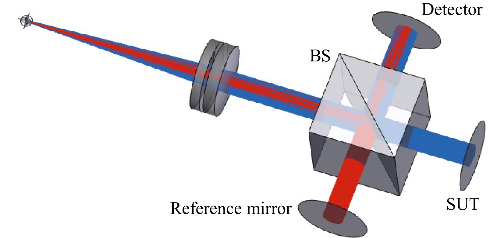
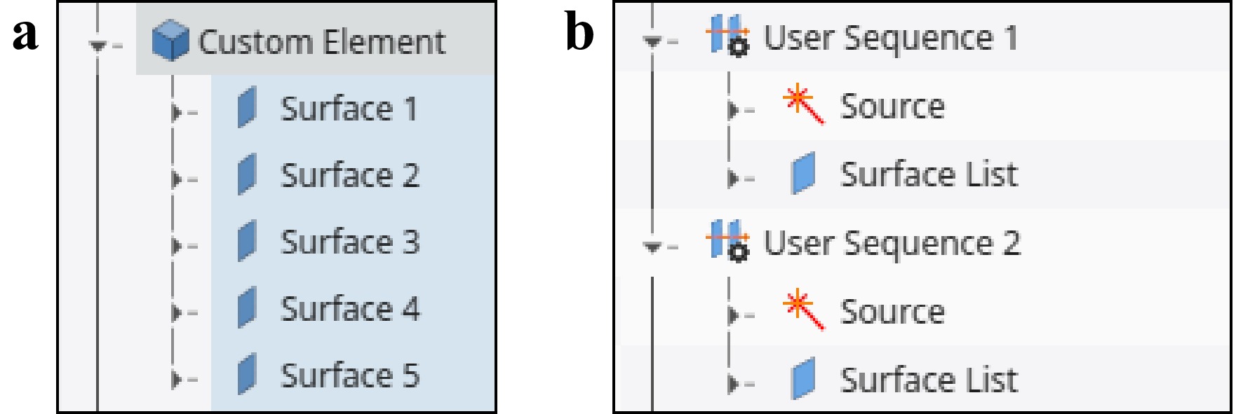
In the area of computer-aided optical design most software packages rely on a surface list based data structure. For classical on-axis lenses — such as camera lenses — the list-based data structure is a suitable way for managing lens data. However, for modern high-end optical systems such as off-axis free-form designs, multi-path systems or for accurate tolerance analysis of complex opto-mechanical systems, the list-based approach often reaches its limits. In this paper we present a new tree-like data structure that is able to solve many of the problems that emerge from surface list based data structures.
Published. 2025, 6(3)
: 436-446
doi: 10.37188/lam.2025.057
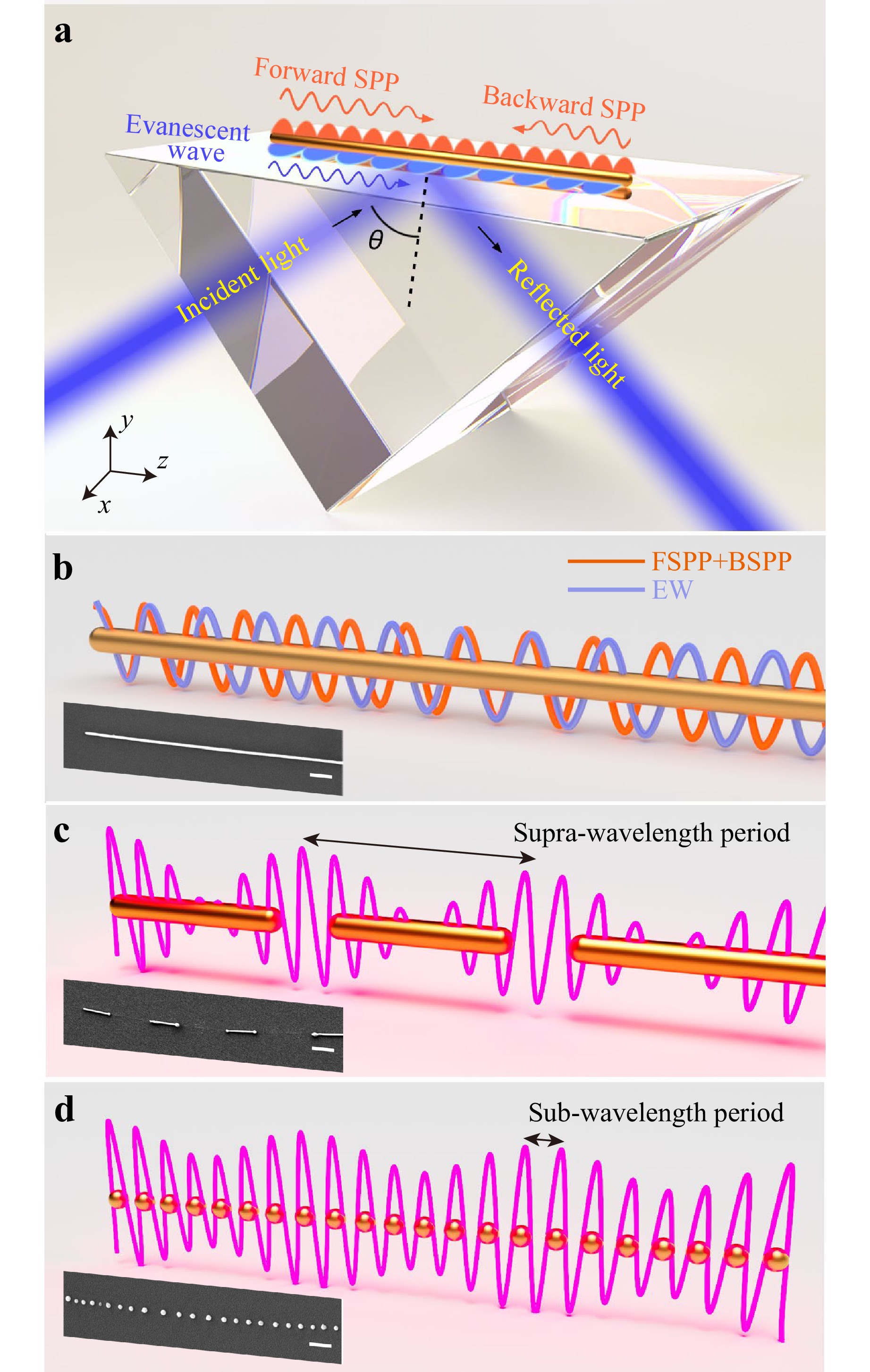
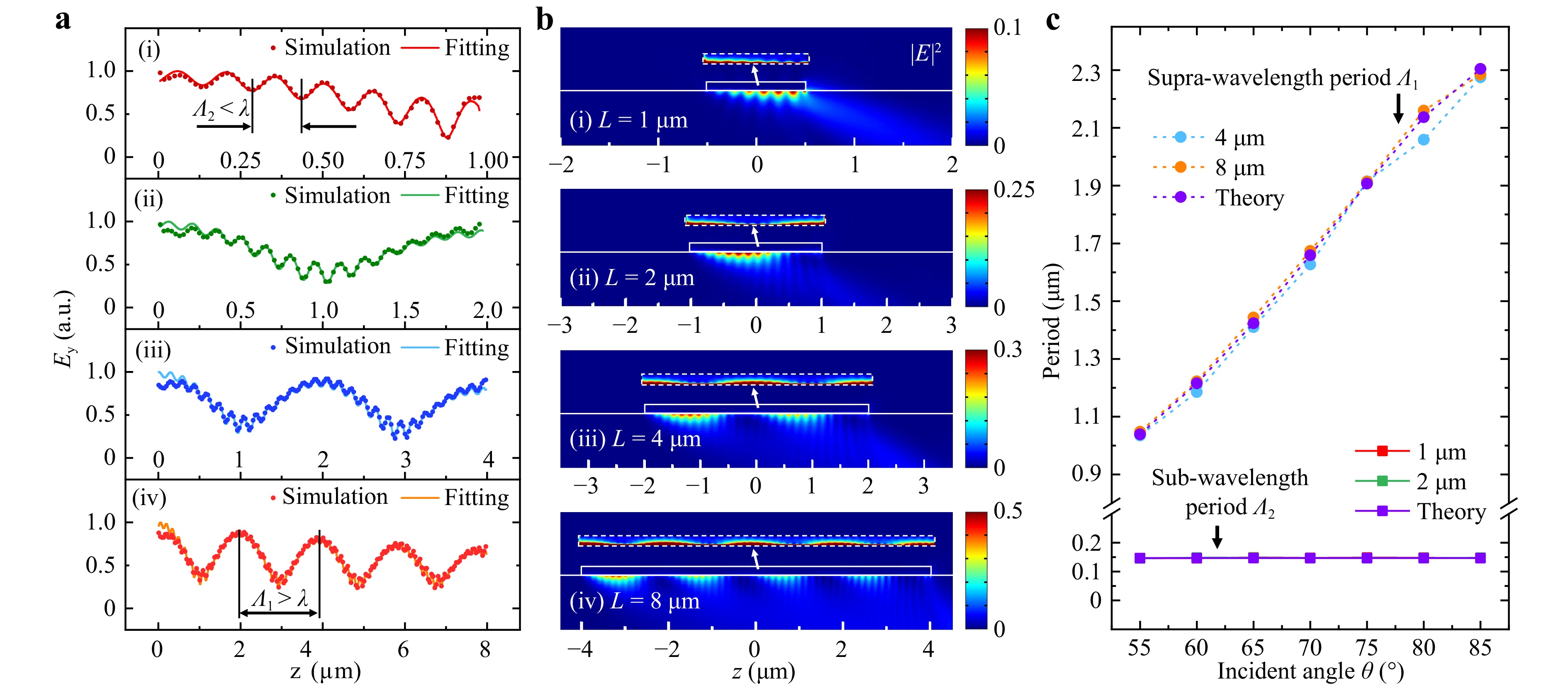
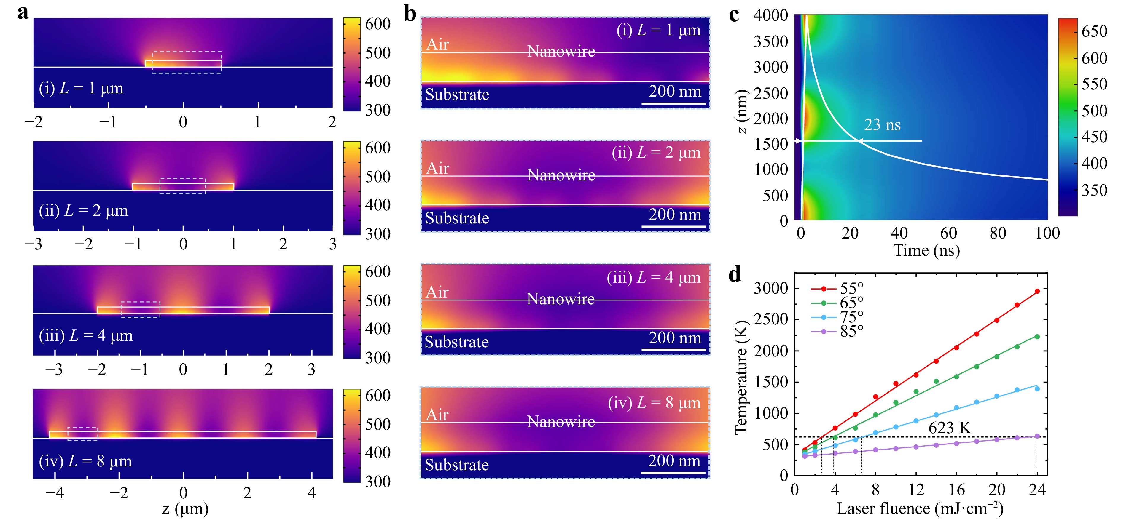
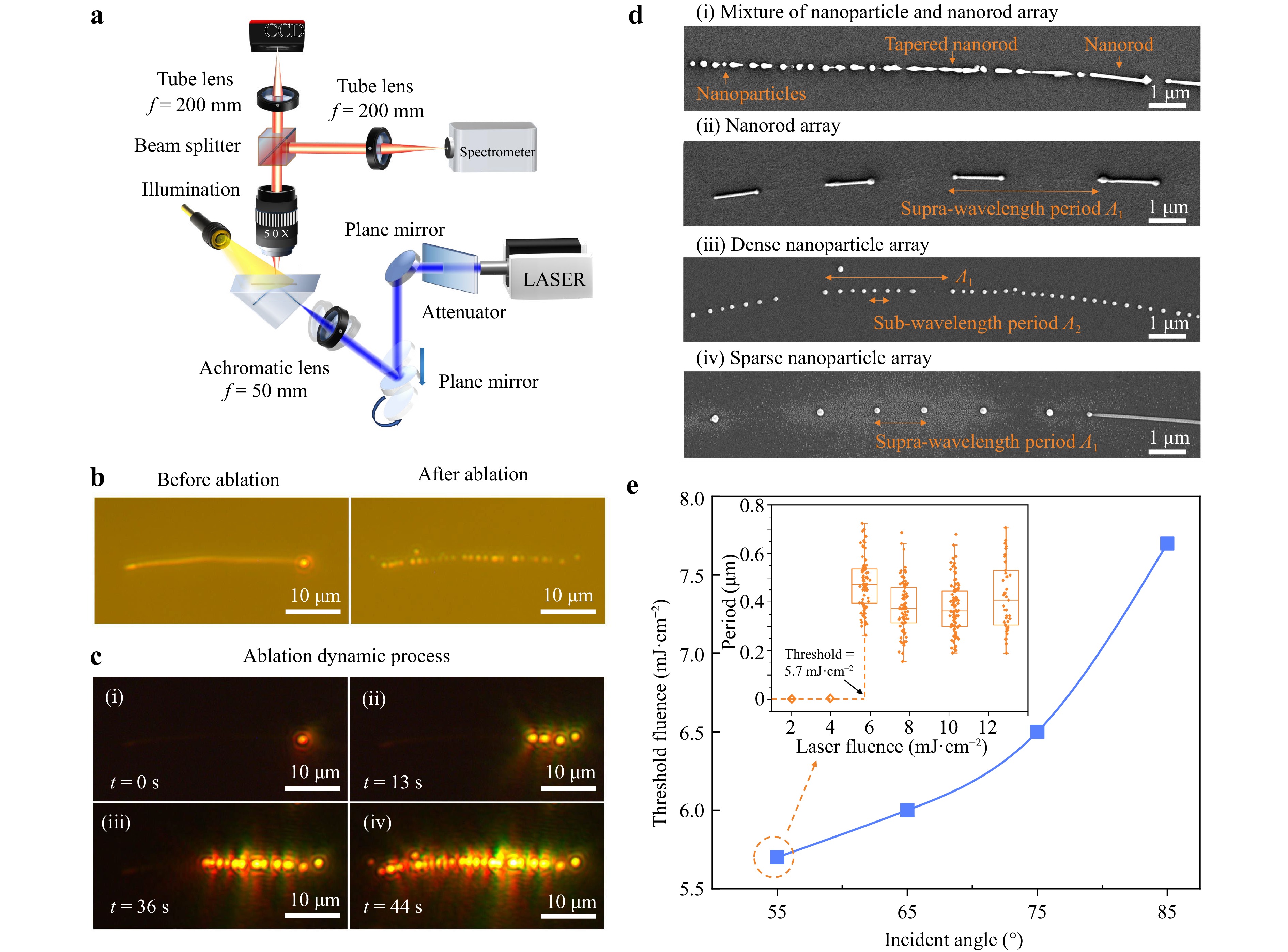
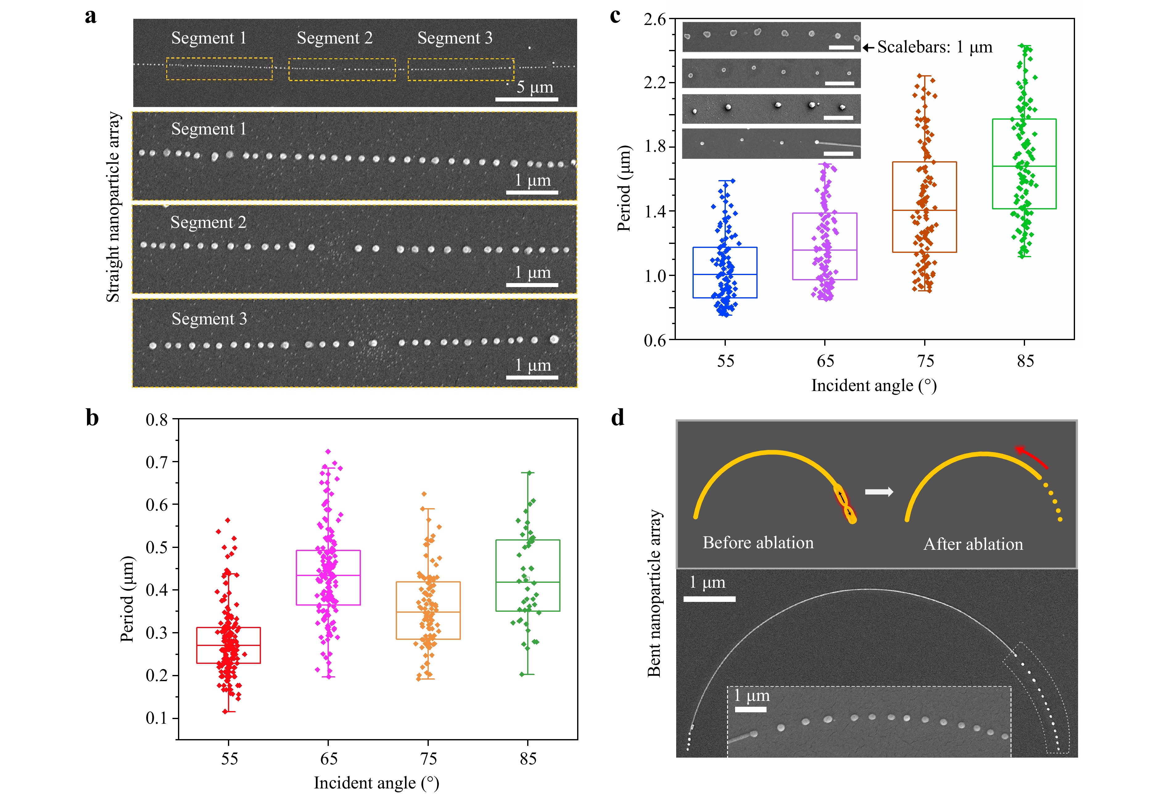
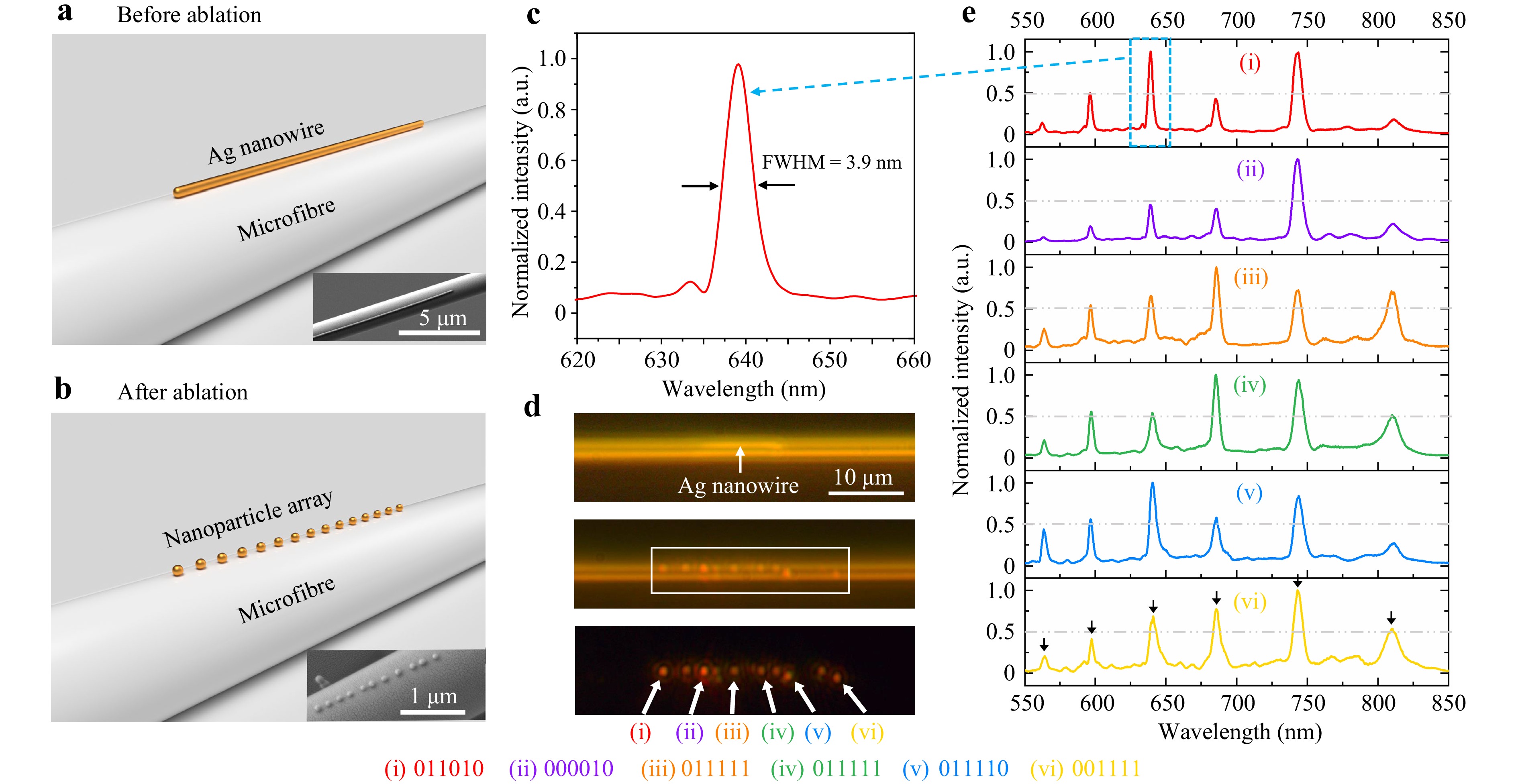
Assembling metal nanoparticles into a well-defined array and constructing strongly coupled hybrid systems enable high-quality resonances with narrow linewidths, which offer new opportunities to circumvent the hurdle of plasmonic losses. Herein, we propose a light-driven approach for generating plasmonic arrays by leveraging the self-organized patterns of tightly confined surface plasmon polaritons in single metal nanowires, which exhibit optimized unit structures, tunable interparticle spacings with supra-wavelength or sub-wavelength periods beyond the diffraction limit, and flexible alignment directions. We theoretically and experimentally show the mechanism of generating field patterns via the interplay of a standing wave and optical beating, followed by the formation of periodic geometries under a spatially modulated temperature distribution. We also fabricate plasmonic arrays on microfibres with diameters down to ~1.4 μm and thereby construct a series of hybrid plasmonic–photonic resonators with narrow-band resonances (~3.9 nm linewidth) as well as a barcode system with high multiplexing capacity. Our results show the potential of simple, low-cost, and high-efficiency fabrication of plasmonic arrays and hybrids that may find applications in plasmonic array lasers, information encryption, and high-resolution distributed sensing.
Published. 2025, 6(3)
: 447-458
doi: 10.37188/lam.2025.039
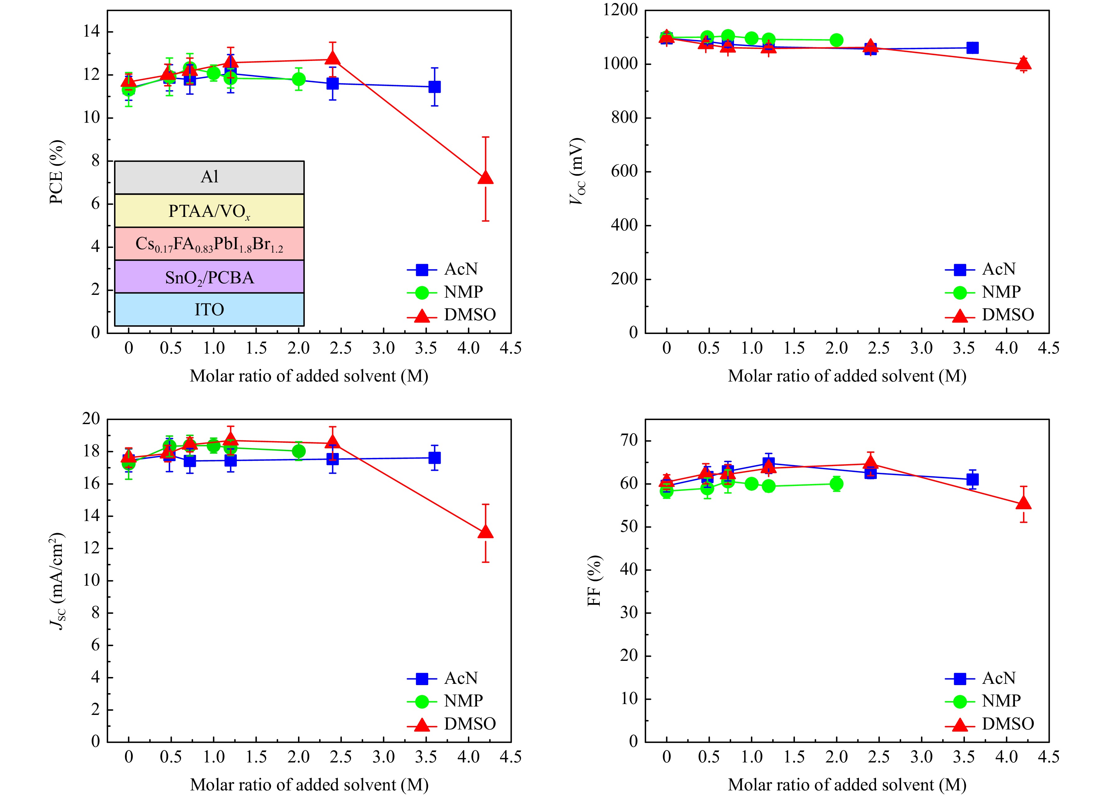
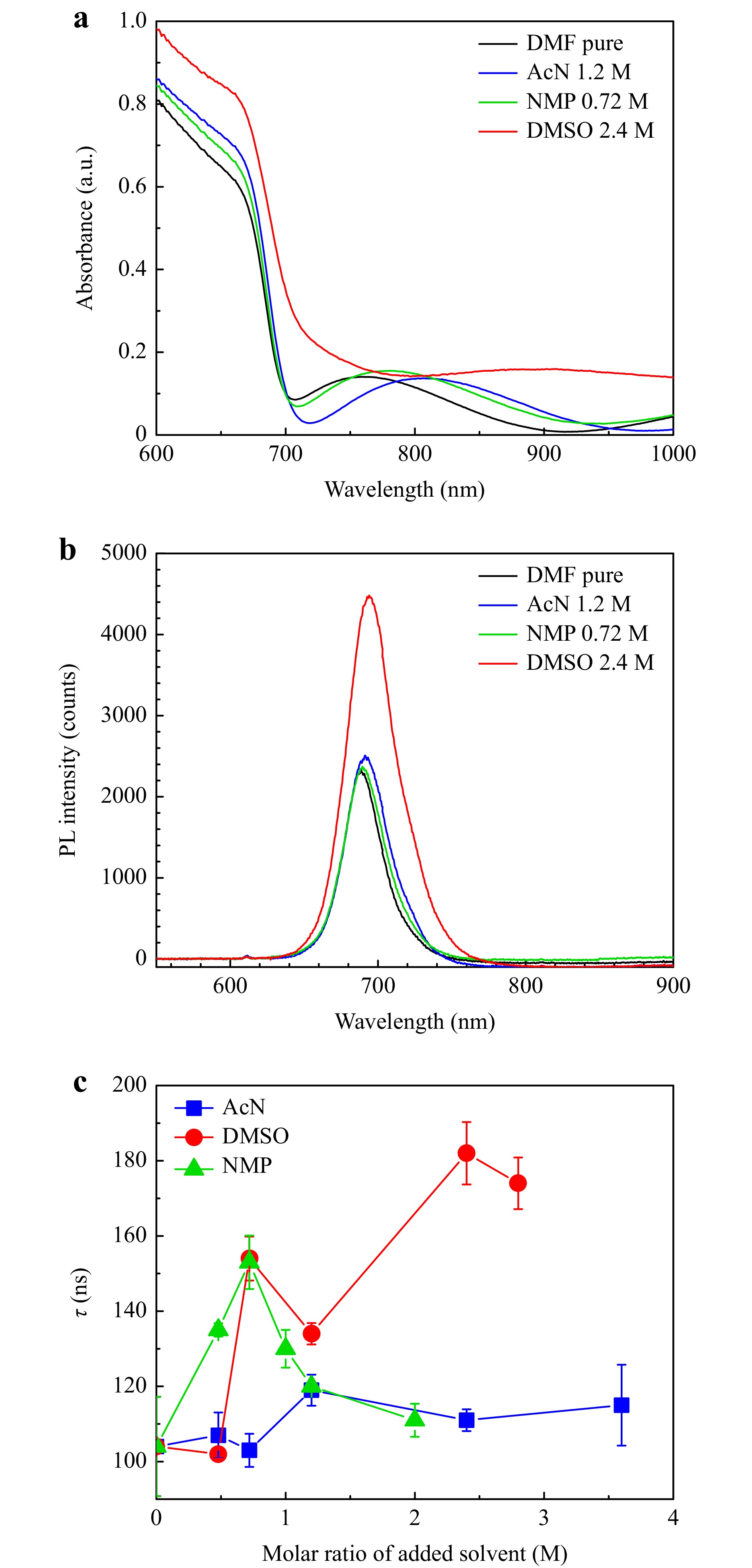
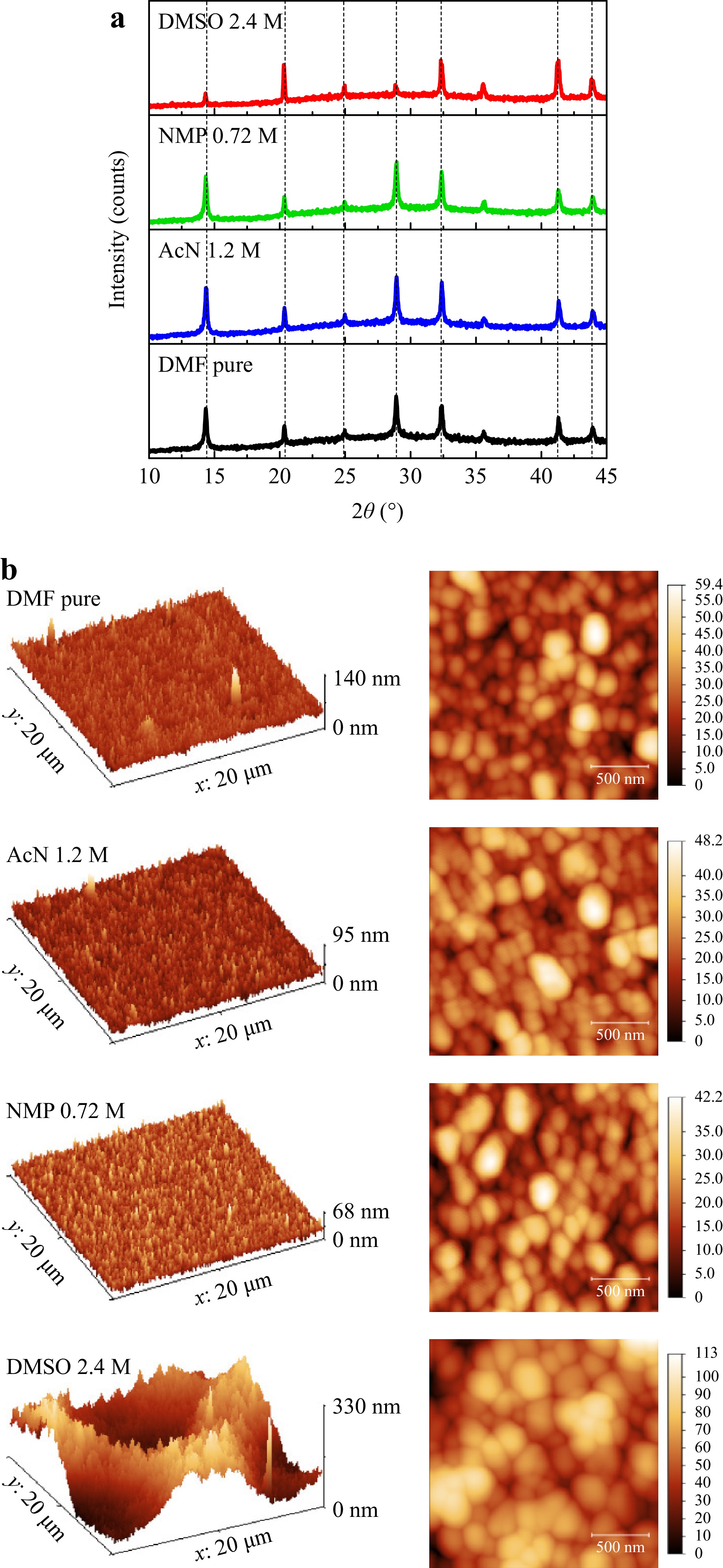
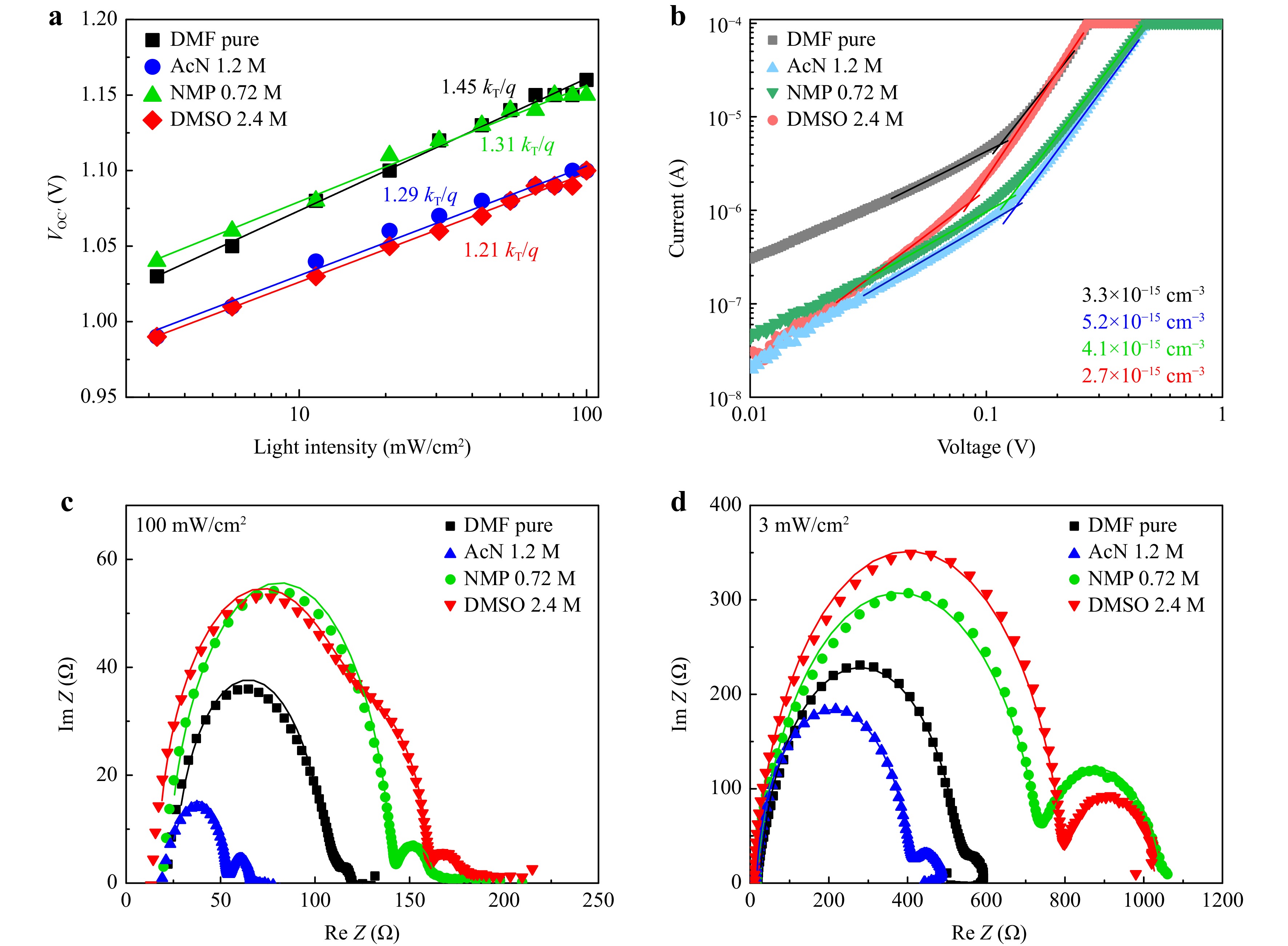
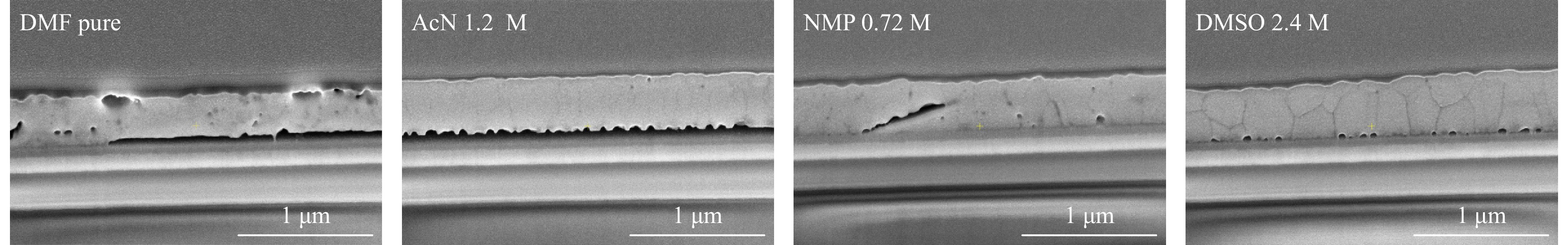
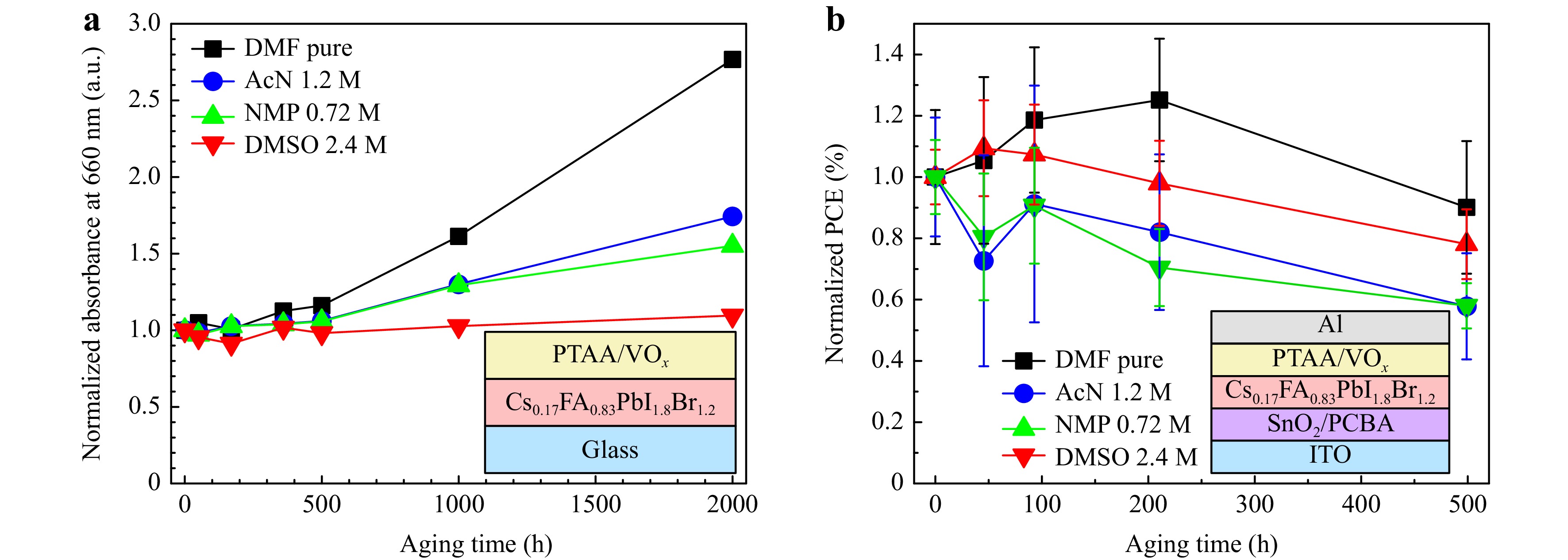
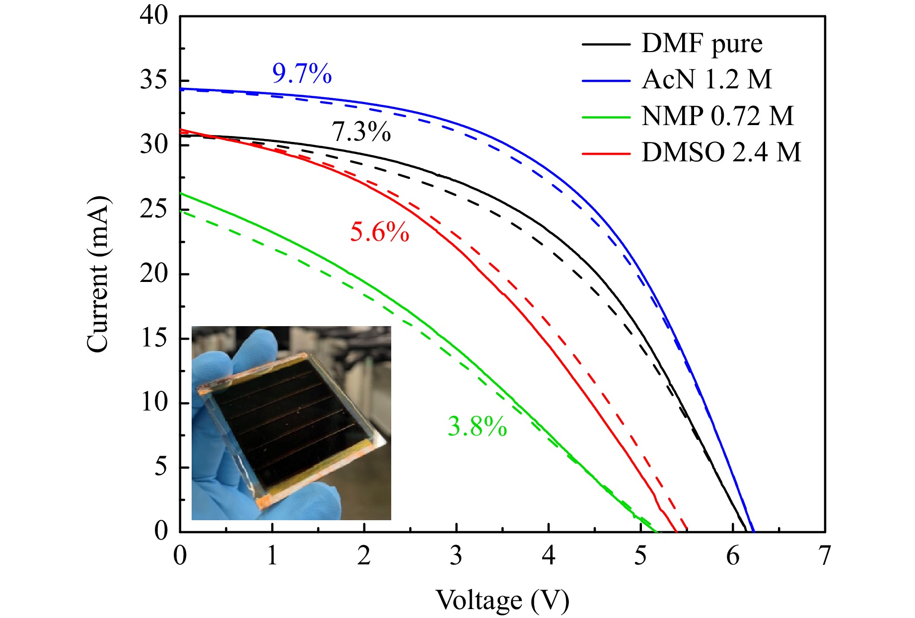
Perovskite photovoltaics upholds the most prominent position in the field of tandem technology development. In this aspect, the creation of perovskite material with suitable bandgap (≥ 1.65 eV) is necessary. And in order to achieve the best device characteristics, the high-quality film formation is crucial. To get a high-quality film, the solvent engineering approach stays at the forefront. However, although the solvent engineering was well discussed for such conventional material as MAPbI3, the field of wide bandgap perovskite materials is still lacking in this area. This paper presents the solvent engineering approach to improve the efficiency and stability of the conventional wide bandgap perovskite material Cs0.17FA0.83PbI1.8Br1.2. Here we utilize several solvents such as traditional N,N-dimethylformamide, dimethyl sulfoxide, N-methyl-2-pyrrolidone and acetonitrile. It was demonstrated that implication of any binary DMF-X solvent improves the solar cell efficiency compared to the pure DMF solution, but the ratio of the X solvent is unique for every X and the foundation for the X influence is also unique. The addition of 2.4 M of DMSO is considered the best to improve the stability and efficiency of laboratory devices, however implementation of AcN allowed to produce 25 cm2 mini-modules with the PCE reaching 10%.
Published. 2025, 6(3)
: 459-473
doi: 10.37188/lam.2025.033
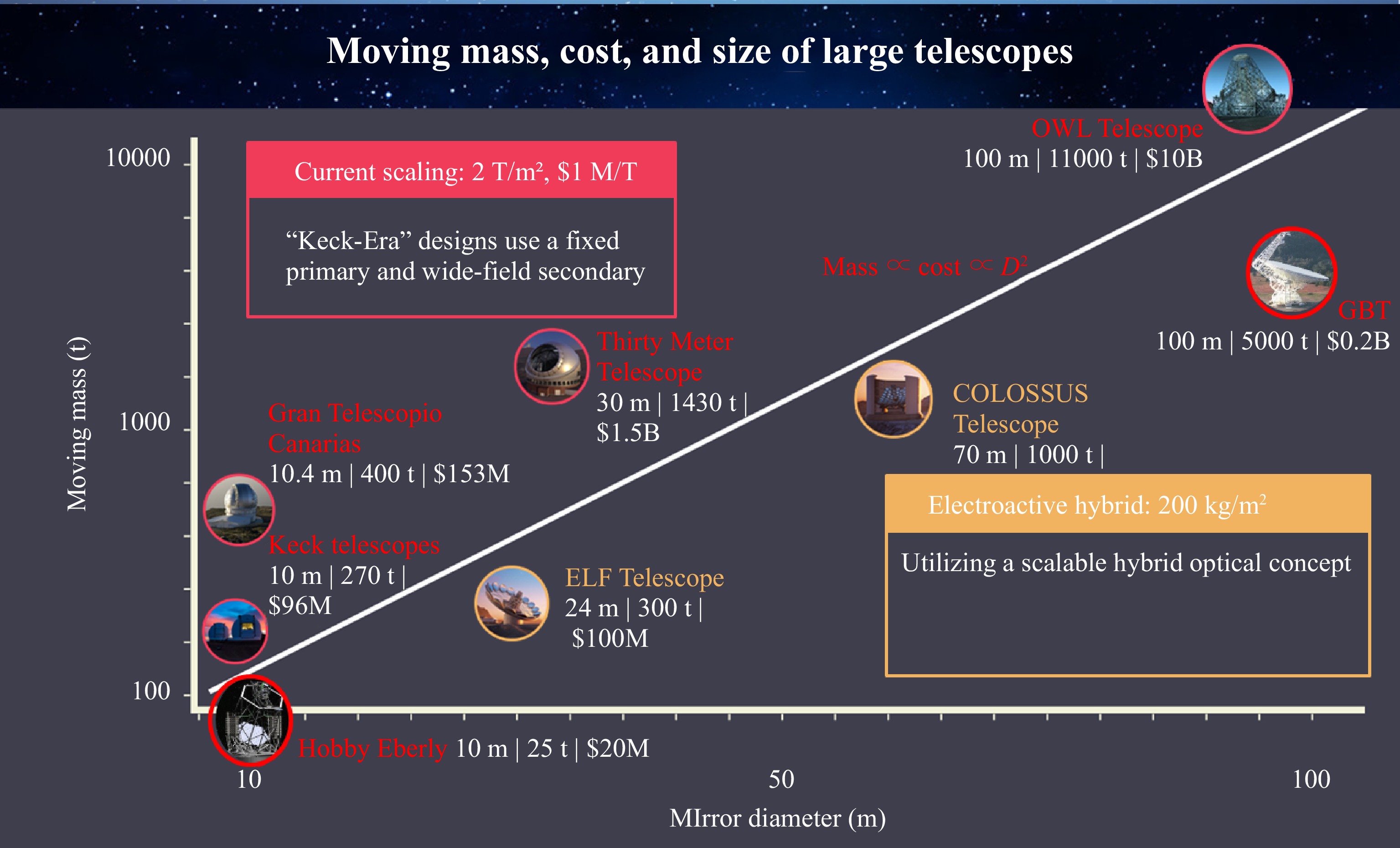
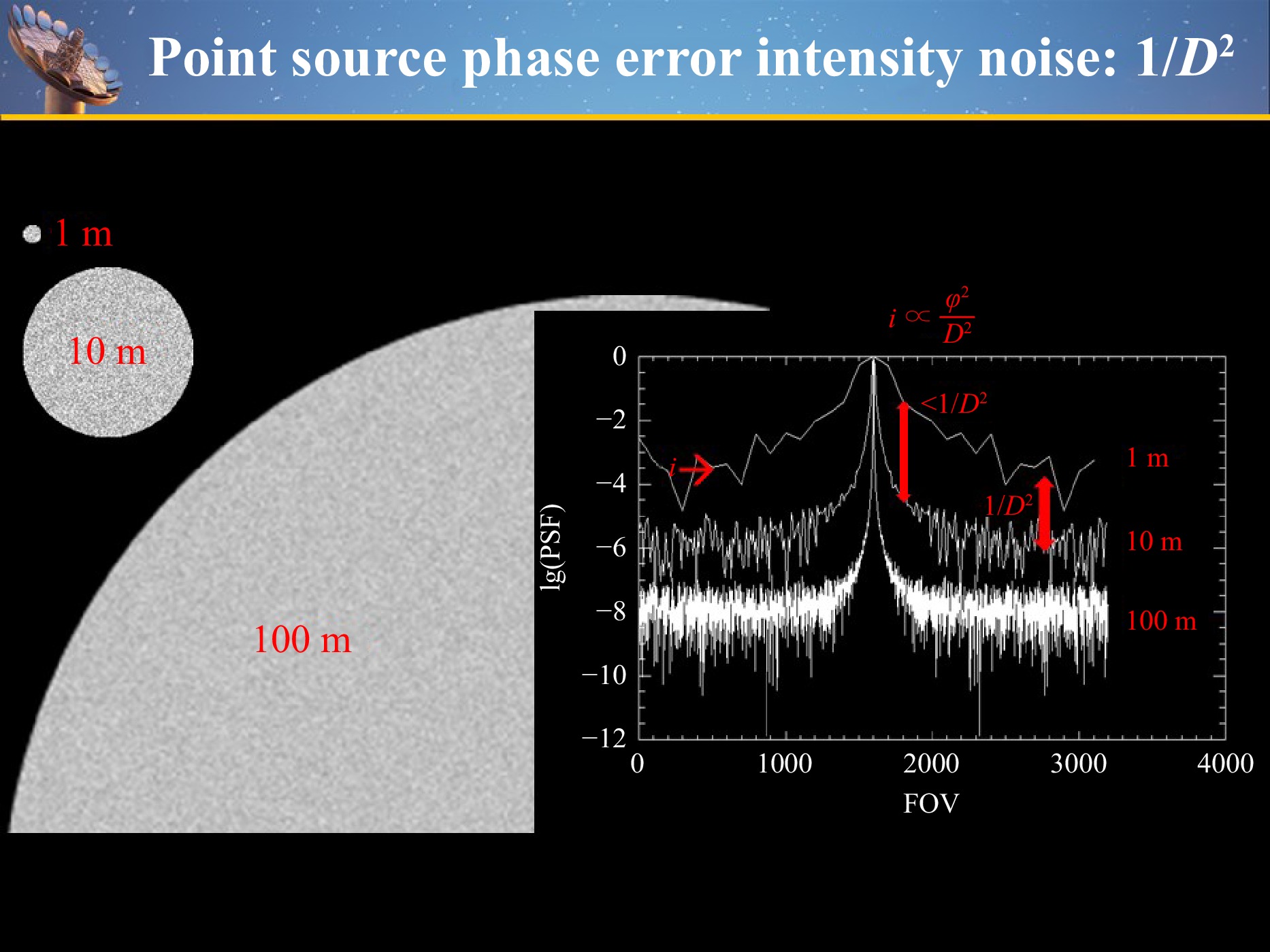
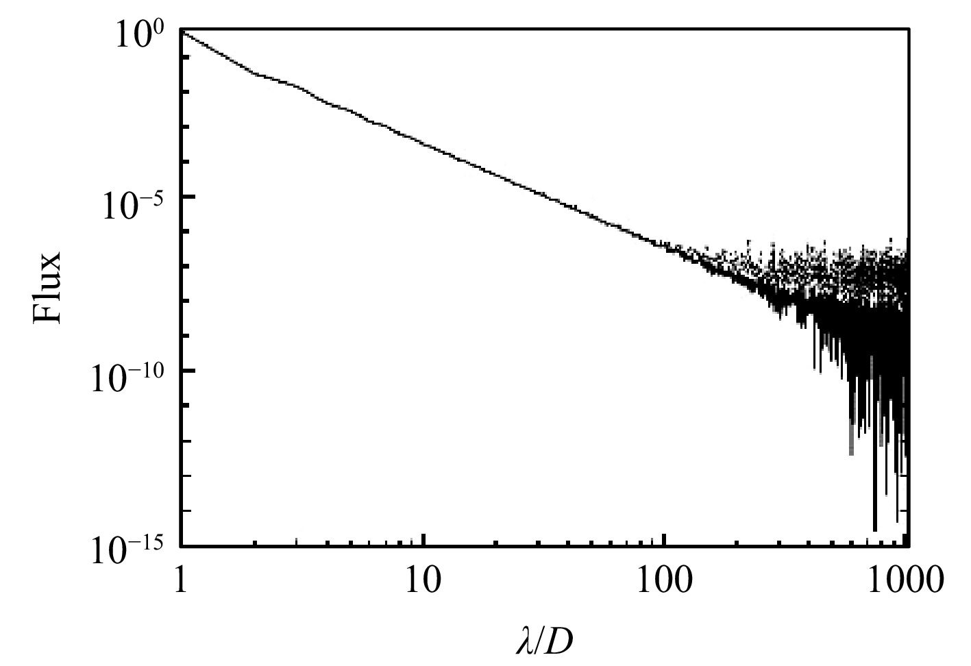
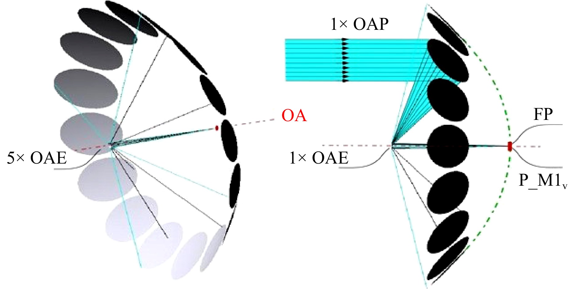
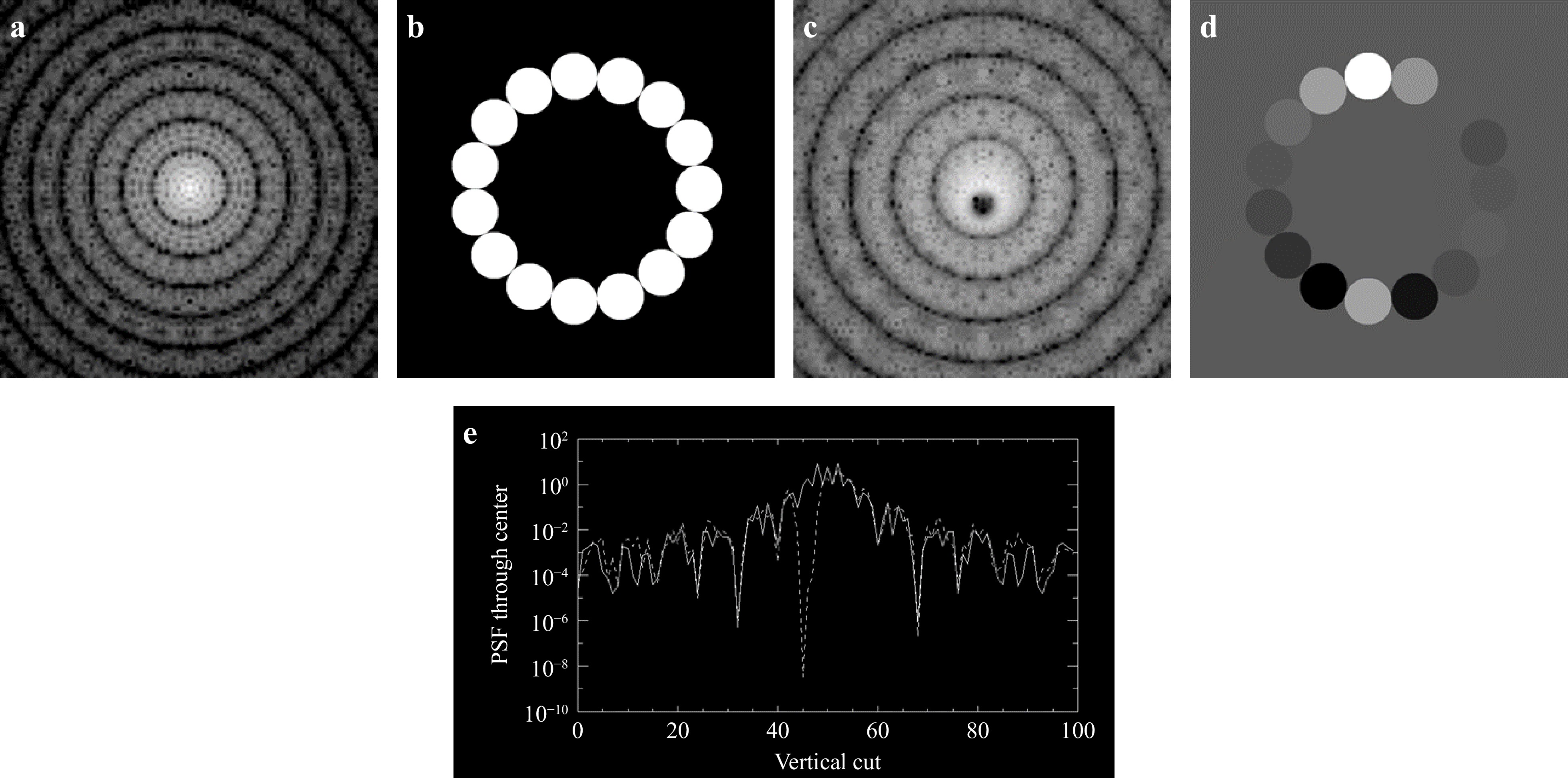
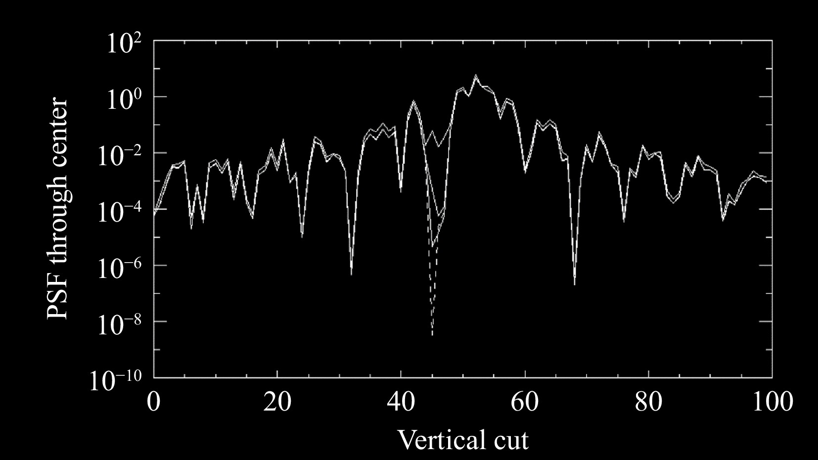
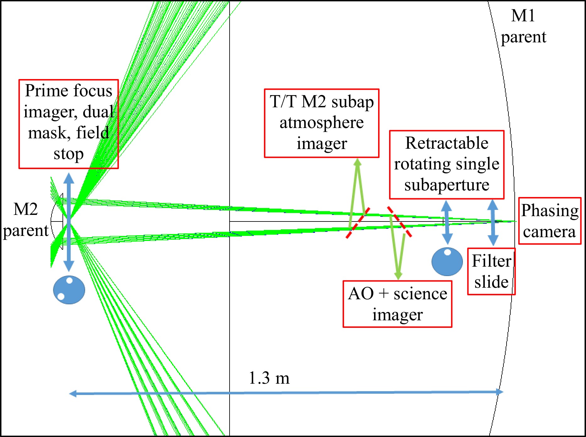
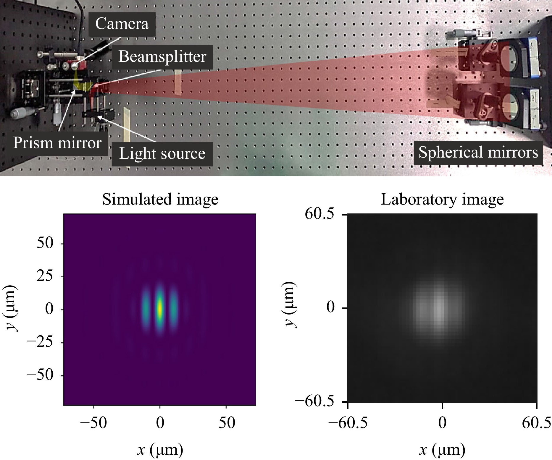
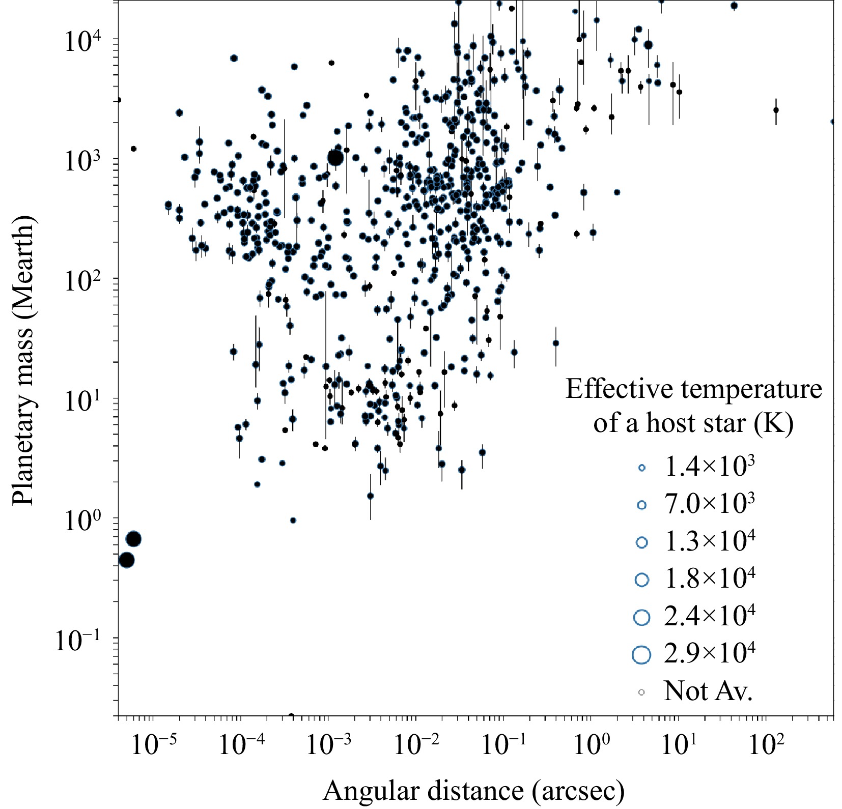
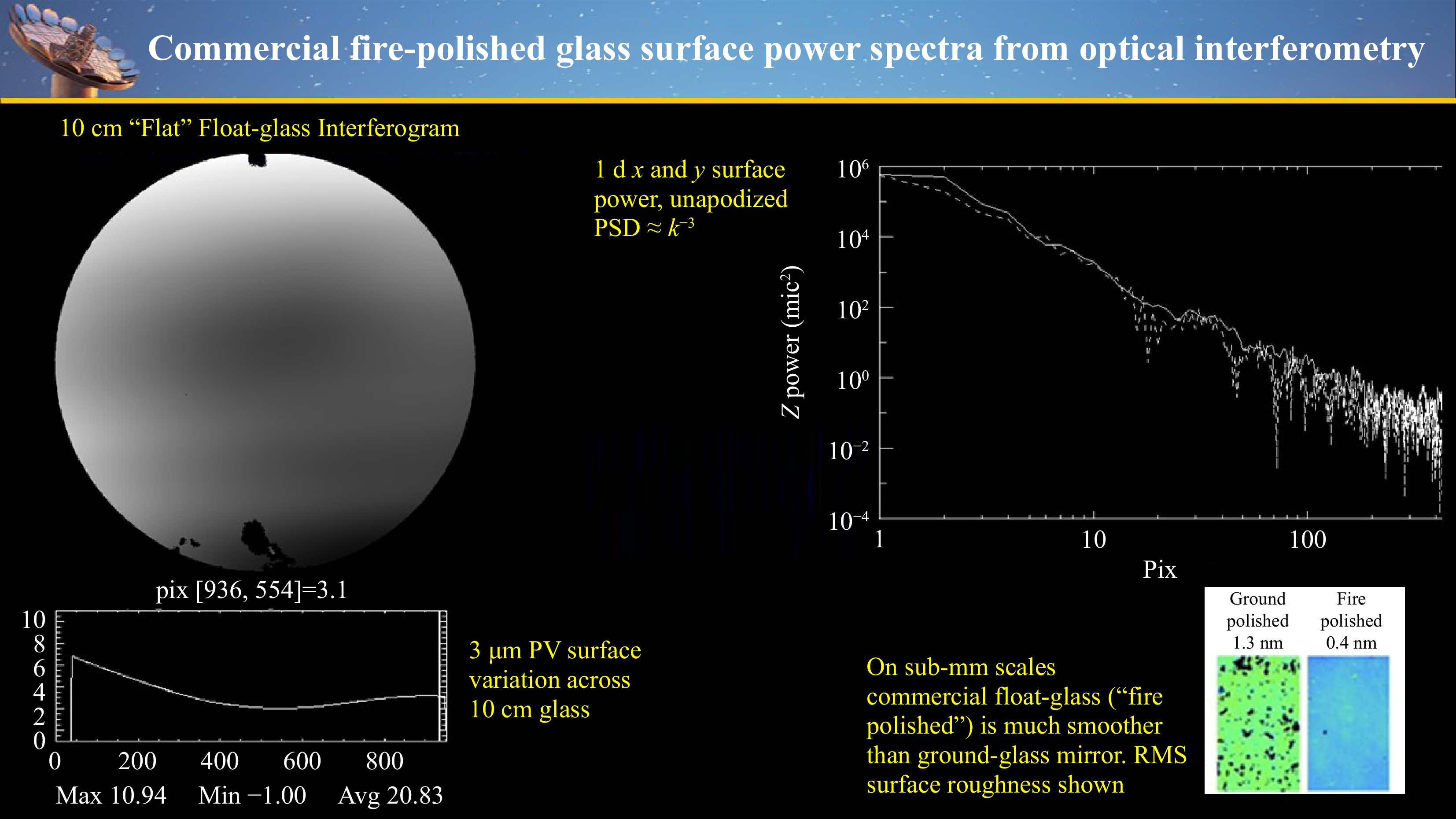
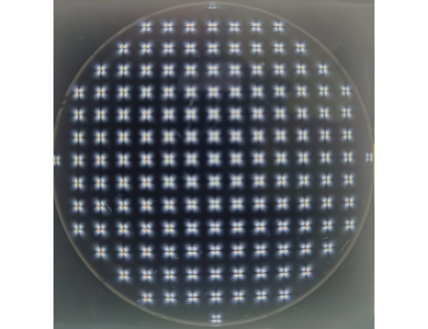
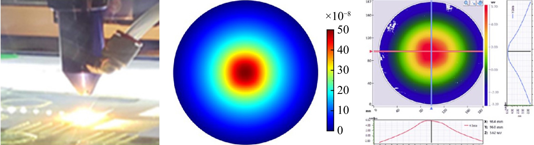
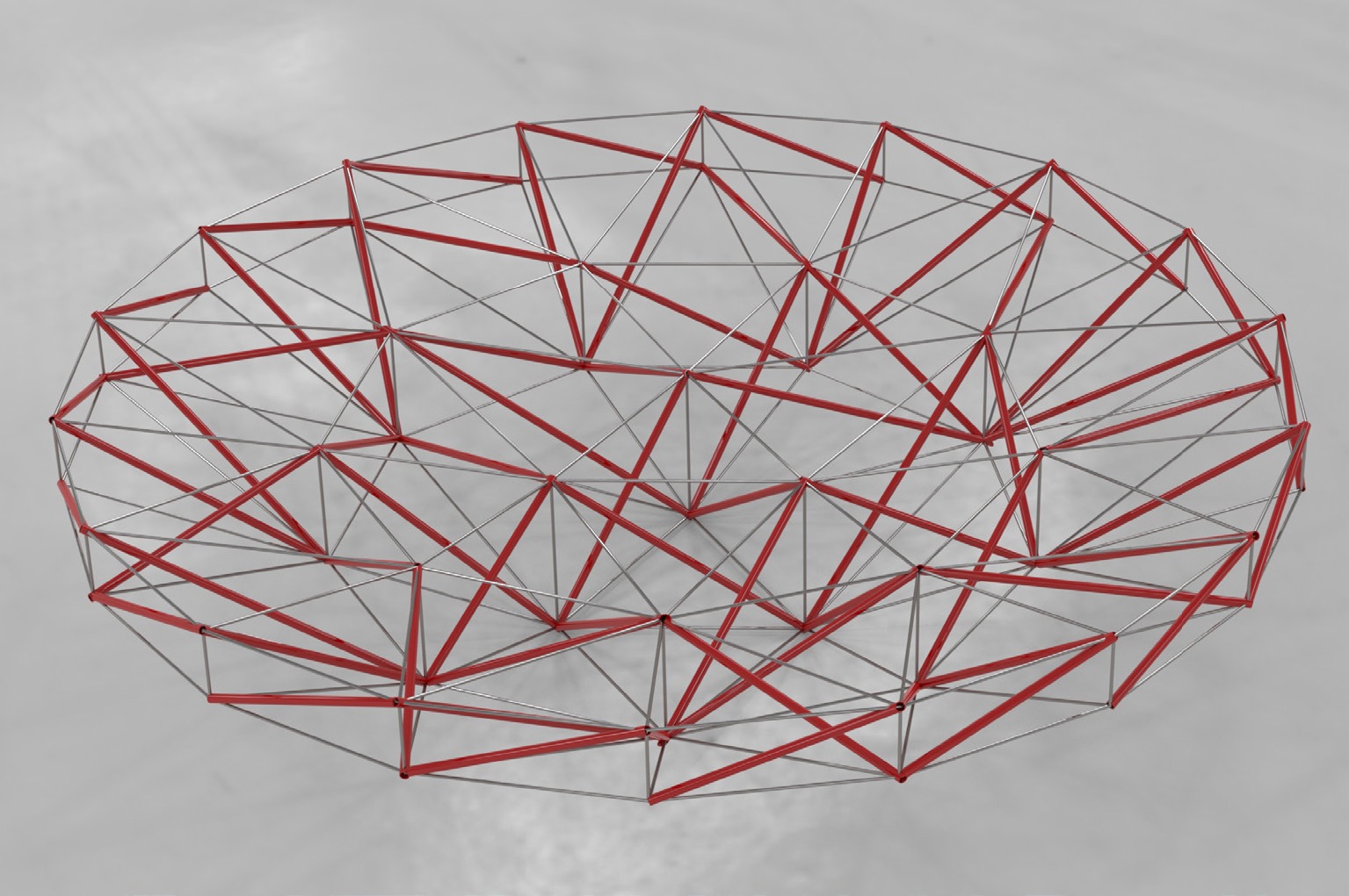
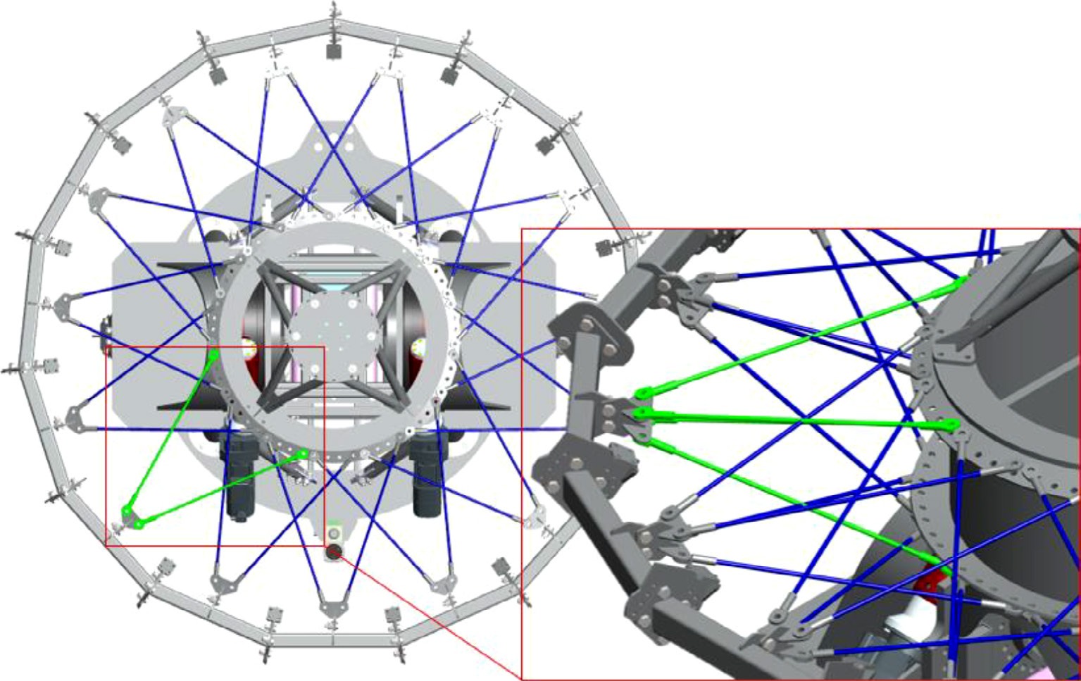
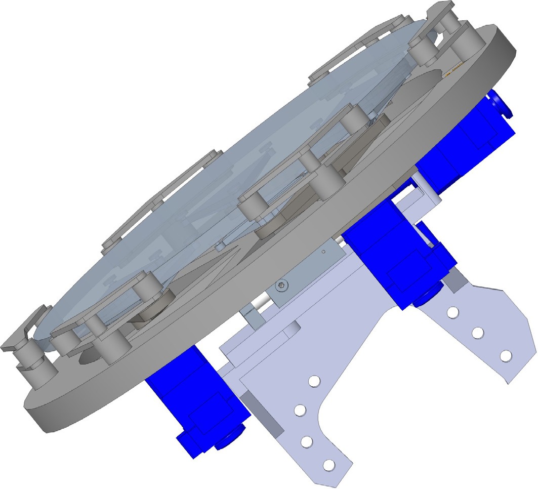
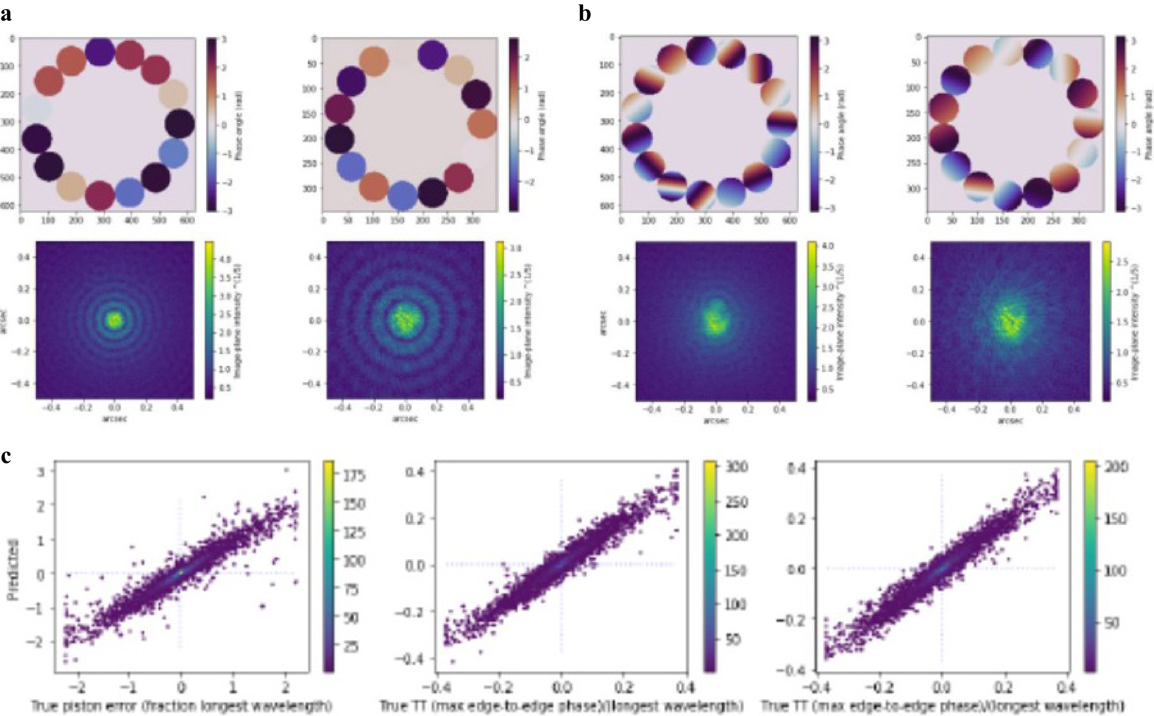
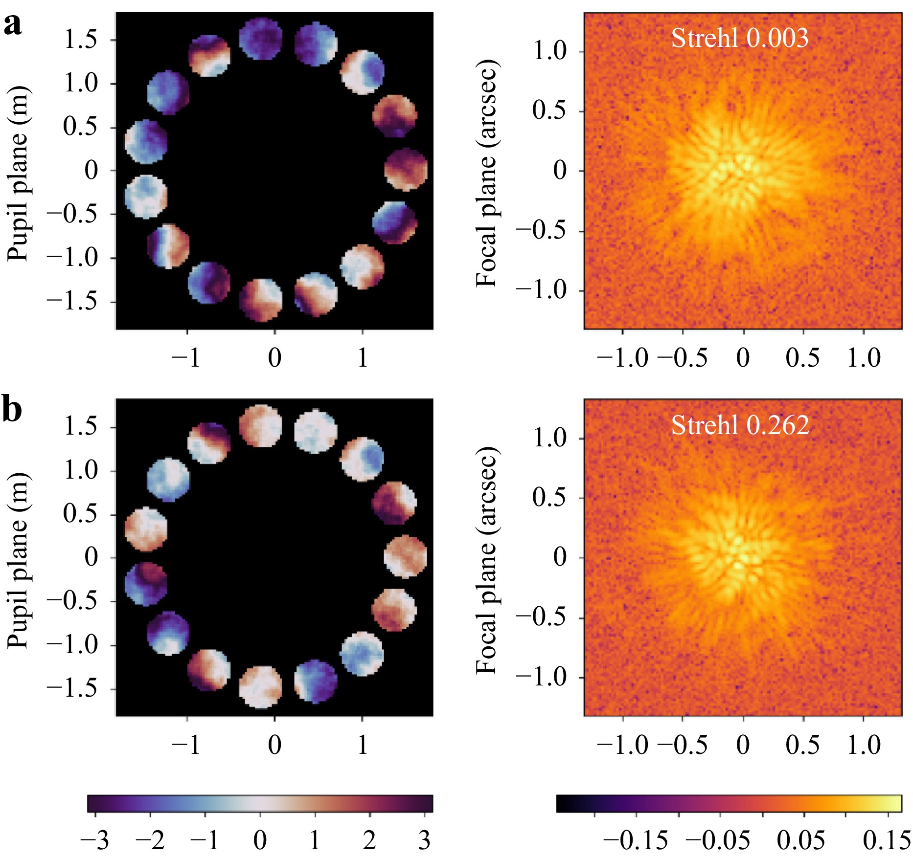
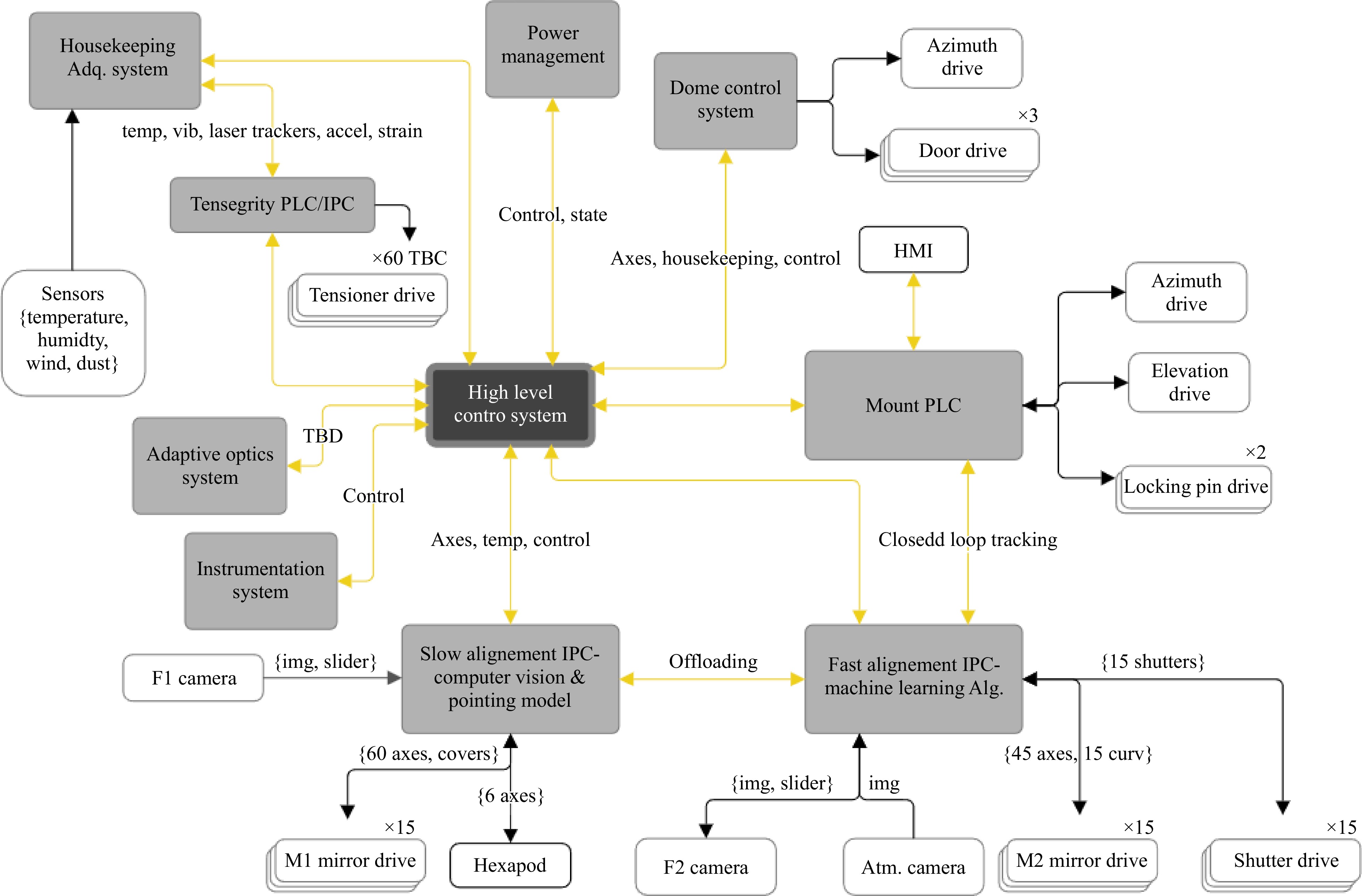
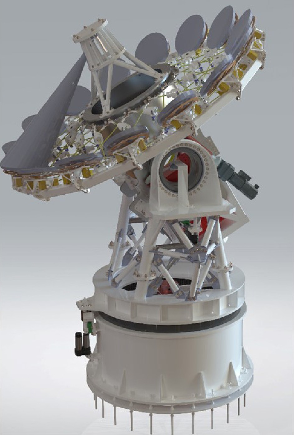
The largest ground-based telescopes will be much larger than their space-based counterparts far into the future. Remote sensing problems that can take advantage of active and adaptive wavefront control that correct the incoming atmospherically distorted optical wavefront can benefit from very large ground-based telescopes that have other important advantages. For example, their much lower cost (typically one or two orders of magnitude less) and shorter time-to-completion can be compelling. For optical or IR problems that require high angular resolution and large photometric dynamic range we suggest that techniques that make use of photonics, machine learning, or additive manufacturing may even enable less expensive specialized telescopes that are larger than what astronomers are currently building. The Instituto de Astrofísica de Canarias (IAC) recently began a 5 year program with support from the European Union called the Laboratory for Innovation in Opto-mechanics. Its goal is to show how technology innovations can enable less costly and larger telescopes, in particular, aimed at the problem of finding extrasolar life within a few parsecs of the Sun.

Published. 2025, 6(3)
: 474-485
doi: 10.37188/lam.2025.064
Meta-holograms, the computer-generated holograms assisted with nano-structured metasurfaces, promise efficient recording of light at the nanoscale. Adopting the multiplexing principle further bestows meta-holography with superb capacity for information storage and imaging applications. However, conventional meta-holograms mostly employ a single physical dimension to multiplex the holograms with incomplete light modulation, which imposes critical limitations on holography fidelity. To address this challenge, here we propose and experimentally demonstrate multi-dimensional multiplexing meta-holograms using full-modulation dielectric geometric-phase metasurfaces. Such metasurfaces enable simultaneous, independent, and arbitrary control of the amplitude, phase, and polarization of spatial light based on the geometric-phase principle, with broadband properties. Thanks to the full-modulation principle, the metasurfaces enable the meta-holograms to multiplex multiple holographic images with engineered patterns, polarizations, and directions, depending on the particular input and output conditions. Compared with the holograms acquired with incomplete light modulation, the designed meta-holograms not only inspire an accurate high-capacity information integration with low crosstalk and ideal energy uniformity, but can also facilitate complex multi-dimensional optical information broadcasting, anti-counterfeit, and encryption in compact optoelectronic devices. This work provides a full-modulation metasurface strategy for robust and scalable multi-dimensional multiplexing meta-holography.


Published. 2025, 6(3)
: 486-503
doi: 10.37188/lam.2025.059
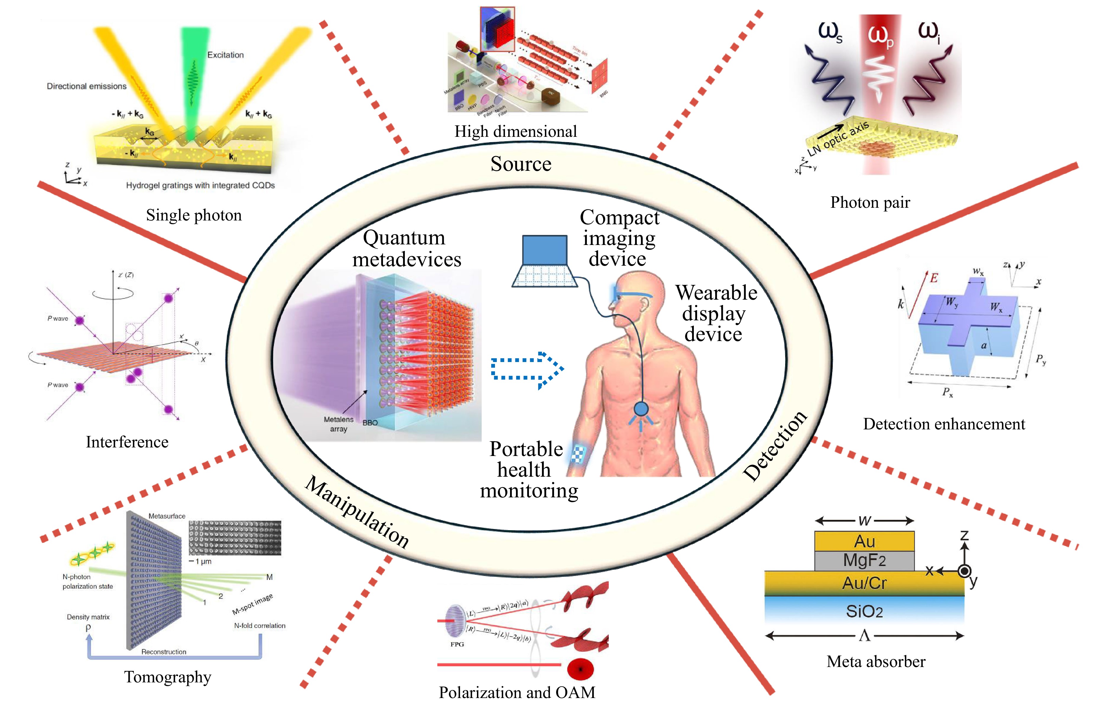
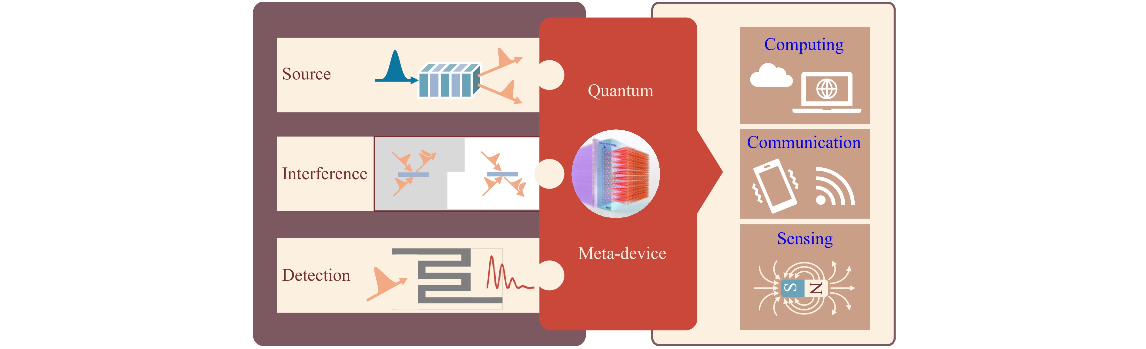
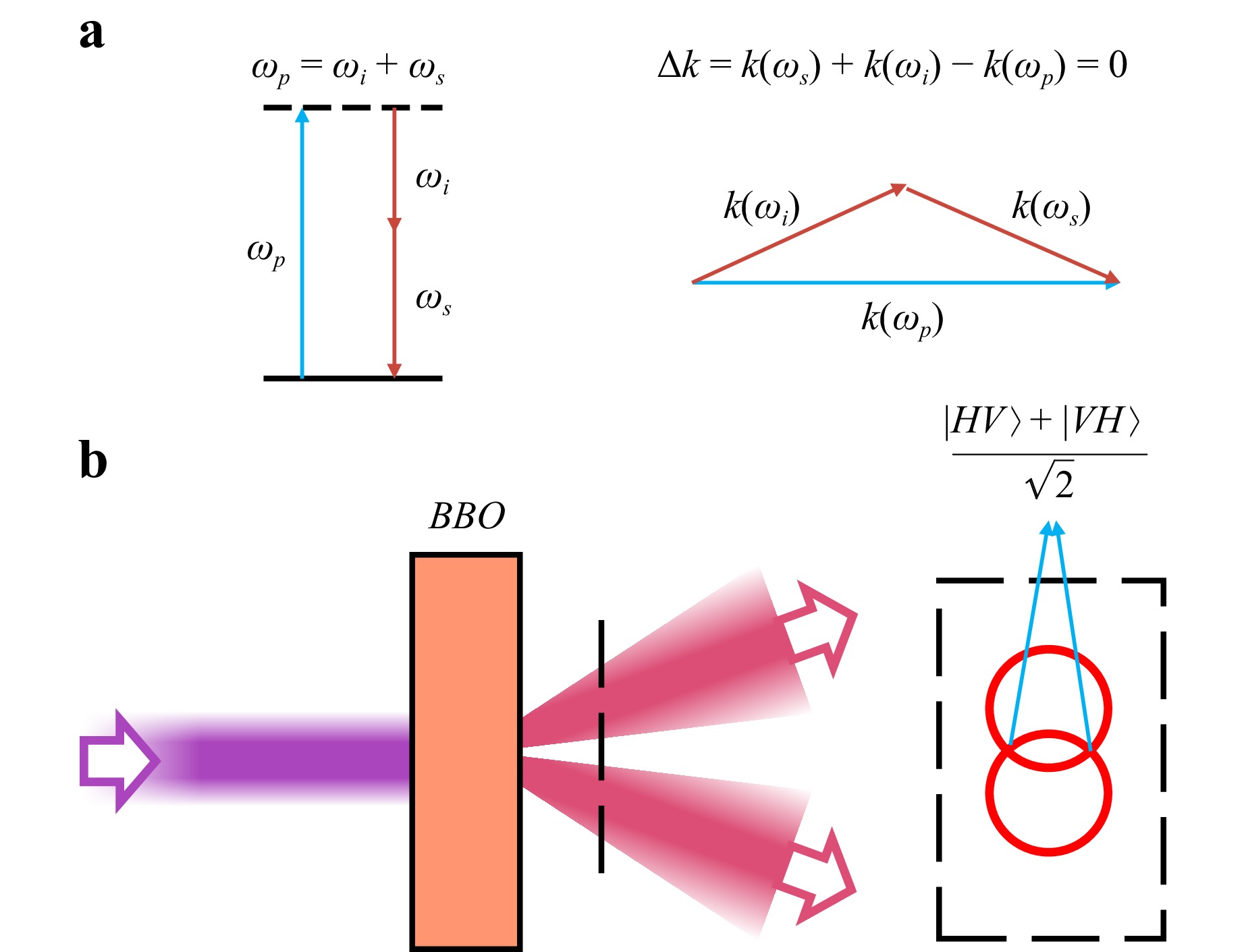
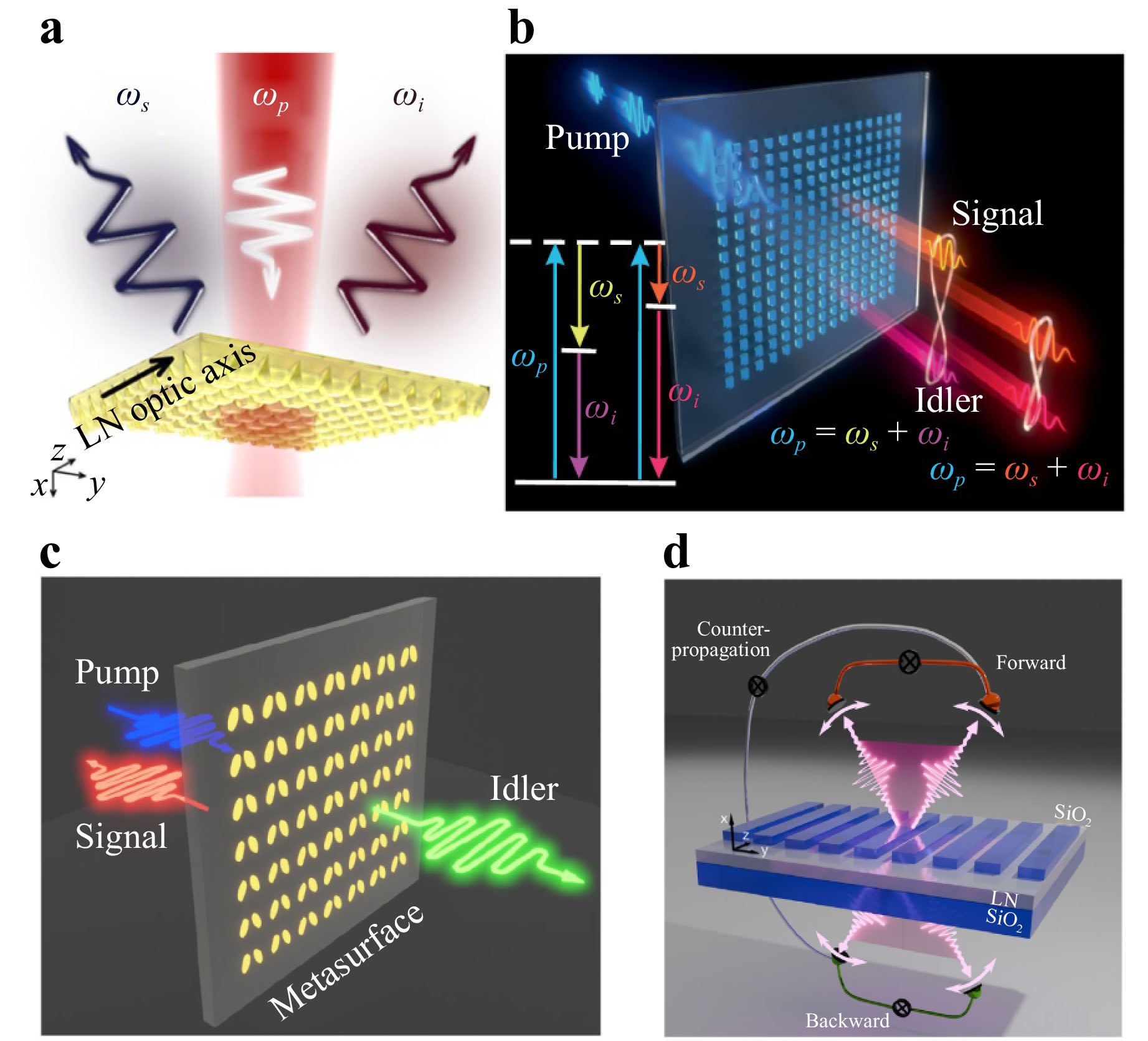
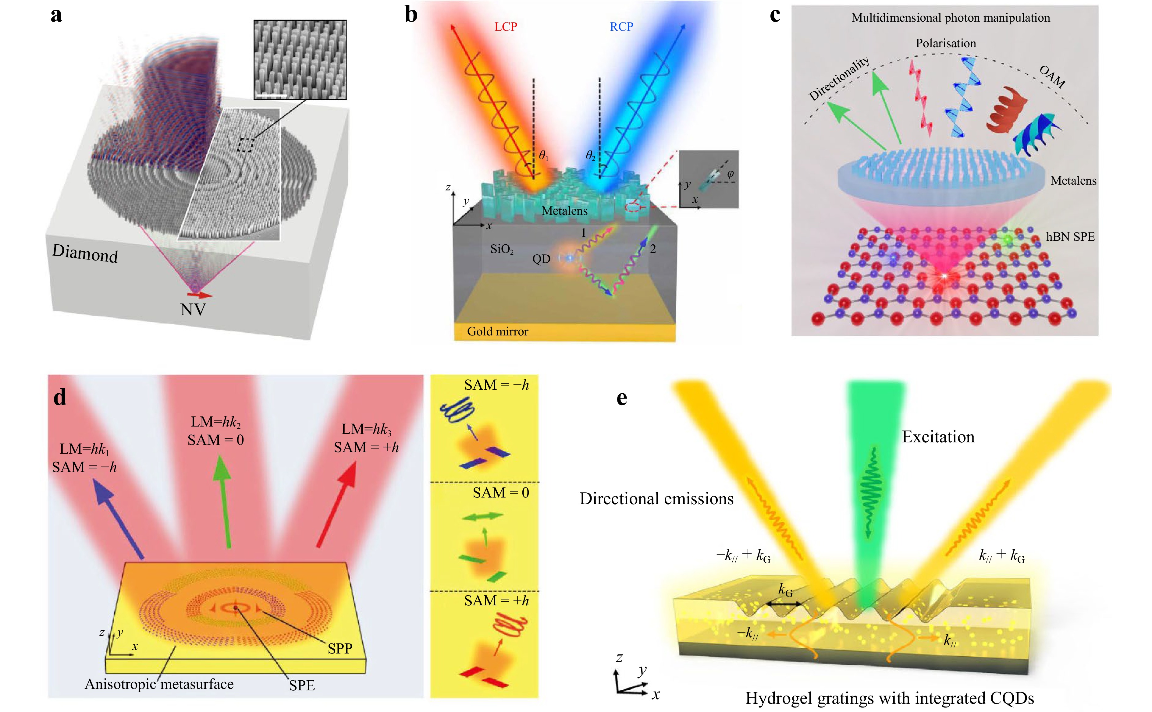
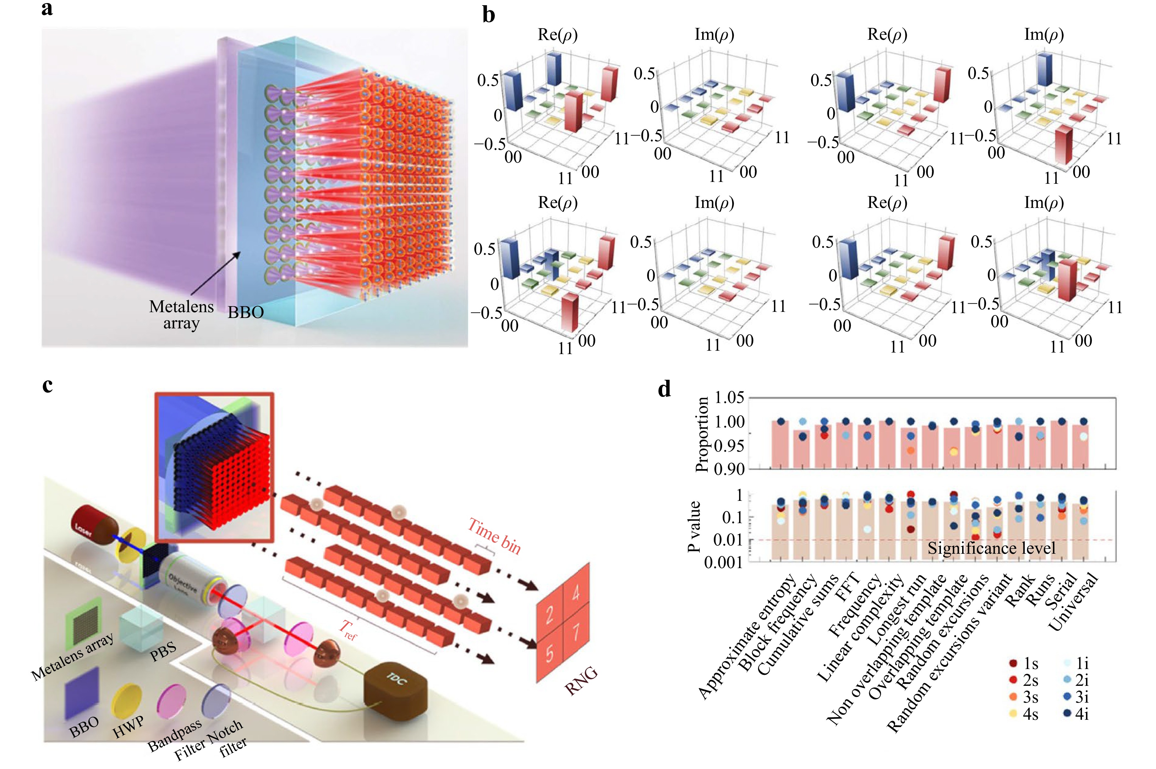
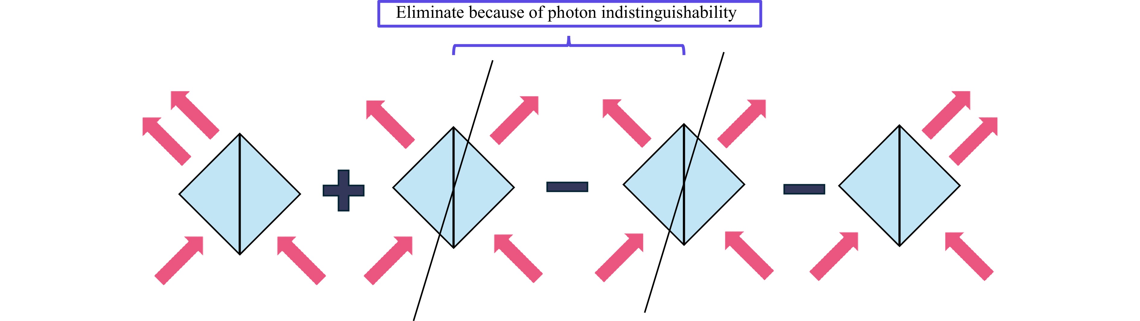
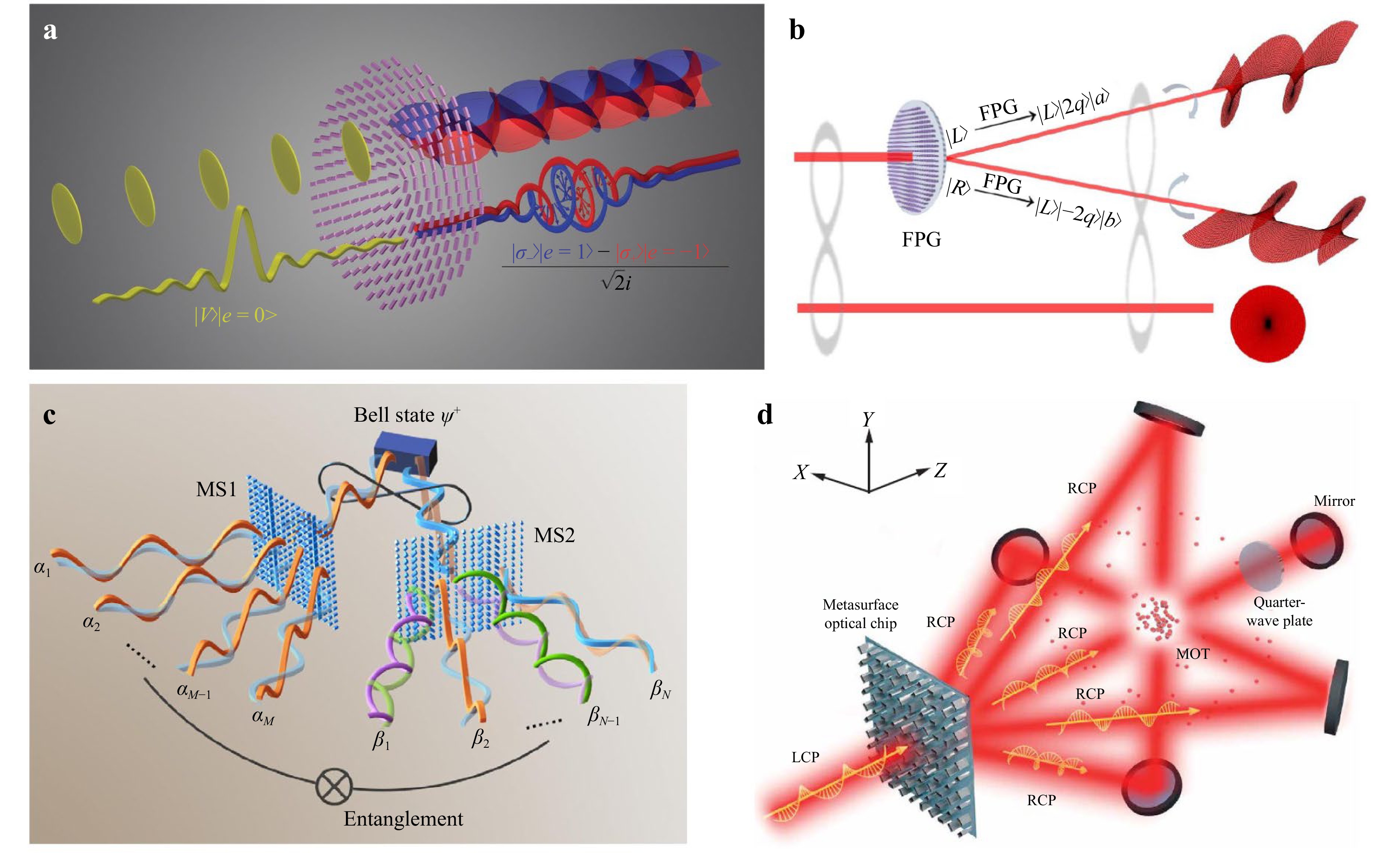
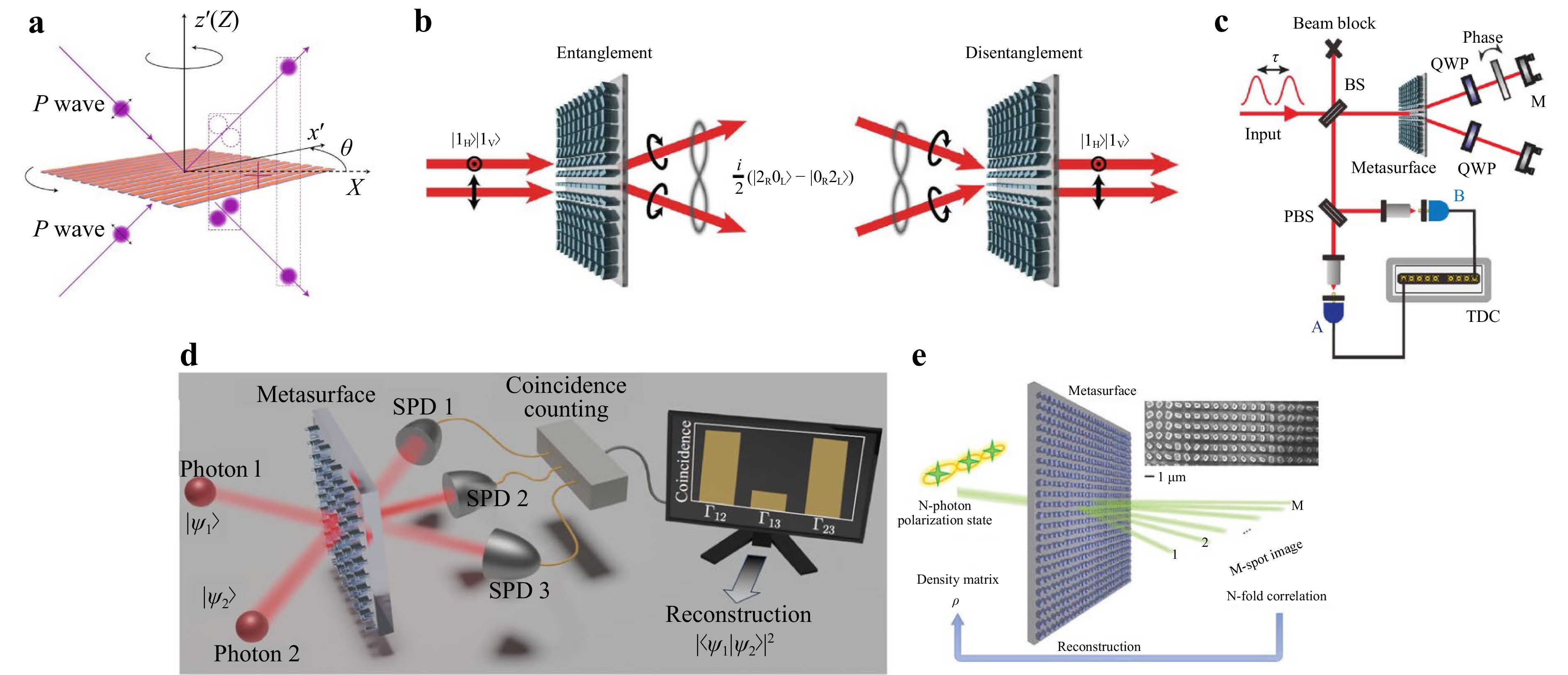
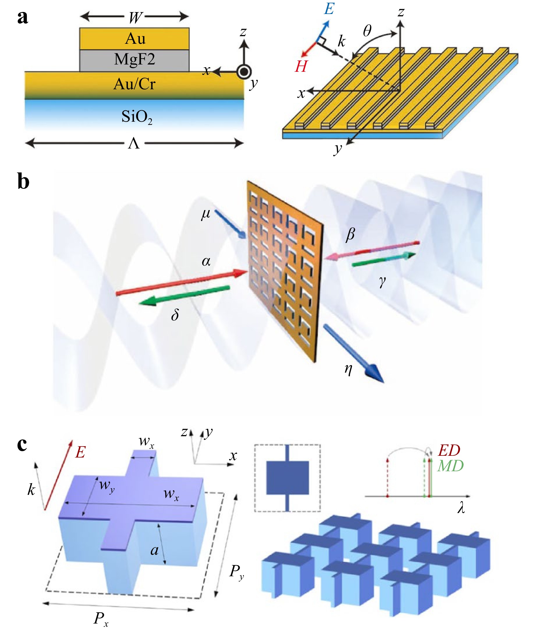
Meta-devices, known for their capability to manipulate light fields at a subwavelength scale, have gained significant traction in the realm of quantum photonics in recent years. They are being utilized in miniaturized applications such as the preparation of quantum light sources and the control and detection of quantum states. In this review, we provide a systematic explanation of the working principles and notable applications of meta-devices in quantum optical information processing, while also outlining potential directions for the future development of quantum meta-devices.
Published. 2025, 6(3)
: 504-521
doi: 10.37188/lam.2025.058
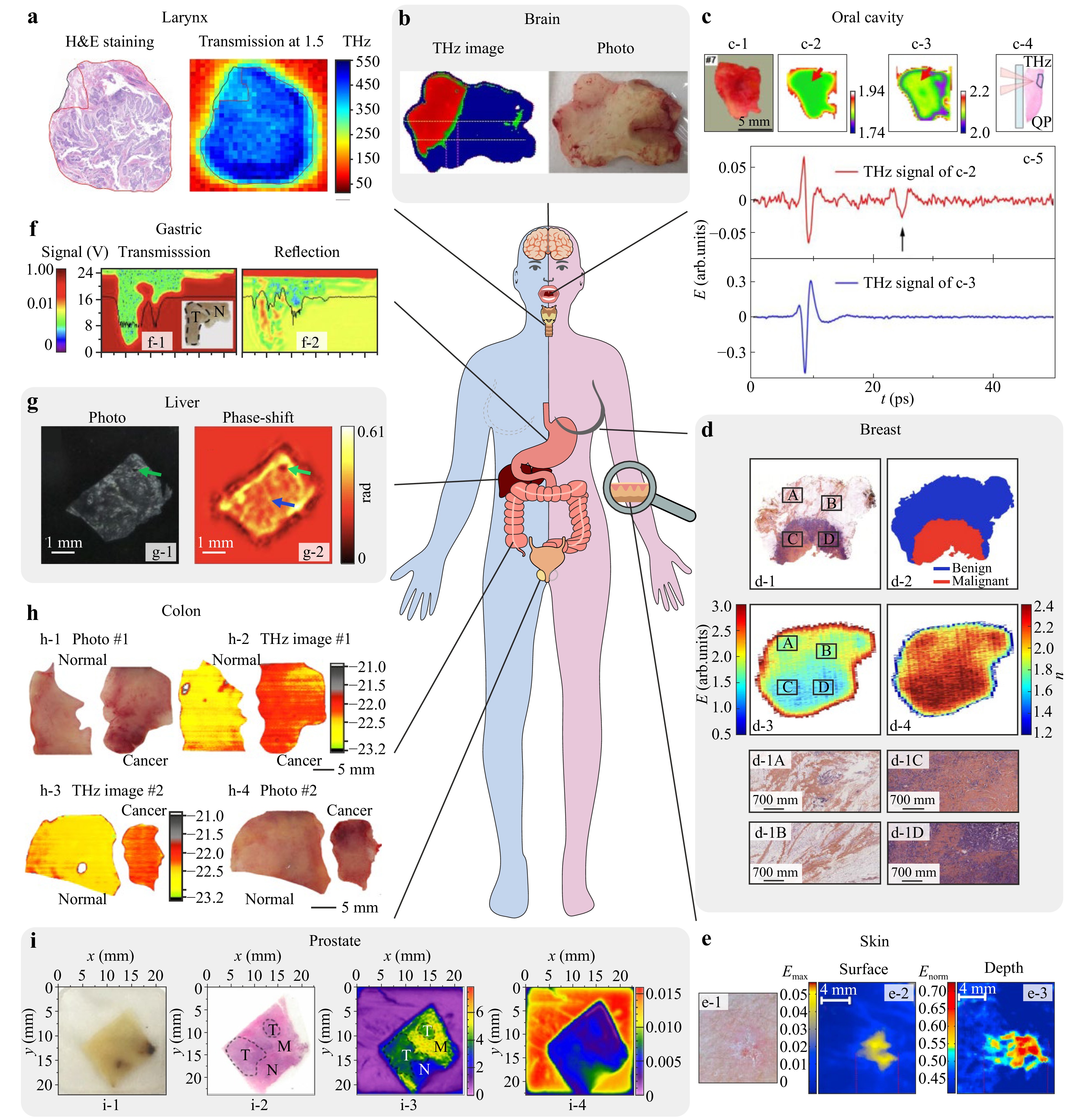
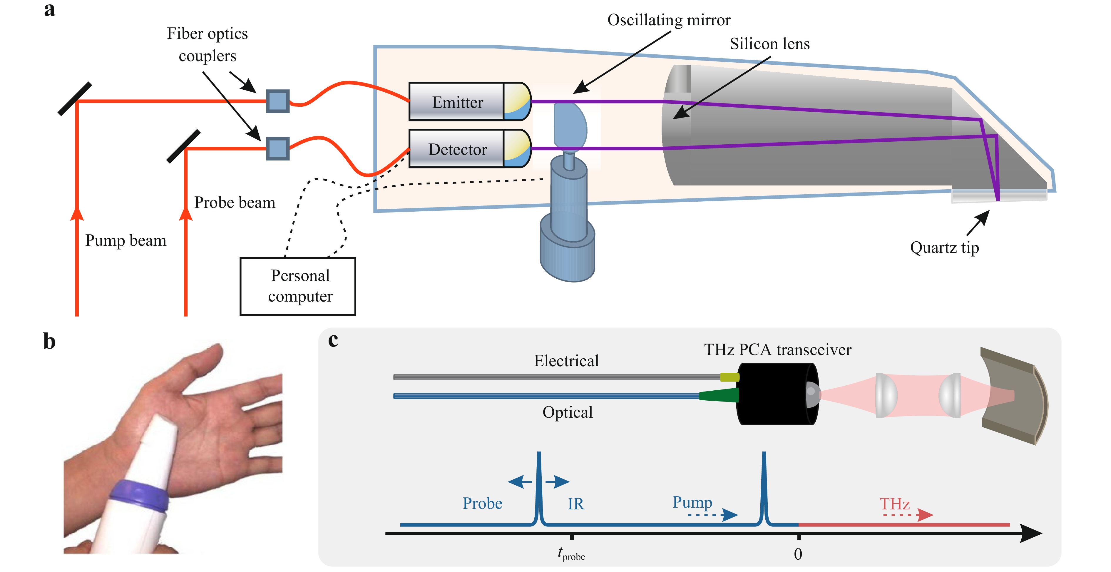
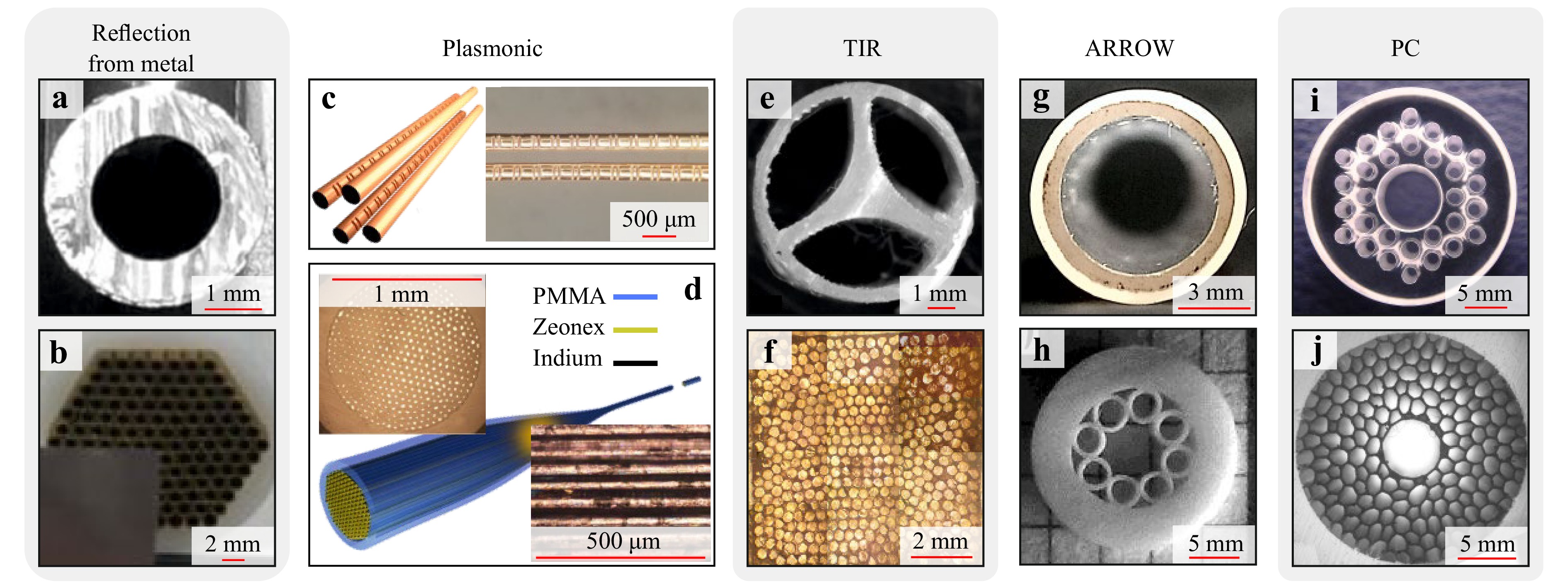
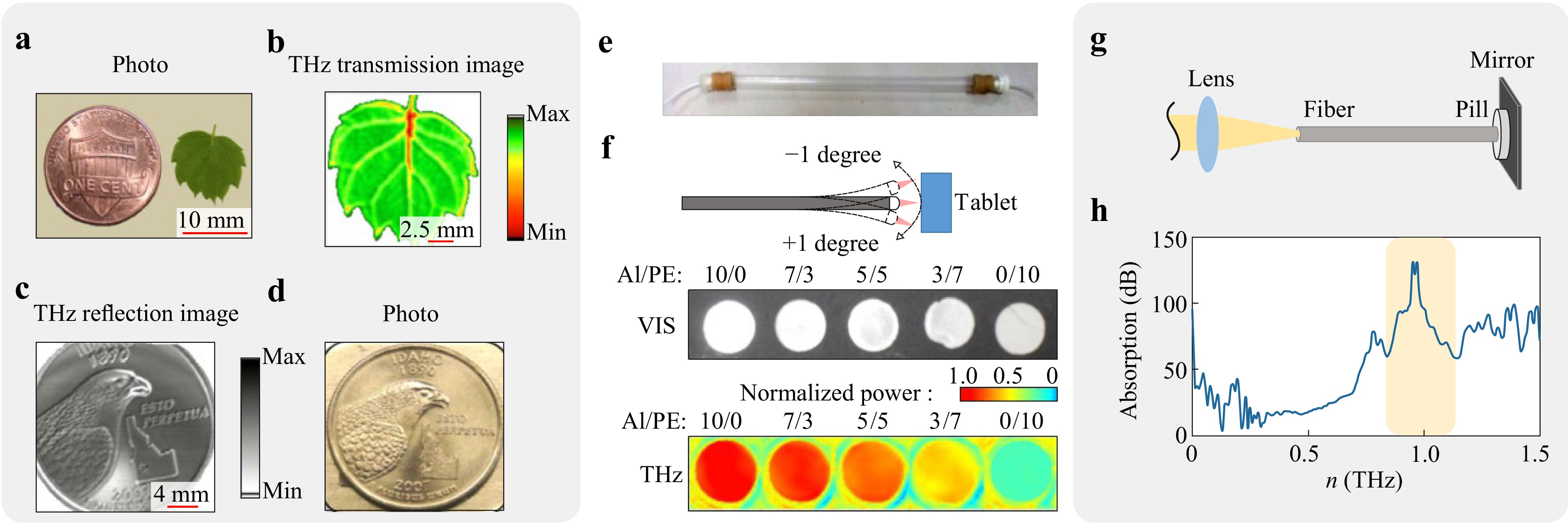
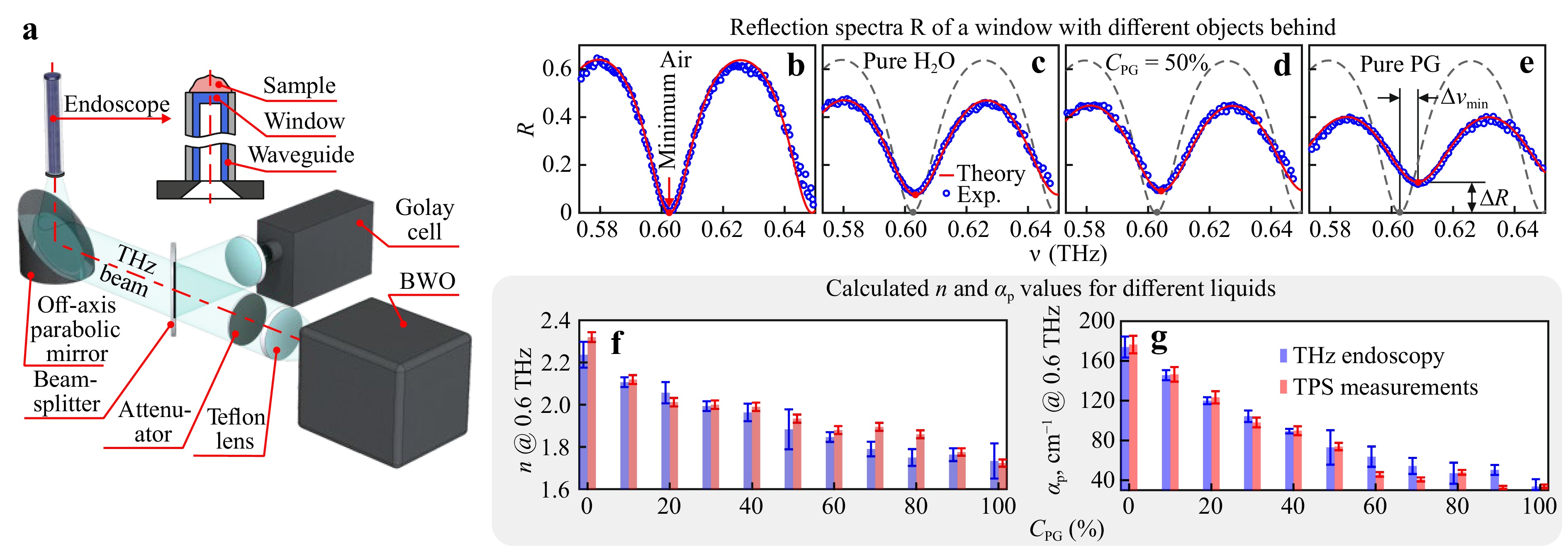
Although terahertz (THz) spectroscopy and imaging offer a variety of applications in medical diagnosis of malignant and benign neoplasms, their translation into clinical practice is hampered by the absence of endoscopic systems capable of sensing the THz optical properties of the hard-to-access tissues. In this review, we focus on recent attempts to address this challenge. To better highlight the need for THz endoscopes, we start with a brief overview of THz medical applications, with an emphasis on neoplasms diagnosis. We then consider the two existing principles of THz endoscopy. The first uses the fiber-coupled THz photoconductive antennas (PCAs) for the THz generation and detection in close proximity to a hard-to-access object, where optical fibers are applied to flexibly deliver the laser pump and probe beams to the THz emitter and detector. The key technology of the second approach is the THz optical fibers capable of delivering the THz waves to an analyte and then detecting the reflected and back-propagated THz signal. Despite this approach still lacking the efficient commercially available THz fiber optics, most recent developments pave the way to solve these problems. In this review, several notable examples of THz endoscopic systems based on different guiding mechanisms, material platform, and manufacturing strategies are discussed.
Published. 2025, 6(3)
: 522-545
doi: 10.37188/lam.2025.049
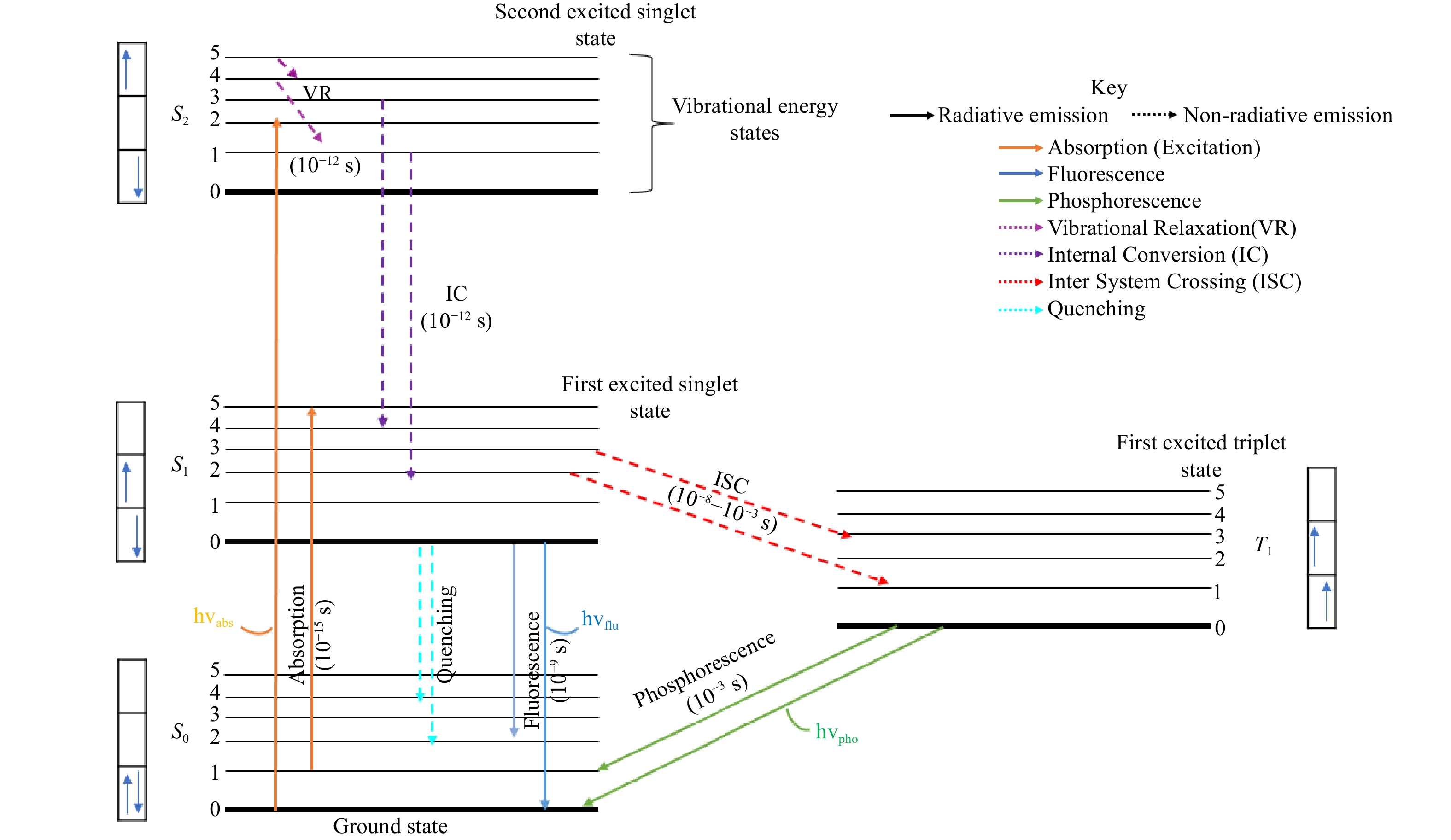
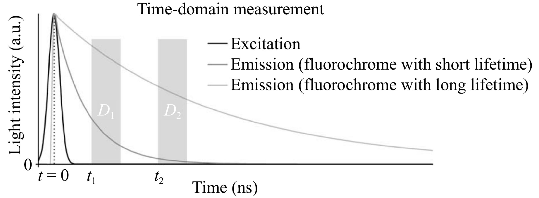
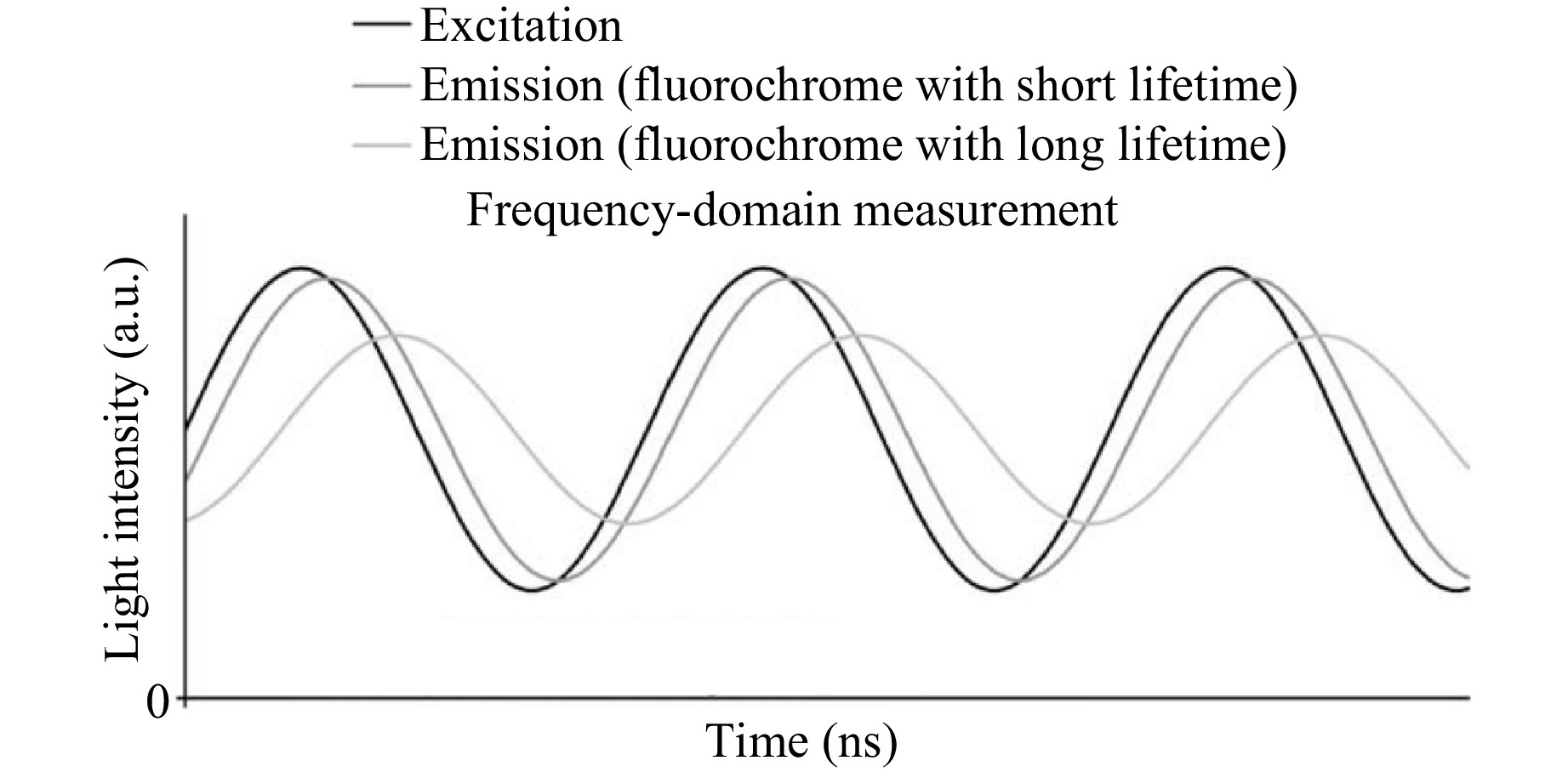
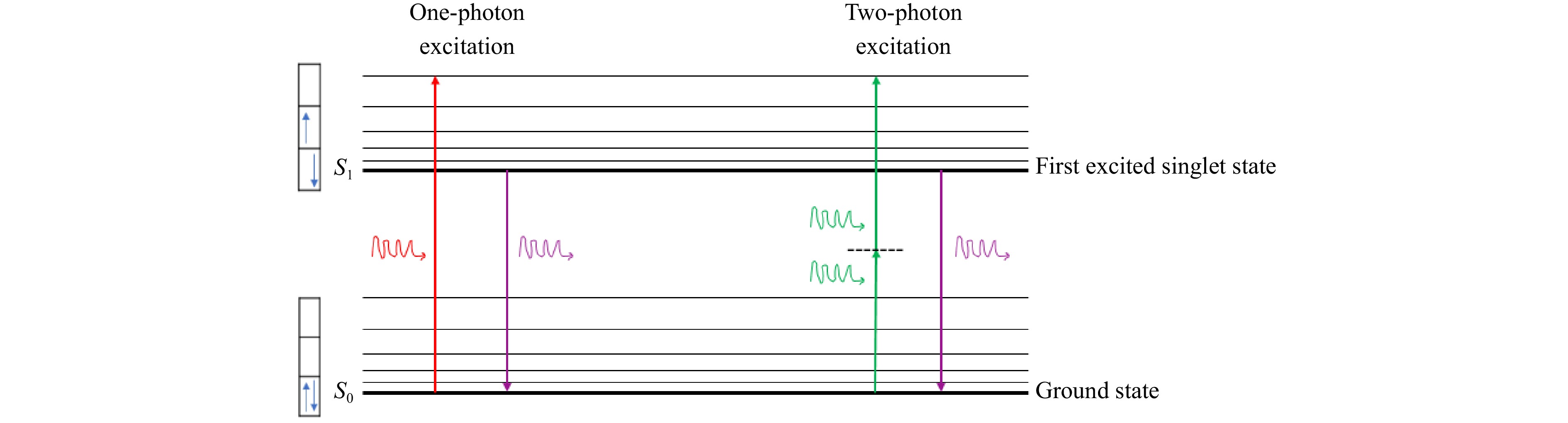
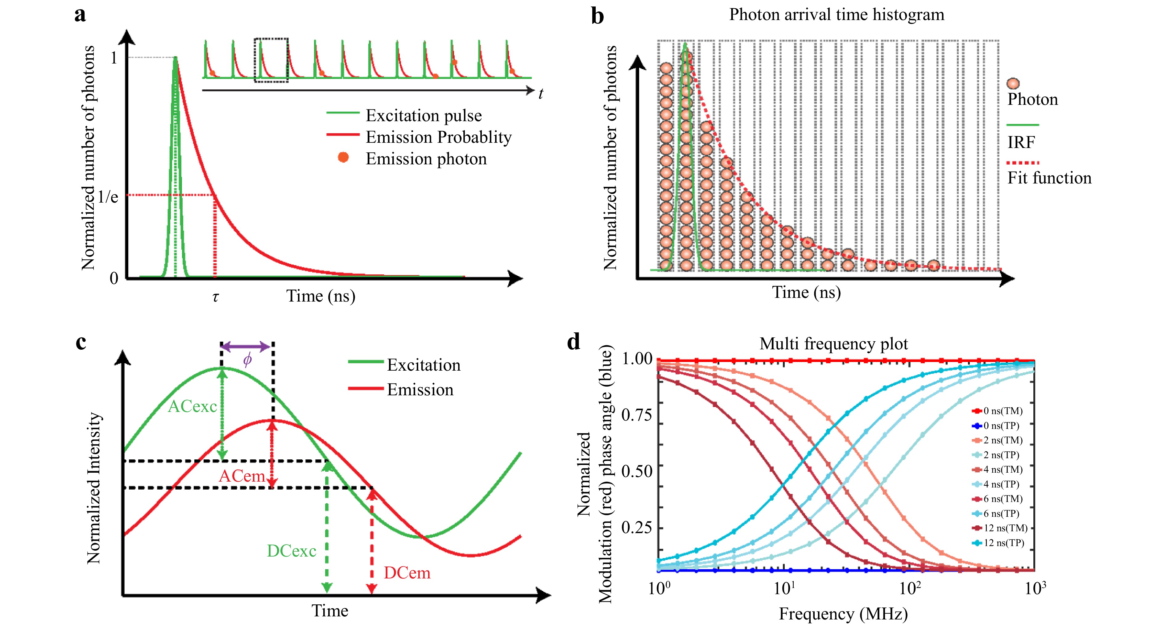
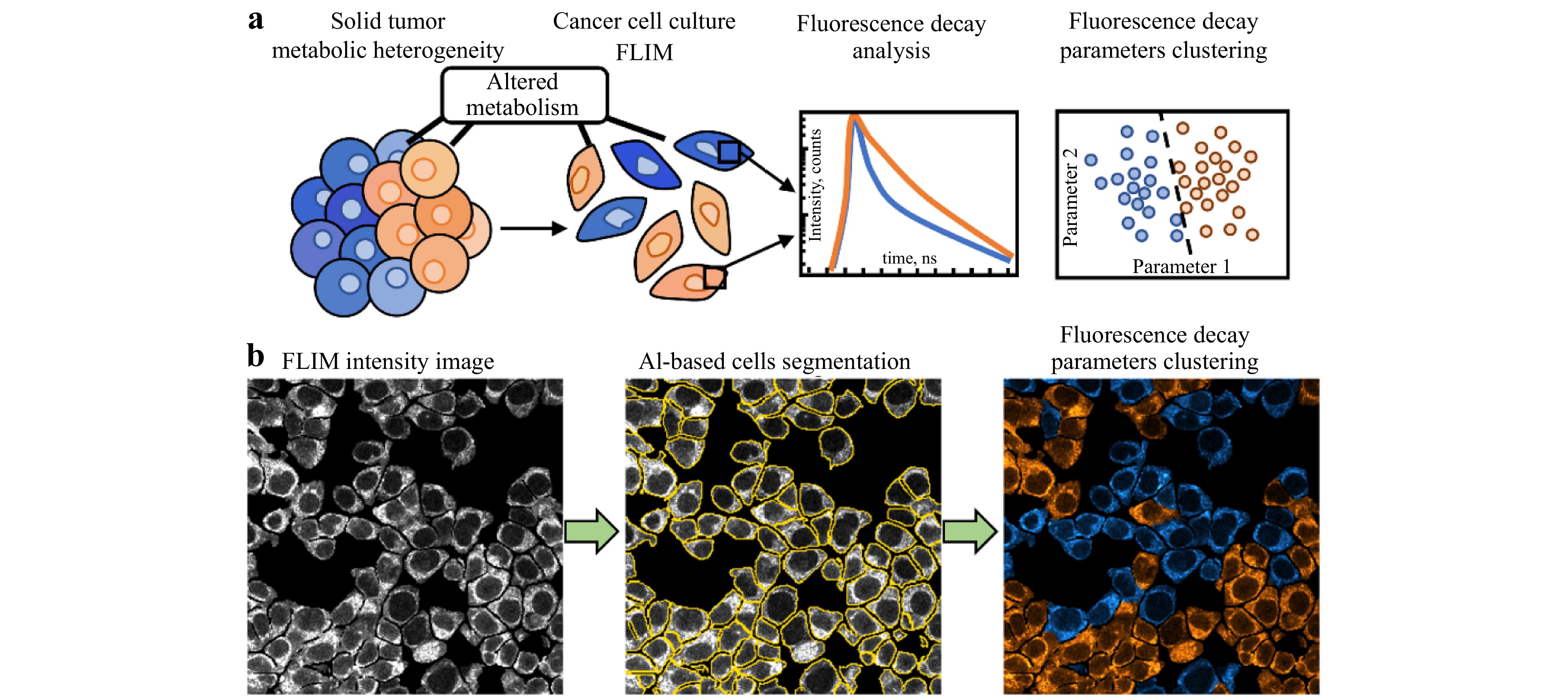
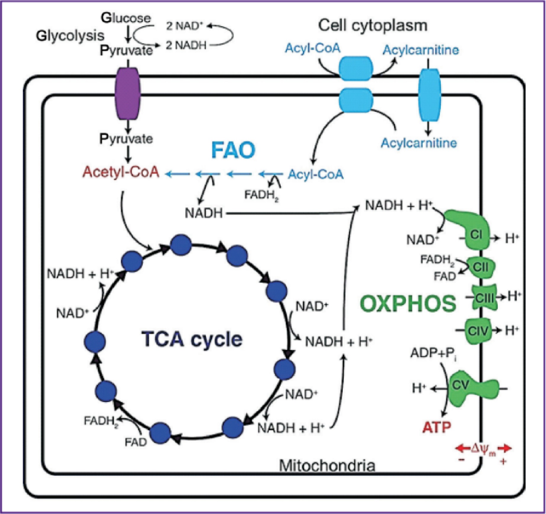
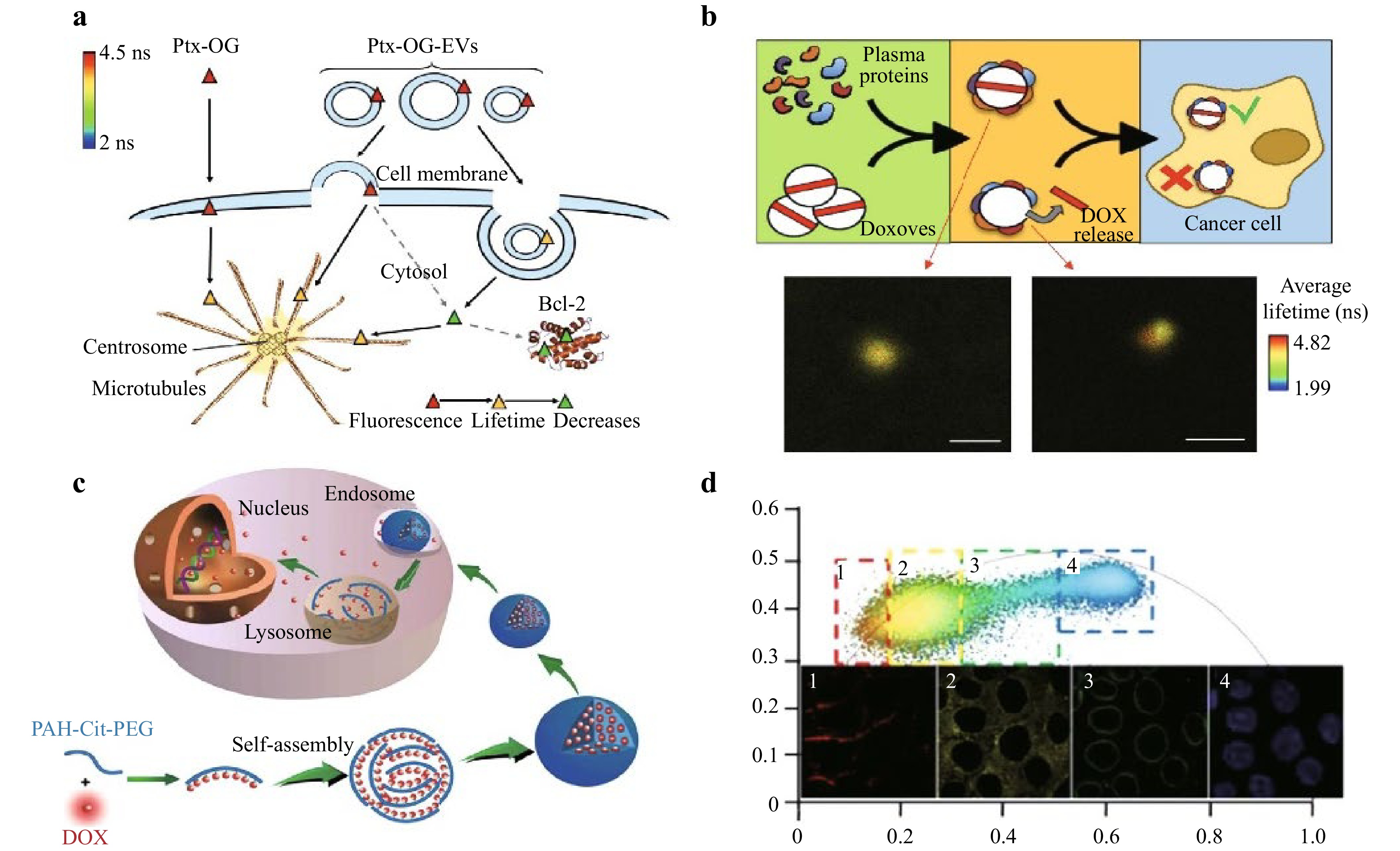
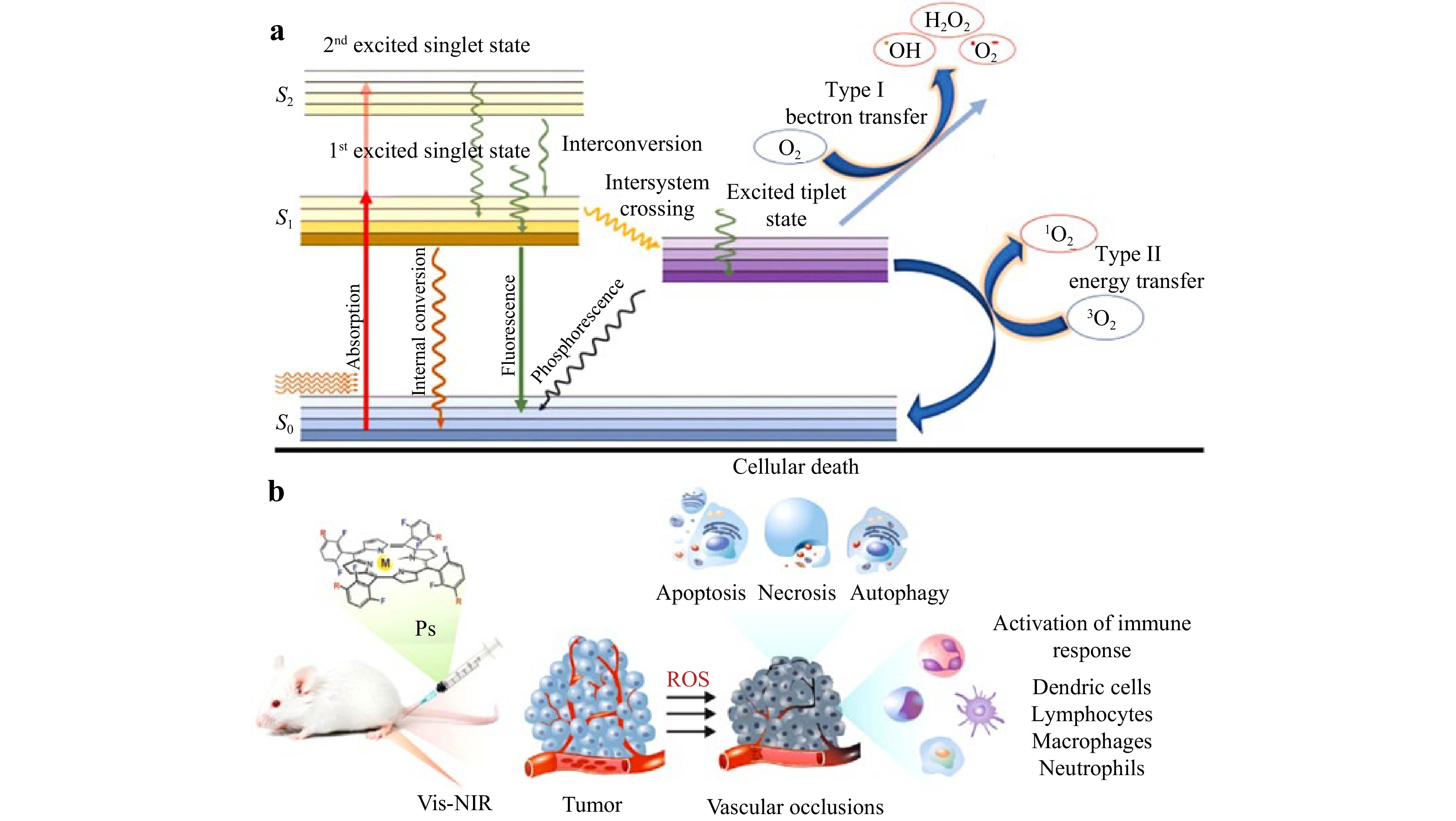
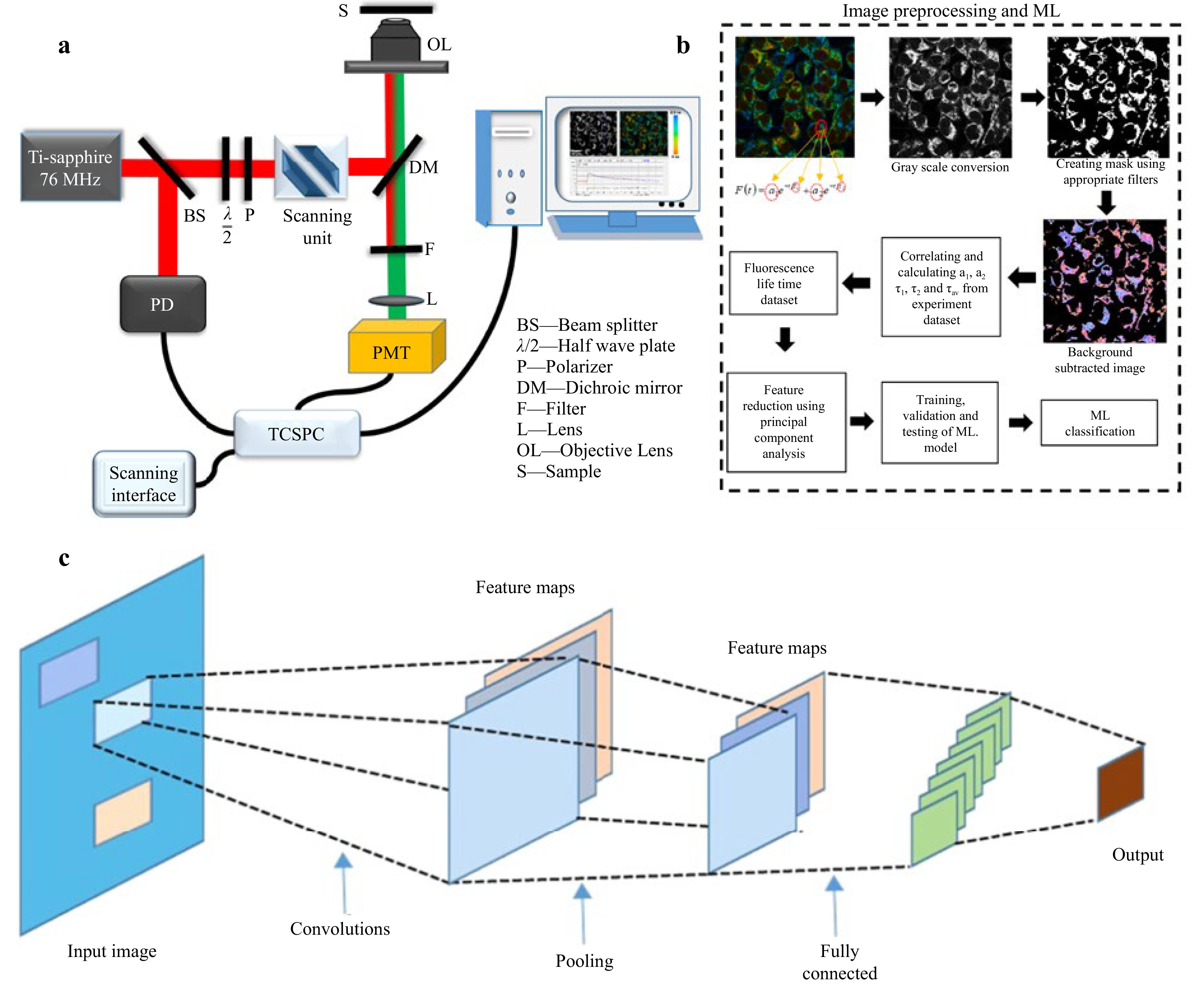
Fluorescence lifetime imaging microscopy (FLIM) has emerged as a transformative imaging technique in cancer research, offering quantitative insights into cellular metabolism, tumor microenvironments, and therapeutic responses. By measuring the fluorescence lifetimes of metabolic cofactors such as NADH and FAD, FLIM facilitates the analysis of cancer-specific metabolic reprogramming and heterogeneity. Integration with deep learning further enhances FLIM’s diagnostic and therapeutic potential, enabling high-resolution imaging, automated data analysis, and biomarker identification. This review provides a comprehensive overview of the principles and technological advancements of FLIM, highlighting its applications in cancer diagnostics, drug delivery, and therapy, as well as its integration with deep learning to increase imaging precision and data interpretation. Challenges such as high costs, high computational complexity, and the need for standardized imaging protocols are also addressed. By bridging FLIM with cutting-edge computational techniques, this review highlights its potential to revolutionize cancer research, paving the way for early diagnosis, personalized therapies, and deeper insights into tumor biology.
Published. 2025, 6(3)
: 546-574
doi: 10.37188/lam.2025.048
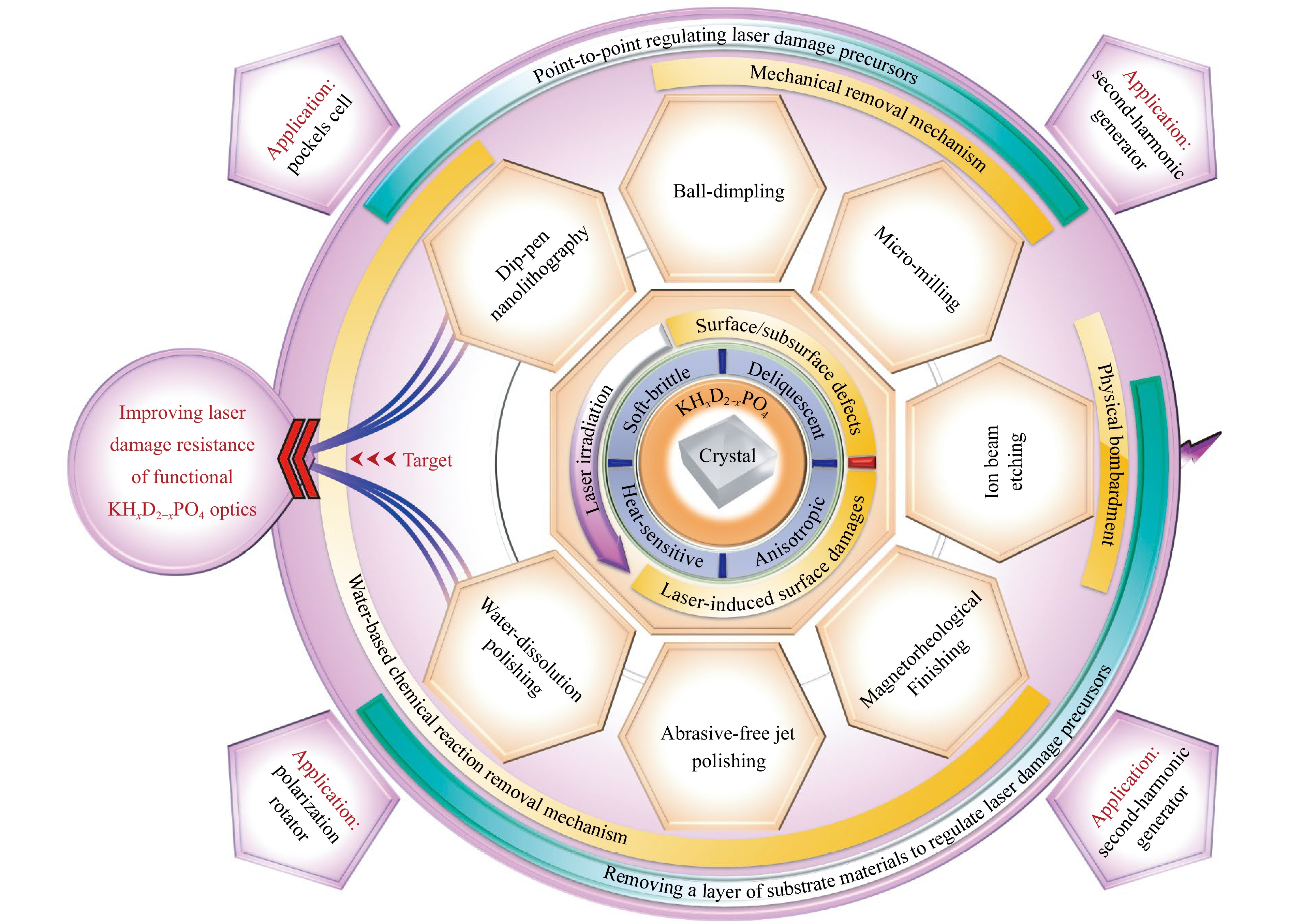
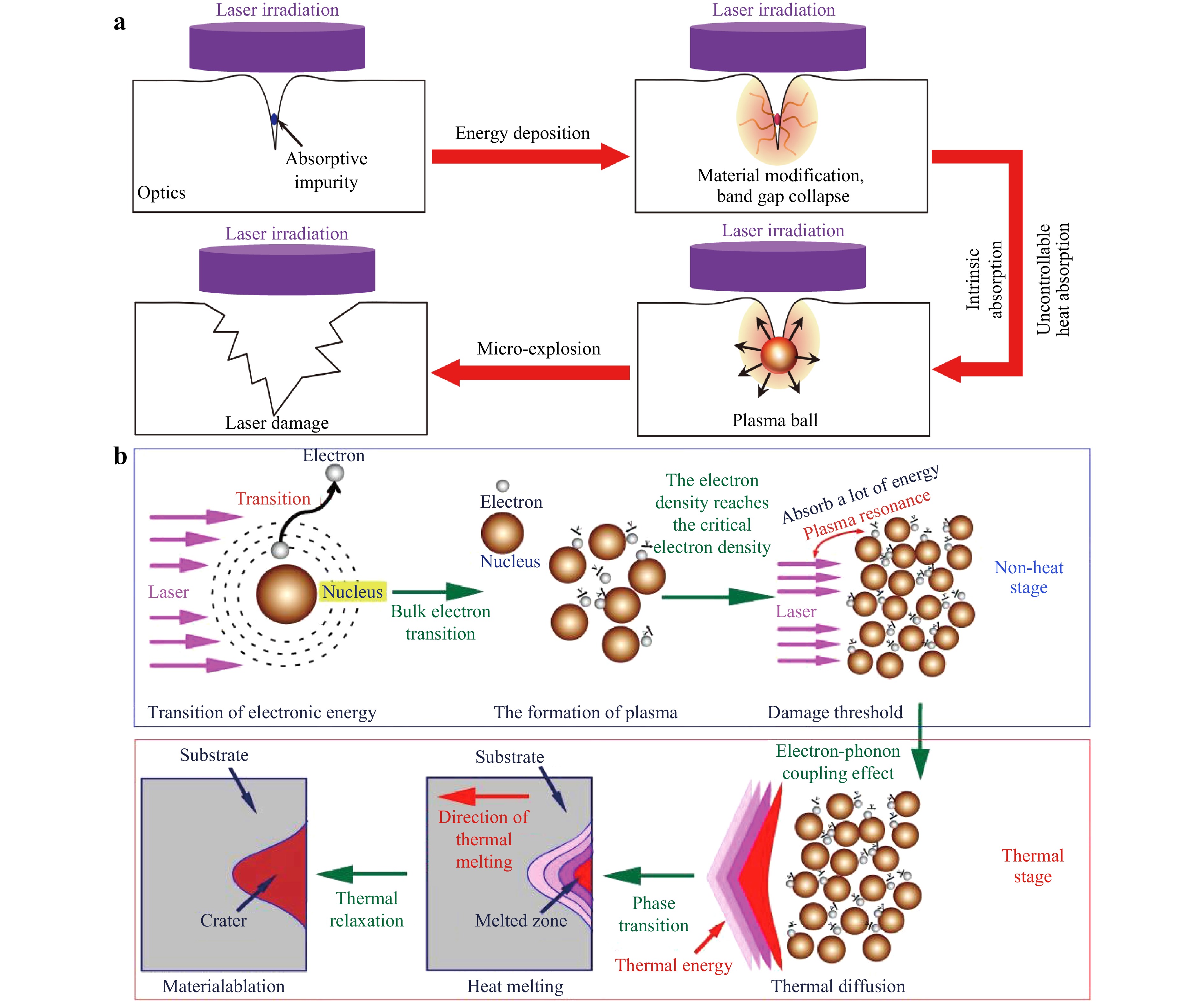
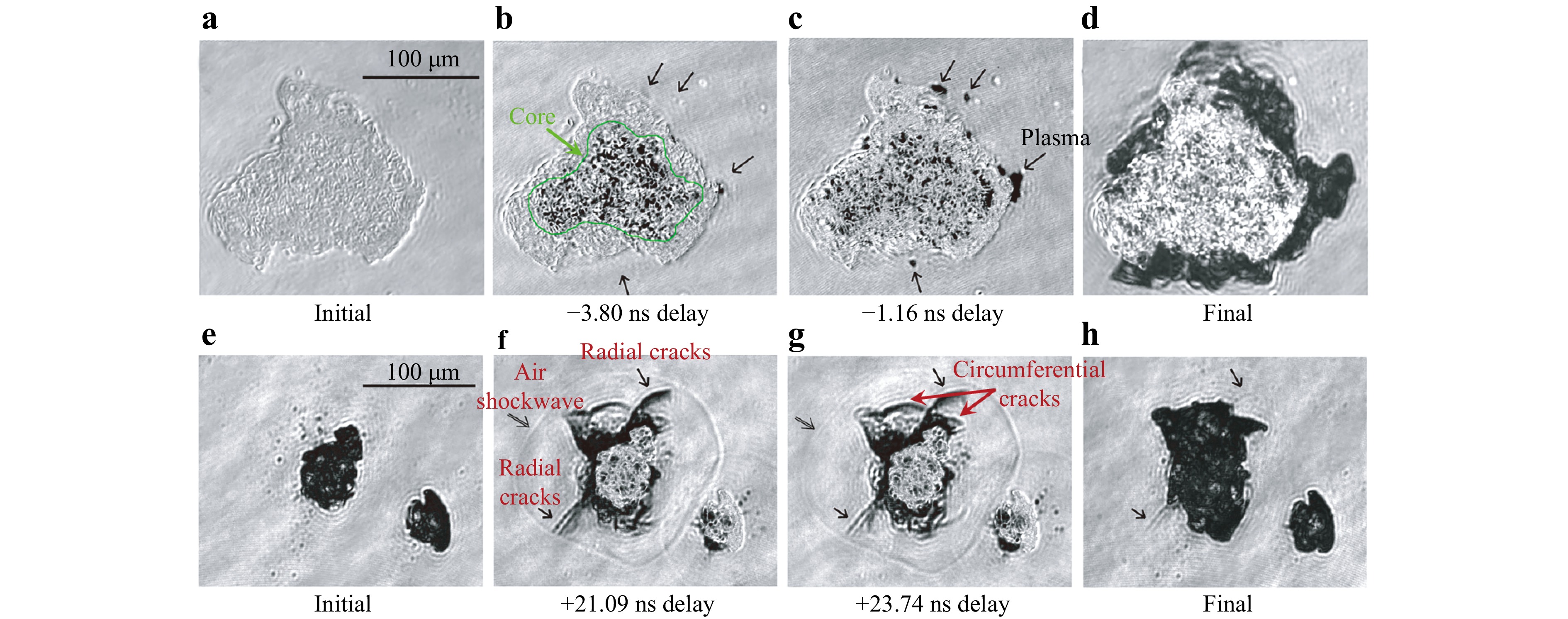
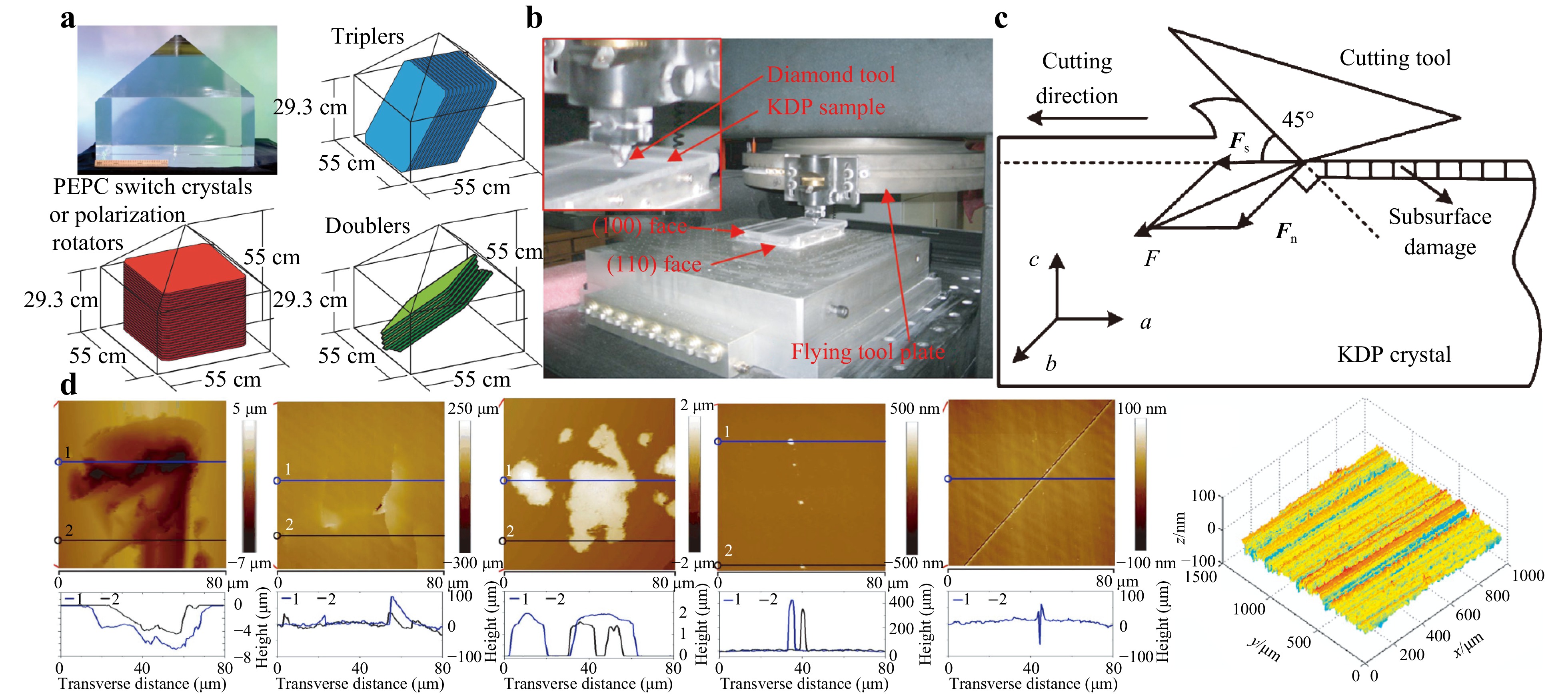
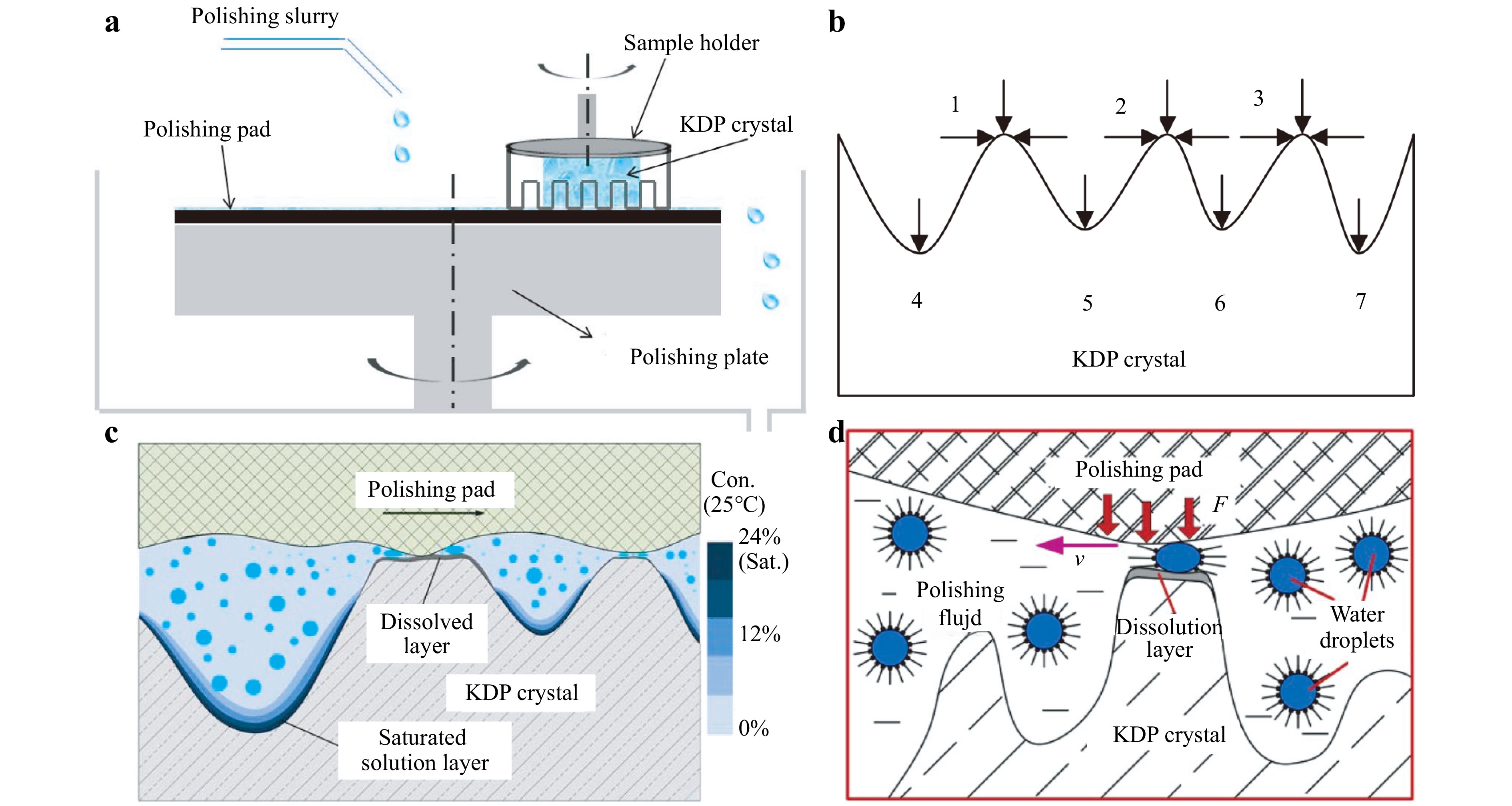
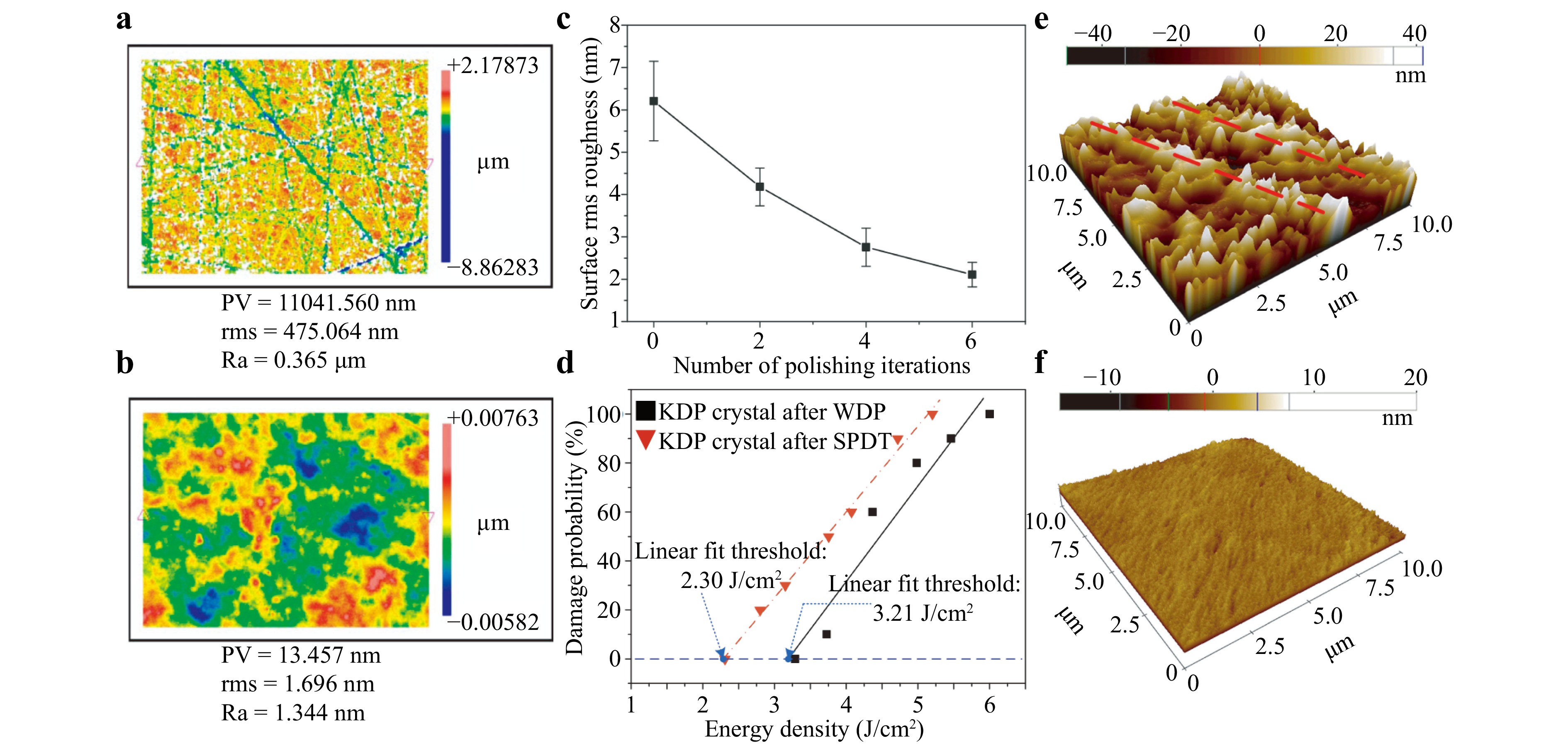
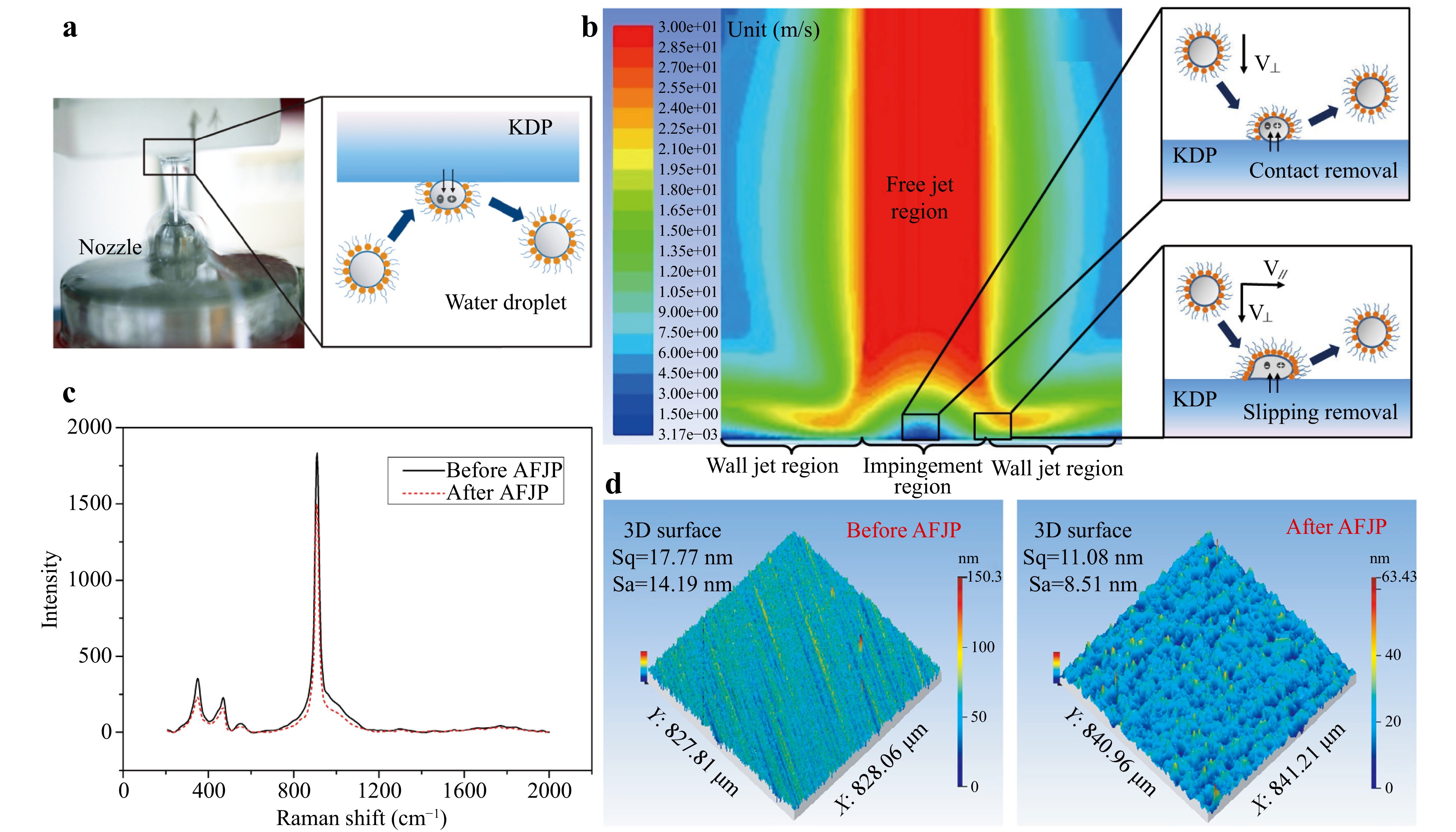
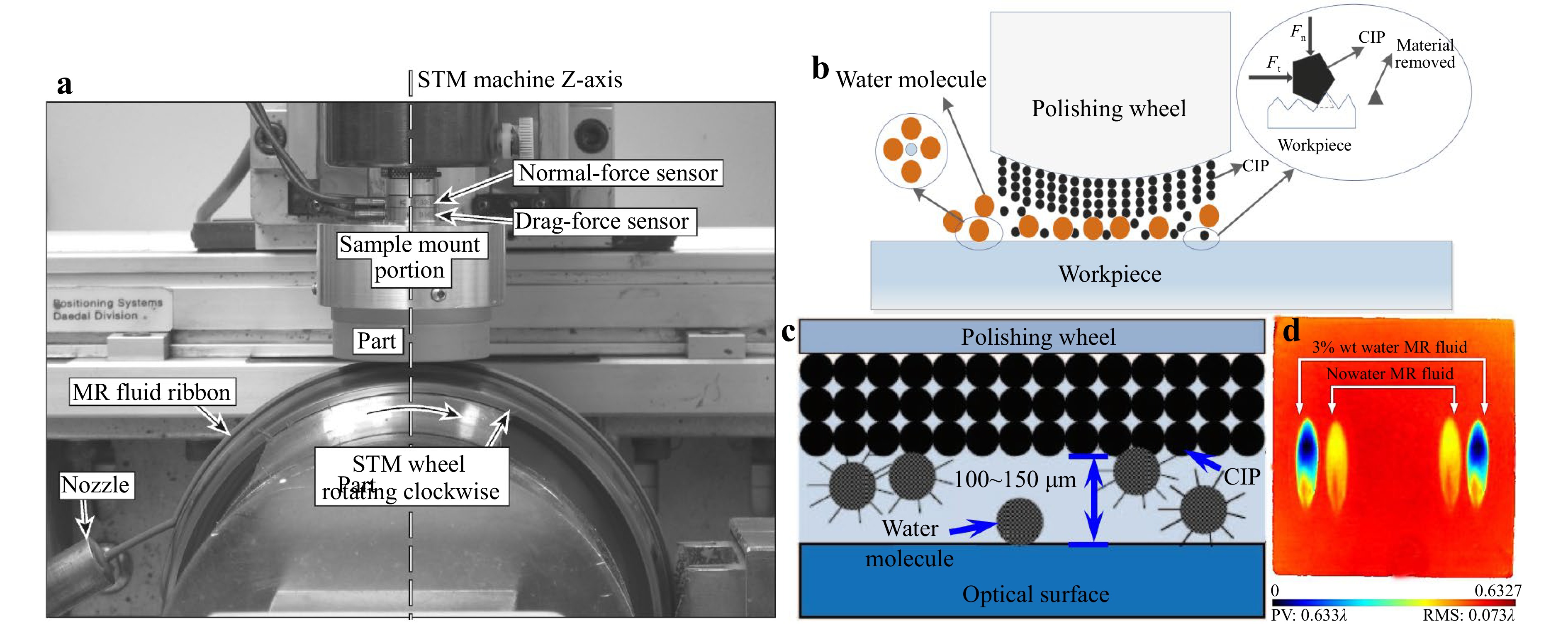
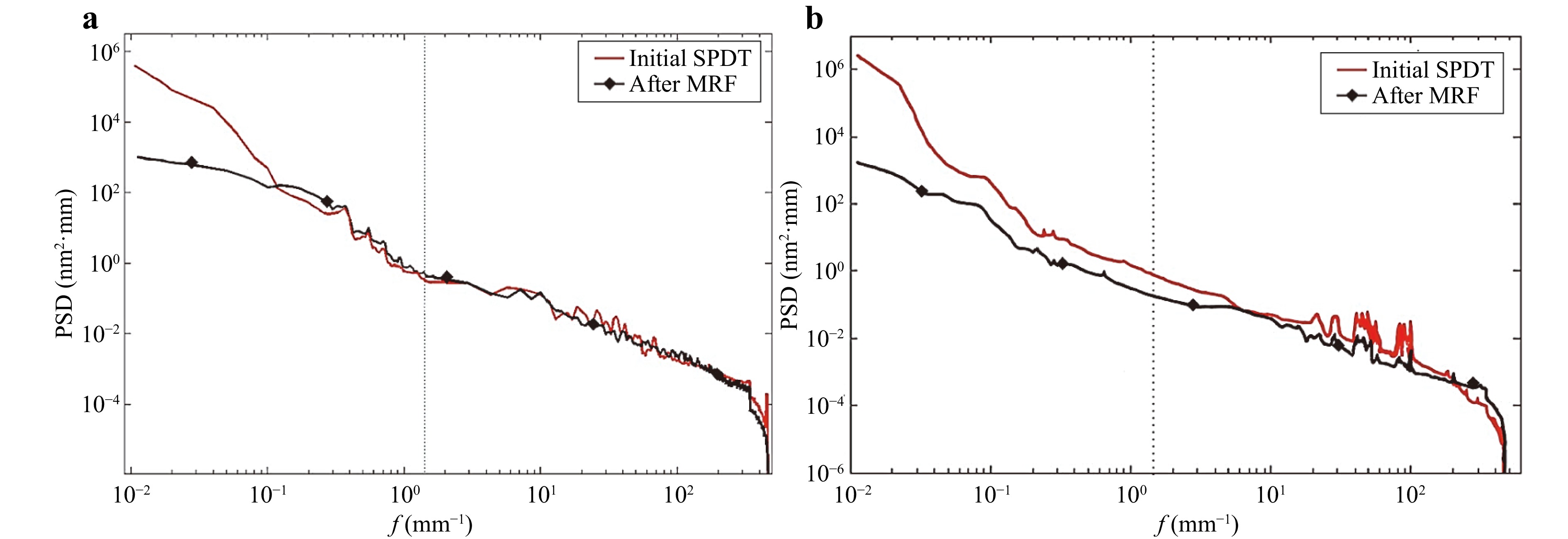
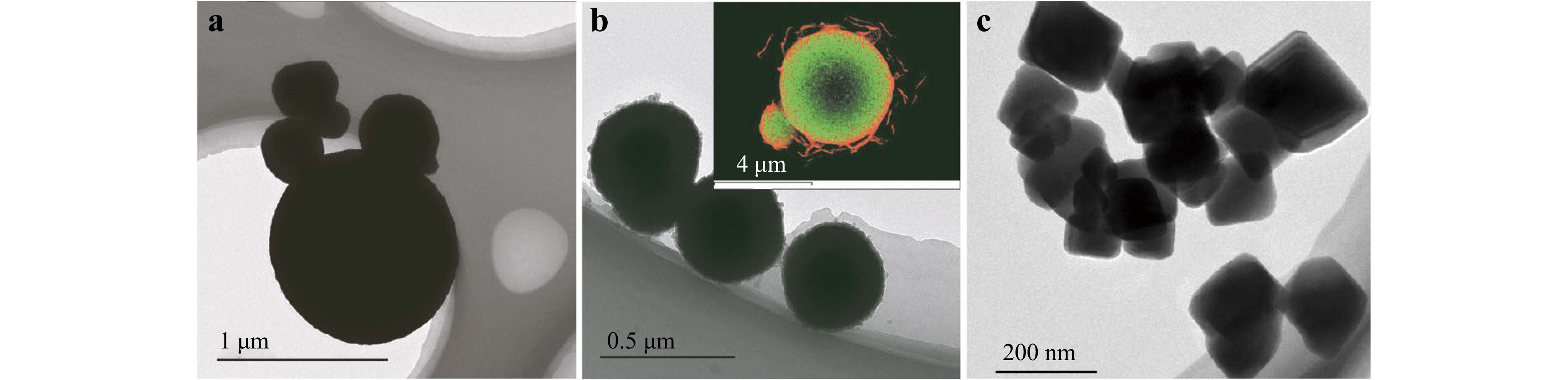
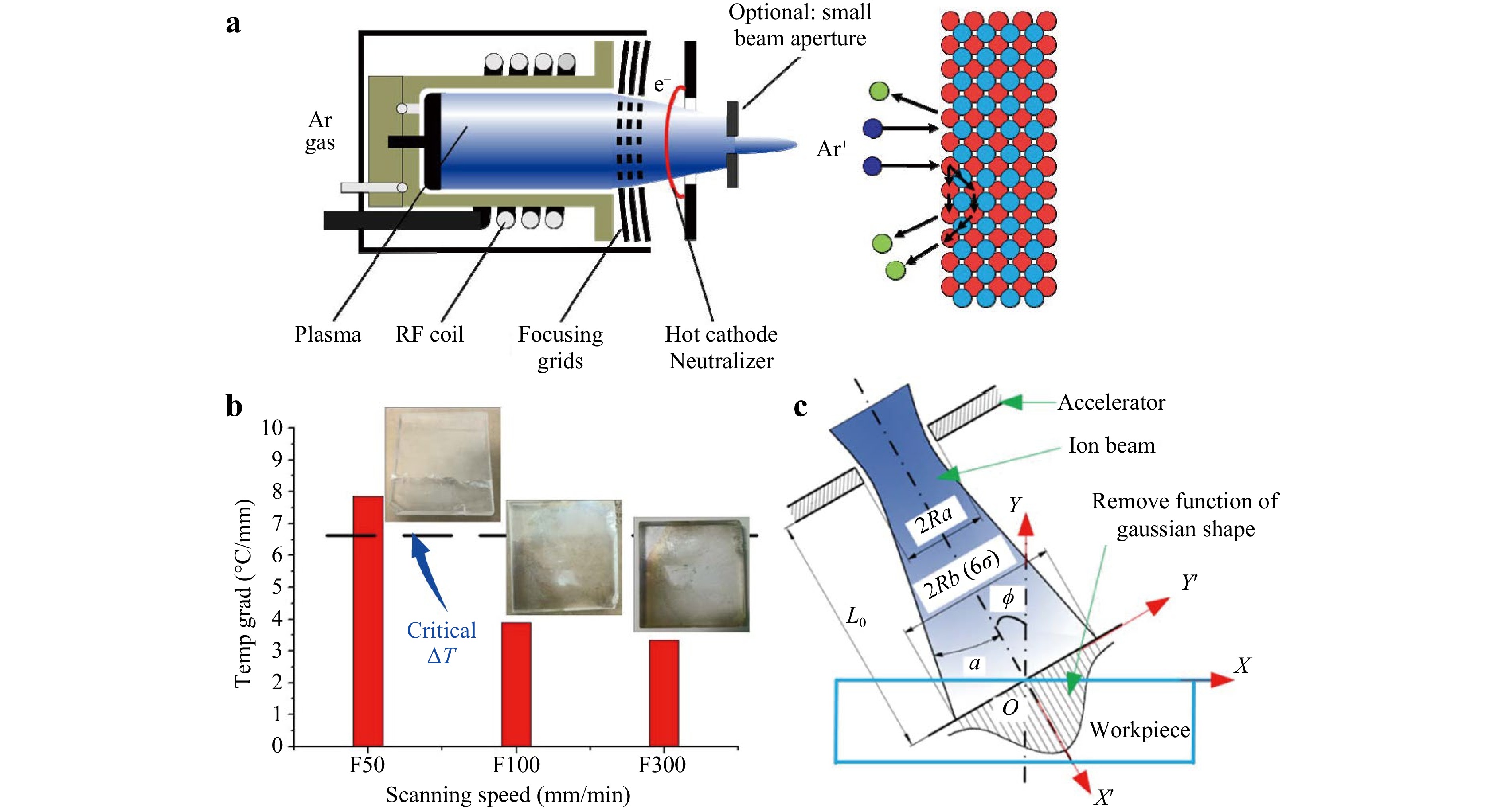
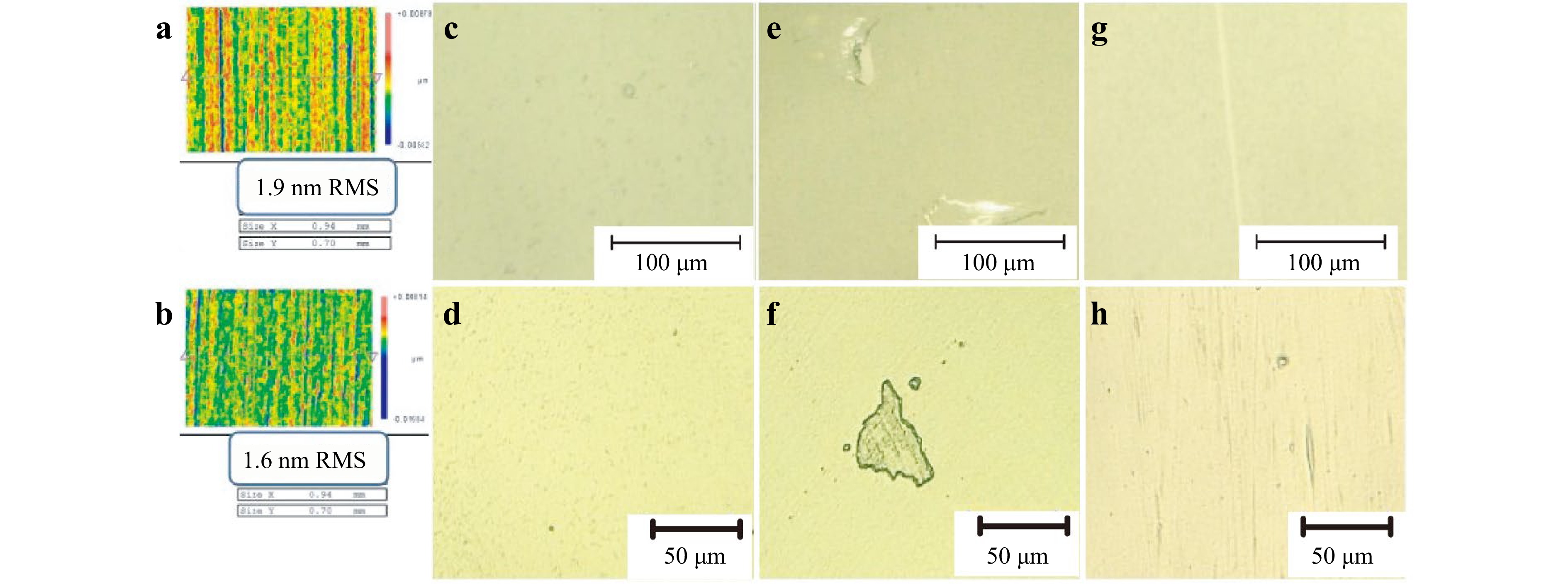
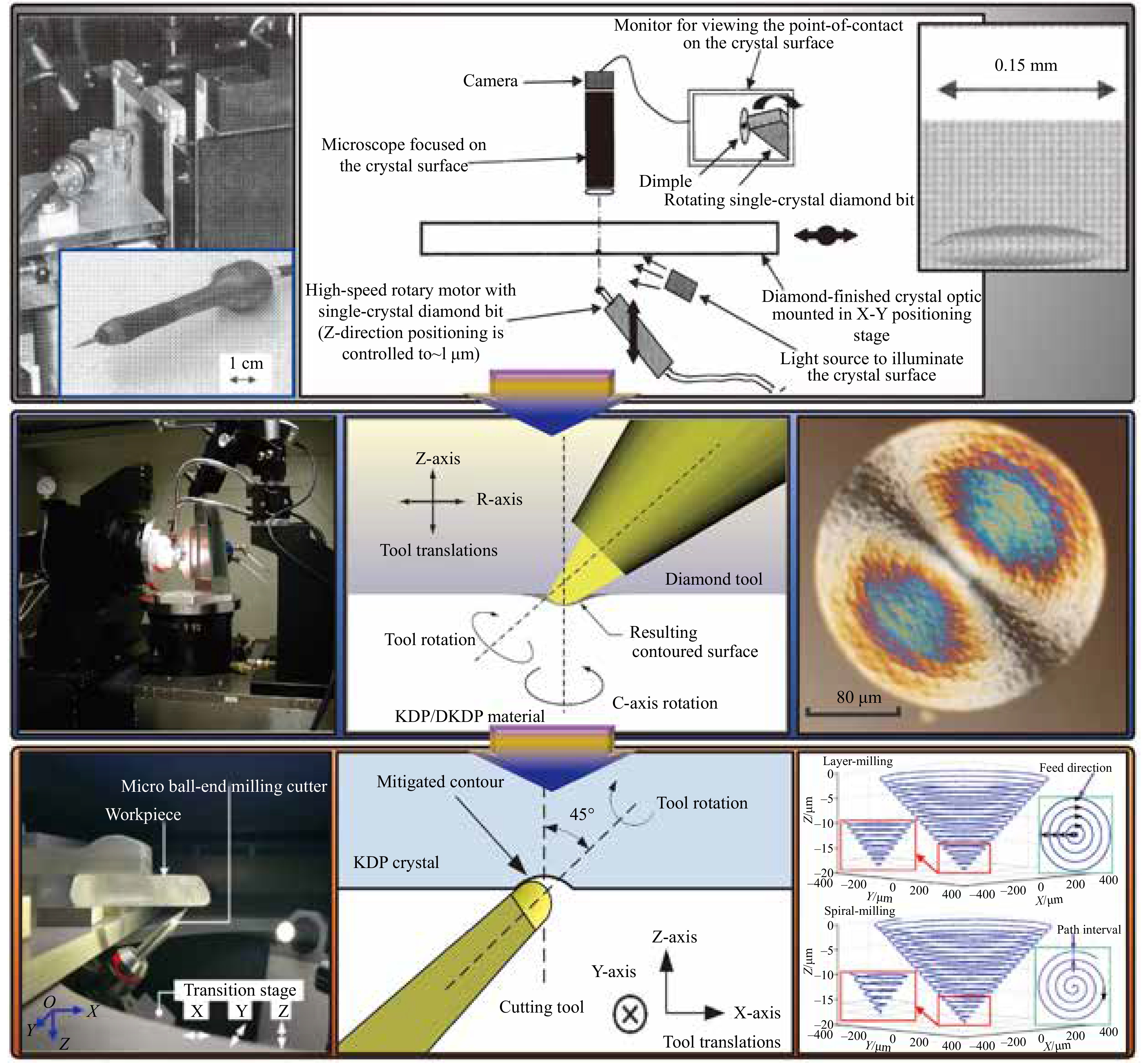
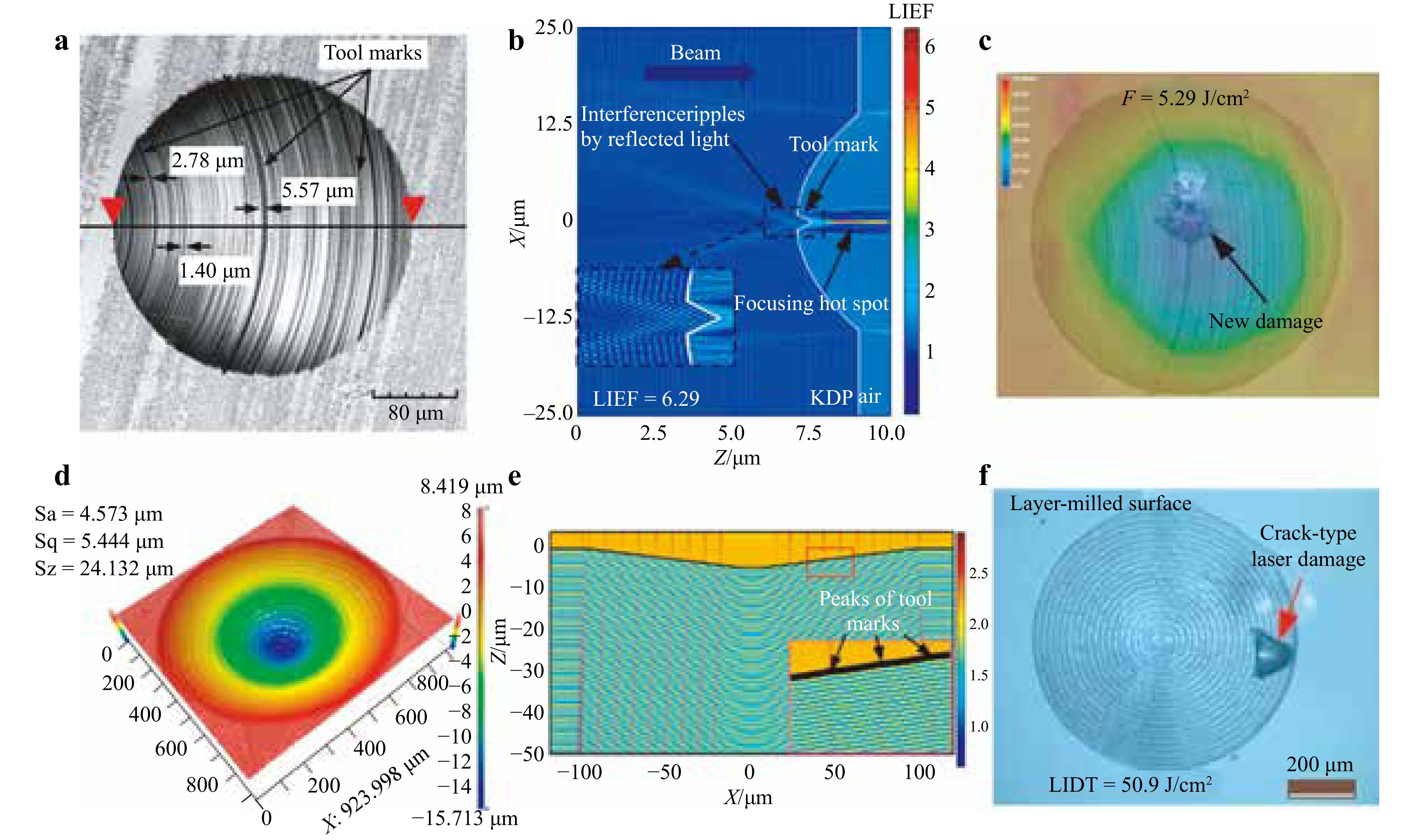
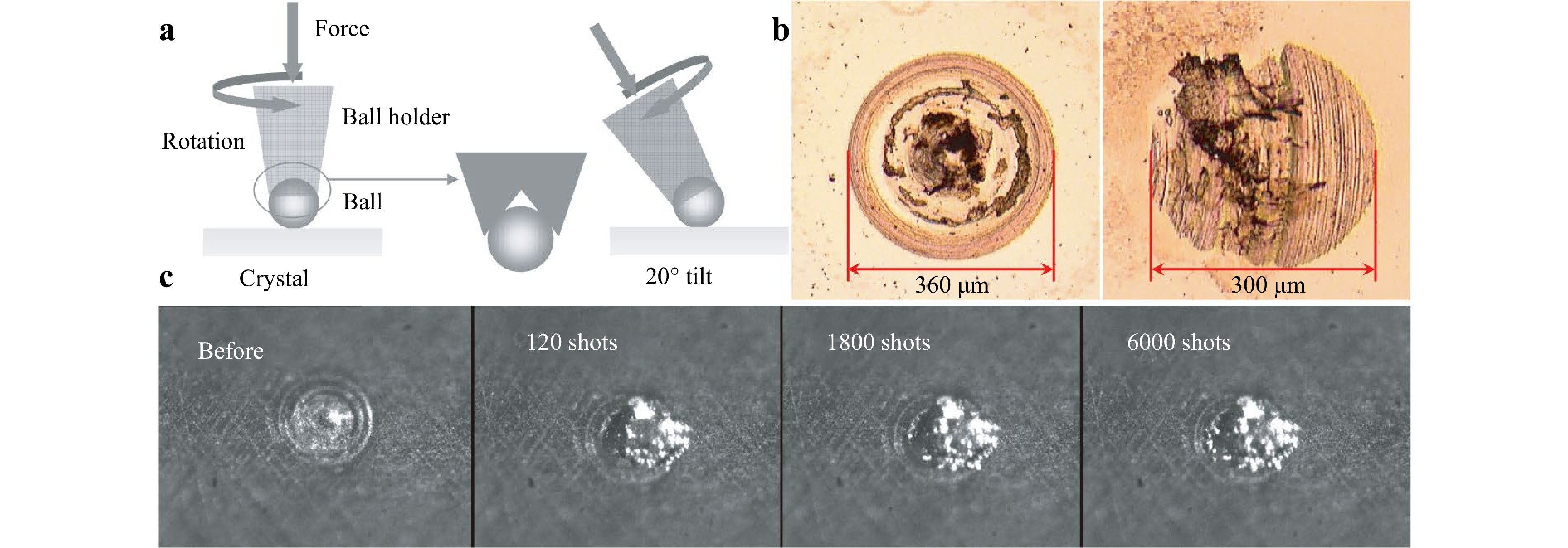
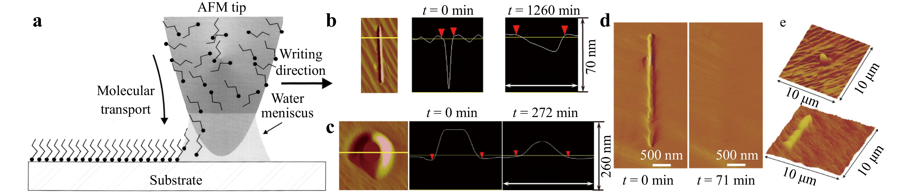
Nonlinear KHxD2-xPO4 crystal optics, e.g. second/third-harmonic generators, are components of high-energy/power laser facilities, which deliver and convert 1ω, 2ω, and 3ω lasers to obtain extreme fusion ignition conditions (high pressures, high temperatures, etc.). A laser facility requires extremely high-precision and defect-free KHxD2-xPO4 optics with meter-sized apertures to control laser beams temporally, spatially, and spectrally, yielding great ultra-precision manufacturing challenges. Meanwhile, when irradiated by intense laser pulses, laser damage precursors (e.g. manufacturing-induced micro-cracks, scratches, and debris) in the optics would spark off laser-induced surface damage and damage growth, which have been the bottleneck problems preventing the promotion of the output energies of these laser facilities. Under this circumstance, a variety of advanced optical manufacturing techniques have been developed to regulate these precursors to improve the laser damage resistance of the optics. However, the damage thresholds (8–9 J/cm2) of these optics are still far below the intrinsic threshold of the KHxD2-xPO4 (147–200 J/cm2). Furthermore, the batch engineering applications of these techniques remains challenged by the meter-sized apertures of the optics and their soft-brittle, easily deliquescent, anisotropic, and temperature-sensitive material properties, among others. This work summarises the development of state-of-the-art advanced manufacturing techniques and their problems applied in regulating laser damage precursors in the functional KHxD2-xPO4 optics. Because of their soft-brittle, deliquescent, anisotropic nature, etc., these crystal optics are difficult to cut, and new damage precursors (i.e. corrosion, debris, tool marks) could be introduced in the manufacturing processes. The challenges and their solutions are emphatically discussed and analysed in this paper. The latest development trends for the manufacture of high-performance KHxD2-xPO4 optics with high laser damage resistance are also explored. This work could provide basis and guidance for the function-oriented high-performance manufacturing of KHxD2-xPO4 optics and other functional optics with similar material properties, advancing the development of high-energy/power laser facilities.
Published. 2025, 6(3)
: 575-581
doi: 10.37188/lam.2025.047
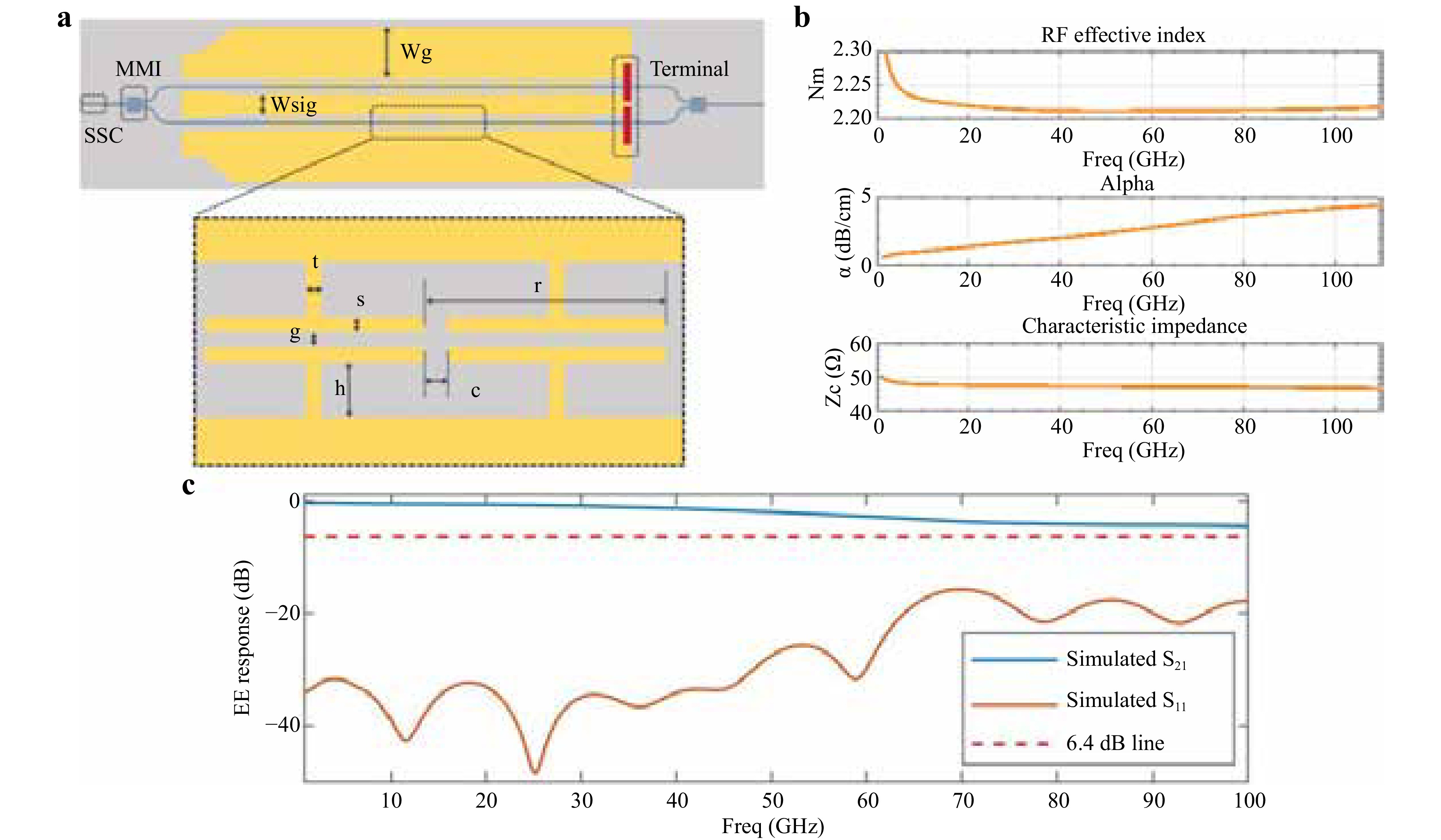
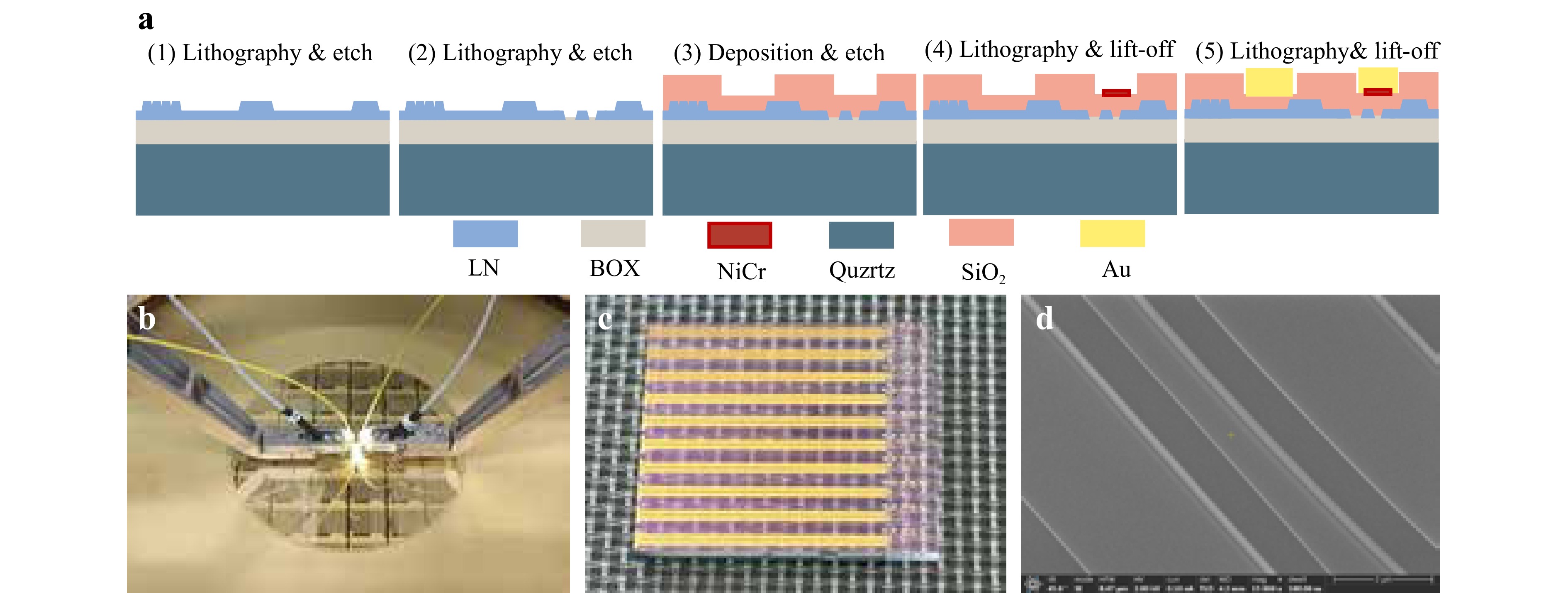
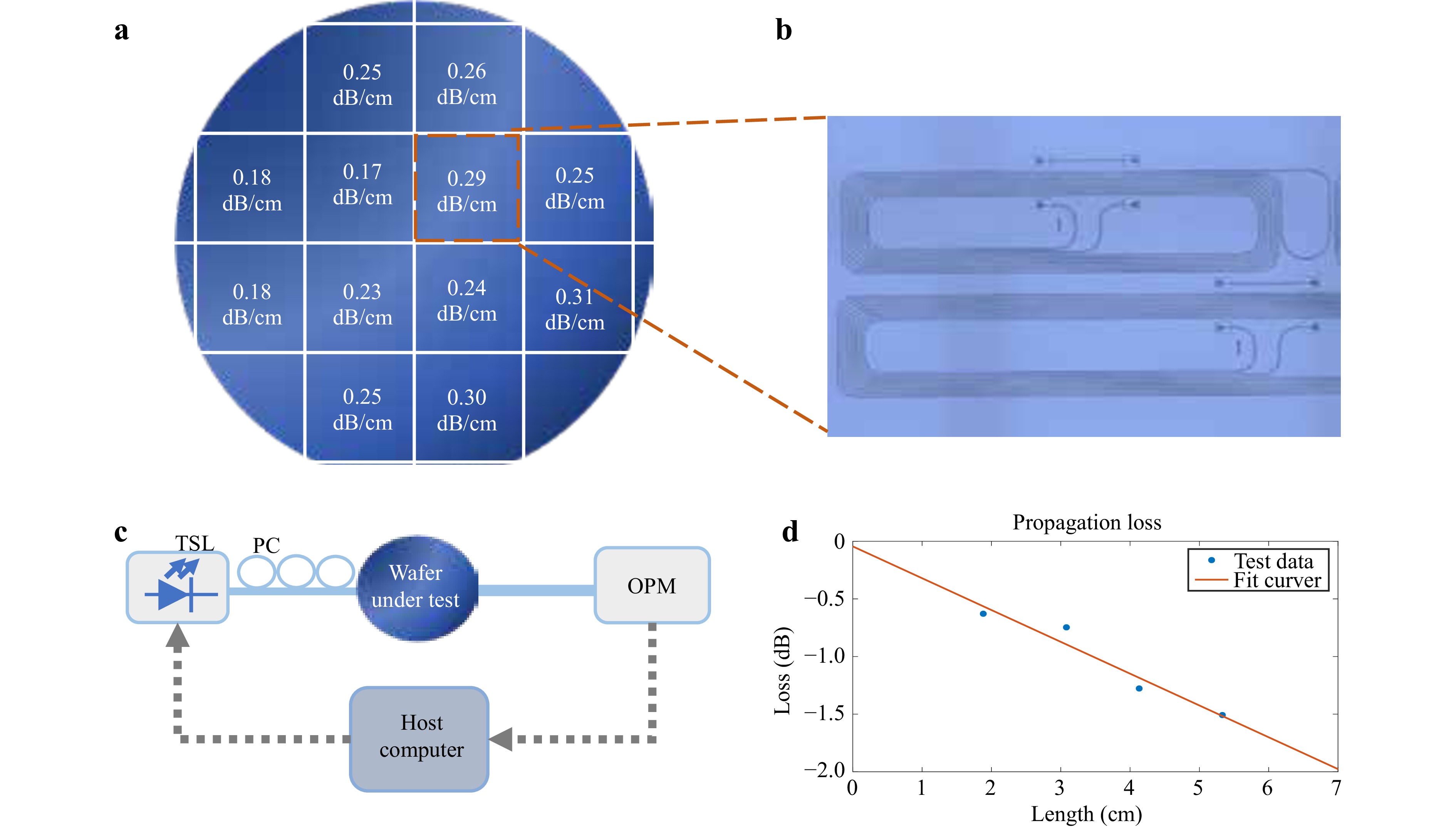
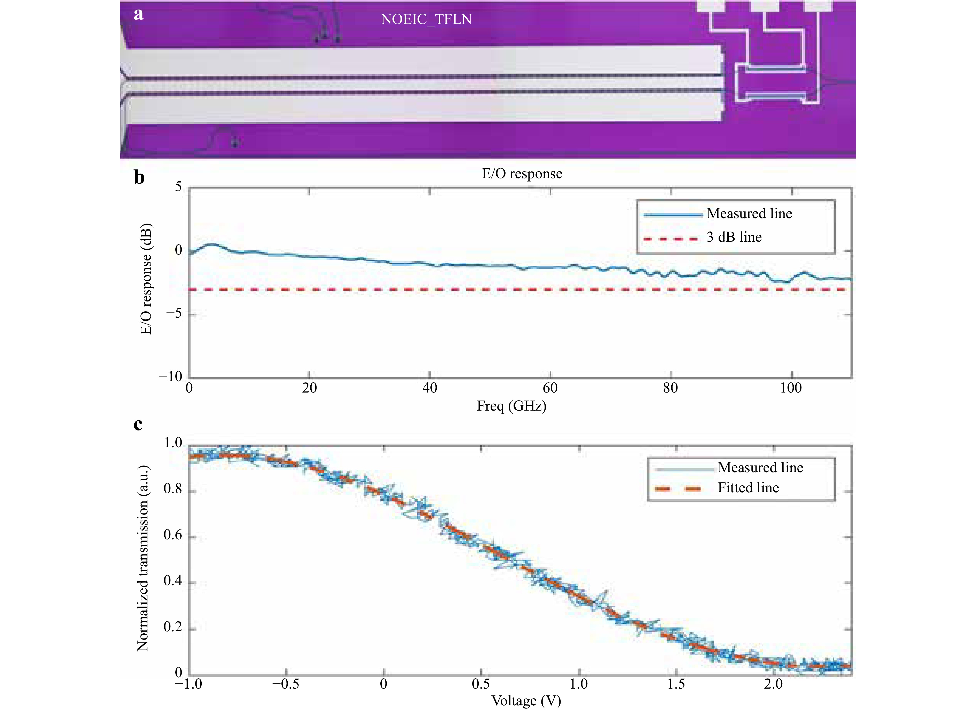
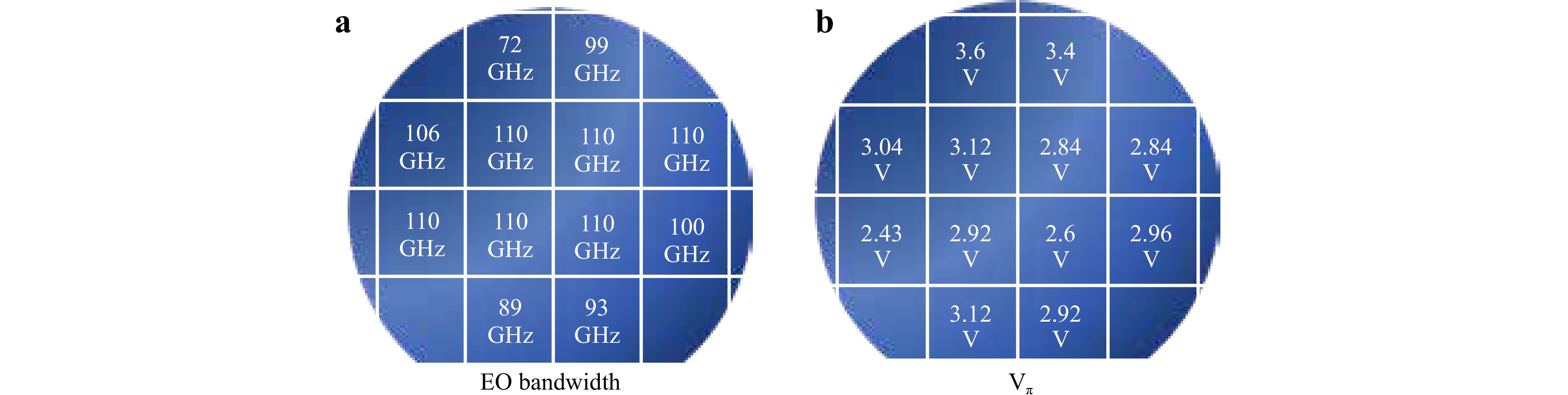
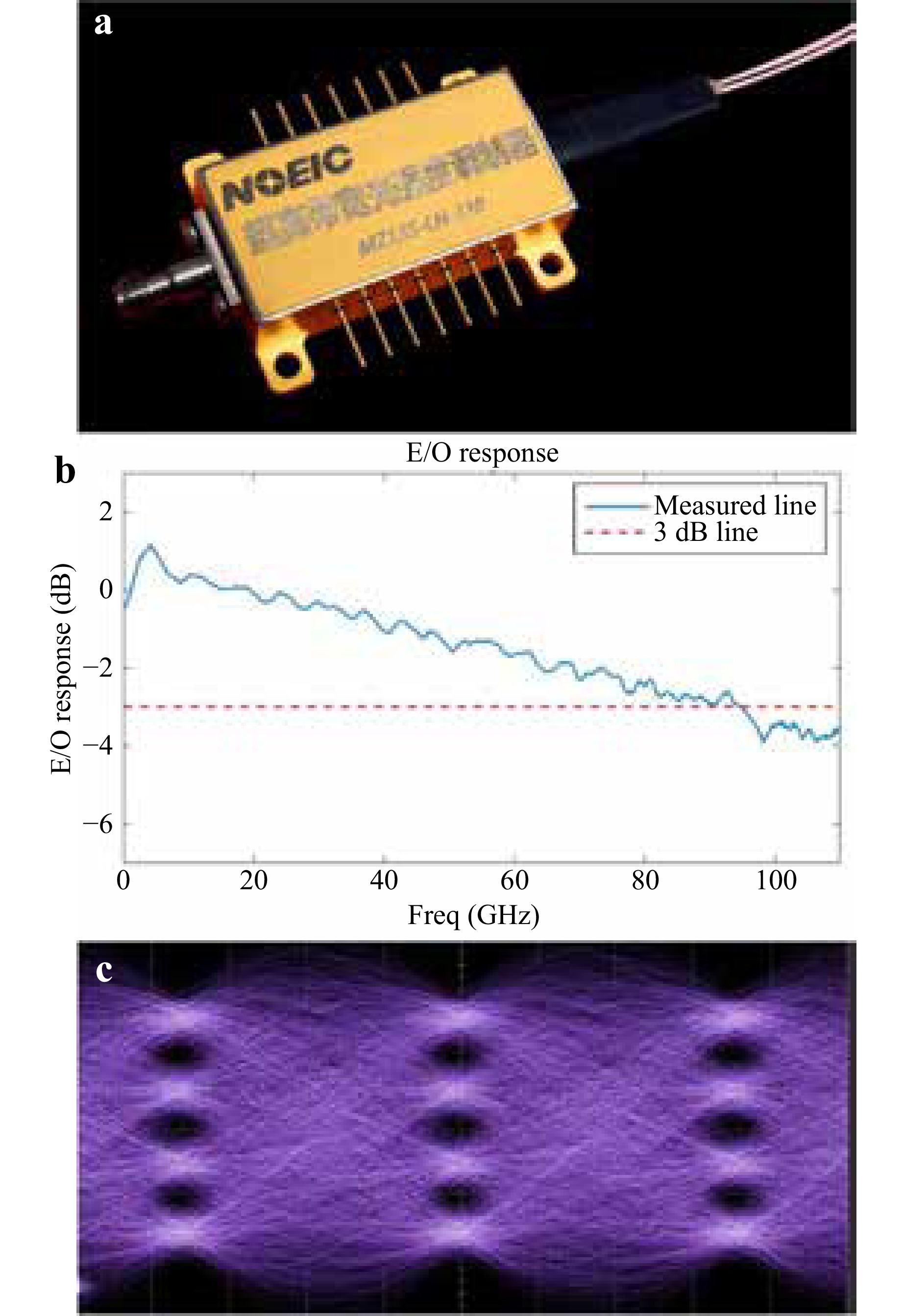
The continuous growth in data centre traffic, especially from artificial intelligence and machine learning workloads, is driving increased single carrier line rates. High-bandwidth electro-optic modulators are essential for supporting 400 Gbit/s per lane transmission. While recent advancements have demonstrated bandwidths greater than 110 GHz at the die level, this throughput is insufficient for current and future applications like data centre optical interconnects. This paper presents a photonic platform based on 4-inch thin-film lithium niobate wafers with a quartz substrate, offering high yield, low loss and high bandwidth. This platform achieves waveguide propagation loss of < 0.4 dB/cm. The thin-film lithium niobate modulators fabricated on this platform can attain a bandwidth exceeding 110 GHz and possess a half-wave voltage (Vπ) lower than 3 V, with the modulator yield reaching 50%. Additionally, by employing deep-ultraviolet lithography and a metal lift-off process, the platform can be extended to larger wafer sizes (e.g., 6 or 8 inches). This significant increase in wafer-level throughput for 110 GHz electro-optic modulators can greatly enhance data centre optical interconnect capabilities.

 Email
Email RSS
RSS